

Page 1
User's Guide
SLAU261 – November 2008
TLV320AIC3107EVM-K
This user's guide describes the characteristics, operation, and use of the TLV320AIC3107EVM-K. This
evaluation module (EVM) allows the user to evaluate the TLV320AIC3107 audio codec. The
TLV320AIC3107 is a complete 2-channel audio codec with an integrated Class-D speaker amplifier. It also
has many inputs and outputs, extensive audio routing, mixing, and effects capabilities. A complete circuit
description, schematic diagram, and bill of materials are included. Note that the TLV320AIC3107 only
uses the I2C™ bus for register control. Any references to the SPI control bus in this document is due to
the presence of this interface on the USB-MODEVM motherboard.
Note: For a quick start, go directly to Section 3.1 Software Installation, followed by Section 3.2
EVM Connections, and then to Section 4.1 Quick Start Tabs.
The following related documents are available through the Texas Instruments Web site at www.ti.com .
EVM-Compatible Device Data Sheets
Device Literature Number
TLV320AIC3107 SLOS545
TAS1020B SLES025
REG1117-3.3 SBVS001
TPS767D318 SLVS209
SN74LVC125A SCAS290
SN74LVC1G125 SCES223
SN74LVC1G07 SCES296
Contents
1 EVM Overview ............................................................................................................... 3
2 EVM Description and Basics ............................................................................................... 3
3 TLV320AIC3107EVM-K Setup and Installation .......................................................................... 7
4 TLV320AIC3107EVM Software ............................................................................................ 8
Appendix A EVM Connector Descriptions ................................................................................... 33
Appendix B TLV320AIC3107EVM Schematic ............................................................................... 36
Appendix C TLV320AIC3107EVM Layout Views ........................................................................... 38
Appendix D TLV320AIC3107EVM Bill of Materials ......................................................................... 41
Appendix E USB-MODEVM Schematic ...................................................................................... 43
Appendix F USB-MODEVM Bill of Materials ................................................................................ 44
Appendix G USB-MODEVM Protocol ......................................................................................... 46
List of Figures
1 TLV320AIC3107EVM-K Block Diagram .................................................................................. 4
2 Quick Start - USB-MODEM Configurations .............................................................................. 8
3 Quick Start - Preset Configurations Tab .................................................................................. 9
4 Main Software Screen .................................................................................................... 10
5 ................................................................................................................................ 11
6 Audio Input/ADC Tab ..................................................................................................... 12
I2C, I2S are trademarks of Koninklijke Philips Electronics N.V..
Windows is a trademark of Microsoft Corporation.
LabView is a trademark of National Instruments.
SLAU261 – November 2008 TLV320AIC3107EVM-K 1
Submit Documentation Feedback
Page 2

www.ti.com
7 Bypass Paths Tab .......................................................................................................... 13
8 Audio Interface Tab ....................................................................................................... 14
9 Clocks Tab ................................................................................................................. 15
10 GPIO1 Tab ................................................................................................................. 17
11 AGC Tab .................................................................................................................... 18
12 Left AGC Settings .......................................................................................................... 19
13 Advanced .................................................................................................................... 19
14 Filters Tab .................................................................................................................. 20
15 ADC High-Pass Filters .................................................................................................... 21
16 ADC High-Pass Filter Settings ........................................................................................... 21
17 DAC Filters .................................................................................................................. 22
18 De-emphasis Filters ........................................................................................................ 22
19 Enabling Filters ............................................................................................................ 23
20 Shelf Filters ................................................................................................................. 23
21 EQ Filters ................................................................................................................... 24
22 Analog Simulation Filters ................................................................................................. 24
23 Preset Filters ............................................................................................................... 25
24 User Filters ................................................................................................................. 25
25 3D Effect Settings ......................................................................................................... 26
26 DAC/Line Outputs Tab .................................................................................................... 26
27 Output Stage Configuration Tab ......................................................................................... 28
28 High Power Outputs Tab ................................................................................................. 29
29 Class-D Output Tab ........................................................................................................ 30
30 Command Line Interface Tab ............................................................................................ 31
31 File Menu ................................................................................................................... 32
C-1 Assembly layer ............................................................................................................. 38
C-2 Top Layer .................................................................................................................... 38
C-3 Layer 3 ....................................................................................................................... 39
C-4 Layer 4 ....................................................................................................................... 39
C-5 Bottom Layer ................................................................................................................ 40
List of Tables
1 USB-MODEVM SW2 Settings ............................................................................................. 5
2 List of Stand-alone Jumpers ............................................................................................... 5
3 Switch SW1 Configurations ................................................................................................ 6
4 Switch SW2 Configurations ................................................................................................ 6
5 Switch SW3 Configurations ................................................................................................ 6
A-1 Analog Input/Output Connectors ......................................................................................... 33
A-2 Block A and Block B Digital Interface Pinout ........................................................................... 34
A-3 Power Supply Pinout ....................................................................................................... 35
D-1 TLV320AIC3107EVM Bill of Materials ................................................................................... 41
F-1 USB-MODEVM Bill of Materials .......................................................................................... 44
G-1 USB Control Endpoint HIDSETREPORT Request .................................................................... 46
G-2 Data Packet Configuration ................................................................................................ 46
G-3 GPIO Pin Assignments .................................................................................................... 49
2 TLV320AIC3107EVM-K SLAU261 – November 2008
Submit Documentation Feedback
Page 3

www.ti.com
1 EVM Overview
1.1 Features
1.2 Introduction
EVM Overview
• Full-featured evaluation board for the TLV320AIC3107 2-channel audio codec with integrated Class-D
amplifier.
• Modular design for use with a variety of digital signal processor (DSP) and microcontroller interface
boards.
• USB connection to PC provides power, control, and streaming audio data for easy evaluation.
• Onboard microphone for ADC evaluation
• Connection points for external control and digital audio signals for quick connection to other
circuits/input devices.
The TLV320AIC3107EVM-K is a complete evaluation kit, which includes a universal serial bus
(USB)-based motherboard and evaluation software for use with a personal computer (PC) running the
Microsoft Windows™ operating system (Win2000 or XP).
The TLV320AIC3107EVM is in the Texas Instruments modular EVM form factor, which allows direct
evaluation of the device performance and operating characteristics, and eases software development and
system prototyping. This EVM is compatible with the 5-6K Interface Evaluation Module (SLAU104 ) and the
HPA-MCUINTERFACE (SLAU106 ) from Texas Instruments and additional third-party boards which
supports the TI Modular EVM format.
The TLV320AIC3107EVM-K is a complete evaluation/demonstration kit, which includes a USB-based
motherboard called the USB-MODEVM Interface board and evaluation software for use with a PC running
the Microsoft Windows operating systems.
The USB connection from the PC provides power, control, and streaming audio data to the EVM for
reduced setup and configuration. The EVM also allows external control signals, audio data, and power for
advanced operation, which allows prototyping and connection to the rest of the evaluation/development
system.
2 EVM Description and Basics
This section provides information on the analog input and output, digital control, power, and general
connection of the TLV320AIC3107EVM.
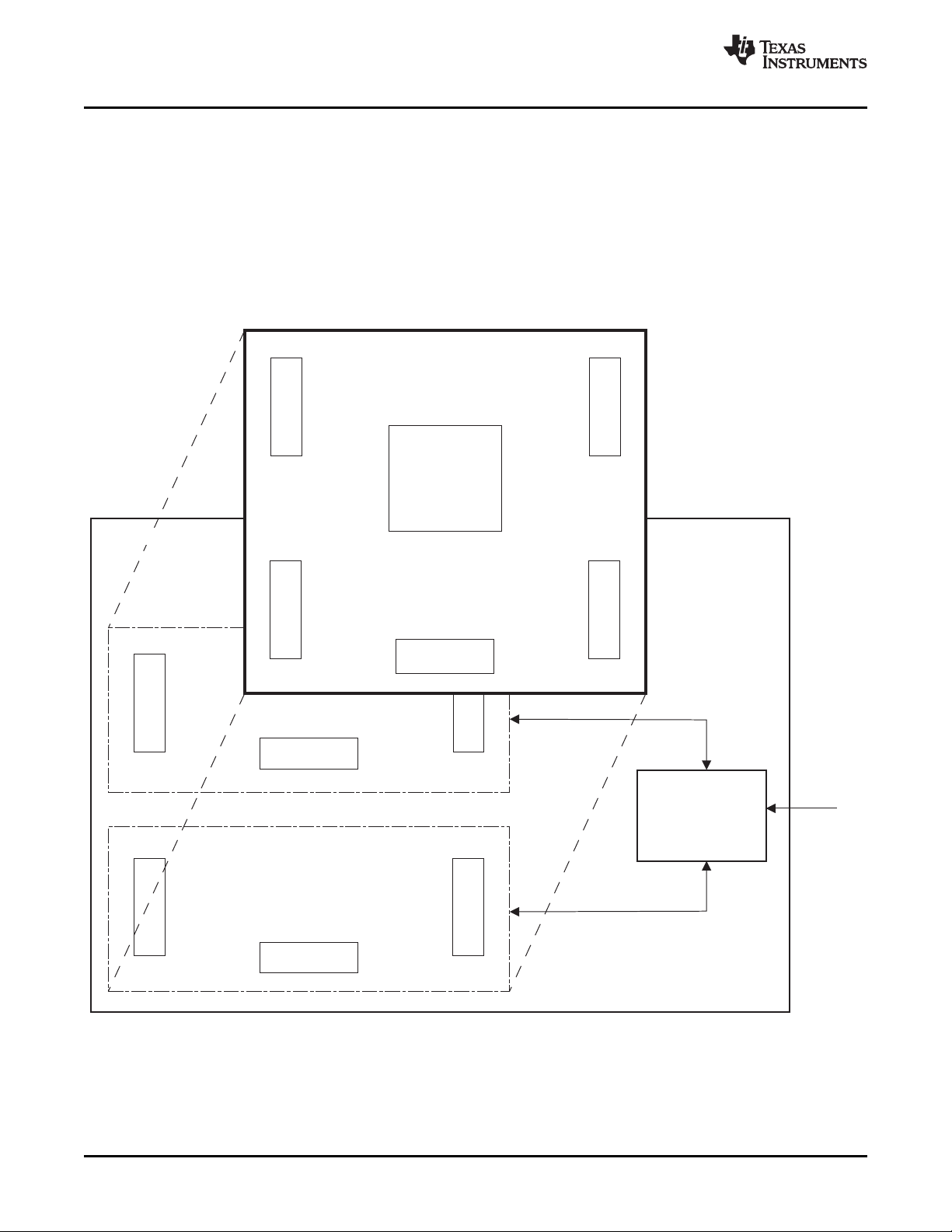
2.1 TLV320AIC3107EVM-K Block Diagram
The TLV320AIC3107EVM-K consists of two separate circuit boards, the USB-MODEVM and the
TLV320AIC3107EVM. The USB-MODEVM is built around a TAS1020B streaming audio USB controller
with an 8051-based core.
The simple diagram of Figure 1 shows how the TLV320AIC3107EVM is connected to the USB-MODEVM.
The USB-MODEVM Interface board is intended to be used in USB mode, whereas control of the installed
EVM is accomplished using the onboard USB controller device. Provision is made, however, for driving all
the data buses (I2C, I2S, etc.) externally. The source of these signals is controlled by SW2 on the
USB-MODEVM. See Table 1 for details on the switch settings.
SLAU261 – November 2008 TLV320AIC3107EVM-K 3
Submit Documentation Feedback
Page 4
EVMPosition2
EVMPosition1
TLV320AIC3107EVM
ControlInterface
TLV320AIC3107
TAS1020B
USB8051
Microcontroller
USB
I C
2
I S
2
AudioInterface
USB-MODEVM
EVM Description and Basics
2.1.1 USB-MODEVM Interface Board
The simple diagram of Figure 1 shows only the basic features of the USB-MODEVM Interface board.
When connecting the TLV320AIC3107EVM to the USB-MODEVM, use care to avoid bending the
connecting pins. The two boards can only be connected in one way. It is suggested to first align with the
10-pin connectors (J3 on the TLV320AIC3107EVM and J18A on the USB-MODEVM) and then gently
push all the connectors together until the boards are seated.
In the factory configuration, the board is ready to use with the TLV320AIC3107EVM. To view all the
functions and configuration options available on the USB-MODEVM board, see the USB-MODEVM
Interface Board schematic in Appendix E.
www.ti.com
Figure 1. TLV320AIC3107EVM-K Block Diagram
TLV320AIC3107EVM-K 4 SLAU261 – November 2008
Submit Documentation Feedback
Page 5

www.ti.com
2.2 Default Configuration and Connections
2.2.1 USB-MODEVM
Table 1 provides a list of the SW2 settings on the USB-MODEVM. For use with the TLV320AIC3107EVM,
SW-2 positions 1 through 7 must be set to ON (LO), whereas SW-2.8 must be set to OFF (HI).
SW-2 Switch Number Label Switch Description
1 A0 USB-MODEVM EEPROM I2C Address A0
2 A1 USB-MODEVM EEPROM I2C Address A1
3 A2 USB-MODEVM EEPROM I2C Address A2
4 USB I2S™ I2S Bus Source Selection
5 USB MCK I2S Bus MCLK Source Selection
6 USB SPI SPI Bus Source Selection
7 USB RST RST Source Selection
8 EXT MCK External MCLK Selection
EVM Description and Basics
Table 1. USB-MODEVM SW2 Settings
ON: A0 = 0
OFF: A0 = 1
ON: A1 = 0
OFF: A1 = 1
ON: A2 = 0
OFF: A2 = 1
ON: I2S Bus connects to TAS1020
OFF: I2S Bus connects to USB-MODEVM J14
ON: MCLK connects to TAS1020
OFF: MCLK connects to USB-MODEVM J14
ON: SPI Bus connects to TAS1020
OFF: SPI Bus connects to USB-MODEVM J15
ON: EVM Reset Signal comes from TAS1020
OFF: EVM Reset Signal comes from USB-MODEVM J15
ON: MCLK Signal is provided from USB-MODEVM J10
OFF: MCLK Signal comes from either selection of SW2-5
2.2.2 TLV320AIC3107EVM Jumpers and Switches
Table 2 provides a list of jumpers found on the EVM and their factory default conditions.
Table 2. List of Stand-alone Jumpers
Jumper Jumper Default
Number Type Position Jumper Description
W1 2-pin soldered AVDD_ADC power
W2 2-pin soldered DRVDD power (DRVDD1 on EVM).
W3 2-pin soldered DRVDD power (DRVDD2 on EVM).
W3 2-pin soldered AVDD_DAC power.
W5 2-pin soldered SPVDD power.
W7 2-pin soldered DVDD power.
W8 2-pin soldered IOVDD power.
W9 3-pin 2-3 Mic bias select. Connect 1-2 to use AIC3107 Mic Bias. Connect 2-3 to use EVM 3.3V Mic Bias.
W10 2-pin Open Connect EVM Onboard Mic to AIC3107 MIC3R input.
W11 2-pin Open Connect EVM Onboard Mic to AIC3107 MIC3L input.
W12 2-pin Open Enable 16-ohm load for HPL output test.
W13 2-pin Open Enable 16-ohm load for HPR output test.
W14 3-pin 1-2 IOVDD select. Connect 1-2 for IOVDD=+1.8V. Connect 2-3 for IOVDD=+3.3V.
W15 2-pin Open GPIO1 access point.
W16 2-pin Installed Software reset enable.
SLAU261 – November 2008 TLV320AIC3107EVM-K 5
Submit Documentation Feedback
Page 6
EVM Description and Basics
Table 2. List of Stand-alone Jumpers (continued)
Jumper Jumper Default
Number Type Position Jumper Description
W17 2-pin Open Selects onboard EEPROM as TAS1020B Firmware Source.(Not Used). Note that for this EVM the Firmware Source
W18 2-pin Open Selects SWOUTP to J-18. Caution: Make sure that the Class-D Output is Disabled before Installing W18.
W19 2-pin Open Selects SWOUTM to J-18. Caution: Make sure that the Class-D Output is Disabled before Installing W19.
EEPROM is on the USB-MODEVM.
Table 3. Switch SW1 Configurations
EVM Connector Terminal Number SW1 Switch Position = DIFF (Differential Inputs) SW1 Switch Position = SE = Single-Ended
Connector (Terminal 2 is always Ground.) Inputs
J6 Terminal 1 Input to AIC3107-pin 4 = LINE1LP Input to AIC3107-pin 4 = LINE1LP
Terminal 3 Input to AIC3107-pin 3 = MICDET/ LINE1LM Input to AIC3107-pin 5 = LINE1RP
J7 Terminal 1 Input to AIC3107-pin 5 = LINE1RP Input to AIC3107-pin 9 = MIC3R/LINE2RM
Terminal 3 Input to AIC3107-pin 6 = MIC3L/ LINE1RM Input to AIC3107-pin 6 = MIC3L/LINE1RM
J8 Terminal 1 Input to AIC3107-pin 7 = LINE2LP Input to AIC3107-pin 7 = LINE2LP
Terminal 3 Input to AIC3107-pin 8 = LINE2RP/ LINE2LM Input to AIC3107-pin 8 = LINE2RP/LINE2LM
Table 4. Switch SW2 Configurations
SW2 Switch Position = CAP SW2 Switch Position = Capacitor-less
47- µ F capacitors in-line with HPLOUT and HPROUT to J10 (Referenced to HPLOUT and HPROUT Direct Coupled to J10 (Referenced to HPCOM)
Ground)
www.ti.com
Table 5. Switch SW3 Configurations
SW3 Switch Position = EXT. SW3 Switch Position = +5VA
User Provides an External Power Supply for SVDD (Class-D Power Amplifier EVM 5-VDC Supply used for SVDD (Class-D Power Amplifier Supply)
Supply), Max Value = 5 VDC
2.3 Power Connections
The TLV320AIC3107 can be powered independently when being used in stand-alone operation or by the
USB-MODEVM when it is plugged onto the motherboard.
2.3.1 Stand-Alone Operation
When used as a stand-alone, power is applied to J15 directly; be sure to reference the supplies to the
appropriate grounds on that connector.
CAUTION
Before applying power to the EVM, you must verify that all power supplies are
within the safe operating limits as indicated in the TLV320AIC3107 data sheet .
J15 provides connection to the common power bus for the TLV320AIC3107EVM. Power is supplied on the
pins listed in Table A-3 .
The TLV320AIC3107EVM-K motherboard (the USB-MODEVM Interface board) supplies power to J15 of
the TLV320AIC3107EVM. Power for the motherboard is supplied either through its USB connection or via
terminal blocks on that board.
2.3.2 USB-MODEVM Operation
The USB-MODEVM Interface board can be powered from several different sources:
• USB
• 6-Vdc to 10-Vdc ac/dc external wall supply (not included)
6 TLV320AIC3107EVM-K SLAU261 – November 2008
Submit Documentation Feedback
Page 7

www.ti.com
• Laboratory power supply
When powered from the USB connection, JMP6 must have a shunt from pins 1–2 (this is the default
factory configuration). When powered from 6 Vdc-10 Vdc, either through the J8 terminal block or J9 barrel
jack, JMP6 must have a shunt installed on pins 2–3. If power is applied in any of these ways, onboard
regulators generate the required supply voltages, and no further power supplies are necessary.
If laboratory supplies are used to provide the individual voltages required by the USB-MODEVM Interface,
JMP6 must have no shunt installed. Voltages are then applied to J2 (+5VA), J3 (+5VD), J4 (+1.8VD), and
J5 (+3.3VD). The +1.8VD and +3.3VD can also be generated on the board by the onboard regulators from
the +5VD supply; to enable this configuration, the switches on SW1 need to be set to enable the
regulators by placing them in the ON position (lower position, looking at the board with text reading
right-side up). If +1.8VD and +3.3VD are supplied externally, disable the onboard regulators by placing
SW1 switches in the OFF position.
Each power supply voltage has an LED (D1-D7) that lights when the power supplies are active.
3 TLV320AIC3107EVM-K Setup and Installation
The following section provides information on using the TLV320AIC3107EVM-K, including set up, program
installation, and program usage.
Note: If using the EVM in stand-alone mode, the software must be installed per the following
instructions, but the hardware configuration may be different.
TLV320AIC3107EVM-K Setup and Installation
3.1 Software Installation
3.2 EVM Connections
1. Locate the installation file on the CD-ROM included with the EVM or download the latest version of the
software located on the AIC3107 Product Page .
2. Unzip the installation file by clicking on the self-extracting zip file.
3. Install the EVM software by double-clicking the Setup executable and follow the directions. Users may
be prompted to restart their computers.
This installs all the TLV320AIC3107 software and required drivers onto the PC.
1. Ensure that the TLV320AIC3107EVM is installed on the USB-MODEVM Interface board, aligning J1,
J2, J3, J4, and J5 with the corresponding connectors on the USB-MODEVM.
2. Verify that the jumpers and switches are in their default conditions.
3. Attach a USB cable from the PC to the USB-MODEVM Interface board. The default configuration
provides power, control signals, and streaming audio via the USB interface from the PC. On the
USB-MODEVM, LEDs D3-6 light to indicate the power is being supplied from the USB.
4. For the first connection, the PC recognizes new hardware and begins an initialization process. The
user may be prompted to identify the location of the drivers or allow the PC to automatically search for
them. Allow the automatic detection option.
5. Once the PC confirms that the hardware is operational, D2 on the USB-MODEVM lights to indicate that
the firmware has been loaded and the EVM is ready for use. If the LED is not lighted, verify that the
drivers were installed, try to unplug, and restart at Step 3.
After the TLV320AIC3107EVM-K software installation (described in Section 3.2 ) is complete, evaluation
and development using the target TLV320AIC3107 can begin.
The TLV320AIC3107EVM software now can be launched. The user sees an initial screen that looks
similar to Figure 4 .
SLAU261 – November 2008 TLV320AIC3107EVM-K 7
Submit Documentation Feedback
Page 8
TLV320AIC3107EVM Software
4 TLV320AIC3107EVM Software
The following section discusses the details and operation of the EVM software.
Note: For configuration of the codec, the TLV320AIC3107 block diagram located in the
TLV320AIC3107 data sheet is a good reference to help determine the signal routing. A
pop-up detailed block diagram also is provided in the TLV320AIC3107 GUI software.
4.1 Quick Start Tabs
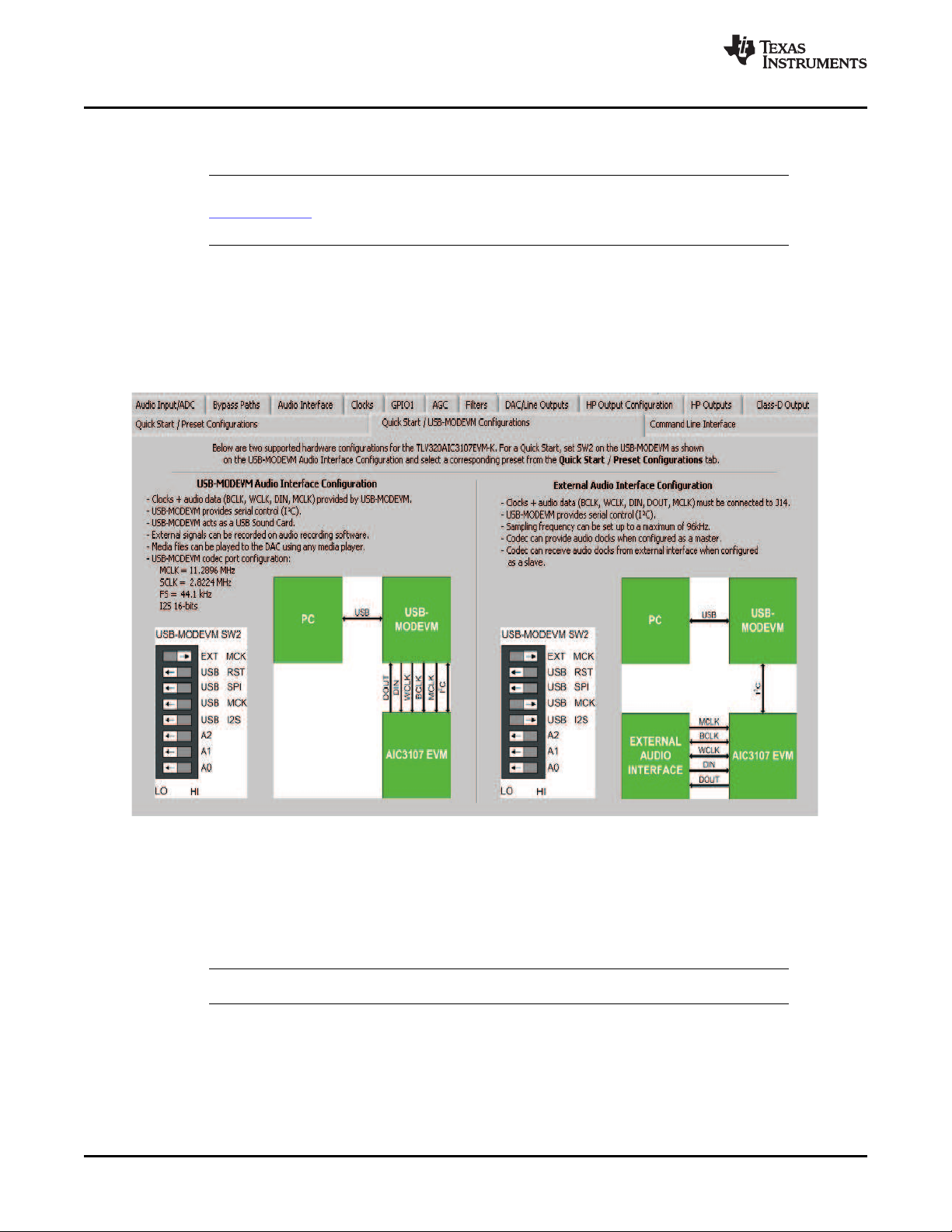
The Quick Start USB-MODEM Configurations tab and The Quick Start Preset Configurations tab Figure 3
helps the user to begin using the GUI.
4.1.1 Quick Start - USB-MODEM Configurations
www.ti.com
Figure 2. Quick Start - USB-MODEM Configurations
The default tab is the Quick Start - USB-MODEVM tab. This tab shows two common USB-MODEVM
configurations used with the AIC3107EVM. The default configuration is the USB-MODEVM Audio Interface
Configuration. In this configuration, the USB-MODEVM acts as a USB sound card. Audio files can be
played on the PC and targeted to the USB-MODEVM via the USB connection. On the USB-MODEVM, the
TAS1020B converts the USB audio to I2S data and the I2C script data to I2C commands.
Note: For correct EVM operation, ensure that SW2 switch settings are as shown in Figure 2 .
TLV320AIC3107EVM-K 8 SLAU261 – November 2008
Submit Documentation Feedback
Page 9
www.ti.com
4.1.2 Quick Start - Preset Configurations
TLV320AIC3107EVM Software
Figure 3. Quick Start - Preset Configurations Tab
The Quick Start Preset Configurations tab provides several different preset configurations of the codec
(Figure 3 ). The Preset Configurations buttons allow the user to choose from the provided defaults. When
the selection is made, the Preset Configuration Description shows a summary of the codec setup
associated with the choice made. If the choice is acceptable, the Load button can be pressed, and the
preset configuration is loaded into the codec. The user can change to the Command Line Interface tab
(see Figure 30 ) to view the actual settings that were programmed into the codec. Note that the controls of
the GUI are updated per any downloaded script whether it be a Preset Configuration script or a User
Script run form the Command Line Interface tab.
SLAU261 – November 2008 TLV320AIC3107EVM-K 9
Submit Documentation Feedback
Page 10
TLV320AIC3107EVM Software
4.2 Main Software Screen With Indicators and Functions
www.ti.com
Figure 4. Main Software Screen
Figure 4 illustrates the main screen of the EVM software. The indicators and buttons located above the
tabbed section of the front page are visible regardless of which tab is currently being selected.
The firmware box indicates from where the firmware being used is operating. In this release, the firmware
is on the USB-MODEVM, so the user sees USB-MODEVM in the box labeled Located on:. The version of
the firmware appears in the Version box below this.
To the right, the next group box contains controls for resetting the TLV320AIC3107EVM. A software reset
can be done by writing to a register in the TLV320AIC3107EVM; this is accomplished by clicking the
button labeled Reset.
Near the Firmware box, the Device Connected LED is green when the EVM is connected. If the indicator
is red, the EVM is not properly connected to the PC. Disconnect the EVM, and verify that the drivers were
correctly installed. Then reconnect, and try restarting the software.
On the upper right portion of the screen are located several indicators which provide the status of various
portions of the TLV320AIC3107. Pressing the Indicator Updates button activates these indicators. These
indicators, as well as the other indicators on this panel, are updated only when the software's front panel
is inactive, once every 20 ms.
10 TLV320AIC3107EVM-K SLAU261 – November 2008
Submit Documentation Feedback
Page 11
www.ti.com
The ADC Overflow and DAC Overflow indicators illuminate when the overflow flags are set in the
TLV320AIC3107. Below these indicators are the AGC Noise Threshold Exceeded indicators that
illuminate when the AGC noise threshold is exceeded. To the far right of the screen, the Short Circuit
Detect indicators illuminate when a short-circuit condition is detected, if this feature has been enabled.
Below the short-circuit indicators, the AGC Gain Applied indicators use a bar graph to show the amount
of gain which has been applied by the AGC and indicators that illuminate when the AGC is saturated.
4.2.1 Detailed TLV320AIC3107 Block Diagram
TLV320AIC3107EVM Software
Figure 5.
To view the detailed block diagram, click on the "Show" button at the top left of the Main Software Screen
(Figure 4 ). This block diagram shows the details of the processing blocks of the TLV320AIC3107 including
the I2C registers associated with each block.
SLAU261 – November 2008 TLV320AIC3107EVM-K 11
Submit Documentation Feedback
Page 12
TLV320AIC3107EVM Software
4.3 Audio Input/ADC Tab
www.ti.com
Figure 6. Audio Input/ADC Tab
The Audio Input/ADC tab allows control of the analog input mixer and the ADC. The controls are
displayed to look similar to an audio mixing console (see Figure 6 ). Each analog input channel has a
vertical strip that corresponds to that channel. By default, all inputs are muted when the TLV320AIC3107
is powered up.
To route an analog input to the ADC:
1. Select the Input Mode button to correctly show if the input signal is single-ended ( SE) or
fully-differential ( Diff). Inputs that are single-ended must be made to the positive signal terminal.
2. Click on the button of the analog input channel that corresponds to the correct ADC. The caption of the
button changes to Active. Note that the user can connect some channels to both ADCs, whereas
others only connect to one ADC.
3. Adjust the Level control to the desired attenuation for the connected channel. This level adjustment
can be done independently for each connection.
The TLV320AIC3107 offers a programmable microphone bias that can either be powered down, set to 2
V, 2.5 V, or the power supply voltage of the ADC (AVDD_ADC). Control of the microphone bias (mic bias)
voltage is accomplished by using the Mic Bias pulldown menu button above the last two channel strips.
To use the onboard microphone, hardware jumpers W10 and W11 must be installed. Nothing must be
plugged into J9, in order for the mic bias settings in the software to take effect. Also, jumper W9 (Mic Bias
Sel) must be set to connect positions 2 and 3, so that MICBIAS is controlled by the TLV320AIC3107.
Also shown are controls for Weak Common Mode Bias. Enabling these controls results in unselected
inputs to the ADC channels to be weakly biased to the ADC common mode voltage.
Nearby are the controls for the ADC PGA, including the master volume controls for the ADC inputs. Each
channel of the ADC can be powered up or down as needed using the Power Up buttons. PGA
soft-stepping for each channel is selected using the pulldown menu control. The two large knobs set the
actual ADC PGA Gain and allow adjustment of the PGA gains from 0 dB to 59.5 dB in 0.5-dB steps
(excluding Mute). At the extreme counterclockwise rotation, the channel is muted. Rotating the knob
clockwise increases the PGA gain, which is displayed in the box directly above the volume control.
TLV320AIC3107EVM-K 12 SLAU261 – November 2008
Submit Documentation Feedback
Page 13
www.ti.com
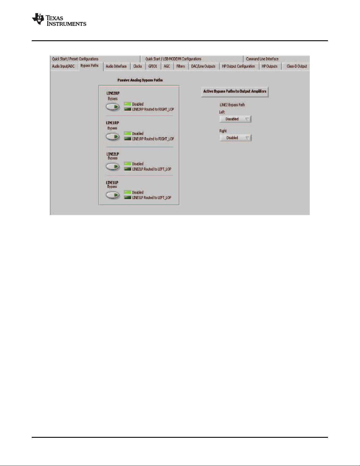
4.4 Bypass Paths Tab
TLV320AIC3107EVM Software
Figure 7. Bypass Paths Tab
As shown in Figure 7 , several analog bypass paths are available in the TMS320AIC3107. LINE1RP,
LINE2RP, LINE1LP, and LINE2LP inputs can be passively bypassed to either RIGHT_LOP or LEFT_LOP
by using the Passive Analog Bypass Paths controls. LINE2L (left) and LINE2R (right) buffered inputs
can directed to the output mixer sections by using the Active Bypass Paths to Output Amplifiers
controls.
SLAU261 – November 2008 TLV320AIC3107EVM-K 13
Submit Documentation Feedback
Page 14
TLV320AIC3107EVM Software
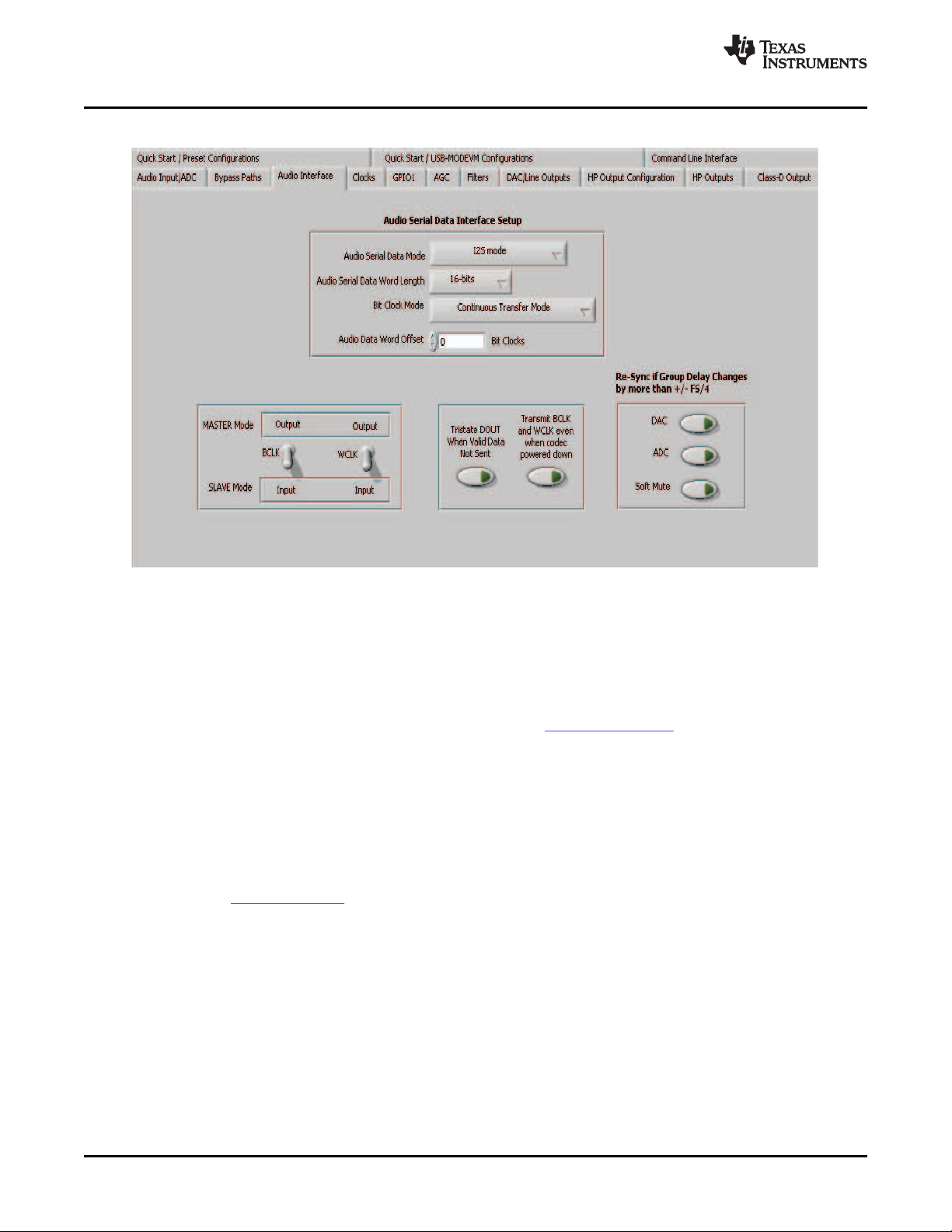
4.5 Audio Interface Tab
www.ti.com
Figure 8. Audio Interface Tab
The Audio Interface tab (Figure 8 ) allows configuration of the audio digital data interface to the
TLV320AIC3107.
The interface mode can be selected using the Audio Serial Data Mode control—selecting either I2S
mode, DSP mode, or Right- or Left-Justified modes. Word length can be selected using the Audio Serial
Word Length control, and the bit clock rate can also be selected using the Bit Clock Mode rate control.
The Audio Data Word Offset, used in TDM mode (see the product data sheet ) also can be selected on
this tab.
Along the bottom of this tab are controls for choosing the BLCK and WCLK as being either inputs or
outputs. With the codec configured in Slave mode, both the BCLK and WCLK are set to inputs. If the
codec is in Master mode, then BCLK and WCLK are configured as outputs. Additionally, two buttons
provide the options for 3-stating the DOUT line when no valid data is available and for transmitting BLCK
and WCLK when the codec is powered down.
Re-synchronization of the audio bus is enabled using the controls in the lower right corner of this screen.
Re-synchronization is done if the group delay changes by more than ± FS/4 for the ADC or DAC sample
rates (see the TLV320AIC3107 data sheet). The channels can be soft-muted when doing the
Re-synchronization if the Soft Mute button is enabled.
The default mode for the EVM is configured as 44.1-kHz, 16-bit, I2C words, and the codec is a slave
(BCLK and WCLK are supplied to the codec externally). For use with the PC software and the
USB-MODEVM, the default settings must be used; no changes to the software are required.
TLV320AIC3107EVM-K 14 SLAU261 – November 2008
Submit Documentation Feedback
Page 15
www.ti.com
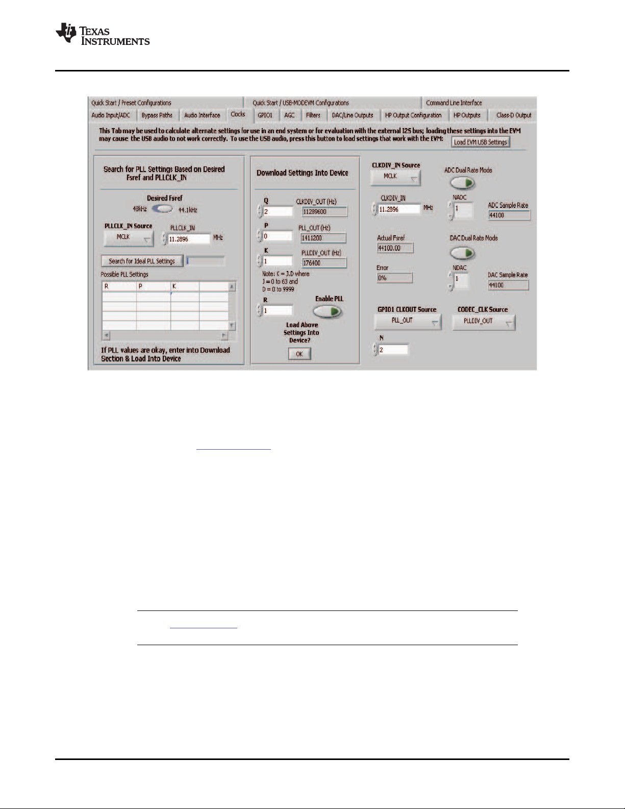
4.6 Clocks Tab
TLV320AIC3107EVM Software
The TLV320AIC3107 provides a phase-locked loop (PLL) that allows flexibility in the clock generation for
the ADC and DAC sample rates. The Clocks tab contains the controls that can be used to configure the
TLV320AIC3107 for operation with a wide range of master clocks. See the Audio Clock Generation
Processing figure in the TLV320AIC3107 data sheet for further details of selecting the correct clock
settings.
For use with the PC software and the USB-MODEVM, the clock settings must be set a certain way. If the
settings are changed from the default settings which allow operation from the USB-MODEVM clock
reference, the EVM settings can be restored automatically by clicking the Load EVM USB Settings
button. Note that changing any of the clock settings from the values loaded when this button is pushed
can result in the EVM not working properly with the PC software or USB interface. If an external audio bus
is used (audio not driven over the USB bus), then settings can be changed to any valid combination. See
Figure 9 .
4.6.1 Configuring the Codec Clocks and Fsref Calculation
The codec clock source is chosen by the CODEC_CLK Source control. When this control is set to
CLKDIV_OUT, the PLL is not used; when set to PLLDIV_OUT, the PLL is used to generate the clocks.
Note: Per the TLV320AIC3107 data sheet, the codec must be configured to allow the value of
Fsref to fall between the values of 39 kHz to 53 kHz.
Figure 9. Clocks Tab
SLAU261 – November 2008 TLV320AIC3107EVM-K 15
Submit Documentation Feedback
Page 16

TLV320AIC3107EVM Software
4.6.1.1 Use Without PLL
Setting up the TLV320AIC3107 for clocking without using the PLL permits the lowest power consumption
by the codec. The CLKDIV_IN source can be selected as either MCLK (default) or BCLK. The CLKDIV_IN
frequency then is entered into the CLKDIV_IN box, in megahertz (MHz). The default value shown,
11.2896 MHz, is the frequency used on the USB-MODEVM board. This value then is divided by the value
of Q, which can be set from 2 to 17; the resulting CLKDIV_OUT frequency is shown in the indicator next
to the Q control. The result frequency is shown as the Actual Fsref.
4.6.1.2 Use With PLL
When PLLDIV_OUT is selected as the codec clock source, the PLL is used. The PLL clock source is
chosen using the PLLCLK_IN control, and can be set to either MCLK or BCLK. The PLLCLK_IN
frequency then is entered into the PLLCLK_IN Source box.
The PLL_OUT and PLLDIV_OUT indicators show the resulting PLL output frequencies with the values set
for the P, K, and R parameters of the PLL. See the TLV320AIC3107 data sheet for an explanation of
these parameters. The parameters can be set by clicking on the up/down arrows of the P, K, and R
combination boxes, or they can be typed into these boxes.
Use the Search for PLL Settings Based on Desired Fsref and PLLCLK_IN section to find the ideal
values of P, K, and R for a given PLL input frequency and desired Fsref:
1. Set the desired Fsref using the Fsref switch.
2. Verify that the correct reference frequency is entered into the PLLCLK_IN Source box in megahertz
(MHz)
3. Push the Search for Ideal PLL Settings button. The software starts searching for ideal combinations
of P, K, and R, which achieve the desired Fsref. The possible settings for these parameters are
displayed in the spreadsheet-like table labeled Possible Settings.
4. Click on a row in this table to select the P, K, and R values located in that row. Notice that when this is
done, the software updates the P, K, R, PLL_OUT and PLLDIV_OUT readings, as well as the Actual
Fsref and Error displays. The values show the calculations based on the values that were selected.
This process does not actually load the values into the TLV320AIC3107, however; it only updates the
displays in the software. If more than one row exists, the user can choose the other rows to see which
of the possible settings comes closest to the ideal settings.
When a suitable combination of P, K, and R has been chosen, pressing the Load Settings into Device?
button downloads these values into the appropriate registers on the TLV320AIC3107.
www.ti.com
4.6.1.3 Setting ADC and DAC Sampling Rates
The Fsref frequency that determines either enabling or bypassing the PLL (see Section 4.6.1.1 or
Section 4.6.1.2 ) is used to determine the actual ADC and DAC sampling rates. By using the NADC and
NDAC factors, the sampling rates are derived from the Fsref. If the dual-rate mode is desired, this option
can be enabled for either the ADC or DAC by pressing the corresponding Dual Rate Mode button. The
ADC and DAC sampling rates are shown in the box to the right of each control.
TLV320AIC3107EVM-K 16 SLAU261 – November 2008
Submit Documentation Feedback
Page 17
www.ti.com
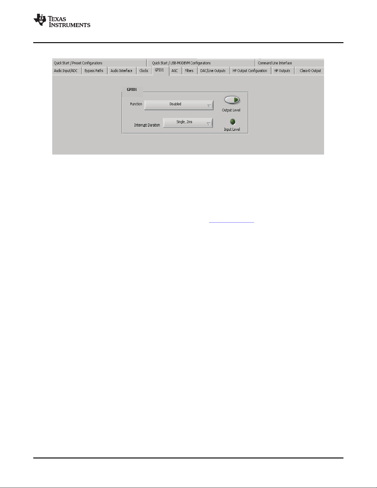
4.7 GPIO1 Tab
The GPIO1 tab (see Figure 10 ) selects options for the general-purpose inputs and outputs (GPIO) of the
TLV320AIC3107.
The GPIO1 groupbox contains controls for setting options for the GPIO1 pin. The Function control selects
the function of GPIO1 from the following:
• ADC Word Clock
• An output clock derived from the reference clock (see TLV320AIC3107 data sheet)
• Interrupt output pin to signal:
• Alternate I2S Word Clock
• A general-purpose I/O pin
TLV320AIC3107EVM Software
Figure 10. GPIO1 Tab
– Short Circuit
– AGC Noise Threshold detection
– Jack/Headset detection
• For use as an interrupt output, the behavior of the interrupt can be selected using the Interrupt
Duration control. A Single, 2ms pulse can be delivered when the selected interrupt occurs, or
Continuous Pulses can be generated signaling the interrupt.
– If selected as a General Purpose Input, the state of the GPIO1 pin is reflected by the Input Level
indicator. If selected as a General Purpose Output, the state of the GPIO1 pin can be set by using
the Output Level button.
SLAU261 – November 2008 TLV320AIC3107EVM-K 17
Submit Documentation Feedback
Page 18

TLV320AIC3107EVM Software
4.8 AGC Tab
www.ti.com
Figure 11. AGC Tab
The AGC tab (see Figure 11 ) consists of two identical sets of controls, one for the left channel and the
other for the right channel. The AGC function is described in the TLV320AIC3107 data sheet.
The AGC can be enabled for each channel using the Enable AGC button. Target gain, Attack time in
milliseconds, Decay time in milliseconds, and the Maximum PGA Gain Allowed can all be set,
respectively, using the four corresponding knobs in each channel.
The TLV320AIC3107 allows for the Attack and Decay times of the AGC to be setup in two different
modes, standard and advanced. The Left/Right AGC Settings button determines the mode selection.
The Standard mode provides several preset times that can be selected by adjustments made to the
Attackand Decay knobs. If finer control over the times is required, then the Advanced mode is selected to
change to the settings. When the Advanced mode is enabled, two tabs appear that allow separate,
advanced control of the Attack and Delay times of the AGC (see Figure 12 and Figure 13 ). These options
allow selection of the base time as well as a multiplier to achieve the actual times shown in the
corresponding text box. The Use advanced settings? button must be enabled to program the registers
with the correct values selected via the pulldown options for base time and multiplier.
18 TLV320AIC3107EVM-K SLAU261 – November 2008
Submit Documentation Feedback
Page 19

www.ti.com
TLV320AIC3107EVM Software
Figure 12. Left AGC Settings
Figure 13. Advanced
Noise gate functions, such as Hysteresis, Enable Clip stepping, Threshold (dB), Signal Detect
Debounce (ms), and Noise Detect Debounce (ms) are set using the corresponding controls in the
Noise Gate groupbox for each channel.
SLAU261 – November 2008 TLV320AIC3107EVM-K 19
Submit Documentation Feedback
Page 20

TLV320AIC3107EVM Software
4.9 Filters Tab
www.ti.com
Figure 14. Filters Tab
The TLV320AIC3107 has an advanced feature set for applying digital filtering to audio signals. This tab
controls all of the filter features of the TLV320AIC3107. In order to use this tab and have plotting of filter
responses correct, the DAC sample rate must be set correctly. Therefore, the clocks must be set up
correctly in the software following the discussion in Section 4.6 . See Figure 14 .
The AIC3107 digital filtering is available to both the ADC and DAC. The ADC has optional high-pass (HP)
filtering and allows the digital output from the ADC through digital effects filtering before exiting the codec
through the PCM interface. Likewise, the digital audio data can be routed through the digital effects
filtering before passing through the optional de-emphasis filter before the DAC. The digital effects filtering
can only be connected to either the ADC or DAC, not both at the same time.
The Figure 14 is divided into several areas. The left side of the tab, is used to select between the DAC or
ADC filters and to assist in the selection and calculating of the desired filter coefficients. The right side of
the tab shows a frequency response plot of the digital effects filter selected and the coefficients that are
programmed into the device. The plots show the magnitude and phase response of each biquad section,
plus the combined responses of the two biquad filters. Note that the plot shows only the responses of the
effect filters, not the combined response of those filter along with the de-emphasis and ADC high-pass
filters.
20 TLV320AIC3107EVM-K SLAU261 – November 2008
Submit Documentation Feedback
Page 21

www.ti.com
4.9.1 ADC Filters
4.9.1.1 High-Pass Filter
The TLV320AIC3107 ADC provides the option of enabling a high-pass filter, which helps to reduce the
effects of DC offsets in the system. The Figure 15 tab shows the options for programming various filter
associated with the ADC. The high-pass filter has two modes: standard and programmable.
The standard high-pass filter option (Figure 16 ) allows for the selection of the high-pass filter frequency
from several preset options that can be chosen with the Left ADC HP Filter and Right ADC HP Filter
controls. The four options for this setting are disabled or three different corner frequencies which are
based on the ADC sample rate.
TLV320AIC3107EVM Software
Figure 15. ADC High-Pass Filters
Figure 16. ADC High-Pass Filter Settings
For custom filter requirements, the programmable function allows custom coefficients to achieve a
different filter than provided by the preset filters. The controls for the programmable high-pass filter are
located under the Programmable Filters heading. The following steps describe the process:
1. Enter the filter coefficients in the HP Filter controls near the bottom of the tab.
2. Press the Download Coefficients button to download the coefficients to the codec registers.
3. Enable the Programmable High-Pass Filters by selecting the Left ADC and Right ADC buttons.
The programmable high-pass filter is now correctly programmed and enabled. The ADC can be enabled
with the high-pass filter.
4.9.1.2 Digital Effects Filter - ADC
The ADC digital outputs stream can be routed through the digital effects filter in the codec to allow custom
audio performance. The digital effects filter cannot operate on both the ADC or DAC at the same time.
The digital effects filter operation is discussed in Section 4.9.3
SLAU261 – November 2008 TLV320AIC3107EVM-K 21
Submit Documentation Feedback
Page 22

TLV320AIC3107EVM Software
4.9.2 DAC Filters
4.9.2.1 De-emphasis Filters
The de-emphasis filters used in the TLV320AIC3107 can be programmed as described in the
TLV320AIC3107 data sheet, using this tab (Figure 18 ). Enter the coefficients for the de-emphasis filter
response desired. While on this tab, the de-emphasis response is shown on the Effect Filter Response
graph; however, note that this response is not included in graphs of other effect responses when on other
filter design tabs.
www.ti.com
Figure 17. DAC Filters
4.9.2.2 DAC Digital Effects Filter
The digital audio input stream can be routed through the digital effects filter in the codec before routing to
the DAC to allow custom audio performance. The digital effects filter cannot operate on both the ADC or
DAC at the same time. The digital effects filter operation is discussed in Section 4.9.3
TLV320AIC3107EVM-K 22 SLAU261 – November 2008
Figure 18. De-emphasis Filters
Submit Documentation Feedback
Page 23

www.ti.com
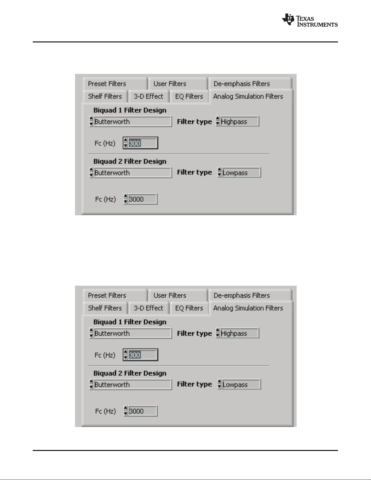
4.9.3 Digital Effects Filters
The digital effect filters (the biquad filters) of the TLV320AIC3107 are selected using the check boxes
shown in Figure 19 . The de-emphasis filters are described in the TLV320AIC3107 data sheet, and their
coefficients can be changed (see Figure 17 ).
When designing filters for use with TLV320AIC3107, the software allows for several different filter types to
be used. These options are shown on a tab control in the lower left corner of the screen. When a filter
type is selected, and suitable input parameters defined, the response are shown in the Effect Filter
Response graph. Regardless of the setting for enabling the Effect Filter, the filter coefficients are not
loaded into the TLV320AIC3107 until the Download Coefficients button is pressed. To avoid noise during
the update of coefficients, it is recommended that the user uncheck the Effect Filter enable check boxes
before downloading coefficients. Once the desired coefficients are in the TLV320AIC3107, enable the
Effect Filters by checking the boxes again.
4.9.3.1 Shelf Filters
A shelf filter is a simple filter that applies a gain (positive or negative) to frequencies above or below a
certain corner frequency. As shown in Figure 20 , in Bass mode a shelf filter applies a gain to frequencies
below the corner frequency; in Treble mode the gain is applied to frequencies above the corner frequency.
TLV320AIC3107EVM Software
Figure 19. Enabling Filters
Figure 20. Shelf Filters
To use these filters, enter the gain desired and the corner frequency. Choose the mode to use ( Bass or
Treble); the response is plotted on the Effect Filter Response graph.
SLAU261 – November 2008 TLV320AIC3107EVM-K 23
Submit Documentation Feedback
Page 24
TLV320AIC3107EVM Software
4.9.3.2 EQ Filters
EQ, or parametric, filters can be designed on this tab (see Figure 21 ). Enter a gain, bandwidth, and a
center frequency (Fc). Either bandpass (positive gain) or band-reject (negative gain) filters can be created
www.ti.com
4.9.3.3 Analog Simulation Filters
Biquads are good at simulating analog filter designs. For each biquad section on this tab, enter the
desired analog filter type to simulate (Butterworth, Chebyshev, Inverse Chebyshev, Elliptic, or Bessel).
Parameter entry boxes appropriate to the filter type are shown (ripple, for example, with Chebyshev filters,
etc.). Enter the desired design parameters, and the response is shown ( Figure 22 ).
Figure 21. EQ Filters
Figure 22. Analog Simulation Filters
TLV320AIC3107EVM-K 24 SLAU261 – November 2008
Submit Documentation Feedback
Page 25

www.ti.com
4.9.3.4 Preset Filters
Many applications are designed to provide preset filters common for certain types of program material.
This tab (see Figure 23 ) allows selection of one of four preset filter responses - Rock, Jazz, Classical, or
Pop.
TLV320AIC3107EVM Software
4.9.3.5 User Filters
If filter coefficients are known, they can be entered directly on this tab (see Figure 24 ) for both biquads for
both left and right channels. The filter response is not shown on the Effect Filter Response graph for user
filters.
Figure 23. Preset Filters
Figure 24. User Filters
SLAU261 – November 2008 TLV320AIC3107EVM-K 25
Submit Documentation Feedback
Page 26

TLV320AIC3107EVM Software
4.9.3.6 3D Effect
The 3D effect is described in the TLV320AIC3107 data sheet. It uses the two biquad sections differently
than most other effect filter settings. To use this effect properly, ensure that the appropriate coefficients
are already loaded into the two biquad sections. The User Filters tab can be used to load the coefficients.
See Figure 25 .
www.ti.com
To enable the 3D effect, check the 3D Effect On box. The Depth knob controls the value of the 3D
Attenuation Coefficient.
4.10 DAC/Line Outputs Tab
Figure 25. 3D Effect Settings
Figure 26. DAC/Line Outputs Tab
26 TLV320AIC3107EVM-K SLAU261 – November 2008
Submit Documentation Feedback
Page 27

www.ti.com
The DAC/Line Outputs tab controls the DAC power and volume, as well as routing of digital data to the
DACs and the analog line output from the DACs. (See Figure 26 .)
4.10.1 DAC Controls
On the left side of this tab are controls for the left and right DACs.
In similar fashion as the ADC, the DAC controls are set up to allow powering of each DAC individually and
setting the output level. Each channel's level can be set independently using the corresponding Volume
knob. Alternately, by checking the Slave to Right box, the left-channel Volume can be made to track the
right-channel Volume knob setting; checking the Slave to Left box causes the right-channel Volume knob
to track the left-channel Volume knob setting.
Data going to the DACs is selected using the drop-down boxes under the Left and Right DAC Datapath.
Each DAC channel can be selected to be off, use left-channel data, use right-channel data, or use a mono
mix of the left and right data.
Analog audio coming from the DACs is routed to outputs using the Output Path controls in each DAC
control panel. The DAC output can be mixed with the analog inputs (LINE2L, LINE2R, PGA_L, PGA_R)
and routed to the Line or High Power outputs using the mixer controls for these outputs on this tab (for the
line outputs) or on the High Power Outputs tab (for the high power outputs). If the DAC is to be routed
directly to either the Line or HP outputs, these can be selected as choices in the Output Path control.
Note that if the Line or HP outputs are selected as the Output Path, the mixer controls on this tab and the
High Power Output tabs have no effect.
4.10.2 Line Output Mixers
On the right side of this tab are horizontal panels where the analog output mixing functions for the line
outputs are located.
Each line output master volume is controlled by the knob at the far right of these panels, below the line
output labels. The output amplifier gain can be muted or set at a value between 0 and 9 dB in 1-dB steps.
Power/Enabled status for the line output can also be controlled using the button below this master output
knob ( Powered Up).
If the DAC Output Path control is set to Mix with Analog Inputs, the six knobs in each panel can be used
to set the individual level of signals routed and mixed to the line output. LINE2L, LINE2R, PGA_L, PGA_R,
and DAC_L and DAC_R levels can each be set to create a custom mix of signals presented to that
particular line output. Note: if the DAC Output Path control is set to anything other than Mix with Analog
Inputs, these controls have no effect.
TLV320AIC3107EVM Software
SLAU261 – November 2008 TLV320AIC3107EVM-K 27
Submit Documentation Feedback
Page 28

TLV320AIC3107EVM Software
4.11 HP Output Stage Configuration Tab
www.ti.com
Figure 27. Output Stage Configuration Tab
The HP Output Stage Configuration tab (Figure 27 ) allows for setting various features of the output
drivers.
The Headset Configuration control can be set as either Fully-Differential or Pseudo-Differential. This
control is used to determine if the output stage is being used to drive a fully differential output load or a
output load where one of the outputs is referenced to a common-mode voltage (pseudo-differential).
The output Coupling control can be chosen as either Capless, that is capacitor less, (EVM
SW2-CAPLESS) or AC-coupled (EVM SW2-CAP). This setting corresponds to the setting of the hardware
switch (SW2) on the TLV320AIC3107EVM.
The common-mode voltage of the outputs can be set to 1.35V, 1.5V, 1.65V, or 1.8V using the Common
Mode Voltage control.
The TLV320AIC3107 offers several options to help reduce the turn-on/off pop of the output amplifiers. The
Power-On Delay of the output drivers can be set using the corresponding control from 0 µ s up to 4 µ s.
Ramp-Up Step Timing also can be adjusted from 0 ms to 4 ms. The outputs can be set to soft-step their
volume changes, using the Output Volume Soft Stepping control, and set to step once per Fs period,
once per two Fs periods, or soft-stepping can be disabled altogether.
The high power outputs of the TLV320AIC3107 can be configured to go to a weak common-mode voltage
when powered down. The source of this weak common-mode voltage can be set on this tab with the
Weak Output CM Voltage Source drop-down menu. Choices for the source are either a resistor divider
off the AVDD_DAC supply, or a bandgap reference. See the data sheet for more details on this option.
Headset detection features are enabled using the Enable button in the HP Headset Detection groupbox.
When enabled, the indicators in the HS/Button Detect groupbox illuminate when either a button press or
headset is detected. When a headset is detected, the type of headset is displayed in the Detection Type
indicator. Debounce times for detection are set using the Jack Detect Debounce and Button Press
Debounce controls, which offer debounce times in varying numbers of milliseconds. See the
TLV320AIC3107 data sheet for a discussion of headset detection.
Output short-circuit protection can be enabled in the HP Short Circuit Protection groupbox. Short Circuit
Protection can use a current-limit mode, where the drivers limit current output if a short-circuit condition is
detected, or in a mode where the drivers power down when such a condition exists.
TLV320AIC3107EVM-K 28 SLAU261 – November 2008
Submit Documentation Feedback
Page 29
www.ti.com
4.12 HP Outputs Tab
TLV320AIC3107EVM Software
Figure 28. High Power Outputs Tab
This tab contains four horizontal groupings of controls, one for each of the high power outputs. Each
output has a mixer to mix the LINE2L, LINE2R, PGA_L, PGA_R, DAC_L and DAC_R signals, assuming
that the DACs are not routed directly to the high power outputs (see Section 4.10 ).
At the left of each output strip is a Powered Up button that controls whether the corresponding output is
powered up or not. The When powered down button allows 3-state outputs or driven weakly to a the
output common-mode voltage.
The HPxCOM outputs ( HPLCOM and HPRCOM) can be used as independent output channels or can be
used as complementary signals to the HPLOUT and HPROUT outputs. In these complementary
configurations, the HPxCOM outputs can be selected as Differential of HPxOUT signals to the
corresponding outputs or can be set to be a common-mode voltage ( Constant VCM Out. When used in
these configurations, the Powered Up button for the HPxCOM output is disabled, as the power mode for
that output tracks the power status of the HPL or HPR output that the COM output is tracking.
The HPRCOM Config selector allows a couple additional options compared to the HPLCOM Config
selector. Differential of HPLCOM allows the HPRCOM to be the complementary signal of HPLCOM for
driving a differential load between the HPxCOM outputs. The selector also allows Ext.
Feedback/HPLCOM constant VCM as an option. This option is used when the high power outputs are
configured for Capless output drive, where HPLCOM is configured as Constant VCM Out. The feedback
option provides feedback to the output and lowers the output impedance of HPLCOM.
At the right side of the output strip is a master volume knob for that output, which allows the output
amplifier gain to be muted or set from 0 to 9 dB in 1-dB steps.
SLAU261 – November 2008 TLV320AIC3107EVM-K 29
Submit Documentation Feedback
Page 30

TLV320AIC3107EVM Software
4.13 Class-D Output Tab
www.ti.com
Figure 29. Class-D Output Tab
The integrated Class-D speaker amplifier can drive one watt into an 8- Ω load. Figure 29 shows the
controls for the Class-D amplifier. The input to the Class-D amplifier is the same signal available at the left
lineout LEFT_LOP pin. The Class-D amplifier must be enabled first and then the gain control (0 dB to +18
dB) can be used. Note that many other gains are available in the signal path leading up to the Class-D
amplifier.
Also available is the an analog bypass switch to allow a signal up to 3.3 V to be input at SWINP and
SWINM and output at SWOUTP and SWOUTM. When the bypass switch is enabled (Register 76, D1), it
is also recommended to enable the Bypass Switch Bootstrap Clock (Register 76, D0).
TLV320AIC3107EVM-K 30 SLAU261 – November 2008
Submit Documentation Feedback
Page 31
www.ti.com
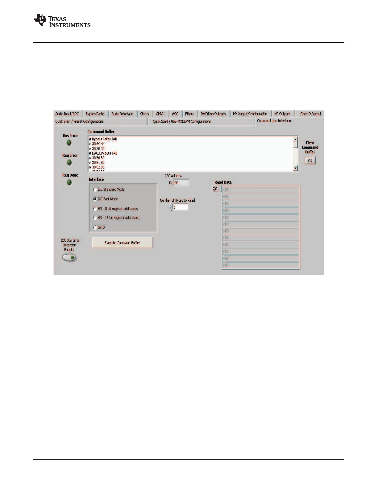
4.14 Command Line Interface Tab
A simple scripting language controls the TAS1020 on the USB-MODEVM from the LabView™-based PC
software. The main program controls, described previously, do nothing more than write a script which is
then handed off to an interpreter that sends the appropriate data to the correct USB endpoint. Because
this system is script based, provision is made in this tab for the user to view the scripting commands
created as the controls are manipulated, as well as load and execute other scripts that have been written
and saved (see Figure 30 ). This design allows the software to be used as a quick test tool or to help
provide troubleshooting information in the rare event that the user encounters problem with this EVM.
TLV320AIC3107EVM Software
Figure 30. Command Line Interface Tab
A script is loaded into the command buffer, either by operating the controls on the other tabs or by loading
a script file. When executed, the return packets of data which result from each command are displayed in
the Read Data array control. When executing several commands, the Read Data control shows only the
results of the last command. To see the results after every executed command, use the logging function
described in the following text.
The File menu (Figure 31 ) provides some options for working with scripts. The first option, Open
Command File..., loads a command file script into the command buffer. This script then can be executed
by pressing the Execute Command Buffer button.
The second option is Log Script and Results..., which opens a file save dialog box. Choose a location for a
log file to be written using this file save dialog. When the Execute Command Buffer button is pressed, the
script runs, and the script along with resulting data read back during the script, is saved to the file
specified. The log file is a standard text file that can be opened with any text editor and looks much like
the source script file, but with the additional information of the result of each script command executed.
The third menu item is a submenu of Recently Opened Files. This is simply a list of script files that have
previously been opened, allowing fast access to commonly used script files. The final menu item is Exit,
which terminates the TLV320AIC3107EVM software.
SLAU261 – November 2008 TLV320AIC3107EVM-K 31
Submit Documentation Feedback
Page 32

TLV320AIC3107EVM Software
Under the Help menu is an About... menu item which displays information about the TLV320AIC3107EVM
software.
The I2C Bus Error Detection button allows the user to enable circuitry which sets a register bit (Register
107, D0) if an I2C bus error is detected. It is unnecessary to use this with the GUI software but can be
used as part of error detection in the end-equipment software design.
The actual USB protocol used as well as instructions on writing scripts are detailed in the following
subsections. Although it is unnecessary to understand or use either the protocol or the scripts directly,
understanding them may be helpful to some users.
www.ti.com
Figure 31. File Menu
32 TLV320AIC3107EVM-K SLAU261 – November 2008
Submit Documentation Feedback
Page 33

www.ti.com
Appendix A EVM Connector Descriptions
This appendix contains the connection details for each of the main header connectors on the EVM.
A.1 Analog Interface Connectors
A.1.1 Analog Input/Output Connectors
In addition to the analog headers, the analog inputs and outputs also can be accessed through alternate
connectors, either screw terminals or audio jacks. The stereo microphone input is also tied to J6 and the
stereo headphone output (the HP set of outputs) is available at J7.
Table A-1 summarizes the analog input/output connectors available for Block A.
Designator Description Function PIN 1 PIN 2 PIN3
J6 3-Conductor Screw See SW1 Configuration for LINE1LP AGND LINE1LM
J7 3-Conductor Screw See SW1 Configuration for LINE1RP AGND LINE1RM
J8 3-Conductor Screw See SW1 Configuration for LINE2LP AGND LINE2LM
J9 Audio 3.5mm Stereo Input External Mic Input (See SW1 AGND MIC3L MIC3R
J10 Audio 3.5mm Stereo Headset Output (See SW2 AGND HPLOUT HPROUT
J11 Audio 3.5mm Stereo Headset Test Output (See AGND HPL-TEST HPR-TEST
J12 3-Conductor Screw Lineout LEFT_LOP AGND RIGHT_LOP
J15 2-Conductor Screw External SVDD (Class-D Class-D Voltage SPGND (ground) NA
J16 2-Conductor Screw Switchable Analog Inputs SWINM SWINP NA
J17 2-Conductor Screw Class-D Speaker Test OUT-M (filtered) OUT-P (filtered) NA
J18 2-Conductor Screw Class-D Speaker Output SPOM SPOP NA
Appendix A
Table A-1. Analog Input/Output Connectors
Terminal Input SE/Diff Usage
Terminal Input SE/Diff Usage
Terminal Input SE/Diff Usage
Jack Configuration)
Output Jack Configuration)
Output Jack SW2 Configuration) (filtered) (filtered)
Terminal Output
Terminal Input Power) (SVDD)
Terminal Input
Terminal Output
Terminal Output
SLAU261 – November 2008 EVM Connector Descriptions 33
Submit Documentation Feedback
Page 34

Block A and Block B Digital Interface Connectors (J16 and J17)
A.2 Block A and Block B Digital Interface Connectors (J16 and J17)
The TLV320AIC3107EVM is designed to easily interface with multiple control platforms. Samtec part
numbers SSW-110-22-F-D-VS-K and TSM-110-01-T-DV-P provide a convenient 10-pin dual row
header/socket combination at J16 and J17. These headers/sockets provide access to the digital control
and serial data pins of the device. Consult Samtec at www.samtec.com or call 1-800- SAMTEC-9 for a
variety of mating connector options. Table A-2 summarizes the digital interface pinout for the
TLV320AIC3107EVM.
Table A-2. Block A and Block B Digital Interface Pinout
Pin Number Signal Description
P4.1 NC Not Connected
P4.2 NC Not Connected
P4.3 NC Not Connected
P4.4 DGND Digital Ground
P4.5 NC Not Connected
P4.6 GPIO1 General Purpose Input/Output
P4.7 NC Not Connected
P4.8 RESET INPUT Reset signal input to AIC3107EVM
P4.9 NC Not Connected
P4.10 DGND Digital Ground
P4.11 NC Not Connected
P4.12 NC Not Connected
P4.13 NC Not Connected
P4.14 RESET Reset
P4.15 NC Not Connected
P4.16 NC Not Connected
P4.17 NC Not Connected
P4.18 DGND Digital Ground
P4.19 NC Not Connected
P4.20 NC Not Connected
P5.1 NC Not Connected
P5.2 NC Not Connected
P5.3 BCLK Audio Serial Data Bus Bit Clock (Input/Output)
P5.4 DGND Digital Ground
P5.5 NC Not Connected
P5.6 NC Not Connected
P5.7 WCLK Audio Serial Data Bus Word Clock (Input/Output)
P5.8 NC Not Connected
P5.9 NC Not Connected
P5.10 DGND Digital Ground
P5.11 DIN Audio Serial Data Bus Data Input (Input)
P5.12 NC Not Connected
P5.13 DOUT Audio Serial Data Bus Data Output (Output)
P5.14 NC Not Connected
P5.15 NC Not Connected
P5.16 SCL I2C Serial Clock
P5.17 MCLK Block A Master Clock Input
P5.18 DGND Digital Ground
P5.19 NC Not Connected
P5.20 SDA I2C Serial Data Input/Output
www.ti.com
EVM Connector Descriptions34 SLAU261 – November 2008
Submit Documentation Feedback
Page 35

www.ti.com
Note that P5 comprises the signals needed for an I2S serial digital audio interface; the control interface
(I2C and RESET) signals are routed to P4. I2C is actually routed to both connectors; however, the device
is connected only to P4.
A.3 Power Supply Connector Pin Header, J15
J15 provides connection to the common power bus for the TLV320AIC3107EVM. Power is supplied on the
pins listed in Table A-3 .
Table A-3. Power Supply Pinout
DVDD (1.8V) J15.7 J15.8 NC
IOVDD (3.3V) J15.9 J15.10 NC
The TLV320AIC3107EVM-K motherboard (the USB-MODEVM Interface board) supplies power to J15 of
the TLV320AIC3107EVM. Power for the motherboard is supplied either through its USB connection or via
terminal blocks on that board.
Power Supply Connector Pin Header, J15
Signal Pin Number Signal
NC J15.1 J15.2 NC
+5VA J15.3 J15.4 NC
DGND J15.5 J15.6 AGND
SLAU261 – November 2008 EVM Connector Descriptions 35
Submit Documentation Feedback
Page 36

SDA
D
IN
SWINM
MCLK
AVDD_DAC
D
OUT
SPVDD
SPOM
SWINP SCL
MICBIAS
SPOP
GPIO
1
BCLK
WCLK
DVDD
MICDET/LINE1LM
LINE1RP
LINE1LP
RIGHT_LOP
AVDD_ADC
H
PCOM
DRVD
D1
HPLOUTHPROUT
LEF
T_LOP
DRVDD
2
MIC3L/LINE1RM
LINE2LP
MIC3R/LINE2RM
LINE2RP/LINE2LM
R3
2.2K
C24
0.1uF
C23
47uF
R2
220
123
W9
MICB
IASSEL
+
3.3VA
EXT MICIN
ON-BOARDMICROPHONE
C28
NI
R50R6
0
C25
0.1uF
R4
2.2K
1 2
W11
1 2
W10
C26, C27,and C28 are not
installed, butcan be used to filter
51342
J
9
SJ1
-3515-SMT
1
2
MK1
MD974
5APZ-F
C27NIC26
NI
R1
100K
SVD
D
C5
0.1u
F
C13
22uF
1 2
W5
SPGND
TP5
SPPVDD
+3.3
VA
TP4
AVDD_D
AC
C33
47nF
C3
4
47nF
R11
100
R12
100
C35
1.0uF
C36
1.0uF
123
J12
LINE O
UT
LOR
LOL
TP22
LOL
TP23
LOR
+
3.3VA
C1
0.
1uF
C9
10
uF
1
2
W1
TP9
MICDET/LINE1LM
TP1
AVDD_ADC
+3.3V
A
C
2
0.1uF
C
10
10uF
1
2
W2
TP
2
DRVDD1
+3.3VA
C3
0.1uF
C11
10uF
1
2
W3
TP3
DRVDD2
TP29
SPOP
TP28
SPOM
L1
0ohm
L2
0ohm
C41
N
I
C42
NI
SPGND
SPGND
C37
.022uF
R13
402
TP24
OM
SPGND
C38
.022uF
R14
402
TP25
OP
TP30
SWINM
TP31
SWINP
LINE1LM
LINE1L
P
123
J6
LINE1L
LINE1RP
LIN
E1RM
123
J7
LINE1R
C17
0.
1uF
C
18
0.1uF
C19
0.1uF
C20
0.1uF
MICDET/LINE1LM
LINE1RP
LINE1L
P
MIC
3L/LINE1RM
LINE2LP
MIC3R/L
INE2RM
LINE2RP/LINE2LM
LIN
E2LM
LIN
E2LP
123
J8
LINE2L
C21
0.1uF
C22
0.1uF
DOUT
BCL
K
WCLK
D
IN
MCLK
G
PIO1
S
CL
SDA
/RES
ET
542
36187
91110
12
S
W1
4PDT_ESW_EG4208
C7
0.
1uF
C15
1.
0uF
1
2
W7
TP7
DVD
D
C8
0.1uF
C1
6
10uF
1
2
W8
TP8
IO
VDD
TP21
HP
ROUT
TP19
HPLOUT
C31
47nF
12
W12
R7
10
0
R9
16
C32
47nF
12
W13
R8
10
0
R10
16
HPR
HPL
+1.8VD
IOVDD
T
P10
LINE1LP
TP1
1
LI
NE1RP
TP12
MIC
3L/LINE1RM
TP13
LINE2LP
TP
14
LINE2R
P/LINE2LM
TP15
M
IC3R/LINE2RM
TP16
MICBIAS
TP32
SDA
TP33
SCL
TP
34
DOU
T
TP3
5
DIN
TP36
WC
LK
TP37
BCLK
TP38
MCLK
TP39
GPIO1
TP40
/RESET
UP
DOWN
DIF
FSE
LINE
1LPLINE
1LP
LINE1LM
LINE1RP
LINE1RP
MIC3R
LINE1RM
MIC3L
LINE2LP
LINE2LP
LINE2LM
LINE2RP
J6
J7
J8
SW1
HPLOUTHPCOM
HPROUT
C30
47uF
C29
47uF
HEADSETOUTPUT
542
36187
91110
12
SW
2
4PDT_ESW_EG4208
51342
J10
SJ1-351
5-SMT
TP18
HPR-TE
ST
TP17
HPL-TE
ST
TP20
HPCOM
C4
0.1u
F
C12
10uF
1 2
W4
51342
J11
SJ1
-3515-SMT
HEADSETTEST
(+)
(
-)
(+)
(-)
(+)
(-)
L
1/C41& L2/C42 are LC
filters that can be
populate
d to filter niose
after
removing the0 ohm
shunt resistors.
SCL
1
SDA
2
LINE1RP
5
AVSS_ADC
11
MICBIAS
10
MIC3R/LINE2RM
9
LINE2RP/LINE2LM
8
LINE2LP
7
MIC3L/LINE1RM
6
LINE1LP
4
MICDET/LINE1LM
3
IOVDD
40
DV
SS
39
DOUT
38
D
IN
37
WCLK
36
BCL
K
35
MCLK34DVDD
33
GPIO1
32
RESETZ
31
SWINP
30
SWOUTP
29
SWOUTM
28
SWINM
27
SPOP
26
SPVDD
25
SPVSS
24
SPOM
23
AVSS_DAC
22
RIGHT_LOP20LEFT_LOP19DRVDD18HPROUT17DRV
SS
16
HPCOM15H
PLOUT
14
DRVDD13AV
DD_ADC
12
AVDD_DAC
21
PPAD
0
U1
TLV
320AIC3107IRSB
1
2
J
17
SPEA
KERTEST
1
2
J18
SPEAKEROUTPUT
1
2
J16
SWIN
SWINP
SWINM
SWOUTP
SWOUTM
1
2
W18
SPOMSEL
1
2
W19
SPOPSEL
Appendix B
Appendix B TLV320AIC3107EVM Schematic
The schematic diagram for the modular TLV320AIC3107EVM is provided as a reference.
www.ti.com
36 TLV320AIC3107EVM Schematic SLAU261 – November 2008
Submit Documentation Feedback
Page 37

A
0(+)
2
A1(+)4A2(+)6A3(+)
8
A410A512A614A7
16
RE
F-
18
REF
+
20
A
0(-)
1
A1(-)3A2(-)5A3(-)7AGND9AGND11AG
ND
13
VCOM15AG
ND
17
AGN
D
19
J1
DAUGHTER-ANALOG
-
VA
2
-5VA
4
AGND
6
VD1
8
+5VD
10
+
VA
1
+5VA3DGND5+1.8VD7+3.3VD
9
J3
DAUGHTER-POWER
G
PIO0
2
DGND
4
GPIO16GPIO2
8
DGND
10
GPIO312GP
IO4
14
SCL
16
DG
ND
18
SDA
20
C
NTL
1
CLKX3CLKR5FSX7FSR9DX11DR13INT15TO
UT
17
GPIO
5
19
J4
DAUGHTER-SERIAL
MCLK
DIN
DOUTWCLK
BCLK
/RE
SET
SDA
SCL
J1(BOTTOM)=SAMTEC-P/N:SSW-110-22-F-D-VS
P5 (T
OP)=SAMTEC-P/N: TSM-110-01-L-DV-P
J5(BOTTOM)=SAMTEC-P/N:SSW-110-22-F-D-VS
P4 (TOP)=SAMTEC-P/N: TSM-110-01-L-D
V
-P
J4(B
OTTOM)=SAMTEC-P/N:SSW-110-22-F-D
-V
S
P3 (TO
P)=SAMTEC -P/N:TSM-105-01-L-DV-P
J3(B
OTTOM)=SAMTEC-P/N:SSW-105-22-F-D
-V
S
+5V
A
A0(+)2A1(+)4A2(+)6A3(+)
8
A410A512A
6
14
A7
16
REF-
18
REF+
20
A0(-)1A1(-)3A2(-)5A3(-)7AG
ND
9
AGND11A
GND
13
VCOM15AGND17AGND
19
J2
D
AUGHTER-ANALOG
J2(
BOTTOM)=SAMTEC -P/N:SSW-110-22-F-D-VS-K
AGND
DGND
+
3.3VD
+1.8V
D
DIN
D
OUT
MCLK
SCL
SDA
GPIO0
2
DGND
4
GPIO16GPIO2
8
DG
ND
10
GPIO312G
PIO4
14
SCL
16
DGND
18
SDA
20
CNTL1CLKX3CLKR5FSX7FS
R
9
DX11D
R
13
INT15TOUT17GPIO5
19
J5
DAUGHTER-SERIAL
1
2
W
16
TP47
AG
ND
TP46
DG
ND
VIN
3
VOUT
2
GND
1
U
2
REG1117-3.3
C45
10uF
C46
0.1u
F
C47
10uF
+3.
3VA
IO
VDD
123
W14
IOV
DD
VCC8VSS
4
SDA
5
SCL
6
A0
1
A1
2
A2
3
WP
7
U3
24LC64I/SN
C48
0.1uF
R19
2.7K
1
2
W17
+3.3VD
BCLK
WCLK
TP41
+5VA
TP45
+1.8V
D
TP43
IOVDD
TP44
+3.3V
D
GPIO1
1
2
W15
R1
7
0
SPGND
R1
8
0
TP48
SP
GND
TP42
+3.3
VA
TP49
SVDD
C51
10uF
1
2
J15
EXT.SVDD
C52
0.1uF
+5VA
L5
SV
DD
C49
47uF
C50
47uF
2
1
3
SW3
B
ATT
SP
GND
P3/
P5/
P4/
www.ti.com
Appendix B
SLAU261 – November 2008 TLV320AIC3107EVM Schematic 37
Submit Documentation Feedback
Page 38

Appendix C
Appendix C TLV320AIC3107EVM Layout Views
www.ti.com
Figure C-1. Assembly layer
Figure C-2. Top Layer
38 TLV320AIC3107EVM Layout Views SLAU261 – November 2008
Submit Documentation Feedback
Page 39

www.ti.com
Appendix C
Figure C-3. Layer 3
Figure C-4. Layer 4
SLAU261 – November 2008 TLV320AIC3107EVM Layout Views 39
Submit Documentation Feedback
Page 40

Appendix C
www.ti.com
Figure C-5. Bottom Layer
TLV320AIC3107EVM Layout Views40 SLAU261 – November 2008
Submit Documentation Feedback
Page 41

www.ti.com
Appendix D TLV320AIC3107EVM Bill of Materials
The complete bill of materials for the modular TLV320AIC3107EVM is provided as a reference.
Table D-1. TLV320AIC3107EVM Bill of Materials
Item Qty Value Ref Des Description Vendor Part Number
No.
ATTENTION:
Alternate Resistor and Capacitor vendors may be used. In this case substitutions must have like descriptions.
All components should be RoHS compliant. Some part numbers may be either leaded or RoHS. Verify purchased components
PCB
1 1 N/A TLV320AIC3107_RSB_EVM_RevA_PWB Texas Instruments
RESISTORS
2 4 0 R5, R6, R17, R18 RES 0 Ω 1/10W 5% 0603 SMD Panasonic ERJ-3GEY0R00V
3 2 16 R9, R10 RES 16 Ω 1W 5% 2512 SMD Panasonic ERJ-1TYJ160U
4 4 100 R7, R8, R11, R12 RES 100 Ω 1/10W 1% 0603 SMD Panasonic ERJ-3EKF1000V
5 1 220 R2 RES 220 Ω 1/10W 1% 0603 SMD Yageo RC0603FR-07220RL
6 2 402 R13, R14 RES 402 Ω 1/10W 1% 0603 SMD Vishay/Dale CRCW0603402RFKEA
7 2 2.2K R3, R4 RES 2.2 k Ω 1/10W 5% 0603 SMD Panasonic ERJ-3GEYJ222V
8 1 2.7K R19 RES 2.7 k Ω 1/10W 5% 0603 SMD Panasonic ERJ-3GEYJ272V
9 1 100K R1 RES 100 k Ω 1/10W 1% 0603 SMD Panasonic ERJ-3EKF1003V
CAPACITORS
10 2 0.022 µ F C37, C38 CAP CER 0.022 µ F 50V X8R 10% 0603 TDK Corporation C1608X8R1H223K
11 4 0.047 µ F C31–C34 CAP 47000PF 25 V CERM X7R 0603 Panasonic ECJ-1VB1E473K
12 7 0.1 µ F C1–C5, C7, C8 CAP CER 0.10 µ F 6.3V X5R 10% 0402 TDK Corporation C1005X5R0J104K
13 11 0.1 µ F C17–C22, C24, CAP CER 0.1 µ F 25V X7R 0603 TDK Corporation C1608X7R1E104K
C25, C46, C48, C52
14 3 1.0uF C15, C35, C36 CAP CERAMIC 1 µ F 10V X5R 0603 Panasonic ECJ-BVB1A105K
15 5 10 µ F C9–C12, C16 CAP CERAMIC 10 µ F 6.3V X5R 0603 Panasonic ECJ-1VB0J106M
16 3 10 µ F C45, C47, C51 CAP CER 10UF 16V X5R 20% 1206 TDK Corporation C3216X5R0J106M
17 1 22 µ F C13 CAP CER 22UF 6.3V X5R 20% 0805 TDK Corporation C2012X5R0J226M
18 5 47 µ F C23, C29, C30, CAP CER 47 µ F 10V X5R 1210 Murata GRM32ER61A476KE20L
C49, C50
19 5 Not Installed C26–C41, C42 CAP 0603 N/A N/A
PASSIVES
20 1 600 L5 FERRITE CHIP 600 OHM 500MA 0805 TDK Corporation MMZ2012R601A
21 2 0 (0 Ω used L1, L2 RES ZERO OHM 1/4W 5% 1206 SMD Panasonic ERJ-8GEY0R00V
in place of
Ferrite)
INTEGRATED CIRCUITS
22 1 U1 Audio CODEC Texas Instruments TLV320AIC3107IRSB
23 1 U2 IC LDO REG 3.3V 800MA SOT-223 Texas Instruments REG1117-3.3
24 1 U3 64K I2C EEPROM MicroChip 24LC64-I/SN
MISCELLANEOUS ITEMS
25 4 J15– J18 Screw Terminal Block, 2 Position On Shore Technology ED555/2DS
26 4 J6–J8, J12 Screw Terminal Block, 3 Position On Shore Technology ED555/3DS
27 3 J9–J11 3.5mm Audio Jack, T-R-S, SMD CUI Inc. SJ1-3515-SMT
28 or alternate KobiConn 161-3335-E
29 2 P4, P5 20 Pin SMT Plug Samtec TSM-110-01-L-DV-P
30 4 J1, J2, J4, J5 20 pin SMT Socket Samtec SSW-110-22-F-D-VS-K
31 1 P3 10 Pin SMT Plug Samtec TSM-105-01-L-DV-P
32 1 J3 10 pin SMT Socket Samtec SSW-105-22-F-D-VS-K
33 9 W10–W13, 2 Position Jumper , 0 .1" spacing Samtec TSW-102-07-L-S
W15–W19
Appendix D
SLAU261 – November 2008 TLV320AIC3107EVM Bill of Materials 41
Submit Documentation Feedback
Page 42

Appendix D
Table D-1. TLV320AIC3107EVM Bill of Materials (continued)
Item Qty Value Ref Des Description Vendor Part Number
No.
34 7 W1–W5, W7, W8 Bus Wire (18–22 Gauge)
35 2 W9, W14 3 Position Jumper , 0 .1" spacing Samtec TSW-103-07-L-S
36 1 MK1 Omnidirectional Microphone Cartridge Knowles Acoustics MD9745APZ-F
or alternate Knowles Acoustics MD9745APA-1
37 2 SW1, SW2 SWITCH SLIDE 4PDT 30V RT ANGLE E-Switch EG4208
38 1 SW3 SWITCH SLIDE SPDT 30V.2A PC MNT E-Switch EG1218
39 13 Not TP1–TP5, TP7, TEST POINT PC MINI 0.040"D RED Keystone Electronics 5000
40 3 TP46–TP48 TEST POINT PC MULTI PURPOSE BLK Keystone Electronics 5011
41 30 Not TP9–TP25, TEST POINT PC MINI 0.040"D WHITE Keystone Electronics 5002
42 Installed N/A Header Shorting Block Samtec SNT-100-BK-T
Installed TP8, TP41–TP45,
TP49
Installed TP28–TP40
per test
procedure.
www.ti.com
TLV320AIC3107EVM Bill of Materials42 SLAU261 – November 2008
Submit Documentation Feedback
Page 43

www.ti.com
Appendix E USB-MODEVM Schematic
The schematic diagram for USB-MODEVM Interface Board (included in the TLV320AIC3107EVM-K) is
provided as a reference. It appears on the following page.
Appendix E
SLAU261 – November 2008 USB-MODEVM Schematic 43
Submit Documentation Feedback
Page 44
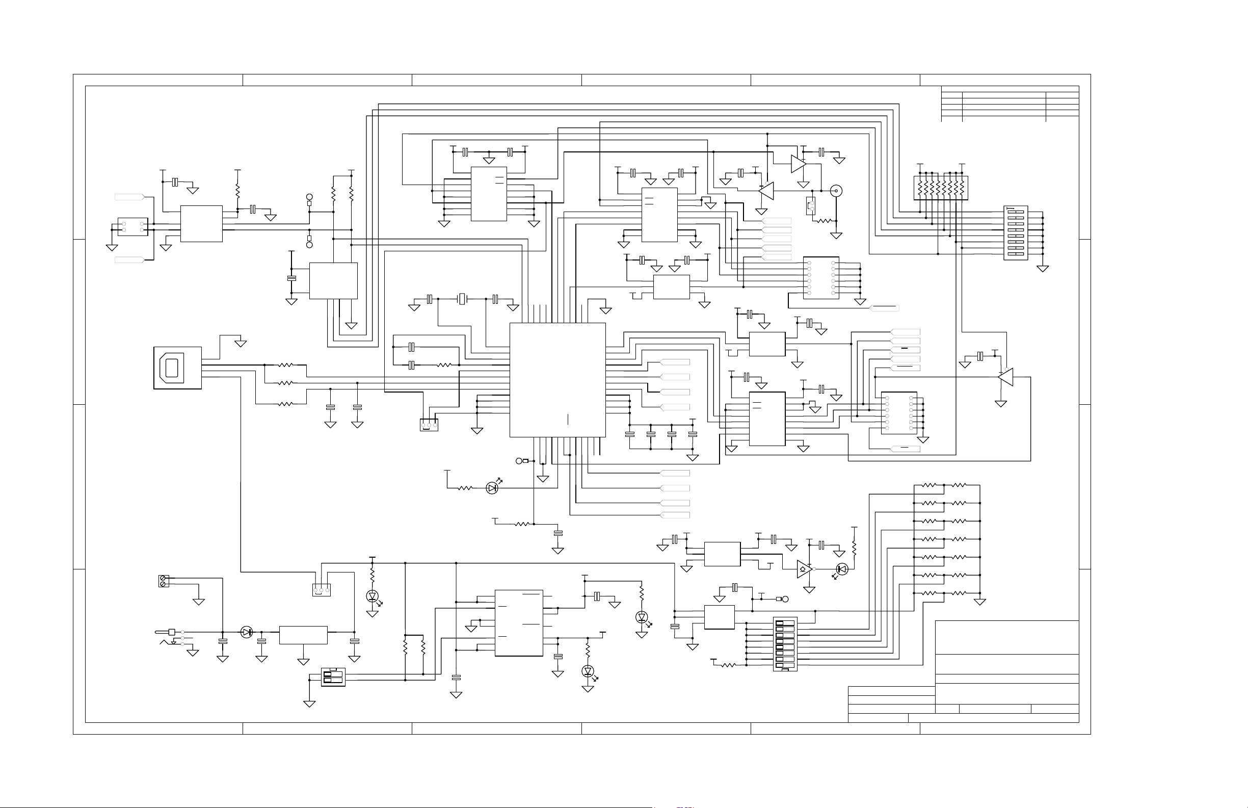
54321
REV ENGINEERING CHANGE NUMBER APPROVED
6
REVISION HISTORY
VCCB
OE1
OE2
1B1
1B2
2B1
2B2
C19
33pF
46
47
48
1
3
5
6
7
4
16
28
45
+3.3VD
U9
1IN
1IN
1EN
1GND
2GND
2EN
2IN
2IN
TPS767D318PWP
C33
0.1uF
+3.3VDIOVDD
16
15
14
13
12
11
10
9
44
XTALO
XTALI
PLLFILI
PLLFILO
MCLKI
PUR
DP
DM
DVSS
DVSS
DVSS
AVSS
TP11
MRESET
R17
100K
1RESET
2RESET
SCL
43
SDA
1OUT
1OUT
2OUT
2OUT
USB MCK
41
42
VREN
RESET
MRESET
TEST10EXTEN
9
37
40
CSCLK
MCLKO139MCLKO2
RSTO
P3.013P3.114P3.2/XINT15P3.317P3.418P3.5
11
12
28
24
23
22
18
17
C44
1uF
VCCA
DIR1
DIR2
1A1
1A2
2A1
2A2
GND
P1.3
P1.2
P1.1
P1.0
P3.5
P3.4
P3.3
P3.1-P3.2
C36
VCCA
0.1uF
C22
0.1uF
U3
GND
C11
0.1uF
C37
0.1uF
1
2
3
4
5
6
7
8
C23
0.1uF
A
+3.3VD
IOVDD
U5
IOVDD
1
3
2
C12
0.1uF
U13
1
VCCA
3
A
2
GND
SN74AVC1T45DBV
U14
1
IN
3
EN
2
GND
TPS73201DBV
IOVDD
+3.3VD
C34
0.1uF
16
VCCB
15
USB I2S
35
38
36
34
32
U8
TAS1020BPFB
CDATI
CSYNC
CDATO
CRESET
CSCHNE
31
P1.7
30
P1.6
29
P1.5
27
P1.4
26
P1.3
25
P1.2
24
P1.1
23
P1.0
8
DVDD
21
DVDD
33
DVDD
2
AVDD
NC20NC
22
19
+1.8VD
C7
10uF
+3.3VD
R19
220
C8
10uF
D4
SML-LX0603GW-TR
GREEN
+3.3VD
IOVDD
14
13
12
11
10
9
SN74AVC4T245PW
C35
0.1uF
6
4
5
C24
0.1uF
R4
10
SML-LX0603IW-TR
OE1
OE2
1B1
1B2
2B1
2B2
GND
VCCB
B
DIR
SN74AVC1T45DBV
C10
0.1uF
D5
RED
IOVDD
+3.3VD
VCCB
OUT
FB
R38
10M
C28
0.1uF
+3.3VD
6
4
5
SN74AVC1T45DBV
C43
0.1uF
16
15
14
13
12
11
10
9
B
DIR
C25
10uF
5
4
+3.3VD
53
SN74LVC1G125DBV
C42
0.1uF
VCCB
B
DIR
VCCB
OE1
OE2
1B1
1B2
2B1
2B2
GND
SN74AVC4T245PW
+3.3VDIOVDD
6
4
5
IOVDD
SN74LVC1G06DBV
IOVDD
1.2V
1.4V
1.6V
1.8V
2.0V
2.5V
3.0V
3.3V
C32
D
SDA
J6
EXTERNAL I2C
SCL
C
B
A
IOVDD
C30
0.1uF
U11
VREF12VREF2
241
3
4
SDA1
3
SCL1
1
GND
PCA9306DCT
USB SLAVE CONN
J7
897-30-004-90-000000
J8
ED555/2DS
EXT PWR IN
GND
VCC
D+
D-
6VDC-10VDC IN
J9
CUI-STACK PJ102-BH
2.5 MM
1 2 3 4 5 6
SDA2
SCL2
4
3
2
1
+3.3VD
R23
200k
C31
7
8
5
6
C15
0.1uF
DL4001
0.1uF
3
C16
0.33uF
EN
R9
1.5K
R10
27.4
R11
27.4
U2
REG1117-5D1
+3.3VD
VIN
TP9
TP10
8
C9
0.1uF
4
24LC64I/SN
PWR SELECT
GND
1
U1
VCC
VSS
JMP6
VOUT
+3.3VD
R3
2.7KR52.7K
5
SDA
A01A12A23WP
C13
47pF
123
2
SW1
REGULATOR ENABLE
6
SCL
7
C6
10uF
14
23
C14
47pF
+5VD
R14
390
SML-LX0603GW-TR
3.3VD ENABLE
1.8VD ENABLE
D3
GREEN
EXT MCK
C20
C21
.001uF
R15
10K
100pF
C18
33pF
123
JMP7
JPR-1X3
R16
10K
0.1uF
1
2
3
4
5
6
7
X1
MA-505 6.000M-C0
6.00 MHZ
R12
3.09K
+3.3VD
R13
649
C17
0.33uF
U12
VCCA
DIR1
DIR2
1A1
1A2
2A1
2A2
GND8GND
SN74AVC4T245PW
USB ACTIVE
D2
SML-LX0603YW-TR
YELLOW
5
6
4
3
9
10
11
12
2 4
1
U10
24
MCLK
I2SDIN
BCLK
LRCLK
I2SDOUT
U7
VCCA
A
GND
U4
VCCA
DIR1
DIR2
1A1
1A2
2A1
2A2
GND
C38
0.1uF
2 4
TP6
SW3
IOVDD SELECT
+3.3VD
C41
1
0.1uF
53
U15
SN74LVC1G126DBV
EXT MCLK
JMP8
JPR-2X1
R20
1 2
75
J14
1
3
5
7 8
9 10
11 12
EXTERNAL AUDIO DATA
IOVDD
C26
0.1uF
1
3
2
IOVDD
C27
1
0.1uF
2
3
4
5
6
7
8
USB SPI
+3.3VD
C39
0.1uF
53
U16
SML-LX0603GW-TR
89
710
611
512
413
314
215
116
J10
2
4
6
+3.3VD
R24
220
D8
GREEN
ENGINEER
DRAWN BY
DOCUMENT CONTROL NO.
SHEET OF FILE
PWR_DWN
MISO
MOSI
SCLK
RESET
J15
1
3
5
7 8
9 10
11 12
EXTERNAL SPI
RICK DOWNS
ROBERT BENJAMIN
12
+3.3VD
SS
2
4
6
INT
R25
22.1k
R27
25.5k
R29
28k
R31
32.4k
R33
39.2k
R35
46.4k
R37
52.3k
R26
137k
R28
76.8k
R30
56.2k
R32
48.7k
R34
36.5k
R36
30.9k
R18
30.1k
IOVDD
RA1
10K
A0
A1
A2
USB I2S
USB MCK
USB SPI
USB RST
EXT MCK
USB RST
C40
0.1uF
16
15
14
13
12
11
10
9
IOVDD
SW2
SW DIP-8
U17
1
53
SN74AUP1G125DBV
1
2
3
4
5
6
7
8
24
ti
DATA ACQUISITION PRODUCTS
HIGH PERFORMANCE ANALOG DIVISION
SEMICONDUCTOR GROUP
6730 SOUTH TUCSON BLVD., TUCSON, AZ 85706 USA
TITLE
USB-MODEVM INTERFACE
6463996
SIZE
DATE REV3-Apr-2007
B
C:\Work\USB-MODEVM\USB Motherboard - ModEvm.ddb - Docum ents\SCH\USB Interface
D
D
C
B
A
Page 45

54321
REV ENGINEERING CHANGE NUMBER APPROVED
6
REVISION HISTORY
D
123
J11
1
A0(-)
3
A1(-)
5
A2(-)
7
A3(-)
9
AGND
11
AGND
13
AGND
15
VCOM
17
AGND
19
AGND
DAUGHTER-ANALOG
J11A (TOP) = SAM_TSM-110-01-L-DV-P
J11B (BOTTOM) = SAM_SSW-110-22-F-D-VS-K
+5VA +5VD
JMP1
1 2
C
-5VA
C1
TP1 TP2 TP3
10uF
R21
390
J1
-5VA
D6
SML-LX0603GW-TR
GREEN
B
A
1 2 3 4 5 6
JPR-2X1
+5VA +5VD
C2
10uF
R22
390
J2
+5VA
D7
SML-LX0603GW-TR
GREEN
C3
10uF
J3
+5VD
J16
1
A0(-)
3
A1(-)
5
A2(-)
7
A3(-)
9
AGND
11
AGND
13
AGND
15
VCOM
17
AGND
19
AGND
DAUGHTER-ANALOG
J16A (TOP) = SAM_TSM-110-01-L-DV-P
J16B (BOTTOM) = SAM_SSW-110-22-F-D-VS-K
A0(+)
A1(+)
A2(+)
A3(+)
REF-
REF+
A0(+)
A1(+)
A2(+)
A3(+)
REF-
REF+
2
4
6
8
10
A4
12
A5
14
A6
16
A7
18
20
2
4
6
8
10
A4
12
A5
14
A6
16
A7
18
20
+1.8VD
J13A (TOP) = SAM_TSM-105-01-L-DV-P
+5VA
J13B (BOTTOM) = SAM_SSW-105-22-F-D-VS-K
J13
1
+VA
3
+5VA
5
DGND
7
+1.8VD
9
+3.3VD
DAUGHTER-POWER
TP7
AGND
JMP2
1 2
+1.8VD
J18
1
+VA
3
+5VA
5
DGND
7
+1.8VD
9
+3.3VD
DAUGHTER-POWER
+3.3VD
J4
+1.8VD
C4
10uF
TP5
+5VA
J18A (TOP) = SAM_TSM-105-01-L-DV-P
J18B (BOTTOM) = SAM_SSW-105-22-F-D-VS-K
-5VA
AGND
+5VD
-5VA
AGND
+5VD
VD1
VD1
-VA
-VA
TP8
DGND
-5VA
2
4
6
8
10
IOVDD
+5VD
TP4
+3.3VD
C5
10uF
J5
+3.3VD
2
-5VA
4
6
8
10
IOVDD
+5VD
J12
1
CNTL
3
CLKX
5
CLKR
7
FSX
9
FSR
11
DX
13
DR
15
INT
17
TOUT
19
GPIO5
DAUGHTER-SERIAL
J12A (TOP) = SAM_TSM-110-01-L-DV-P
J12B (BOTTOM) = SAM_SSW-110-22-F-D-VS-K
J17
1
CNTL
3
CLKX
5
CLKR
7
FSX
9
FSR
11
DX
13
DR
15
INT
17
TOUT
19
GPIO5
DAUGHTER-SERIAL
J17A (TOP) = SAM_TSM-110-01-L-DV-P
J17B (BOTTOM) = SAM_SSW-110-22-F-D-VS-K
GPIO0
DGND
GPIO1
GPIO2
DGND
GPIO3
GPIO4
SCL
DGND
SDA
1 2
GPIO0
DGND
GPIO1
GPIO2
DGND
GPIO3
GPIO4
SCL
DGND
SDA
IOVDD
JMP3
2
4
6
8
10
12
14
16
18
20
2
4
6
8
10
12
14
16
18
20
JMP5
IOVDD
RA2
10k
SCLK
SS
RESET
PWR_DWN
JMP4
1 2
R1
2.7K
R2
2.7K
MISO
MOSI
SCL
SDA
MCLK
I2SDOUT
I2SDIN
LRCLK
BCLK
IOVDD
IOVDD
INT
U6
1
2
3
4
5
6
7
8
9
10
11
SN74TVC3010PW
GND
A1
A2
A3
A4
A5
A6
A7
A8
A9
A10
A1112B11
GATE
+3.3VD
C29
R6
0.1uF
200k
24
23
B1
22
B2
21
B3
20
B4
19
B5
18
B6
17
B7
16
B8
15
B9
14
B10
13
R7
200k
R8
200k
P3.3
P3.4
P3.5
P1.0
P1.1
P1.2
P1.3
P3.1-P3.2
+3.3VD
ti
DATA ACQUISITION PRODUCTS
HIGH-PERFORMANCE ANALOG DIVISION
SEMICONDUCTOR GROUP
6730 SOUTH TUCSON BLVD., TUCSON, AZ 85706 USA
ENGINEER
RICK DOWNS
ROBERT BENJAMIN
DRAWN BY
DOCUMENT CONTROL NO. 6463996
SHEET OF FILE
22
TITLE
USB-MODEVM INTERFACE
SIZE
DATE REV3-Apr-2007
B
C:\Work\USB-MODEVM\USB Motherboard - ModEvm.ddb - Docum ents\SCH\Daughtercard Interface
D
D
C
B
A
Page 46

Appendix F
Appendix F USB-MODEVM Bill of Materials
The complete bill of materials for USB-MODEVM Interface Board (included only in the
TLV320AIC3107EVM-K)is provided as a reference.
Table F-1. USB-MODEVM Bill of Materials
Designators Description Manufacturer Mfg. Part Number
R4 10 Ω 1/10W 5% Chip Resistor Panasonic ERJ-3GEYJ1300V
R10, R11 27.4 Ω 1/16W 1% Chip Resistor Panasonic ERJ-3EKF27R4V
R20 75 Ω 1/4W 1% Chip Resistor Panasonic ERJ-14NF75R0U
R19 220 Ω 1/10W 5% Chip Resistor Panasonic ERJ-3GEYJ221V
R14, R21, R22 390 Ω 1/10W 5% Chip Resistor Panasonic ERJ-3GEYJ391V
R13 649 Ω 1/16W 1% Chip Resistor Panasonic ERJ-3EKF6490V
R9 1.5K Ω 1/10W 5% Chip Resistor Panasonic ERJ-3GEYJ1352V
R1–R3, R5–R8 2.7K Ω 1/10W 5% Chip Resistor Panasonic ERJ-3GEYJ272V
R12 3.09K Ω 1/16W 1% Chip Resistor Panasonic ERJ-3EKF3091V
R15, R16 10K Ω 1/10W 5% Chip Resistor Panasonic ERJ-3GEYJ1303V
R17, R18 100k Ω 1/10W 5%Chip Resistor Panasonic ERJ-3GEYJ1304V
RA1 10K Ω 1/8W Octal Isolated Resistor Array CTS Corporation 742C163103JTR
C18, C19 33pF 50V Ceramic Chip Capacitor, ± 5%, NPO TDK C1608C0G1H330J
C13, C14 47pF 50V Ceramic Chip Capacitor, ± 5%, NPO TDK C1608C0G1H470J
C20 100pF 50V Ceramic Chip Capacitor, ± 5%, NPO TDK C1608C0G1H101J
C21 1000pF 50V Ceramic Chip Capacitor, ± 5%, NPO TDK C1608C0G1H102J
C15 0.1 µ F 16V Ceramic Chip Capacitor, ± 10%, X7R TDK C1608X7R1C104K
C16, C17 0.33 µ F 16V Ceramic Chip Capacitor, ± 20%, Y5V TDK C1608X5R1C334K
C9–C12, C22–C28 1 µ F 6.3V Ceramic Chip Capacitor, ± 10%, X5R TDK C1608X5R0J1305K
C1–C8 10 µ F 6.3V Ceramic Chip Capacitor, ± 10%, X5R TDK C3216X5R0J1306K
D1 50V, 1A, Diode MELF SMD Micro Commercial Components DL4001
D2 Yellow Light Emitting Diode Lumex SML-LX0603YW-TR
D3– D7 Green Light Emitting Diode Lumex SML-LX0603GW-TR
D5 Red Light Emitting Diode Lumex SML-LX0603IW-TR
Q1, Q2 N-Channel MOSFET Zetex ZXMN6A07F
X1 6MHz Crystal SMD Epson MA-505 6.000M-C0
U8 USB Streaming Controller Texas Instruments TAS1020BPFB
U2 5V LDO Regulator Texas Instruments REG1117-5
U9 3.3V/1.8V Dual Output LDO Regulator Texas Instruments TPS767D318PWP
U3, U4 Quad, 3-State Buffers Texas Instruments SN74LVC125APW
U5–U7 Single IC Buffer Driver with Open Drain o/p Texas Instruments SN74LVC1G07DBVR
U10 Single 3-State Buffer Texas Instruments SN74LVC1G125DBVR
U1 Microchip 24LC64I/SN
TP1–TP6, TP9–TP11 Miniature test point terminal Keystone Electronics 5000
TP7, TP8 Multipurpose test point terminal Keystone Electronics 5011
J7 USB Type B Slave Connector Thru-Hole Mill-Max 897-30-004-90-000000
J13, J2–J5, J8 2-position terminal block On Shore Technology ED555/2DS
J9 2.5mm power connector CUI Stack PJ-102B
J130 BNC connector, female, PC mount AMP/Tyco 414305-1
J131A, J132A, J21A, J22A 20-pin SMT plug Samtec TSM-110-01-L-DV-P
J131B, J132B, J21B, J22B 20-pin SMT socket Samtec SSW-110-22-F-D-VS-K
J133A, J23A 10-pin SMT plug Samtec TSM-105-01-L-DV-P
J133B, J23B 10-pin SMT socket Samtec SSW-105-22-F-D-VS-K
J6 4-pin double row header (2x2) 0.1" Samtec TSW-102-07-L-D
J134, J135 12-pin double row header (2x6) 0.1" Samtec TSW-106-07-L-D
64K 2-Wire Serial EEPROM I2C
USB-MODEVM PCB Texas Instruments 6463995
www.ti.com
44 USB-MODEVM Bill of Materials SLAU261 – November 2008
Submit Documentation Feedback
Page 47

www.ti.com
Table F-1. USB-MODEVM Bill of Materials (continued)
Designators Description Manufacturer Mfg. Part Number
JMP1–JMP4 2-position jumper, 0.1" spacing Samtec TSW-102-07-L-S
JMP8–JMP14 2-position jumper, 0.1" spacing Samtec TSW-102-07-L-S
JMP5, JMP6 3-position jumper, 0.1" spacing Samtec TSW-103-07-L-S
JMP7 3-position dual row jumper, 0.1" spacing Samtec TSW-103-07-L-D
SW1 SMT, half-pitch 2-position switch C & K Division, ITT TDA02H0SK1
SW2 SMT, half-pitch 8-position switch C & K Division, ITT TDA08H0SK1
Jumper plug Samtec SNT-100-BK-T
Appendix F
SLAU261 – November 2008 USB-MODEVM Bill of Materials 45
Submit Documentation Feedback
Page 48
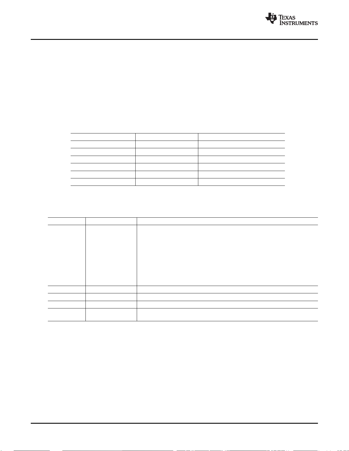
Appendix G
Appendix G USB-MODEVM Protocol
G.1 USB-MODEVM Protocol
The USB-MODEVM is defined to be a Vendor-Specific class, and is identified on the PC system as an
NI-VISA device. Because the TAS1020 has several routines in its ROM which are designed for use with
HID-class devices, HID-like structures are used, even though the USB-MODEVM is not an HID-class
device. Data is passed from the PC to the TAS1020 using the control endpoint.
Data is sent in an HIDSETREPORT (see Table G-1 ):
Part Value Description
bmRequestType 0x21 00100001
bRequest 0x09 SET_REPORT
wValue 0x00 don't care
wIndex 0x03 HID interface is index 3
wLength calculated by host
Data Data packet as described below
The data packet consists of the following bytes, shown in Table G-2 :
www.ti.com
Table G-1. USB Control Endpoint
HIDSETREPORT Request
Table G-2. Data Packet Configuration
Byte Number Type Description
0 Interface Specifies serial interface and operation. The two values are logically ORed.
1 I2C Slave Address Slave address of I2C device or MSB of 16-bit reg addr for SPI
2 Length Length of data to write/read (number of bytes)
3 Register address Address of register for I2C or 8-bit SPI; LSB of 16-bit address for SPI
4..64 Data Up to 60 data bytes could be written at a time. EP0 maximum length is 64. The return
Operation:
READ 0x00
WRITE 0x10
Interface:
GPIO 0x08
SPI_16 0x04
I2C_FAST 0x02
I2C_STD 0x01
SPI_8 0x00
packet is limited to 42 bytes, so advise only sending 32 bytes at any one time.
Example usage:
Write two bytes (AA, 55) to device starting at register 5 of an I2C device with address A0:
[0] 0x11
[1] 0xA0
[2] 0x02
[3] 0x05
[4] 0xAA
[5] 0x55
46 USB-MODEVM Protocol SLAU261 – November 2008
Submit Documentation Feedback
Page 49

www.ti.com
USB-MODEVM Protocol
Do the same with a fast mode I2C device:
[0] 0x12
[1] 0xA0
[2] 0x02
[3] 0x05
[4] 0xAA
[5] 0x55
Now with an SPI device which uses an 8-bit register address:
[0] 0x10
[1] 0xA0
[2] 0x02
[3] 0x05
[4] 0xAA
[5] 0x55
Now consider a 16-bit register address, as found on parts like the TSC2101. Assume that the register
address (command word) is 0x10E0:
[0] 0x14
[1] 0x10 --> Note: the I2C address now serves as MSB of reg addr.
[2] 0x02
[3] 0xE0
[4] 0xAA
[5] 0x55
In each case, the TAS1020 returns, in an HID interrupt packet, the following:
[0] interface byte | status
status:
REQ_ERROR 0x80
INTF_ERROR 0x40
REQ_DONE 0x20
[1] for I2C interfaces, the I2C address as sent
for SPI interfaces, the read back data from SPI line for transmission of the corresponding byte
[2] length as sent
[3] for I2C interfaces, the reg address as sent
for SPI interfaces, the read back data from SPI line for transmission of the corresponding byte
[4..60] echo of data packet sent
SLAU261 – November 2008 USB-MODEVM Protocol 47
Submit Documentation Feedback
Page 50

USB-MODEVM Protocol
www.ti.com
If the command is sent with no problem, the returning byte [0] is the same as the sent one logically ORed
with 0x20 - in the preceding first example, the returning packet is:
[0] 0x31
[1] 0xA0
[2] 0x02
[3] 0x05
[4] 0xAA
[5] 0x55
If for some reason the interface fails (for example, the I2C device does not acknowledge), it comes back
as:
[0] 0x51 --> interface | INTF_ERROR
[1] 0xA0
[2] 0x02
[3] 0x05
[4] 0xAA
[5] 0x55
If the request is malformed, that is, the interface byte (byte [0]) takes on a value which is not as preciously
described, the return packet is:
[0] 0x93 --> the user sent 0x13, which is not valid, so 0x93 returned
[1] 0xA0
[2] 0x02
[3] 0x05
[4] 0xAA
[5] 0x55
The preceding examples used writes. Reading is similar:
Read two bytes from device starting at register 5 of an I2C device with address A0:
[0] 0x01
[1] 0xA0
[2] 0x02
[3] 0x05
The return packet is:
[0] 0x21
[1] 0xA0
[2] 0x02
[3] 0x05
[4] 0xAA
[5] 0x55
assuming that the preceding values starting at Register 5 were actually written to the device.
USB-MODEVM Protocol48 SLAU261 – November 2008
Submit Documentation Feedback
Page 51

www.ti.com
G.2 GPIO Capability
The USB-MODEVM has seven GPIO lines. Access them by specifying the interface to be 0x08, and then
using the standard format for packets—but addresses are unnecessary. The GPIO lines are mapped into
one byte (see Table G-3 ):
Table G-3. GPIO Pin Assignments
Bit 7 6 5 4 3 2 1 0
x P3.5 P3.4 P3.3 P1.3 P1.2 P1.1 P1.0
Example: write P3.5 to a 1, set all others to 0:
[0] 0x18 --> write, GPIO
[1] 0x00 --> this value is ignored
[2] 0x01 --> length - ALWAYS a 1
[3] 0x00 --> this value is ignored
[4] 0x40 --> 01000000
The user may also read back from the GPIO to see the state of the pins. Let's say we just wrote the
previous example to the port pins.
Example: read the GPIO
[0] 0x08 --> read, GPIO
[1] 0x00 --> this value is ignored
[2] 0x01 --> length - ALWAYS a 1
[3] 0x00 --> this value is ignored
The return packet should be:
[0] 0x28
[1] 0x00
[2] 0x01
[3] 0x00
[4] 0x40
GPIO Capability
SLAU261 – November 2008 USB-MODEVM Protocol 49
Submit Documentation Feedback
Page 52

Writing Scripts
G.3 Writing Scripts
www.ti.com
A script is simply a text file that contains data to send to the serial control buses. The scripting language is
simple, as is the parser for the language. Therefore, although the program is not forgiving about mistakes
made in the source script file, the formatting of the file is simple. Consequently, mistakes are rare.
Each line in a script file is one command. Lines cannot be extended beyond one line. A line is terminated
by a carriage return.
The first character of a line is the command. Commands are:
I Set interface bus to use
r Read from the serial control bus
w Write to the serial control bus
# Comment
b Break
d Delay
The first command, I, sets the interface to use for the commands to follow. This command must be
followed by one of the following parameters:
i2cstd Standard mode I2C bus
i2cfast Fast mode I2C bus
spi8 SPI bus with 8-bit register addressing
spi16 SPI bus with 16-bit register addressing
gpio Use the USB-MODEVM GPIO capability
For example, if a fast mode I2C bus is to be used, the script begins with:
I i2cfast
No data follows the break command. Anything following a comment command is ignored by the parser,
provided that it is on the same line. The delay command allows the user to specify a time, in milliseconds,
that the script pauses before proceeding.
Note: Unlike all other numbers used in the script commands, the delay time is entered in a decimal
format. Also, note that because of latency in the USB bus as well as the time it takes the
processor on the USB-MODEVM to handle requests, the delay time may not be precise.
A series of byte values follows either a read or write command. Each byte value is expressed in
hexadecimal, and each byte must be separated by a space. Commands are interpreted and sent to the
TAS1020 by the program using the protocol described in Section G.1 .
The first byte following a read or write command is the I2C slave address of the device (if I2C is used) or
the first data byte to write (if SPI is used—note that SPI interfaces are not standardized on protocols, so
the meaning of this byte varies with the device being addressed on the SPI bus). The second byte is the
starting register address that data is written to (again, with I2C; SPI varies—see Section G.1 for additional
information about what variations may be necessary for a particular SPI mode). Following these two bytes
are data, if writing; if reading, the third byte value is the number of bytes to read, (expressed in
hexadecimal).
For example, to write the values 0xAA 0x55 to an I2C device with a slave address of 0x90, starting at a
register address of 0x03, one would write:
#example script
I i2cfast
w 90 03 AA 55
r 90 03 2
50 USB-MODEVM Protocol SLAU261 – November 2008
Submit Documentation Feedback
Page 53

www.ti.com
Writing Scripts
This script begins with a comment, specifies that a fast I2C bus is used, then writes 0xAA 0x55 to the I2C
slave device at address 0x90, writing the values into registers 0x03 and 0x04. The script then reads back
two bytes from the same device starting at register address 0x03. Note that the slave device value does
not change. It is unnecessary to set the R/ W bit for I2C devices in the script; the read or write commands
does that.
Here is an example of using an SPI device that requires 16-bit register addresses:
# setup TSC2101 for input and output
# uses SPI16 interface
# this script sets up DAC and ADC at full volume, input from onboard mic
#
# Page 2: Audio control registers
w 10 00 00 00 80 00 00 00 45 31 44 FD 40 00 31 C4
w 13 60 11 20 00 00 00 80 7F 00 C5 FE 31 40 7C 00 02 00 C4 00 00 00 23 10 FE
00 FE 00
Note that blank lines are allowed. However, be sure that the script does not end with a blank line.
Although ending with a blank line does not cause the script to fail, the program does execute that line, and
therefore, may prevent the user from seeing data that was written or read back on the previous command.
In this example, the first two bytes of each command are the command word to send to the TSC2101
(0x1000, 0x1360); these are followed by data to write to the device starting at the address specified in the
command word. The second line may wrap in the viewer being used to look like more than one line;
careful examination shows, however, that only one carriage return is on that line, following the last 00.
Any text editor can be used to write these scripts; Jedit is an editor that is highly recommended for general
usage. For more information, go to: http://www.jedit.org .
Once the script is written, it can be used in the command window by running the program, and then
selecting Open Command File... from the File menu. Locate the script and open it. The script then is
displayed in the command buffer. The user can also edit the script once it is in the buffer, but saving of the
command buffer is not possible at this time (this feature may be added at a later date).
Once the script is in the command buffer, it may be executed by pressing the Execute Command Buffer
button. If breakpoints are in the script, the script executes to that point, and the user is presented with a
dialog box with a button to press to continue executing the script. When ready to proceed, push that
button and the script continues.
Here an example of a (partial) script with breakpoints using the AIC33EVM as an example:
# setup AIC33 for input and output
# uses I2C interface
I i2cfast
# reg 07 - codec datapath
w 30 07 8A
r 30 07 1
d 1000
# regs 15/16 - ADC volume, unmute and set to 0dB
w 30 0F 00 00
r 30 0F 2
b
This script writes the value 8A at register 7, then reads it back to verify that the write was good. A delay of
1000 ms (one second) is placed after the read to pause the script operation. When the script continues,
the values 00 00 is written starting at register 0F. This output is verified by reading two bytes, and pausing
the script again, this time with a break. The script does not continue until the user allows it to by pressing
OK in the dialog box that is displayed due to the break.
SLAU261 – November 2008 USB-MODEVM Protocol 51
Submit Documentation Feedback
Page 54

EVALUATION BOARD/KIT IMPORTANT NOTICE
Texas Instruments (TI) provides the enclosed product(s) under the following conditions:
This evaluation board/kit is intended for use for ENGINEERING DEVELOPMENT, DEMONSTRATION, OR EVALUATION PURPOSES
ONLY and is not considered by TI to be a finished end-product fit for general consumer use. Persons handling the product(s) must have
electronics training and observe good engineering practice standards. As such, the goods being provided are not intended to be complete
in terms of required design-, marketing-, and/or manufacturing-related protective considerations, including product safety and environmental
measures typically found in end products that incorporate such semiconductor components or circuit boards. This evaluation board/kit does
not fall within the scope of the European Union directives regarding electromagnetic compatibility, restricted substances (RoHS), recycling
(WEEE), FCC, CE or UL, and therefore may not meet the technical requirements of these directives or other related directives.
Should this evaluation board/kit not meet the specifications indicated in the User’s Guide, the board/kit may be returned within 30 days from
the date of delivery for a full refund. THE FOREGOING WARRANTY IS THE EXCLUSIVE WARRANTY MADE BY SELLER TO BUYER
AND IS IN LIEU OF ALL OTHER WARRANTIES, EXPRESSED, IMPLIED, OR STATUTORY, INCLUDING ANY WARRANTY OF
MERCHANTABILITY OR FITNESS FOR ANY PARTICULAR PURPOSE.
The user assumes all responsibility and liability for proper and safe handling of the goods. Further, the user indemnifies TI from all claims
arising from the handling or use of the goods. Due to the open construction of the product, it is the user’s responsibility to take any and all
appropriate precautions with regard to electrostatic discharge.
EXCEPT TO THE EXTENT OF THE INDEMNITY SET FORTH ABOVE, NEITHER PARTY SHALL BE LIABLE TO THE OTHER FOR ANY
INDIRECT, SPECIAL, INCIDENTAL, OR CONSEQUENTIAL DAMAGES.
TI currently deals with a variety of customers for products, and therefore our arrangement with the user is not exclusive.
TI assumes no liability for applications assistance, customer product design, software performance, or infringement of patents or
services described herein.
Please read the User’s Guide and, specifically, the Warnings and Restrictions notice in the User’s Guide prior to handling the product. This
notice contains important safety information about temperatures and voltages. For additional information on TI’s environmental and/or
safety programs, please contact the TI application engineer or visit www.ti.com/esh .
No license is granted under any patent right or other intellectual property right of TI covering or relating to any machine, process, or
combination in which such TI products or services might be or are used.
FCC Warning
This evaluation board/kit is intended for use for ENGINEERING DEVELOPMENT, DEMONSTRATION, OR EVALUATION PURPOSES
ONLY and is not considered by TI to be a finished end-product fit for general consumer use. It generates, uses, and can radiate radio
frequency energy and has not been tested for compliance with the limits of computing devices pursuant to part 15 of FCC rules, which are
designed to provide reasonable protection against radio frequency interference. Operation of this equipment in other environments may
cause interference with radio communications, in which case the user at his own expense will be required to take whatever measures may
be required to correct this interference.
EVM WARNINGS AND RESTRICTIONS
It is important to operate this EVM within the input voltage range of 3.3 V to 5 V and the output voltage range of 0 V to 5 V.
Exceeding the specified input range may cause unexpected operation and/or irreversible damage to the EVM. If there are questions
concerning the input range, please contact a TI field representative prior to connecting the input power.
Applying loads outside of the specified output range may result in unintended operation and/or possible permanent damage to the EVM.
Please consult the EVM User's Guide prior to connecting any load to the EVM output. If there is uncertainty as to the load specification,
please contact a TI field representative.
During normal operation, some circuit components may have case temperatures greater than 30 ° C. The EVM is designed to operate
properly with certain components above 85 ° C as long as the input and output ranges are maintained. These components include but are
not limited to linear regulators, switching transistors, pass transistors, and current sense resistors. These types of devices can be identified
using the EVM schematic located in the EVM User's Guide. When placing measurement probes near these devices during operation,
please be aware that these devices may be very warm to the touch.
Mailing Address: Texas Instruments, Post Office Box 655303, Dallas, Texas 75265
Copyright © 2008, Texas Instruments Incorporated
Page 55

IMPORTANT NOTICE
Texas Instruments Incorporated and its subsidiaries (TI) reserve the right to make corrections, modifications, enhancements, improvements,
and other changes to its products and services at any time and to discontinue any product or service without notice. Customers should
obtain the latest relevant information before placing orders and should verify that such information is current and complete. All products are
sold subject to TI’s terms and conditions of sale supplied at the time of order acknowledgment.
TI warrants performance of its hardware products to the specifications applicable at the time of sale in accordance with TI’s standard
warranty. Testing and other quality control techniques are used to the extent TI deems necessary to support this warranty. Except where
mandated by government requirements, testing of all parameters of each product is not necessarily performed.
TI assumes no liability for applications assistance or customer product design. Customers are responsible for their products and
applications using TI components. To minimize the risks associated with customer products and applications, customers should provide
adequate design and operating safeguards.
TI does not warrant or represent that any license, either express or implied, is granted under any TI patent right, copyright, mask work right,
or other TI intellectual property right relating to any combination, machine, or process in which TI products or services are used. Information
published by TI regarding third-party products or services does not constitute a license from TI to use such products or services or a
warranty or endorsement thereof. Use of such information may require a license from a third party under the patents or other intellectual
property of the third party, or a license from TI under the patents or other intellectual property of TI.
Reproduction of TI information in TI data books or data sheets is permissible only if reproduction is without alteration and is accompanied
by all associated warranties, conditions, limitations, and notices. Reproduction of this information with alteration is an unfair and deceptive
business practice. TI is not responsible or liable for such altered documentation. Information of third parties may be subject to additional
restrictions.
Resale of TI products or services with statements different from or beyond the parameters stated by TI for that product or service voids all
express and any implied warranties for the associated TI product or service and is an unfair and deceptive business practice. TI is not
responsible or liable for any such statements.
TI products are not authorized for use in safety-critical applications (such as life support) where a failure of the TI product would reasonably
be expected to cause severe personal injury or death, unless officers of the parties have executed an agreement specifically governing
such use. Buyers represent that they have all necessary expertise in the safety and regulatory ramifications of their applications, and
acknowledge and agree that they are solely responsible for all legal, regulatory and safety-related requirements concerning their products
and any use of TI products in such safety-critical applications, notwithstanding any applications-related information or support that may be
provided by TI. Further, Buyers must fully indemnify TI and its representatives against any damages arising out of the use of TI products in
such safety-critical applications.
TI products are neither designed nor intended for use in military/aerospace applications or environments unless the TI products are
specifically designated by TI as military-grade or "enhanced plastic." Only products designated by TI as military-grade meet military
specifications. Buyers acknowledge and agree that any such use of TI products which TI has not designated as military-grade is solely at
the Buyer's risk, and that they are solely responsible for compliance with all legal and regulatory requirements in connection with such use.
TI products are neither designed nor intended for use in automotive applications or environments unless the specific TI products are
designated by TI as compliant with ISO/TS 16949 requirements. Buyers acknowledge and agree that, if they use any non-designated
products in automotive applications, TI will not be responsible for any failure to meet such requirements.
Following are URLs where you can obtain information on other Texas Instruments products and application solutions:
Products Applications
Amplifiers amplifier.ti.com Audio www.ti.com/audio
Data Converters dataconverter.ti.com Automotive www.ti.com/automotive
DSP dsp.ti.com Broadband www.ti.com/broadband
Clocks and Timers www.ti.com/clocks Digital Control www.ti.com/digitalcontrol
Interface interface.ti.com Medical www.ti.com/medical
Logic logic.ti.com Military www.ti.com/military
Power Mgmt power.ti.com Optical Networking www.ti.com/opticalnetwork
Microcontrollers microcontroller.ti.com Security www.ti.com/security
RFID www.ti-rfid.com Telephony www.ti.com/telephony
RF/IF and ZigBee® Solutions www.ti.com/lprf Video & Imaging www.ti.com/video
Mailing Address: Texas Instruments, Post Office Box 655303, Dallas, Texas 75265
Copyright © 2008, Texas Instruments Incorporated
Wireless www.ti.com/wireless
 Loading...