

Page 1

TLV320AIC23 EVM2
Evaluation Platform for the TLV320AIC23 Stereo
Audio CODEC and TLV320DAC23 Stereo DAC
User’s Guide
February 2002 DAV Digital Audio/Speaker
SLEU016
Page 2

IMPORTANT NOTICE
Texas Instruments Incorporated and its subsidiaries (TI) reserve the right to make corrections, modifications,
enhancements, improvements, and other changes to its products and services at any time and to discontinue
any product or service without notice. Customers should obtain the latest relevant information before placing
orders and should verify that such information is current and complete. All products are sold subject to TI’s terms
and conditions of sale supplied at the time of order acknowledgment.
TI warrants performance of its hardware products to the specifications applicable at the time of sale in
accordance with TI’s standard warranty . Testing and other quality control techniques are used to the extent TI
deems necessary to support this warranty . Except where mandated by government requirements, testing of all
parameters of each product is not necessarily performed.
TI assumes no liability for applications assistance or customer product design. Customers are responsible for
their products and applications using TI components. T o minimize the risks associated with customer products
and applications, customers should provide adequate design and operating safeguards.
TI does not warrant or represent that any license, either express or implied, is granted under any TI patent right,
copyright, mask work right, or other TI intellectual property right relating to any combination, machine, or process
in which TI products or services are used. Information published by TI regarding third-party products or services
does not constitute a license from TI to use such products or services or a warranty or endorsement thereof.
Use of such information may require a license from a third party under the patents or other intellectual property
of the third party , or a license from TI under the patents or other intellectual property of TI.
Reproduction of information in TI data books or data sheets is permissible only if reproduction is without
alteration and is accompanied by all associated warranties, conditions, limitations, and notices. Reproduction
of this information with alteration is an unfair and deceptive business practice. TI is not responsible or liable for
such altered documentation.
Resale of TI products or services with statements different from or beyond the parameters stated by TI for that
product or service voids all express and any implied warranties for the associated TI product or service and is
an unfair and deceptive business practice. TI is not responsible or liable for any such statements.
Mailing Address:
Texas Instruments
Post Office Box 655303
Dallas, Texas 75265
Copyright 2002, Texas Instruments Incorporated
Page 3

EVM IMPORTANT NOTICE
Texas Instruments (TI) provides the enclosed product(s) under the following conditions:
This evaluation kit being sold by TI is intended for use for ENGINEERING DEVELOPMENT OR EV ALUA TION
PURPOSES ONL Y and is not considered by TI to be fit for commercial use. As such, the goods being provided
may not be complete in terms of required design-, marketing-, and/or manufacturing-related protective
considerations, including product safety measures typically found in the end product incorporating the goods.
As a prototype, this product does not fall within the scope of the European Union directive on electromagnetic
compatibility and therefore may not meet the technical requirements of the directive.
Should this evaluation kit not meet the specifications indicated in the EVM User’s Guide, the kit may be returned
within 30 days from the date of delivery for a full refund. THE FOREGOING WARRANTY IS THE EXCLUSIVE
WARRANTY MADE BY SELLER TO BUYER AND IS IN LIEU OF ALL OTHER WARRANTIES, EXPRESSED,
IMPLIED, OR ST ATUT ORY, INCLUDING ANY WARRANTY OF MERCHANTABILITY OR FITNESS FOR ANY
PARTICULAR PURPOSE.
The user assumes all responsibility and liability for proper and safe handling of the goods. Further, the user
indemnifies TI from all claims arising from the handling or use of the goods. Please be aware that the products
received may not be regulatory compliant or agency certified (FCC, UL, CE, etc.). Due to the open construction
of the product, it is the user’s responsibility to take any and all appropriate precautions with regard to electrostatic
discharge.
EXCEPT TO THE EXTENT OF THE INDEMNITY SET FORTH ABOVE, NEITHER P ARTY SHALL BE LIABLE
TO THE OTHER FOR ANY INDIRECT, SPECIAL, INCIDENTAL, OR CONSEQUENTIAL DAMAGES.
TI currently deals with a variety of customers for products, and therefore our arrangement with the user is not
exclusive.
TI assumes no liability for applications assistance, customer product design, software performance, or
infringement of patents or services described herein.
Please read the EVM User’s Guide and, specifically, the EVM Warnings and Restrictions notice in the EVM
User’s Guide prior to handling the product. This notice contains important safety information about temperatures
and voltages. For further safety concerns, please contact the TI application engineer.
Persons handling the product must have electronics training and observe good laboratory practice standards.
No license is granted under any patent right or other intellectual property right of TI covering or relating to any
machine, process, or combination in which such TI products or services might be or are used.
Mailing Address:
Texas Instruments
Post Office Box 655303
Dallas, Texas 75265
Copyright 2002, Texas Instruments Incorporated
Page 4

EVM WARNINGS AND RESTRICTIONS
It is important to operate this EVM within the input voltage range of 0–1.5 V and the output
voltage range of 0 V and 3.6 V.
Exceeding the specified input range may cause unexpected operation and/or irreversible
damage to the EVM. If there are questions concerning the input range, please contact a TI
field representative prior to connecting the input power.
Applying loads outside of the specified output range may result in unintended operation and/or
possible permanent damage to the EVM. Please consult the EVM User’s Guide prior to
connecting any load to the EVM output. If there is uncertainty as to the load specification,
please contact a TI field representative.
During normal operation, some circuit components may have case temperatures greater than
50°C. The EVM is designed to operate properly with certain components above 50°C as long
as the input and output ranges are maintained. These components include but are not limited
to linear regulators, switching transistors, pass transistors, and current sense resistors. These
types of devices can be identified using the EVM schematic located in the EVM User’s Guide.
When placing measurement probes near these devices during operation, please be aware
that these devices may be very warm to the touch.
Mailing Address:
Texas Instruments
Post Office Box 655303
Dallas, Texas 75265
Copyright 2002, Texas Instruments Incorporated
Page 5

About This Manual
Related Documentation From Texas Instruments
Preface
Read This First
This user’s guide describes the setup and operation of the TLV320AIC23
EVM2 evaluation platform, and installation and operation of the
DASCCT_AIC23 software that drives the EVM.
How to Use This Manual
This document contains the following chapters:
Chapter 1 – Introduction
Chapter 2 – Quick Start-Up
Chapter 3 – Theory of Operation
Chapter 4 – Software
Chapter 5 – I
Chapter 6 – Kit Contents
Appendix A – Circuit Card and Schematic
2
C Error Messages
Related Documentation From Texas Instruments
TLV320DAC23 Stereo Audio D/A Converter, 8- to 96-kHz With Integrated
Headphone Amplifier Data Manual – Literature No. SLES001
TLV320AIC23 Stereo Audio CODEC, 8- to 96-kHz, With Integrated
Headphone Amplifier Data Manual – Literature No. SLWS106
FCC Warning
This equipment is intended for use in a laboratory test environment only. It
generates, uses, and can radiate radio frequency energy and has not been
tested for compliance with the limits of computing devices pursuant to subpart
v
Page 6

Trademarks
Trademarks
J of part 15 of FCC rules, which are designed to provide reasonable protection
against radio frequency interference. Operation of this equipment in other
environments may cause interference with radio communications, in which
case the user at his own expense will be required to take whatever measures
may be required to correct this interference.
Windows is a trademark of Microsoft Corporation.
All other trademarks are the property of their respective owners.
vi
Page 7

Contents
Contents
1 Introduction 1-1. . . . . . . . . . . . . . . . . . . . . . . . . . . . . . . . . . . . . . . . . . . . . . . . . . . . . . . . . . . . . . . . . . . . .
2 Quick Start-Up 2-1. . . . . . . . . . . . . . . . . . . . . . . . . . . . . . . . . . . . . . . . . . . . . . . . . . . . . . . . . . . . . . . . . .
3 Theory of Operation 3-1. . . . . . . . . . . . . . . . . . . . . . . . . . . . . . . . . . . . . . . . . . . . . . . . . . . . . . . . . . . . .
3.1 Photographs of EVM 3-3. . . . . . . . . . . . . . . . . . . . . . . . . . . . . . . . . . . . . . . . . . . . . . . . . . . . . . . .
3.2 Jumper Settings 3-6. . . . . . . . . . . . . . . . . . . . . . . . . . . . . . . . . . . . . . . . . . . . . . . . . . . . . . . . . . . .
3.3 TL V320AIC23 EVM2 Power 3-6. . . . . . . . . . . . . . . . . . . . . . . . . . . . . . . . . . . . . . . . . . . . . . . . . .
3.4 Analog Connections 3-6. . . . . . . . . . . . . . . . . . . . . . . . . . . . . . . . . . . . . . . . . . . . . . . . . . . . . . . .
3.4.1 Microphone 3-6. . . . . . . . . . . . . . . . . . . . . . . . . . . . . . . . . . . . . . . . . . . . . . . . . . . . . . . . .
3.4.2 LINE IN Connections 3-6. . . . . . . . . . . . . . . . . . . . . . . . . . . . . . . . . . . . . . . . . . . . . . . . .
3.4.3 Headphones 3-6. . . . . . . . . . . . . . . . . . . . . . . . . . . . . . . . . . . . . . . . . . . . . . . . . . . . . . . .
3.4.4 LINE OUT Connectors 3-6. . . . . . . . . . . . . . . . . . . . . . . . . . . . . . . . . . . . . . . . . . . . . . .
3.5 Digital I/O 3-7. . . . . . . . . . . . . . . . . . . . . . . . . . . . . . . . . . . . . . . . . . . . . . . . . . . . . . . . . . . . . . . . . .
3.6 TLV320AIC23 EVM2 Features 3-7. . . . . . . . . . . . . . . . . . . . . . . . . . . . . . . . . . . . . . . . . . . . . . . .
3.6.1 Master Clock 3-7. . . . . . . . . . . . . . . . . . . . . . . . . . . . . . . . . . . . . . . . . . . . . . . . . . . . . . . .
3.6.2 Digital Loopback 3-7. . . . . . . . . . . . . . . . . . . . . . . . . . . . . . . . . . . . . . . . . . . . . . . . . . . .
3.6.3 Software Interface Connection 3-7. . . . . . . . . . . . . . . . . . . . . . . . . . . . . . . . . . . . . . . .
4 Software 4-1. . . . . . . . . . . . . . . . . . . . . . . . . . . . . . . . . . . . . . . . . . . . . . . . . . . . . . . . . . . . . . . . . . . . . . . .
4.1 DASCCT_AIC23 Installation 4-2. . . . . . . . . . . . . . . . . . . . . . . . . . . . . . . . . . . . . . . . . . . . . . . . .
4.2 DASCCT_AIC23 Start-Up 4-4. . . . . . . . . . . . . . . . . . . . . . . . . . . . . . . . . . . . . . . . . . . . . . . . . . . .
4.3 DASCCT_AIC23 Overview 4-4. . . . . . . . . . . . . . . . . . . . . . . . . . . . . . . . . . . . . . . . . . . . . . . . . . .
4.4 Main Panel 4-4. . . . . . . . . . . . . . . . . . . . . . . . . . . . . . . . . . . . . . . . . . . . . . . . . . . . . . . . . . . . . . . .
4.4.1 About Button 4-4. . . . . . . . . . . . . . . . . . . . . . . . . . . . . . . . . . . . . . . . . . . . . . . . . . . . . . . .
4.4.2 AIC 23 and DAC 23 Radio Buttons 4-4. . . . . . . . . . . . . . . . . . . . . . . . . . . . . . . . . . . . .
4.4.3 Master and Slave Radio Buttons 4-4. . . . . . . . . . . . . . . . . . . . . . . . . . . . . . . . . . . . . . .
4.4.4 Message Area 4-5. . . . . . . . . . . . . . . . . . . . . . . . . . . . . . . . . . . . . . . . . . . . . . . . . . . . . .
4.4.5 Line Input Volume 4-5. . . . . . . . . . . . . . . . . . . . . . . . . . . . . . . . . . . . . . . . . . . . . . . . . . .
4.4.6 HeadPhone Volume 4-5. . . . . . . . . . . . . . . . . . . . . . . . . . . . . . . . . . . . . . . . . . . . . . . . .
4.4.7 RESET Button 4-5. . . . . . . . . . . . . . . . . . . . . . . . . . . . . . . . . . . . . . . . . . . . . . . . . . . . . .
4.4.8 EXIT Button 4-5. . . . . . . . . . . . . . . . . . . . . . . . . . . . . . . . . . . . . . . . . . . . . . . . . . . . . . . .
4.4.9 I2C Adjust Button 4-6. . . . . . . . . . . . . . . . . . . . . . . . . . . . . . . . . . . . . . . . . . . . . . . . . . . .
4.4.10 I2C Bypass Check Box 4-6. . . . . . . . . . . . . . . . . . . . . . . . . . . . . . . . . . . . . . . . . . . . . . .
4.4.11 DataLog On Check Box 4-6. . . . . . . . . . . . . . . . . . . . . . . . . . . . . . . . . . . . . . . . . . . . . .
4.4.12 View Registers Button 4-6. . . . . . . . . . . . . . . . . . . . . . . . . . . . . . . . . . . . . . . . . . . . . . . .
4.4.13 Dig Loopback Check Box 4-6. . . . . . . . . . . . . . . . . . . . . . . . . . . . . . . . . . . . . . . . . . . . .
4.4.14 Digital Control Button 4-6. . . . . . . . . . . . . . . . . . . . . . . . . . . . . . . . . . . . . . . . . . . . . . . .
4.4.15 Analog Control Button 4-6. . . . . . . . . . . . . . . . . . . . . . . . . . . . . . . . . . . . . . . . . . . . . . . .
vii
Page 8

Contents
4.4.16 Format Control Button 4-6. . . . . . . . . . . . . . . . . . . . . . . . . . . . . . . . . . . . . . . . . . . . . . . .
4.4.17 Normal Mode and USB Mode Radio Buttons 4-6. . . . . . . . . . . . . . . . . . . . . . . . . . . .
4.4.18 Clock Select Button 4-7. . . . . . . . . . . . . . . . . . . . . . . . . . . . . . . . . . . . . . . . . . . . . . . . . .
4.4.19 Frequency Display Areas 4-7. . . . . . . . . . . . . . . . . . . . . . . . . . . . . . . . . . . . . . . . . . . . .
2
4.5 I
4.6 View Registers 4-8. . . . . . . . . . . . . . . . . . . . . . . . . . . . . . . . . . . . . . . . . . . . . . . . . . . . . . . . . . . . .
2
5I
6 Kit Contents 6-1. . . . . . . . . . . . . . . . . . . . . . . . . . . . . . . . . . . . . . . . . . . . . . . . . . . . . . . . . . . . . . . . . . . .
6.1 TLV320AIC23 EVM2 Kit Contents 6-2. . . . . . . . . . . . . . . . . . . . . . . . . . . . . . . . . . . . . . . . . . . . .
6.2 Bill of Materials 6-3. . . . . . . . . . . . . . . . . . . . . . . . . . . . . . . . . . . . . . . . . . . . . . . . . . . . . . . . . . . . .
C Adjust 4-7. . . . . . . . . . . . . . . . . . . . . . . . . . . . . . . . . . . . . . . . . . . . . . . . . . . . . . . . . . . . . . . . .
4.6.1 Preset Modes 4-8. . . . . . . . . . . . . . . . . . . . . . . . . . . . . . . . . . . . . . . . . . . . . . . . . . . . . . .
4.6.2 L Vol (Line Input) Register 4-10. . . . . . . . . . . . . . . . . . . . . . . . . . . . . . . . . . . . . . . . . . .
4.6.3 R Vol (Line Input) Register 4-10. . . . . . . . . . . . . . . . . . . . . . . . . . . . . . . . . . . . . . . . . . .
4.6.4 L Vol (HeadPhone) Register 4-10. . . . . . . . . . . . . . . . . . . . . . . . . . . . . . . . . . . . . . . . .
4.6.5 R Vol (HeadPhone) Register 4-10. . . . . . . . . . . . . . . . . . . . . . . . . . . . . . . . . . . . . . . . .
4.6.6 OK, Apply, and Cancel Buttons 4-10. . . . . . . . . . . . . . . . . . . . . . . . . . . . . . . . . . . . . . .
4.6.7 Audio (Analog) Register 4-10. . . . . . . . . . . . . . . . . . . . . . . . . . . . . . . . . . . . . . . . . . . . .
4.6.8 Audio (Digital) Register 4-11. . . . . . . . . . . . . . . . . . . . . . . . . . . . . . . . . . . . . . . . . . . . . .
4.6.9 Power Down Register 4-12. . . . . . . . . . . . . . . . . . . . . . . . . . . . . . . . . . . . . . . . . . . . . . .
4.6.10 Audio (Format) Register 4-12. . . . . . . . . . . . . . . . . . . . . . . . . . . . . . . . . . . . . . . . . . . . .
4.6.11 Sampling Rate Register 4-13. . . . . . . . . . . . . . . . . . . . . . . . . . . . . . . . . . . . . . . . . . . . .
4.6.12 Interface Activate Register 4-14. . . . . . . . . . . . . . . . . . . . . . . . . . . . . . . . . . . . . . . . . . .
C Error Messages 5-1. . . . . . . . . . . . . . . . . . . . . . . . . . . . . . . . . . . . . . . . . . . . . . . . . . . . . . . . . . . . . .
A Circuit Card and Schematic A-1. . . . . . . . . . . . . . . . . . . . . . . . . . . . . . . . . . . . . . . . . . . . . . . . . . . . . .
Figures
3–1 TLV320AIC23 EVM2 Parts Location Diagram 3-2. . . . . . . . . . . . . . . . . . . . . . . . . . . . . . . . . . . . .
3–2 TLV320AIC23 EVM2 Top View 3-3. . . . . . . . . . . . . . . . . . . . . . . . . . . . . . . . . . . . . . . . . . . . . . . . . .
3–3 TLV320AIC23 EVM2 Bottom View 3-4. . . . . . . . . . . . . . . . . . . . . . . . . . . . . . . . . . . . . . . . . . . . . . .
3–4 Parallel Port Interface Board Top View 3-5. . . . . . . . . . . . . . . . . . . . . . . . . . . . . . . . . . . . . . . . . . .
3–5 Parallel Port Interface Board Bottom View 3-5. . . . . . . . . . . . . . . . . . . . . . . . . . . . . . . . . . . . . . . .
4–1 AIC23/DAC23 EVM2 Connection Diagram 4-3. . . . . . . . . . . . . . . . . . . . . . . . . . . . . . . . . . . . . . .
4–2 Main Panel 4-4. . . . . . . . . . . . . . . . . . . . . . . . . . . . . . . . . . . . . . . . . . . . . . . . . . . . . . . . . . . . . . . . . . .
2
4–3I
4–4 Register GUI 4-8. . . . . . . . . . . . . . . . . . . . . . . . . . . . . . . . . . . . . . . . . . . . . . . . . . . . . . . . . . . . . . . . .
4–5 Mode Files 4-9. . . . . . . . . . . . . . . . . . . . . . . . . . . . . . . . . . . . . . . . . . . . . . . . . . . . . . . . . . . . . . . . . . .
4–6 Analog Control 4-11. . . . . . . . . . . . . . . . . . . . . . . . . . . . . . . . . . . . . . . . . . . . . . . . . . . . . . . . . . . . . . .
4–7 Digital Control 4-12. . . . . . . . . . . . . . . . . . . . . . . . . . . . . . . . . . . . . . . . . . . . . . . . . . . . . . . . . . . . . . .
4–8 Format Control 4-13. . . . . . . . . . . . . . . . . . . . . . . . . . . . . . . . . . . . . . . . . . . . . . . . . . . . . . . . . . . . . .
4–9 Clock Setup 4-14. . . . . . . . . . . . . . . . . . . . . . . . . . . . . . . . . . . . . . . . . . . . . . . . . . . . . . . . . . . . . . . . .
C Adjust 4-7. . . . . . . . . . . . . . . . . . . . . . . . . . . . . . . . . . . . . . . . . . . . . . . . . . . . . . . . . . . . . . . . . . . .
viii
Page 9

Chapter 1
Introduction
The TL V320AIC23 EVM2 is designed to demonstrate the TLV320AIC23 codec
or TLV320DAC23 DAC. With the use of the DAREF106R2 parallel port
interface board, the user can control the EVM with a PC. The supplied software
allows the user to change items such as volume, sample rate, power-down
modes, and audio format on the fly . The user can also change the path of the
audio using the GUI. The user can view all the registers and their values and
change the values using the GUI. T o accommodate the various sample rates,
the EVM has a crystal socket allowing the user to change the MASTER
CLOCK frequency. For inputs, a MIC jack and a LINEIN jack (stereo and
LEFT/RIGHT) are available on the EVM. For outputs, HEADPHONE and
LINEOUT (stereo and LEFT/RIGHT) are available on the EVM. Using the GUI
interface, the user can change between USB and NORMAL modes, allowing
various oversampling rates.
The user can choose from several configurations to evaluate the AIC23
product. Using the digital loopback option, the user can input an analog signal
(i.e., CD), perform ADC conversions, and then route the digital result into the
DAC and send the resulting analog signal to LINEOUT or HEADPHONE,
completing the loopback operation. Also available are configurations to
perform RECORD (ADC) and PLAYBACK (DAC) operations.
The AIC23 and DAC23 can be configured for bypass mode and sidetone
mode.
Introduction
1-1
Page 10

1-2
Page 11

Chapter 2
Quick Start-Up
This section explains to the user how to set up the TL V320AIC23 EVM2 quickly
and hear audio using digital loopback.
1) Set the jumpers for the appropriate conditions as explained in Section 3.2
2) Power up the AIC23 (PJ1) per Section 3.3
3) Connect audio source (e.g., CD player) LINEIN (J1).
4) Connect speaker or headphone to J4.
5) Connect the parallel port interface board to the PC parallel port and, via
the supplied cable, the miniDIN 8-pin jack, J5.
6) Run DASCCT_AIC23 from your PC.
7) When the GUI appears, select the AIC23 radio button (upper left-hand
corner), and check the Dig Loopback check box (bottom, left of center).
8) Audio will be heard from the speakers or headphones.
9) Adjust the volume, using either the HeadPhone Volume or Line Input
Volume controls.
Quick Start-Up
2-1
Page 12

2-2
Page 13

Chapter 3
Theory of Operation
This section provides a comprehensive description and explanation of the
various features of the TLV320AIC23 EVM2.
Topic Page
3.1 Photographs of EVM 3-3. . . . . . . . . . . . . . . . . . . . . . . . . . . . . . . . . . . . . . . . . .
3.2 Jumper Settings 3-6. . . . . . . . . . . . . . . . . . . . . . . . . . . . . . . . . . . . . . . . . . . . . .
3.3 TLV320AIC23 EVM2 Power 3-6. . . . . . . . . . . . . . . . . . . . . . . . . . . . . . . . . . . . .
3.4 Analog Connections 3-6. . . . . . . . . . . . . . . . . . . . . . . . . . . . . . . . . . . . . . . . . .
3.5 Digital I/O 3-7. . . . . . . . . . . . . . . . . . . . . . . . . . . . . . . . . . . . . . . . . . . . . . . . . . . .
3.6 TL V320AIC23 EVM2 Features 3-7. . . . . . . . . . . . . . . . . . . . . . . . . . . . . . . . . .
Theory of Operation
3-1
Page 14
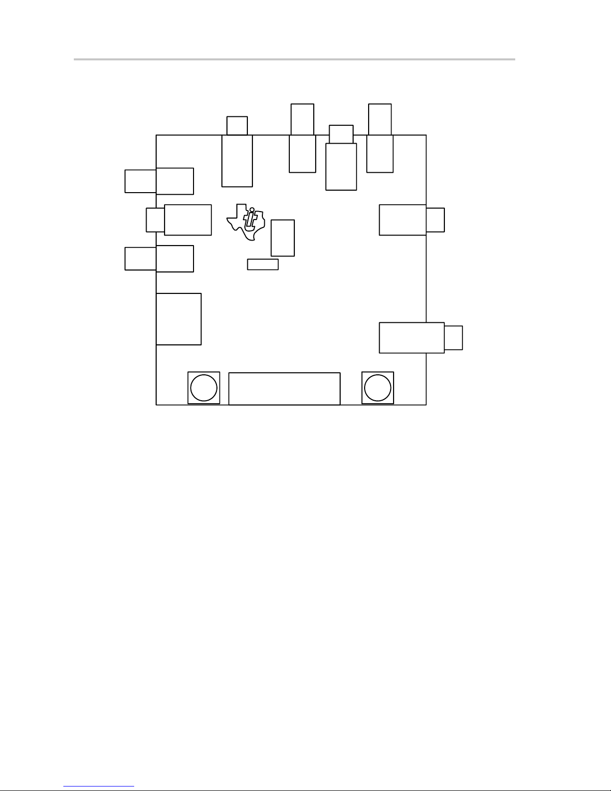
Figure 3–1.TLV320AIC23 EVM2 Parts Location Diagram
MIc
Line Out
Left OutRight Out
Left In
Right In
Connector
Line In
Parallel
Port
2
I
J1L
J3
J1
U1
J1R
C
J5
Master CLKIN
Y1
J2R J2L
J2
Headphone
J4
PJ1
Power
J7
Master CLKOUTDigital I/O
3-2
Page 15
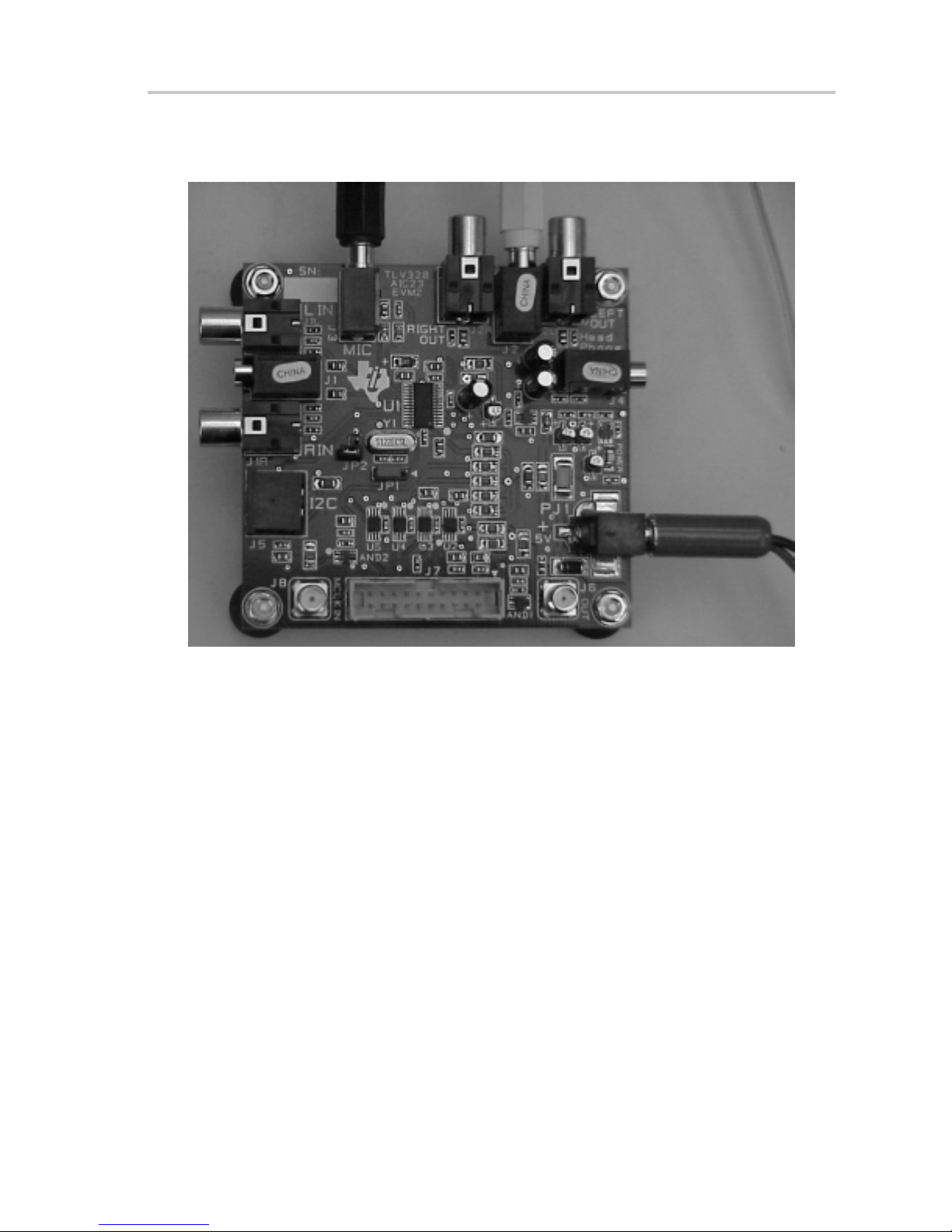
3.1 Photographs of EVM
Figure 3–2.TLV320AIC23 EVM2 Top View
Photographs of EVM
Theory of Operation
3-3
Page 16

Photographs of EVM
Figure 3–3.TLV320AIC23 EVM2 Bottom View
3-4
Page 17

Figure 3–4.Parallel Port Interface Board Top View
Photographs of EVM
Figure 3–5.Parallel Port Interface Board Bottom View
Theory of Operation
3-5
Page 18

Jumper Settings
3.2 Jumper Settings
There are two jumpers on the EVM.
- JP1 is used to select the communication mode of the EVM. Position 1–2
sets the mode for SPI. Position 2–3 sets the mode for I
software was developed for I
needs to create the necessary code. Signals needed for SPI are available
on the EVM.
- JP2 is used to select or deselect the onboard crystal for MASTER CLOCK.
Choose one of the following jumper configurations before applying power to
the EVM:
MASTER CLOCK SOURCE JP2 Y1
Master clock from onboard crystal OUT IN
Master clock supplied externally IN OUT
3.3 TLV320AIC23 EVM2 Power
The TL V320AIC23 EVM2 is powered by an external 5-Vdc power supply (not
included) to a 2,5-mm mini power jack, PJ1. LED1 indicates when power is
applied to the board.
2
C. The GUI
2
C communication. For SPI the end-user
3.4 Analog Connections
3.4.1 Microphone
A 3,5-mm mono jack is available for the microphone input, J3.
3.4.2 LINE IN Connections
A 1.0-V rms (max) input is available at the LINE IN jacks. T wo connection types
are available.
- Independent left/right RCA jacks, J1L and J1R.
- 3,5-mm stereo mini jack, J1.
3.4.3 Headphones
A headphone connection is available at J4 for 16- or 32-Ω loads. J4 is a
3,5-mm stereo mini jack.
3.4.4 LINE OUT Connectors
A 1.0-V rms (max) output is available at the LINE OUT jacks. Two connection
types are available.
- Independent left/right RCA jacks, J2L and J2R.
- 3,5-mm stereo mini jack, J2.
3-6
Page 19

3.5 Digital I/O
Digital I/O
A protected header, J7, is available for interfacing with external digital I/O. T wo
power sources, 5 V and 3.3 V, are available on J7 for powering external
boards. The 5-V power is tapped directly off PJ1. The 3.3-V power can supply
up to 100 mA.
Signal J7
5v_DIO (5.0 VDC) 1, 2
VCC_DIO (3.0 VDC) 5, 6
DIN 9
DOUT 11
BCLK 13
LRCIN 15
LRCOUT 17
MCLK 19
DIGITAL GROUND 3, 4, 7, 8, 10, 12, 14, 16, 18, 20
3.6 TLV320AIC23 EVM2 Features
3.6.1 Master Clock
The master clock can be either external or internal. For internal mode, a crystal
socket is available. For external mode, the master clock is applied to SMA jack
J8. The master clock input is 5-V tolerant. The master clock output is available
at SMA jack J6. The master clock is derived from the CLKOUT pin (U1 pin 2).
This signal has a 5-V swing.
3.6.2 Digital Loopback
Digital loopback can be enabled using the GUI. This loops DOUT to DIN via
a MUX.
3.6.3 Software Interface Connection
A PC provides control of the TLV320AIC23 EVM2 via a software GUI called
Rhino. A parallel port interface board, DAREF106, connects to the PC parallel
port. A cable with miniDIN 8-pin connectors, included in the TLV320AIC23
EVM2 kit, connects the parallel port interface board to the EVM.
Theory of Operation
3-7
Page 20

3-8
Page 21

Chapter 4
Software
This section describes the use of the DASCCT_AIC23 software GUI interface
to control the TLV320AIC23 EVM2 board. Pictures of the various interface
panels are shown, and explanations of the control and display elements on
each are provided.
Topic Page
4.1 DASCCT_AIC23 Installation 4-2. . . . . . . . . . . . . . . . . . . . . . . . . . . . . . . . . . . .
4.2 DASCCT_AIC23 Start-Up 4-4. . . . . . . . . . . . . . . . . . . . . . . . . . . . . . . . . . . . . .
4.3 DASCCT_AIC23 Overview 4-4. . . . . . . . . . . . . . . . . . . . . . . . . . . . . . . . . . . . .
4.4 Main Panel 4-4. . . . . . . . . . . . . . . . . . . . . . . . . . . . . . . . . . . . . . . . . . . . . . . . . . .
2
4.5 I
4.6 View Registers 4-8. . . . . . . . . . . . . . . . . . . . . . . . . . . . . . . . . . . . . . . . . . . . . . . .
C Adjust 4-7. . . . . . . . . . . . . . . . . . . . . . . . . . . . . . . . . . . . . . . . . . . . . . . . . . . .
Software
4-1
Page 22

DASCCT_AIC23 Installation
4.1 DASCCT_AIC23 Installation
Before running the DASCCT_AIC23 software, the parallel port must be
configured for enhanced parallel port (EPP). The parallel port configuration
can be changed in the system setup during system boot up. Some computers
have a bidirectional mode, which also works. (Some have PS2, which may
also work.) The connection diagram for the equipment is Figure 4–1.
1) Insert the software CD labeled DASCCT_AIC23 1.0 into the CD-ROM
drive of the PC.
2) Open the Start menu and then click Run.
3) Type D:\SETUP and press <ENTER>. If the CD-ROM drive is not D:,
substitute the appropriate drive letter. Follow the instructions presented by
the setup wizard.
4) Connect the analog input from a CD, DVD player , or any alternative analog
source to the TLV320AIC23/DAC23 EVM2.
5) Connect the TL V320AIC23/DAC23 EVM2 to the speakers or headphones
that will be used for listening.
6) Connect the parallel port interface card to the parallel port connector of the
PC.
2
7) Connect the cable provided in the kit between I
C connector J5 on the
TLV320AIC23/DAC23 EVM2 and connector J2 on the parallel port
interface card.
4-2
Page 23

Figure 4–1.AIC23/DAC23 EVM2 Connection Diagram
DASCCT_AIC23 Installation
PC
Analog In
CD Player
Audio Out
Speakers
I2C Connector
AIC23/DAC23 EVM
Parallel
Port
Interface
Board
Parallel
Port
Software
4-3
Page 24

DASCCT_AIC23 Start-Up
4.2 DASCCT_AIC23 Start-Up
1) Execute the software file named DASCCT_AIC23.exe from the directory
where the software was loaded.
2) Click the Master or Slave radio button to select the operating mode.
3) Click the AIC 23 or DAC 23 radio button to select the device.
4.3 DASCCT_AIC23 Overview
The EQ GUI was designed with a screen resolution of 1 152 by 864. Therefore,
the windows optimally fit on the screen using this resolution. For a screen
resolution of 800 by 600, the main window initializes higher up, toward the
center of the screen. All other resolutions initialize at the same coordinates as
designed in the 1152 by 864 screen resolution.
4.4 Main Panel
The GUI main panel is shown in Figure 4–2. The following paragraphs
describe the features seen on the main panel.
Figure 4–2.Main Panel
4.4.1 About Button
The About button is hidden under the TI logo in the upper left corner of the main
panel. Pressing this button causes a standard About box to appear with
release information about DASCCT_AIC23.
4.4.2 AIC 23 and DAC 23 Radio Buttons
These radio button allow selection of the device to be emulated by the
TLV320AIC23 EVM2, the codec or the DAC.
4.4.3 Master and Slave Radio Buttons
These radio buttons select the operating mode of the device.
4-4
Page 25

4.4.4 Message Area
Directly below the Master and Slave radio buttons on the left side of the main
panel is a message area. Short text instructions to the operator, status
indications, or error messages can appear in this box. A listing of possible error
messages appears in Chapter 5, along with an explanation of the errors.
4.4.5 Line Input Volume
The line input volume section of the main panel consists of two identical boxes,
one each for the left and right input channels. Each box contains the following:
- A level bar that indicates the volume level. To set the volume, click at the
- A Mute check box to silence the channel
- A Gang check box to tie the volume controls of both channels together.
- A display area with a numeric readout of the actual gain level setting in dB
Left and right line input volume settings can also be changed in the L Vol (Line
Input) and R Vol (Line Input) registers on the register panel (see Section 4.6.2
and Section 4.6.3, respectively).
Main Panel
desired location; the length of the bar adjusts to that point, changing the
volume level accordingly.
The channel that has its Gang box checked automatically locks the
opposite channel into a volume setting the same as its own.
4.4.6 HeadPhone Volume
The headphone volume section of the main panel consists of two identical
boxes, one each for the left and right audio channels. Each box contains the
following:
- A level bar that indicates the volume level. To set the volume, click at the
desired location; the length of the bar adjusts to that point, changing the
volume level accordingly.
- A Zero Cross check box. When the zero-cross detect circuit for the
headphone is enabled, the volume control values are only updated when
the input signal to the gain stage is close to the analog ground level.
- A Gang check box to tie the volume controls of both channels together.
The channel that has its Gang box checked automatically locks the opposite channel into a volume setting the same as its own.
- A display area with a numeric readout of the actual gain level setting in dB
Left and right headphone volume settings can also be changed in the L Vol
(HeadPhone) and R Vol (HeadPhone) registers on the register panel (see
Section 4.6.4 and Section 4.6.5, respectively).
4.4.7 RESET Button
The RESET button sends an I2C reset command to the AIC23/DAC23.
4.4.8 EXIT Button
EXIT closes all files. The EXIT button can be clicked at any time.
Software
4-5
Page 26

Main Panel
4.4.9 I2C Adjust Button
Pressing this button opens a panel that allows adjustment of the timing period
used for I2C communications between the PC and the EVM. See Section 4.5.
4.4.10 I2C Bypass Check Box
This check box allows the user to run the software without a device connected
to the parallel port.
4.4.11 DataLog On Check Box
This check box allows the user to record the information sent over I2C. The
data is always stored in a file called DataLog.txt. The { within the file represents
2
a valid I
command.
C start command. The } within the file represents a valid I2C stop
4.4.12 View Registers Button
When the View Registers button is clicked, the GUI opens a second panel.
This panel shows all the TLV320AIC23/DAC23 EVM2 registers. A function
name is displayed for each bit in each register, and the values of the bits can
be viewed or changed. A complete description including all the registers and
other functionality of the second panel is in Section 4.6.
4.4.13 Dig Loopback Check Box
Checking this box connects DOUT to DIN via a multiplexer.
4.4.14 Digital Control Button
Clicking the Digital Control button opens a panel that allows setting of the
digital audio controls (see Section 4.6.8). The digital audio controls can also
be set by putting values directly into the Audio (Digital) register on the
Registers panel (see Section 4.6).
4.4.15 Analog Control Button
Clicking the Analog Control button opens a panel that allows setting of the
analog audio controls (see Section 4.6.7). The analog audio controls can also
be set by putting values directly into the Audio (Analog) register on the
Registers panel (see Section 4.6).
4.4.16 Format Control Button
Clicking the Format Control button opens a panel that allows setting of the
audio format controls (see Section 4.6.10). The audio format controls can also
be set by putting values directly into the Audio (Format) register on the
Registers panel (see Section 4.6).
4.4.17 Normal Mode and USB Mode Radio Buttons
For information on the proper setting of normal or USB mode, see the
TLV320AIC23 data manual.
4-6
Page 27

4.4.18 Clock Select Button
Clicking the Clock Select button opens a panel that allows selection of master
clock speed and ADC and DAC sampling rates (see Section 4.6.1 1). (Do clock
selections correspond to sampling rate register bits?)
4.4.19 Frequency Display Areas
In the lower right corner of the main panel are two frequency displays. The one
on the left shows the master clock frequency MCLK in megaHertz; the one on
the right shows the DAC sampling frequency in kiloHertz.
4.5 I2C Adjust
The I2C commands are generated on the parallel port using a method referred
to as bit-banging. Because Windows does not have readily accessible timers
down into the microseconds, the I
create the delay . The number of executions of the for-loop is calibrated initially
when the program is started. This initial calibration sets SCL to 100 kHz. The
looping variable in the for-loop can be changed using the SCL period A and
" buttons, which only become active after clicking the Fine Adjust button.
To see the result of changing this variable, requires capturing the SCL output
on a storage oscilloscope. The program recalibrates SCL to 100 kHz if the
RECALIBRATE button is pressed.
I2C Adjust
2
C clocks are done using C++ for-loops to
Figure 4–3.I2C Adjust
Software
4-7
Page 28

I2C Adjust
4.6 View Registers
The registers panel, shown in Figure 4–4, displays the bits for 10 registers,
where the user can either view or change the bit values. There is a Preset
Modes section of the panel, which allows the user to call up any of three sets
of default register settings. A section with OK, Apply, and Cancel buttons
completes the registers panel. The various functions are discussed
individually in the following sections.
Figure 4–4.Register GUI
4.6.1 Preset Modes
The Preset Modes section of the panel contains a READ radio button that is
currently inactive. Functionality will be assigned to the button in a future
software release. There are also three buttons labelled Mode One, Mode Two,
and Mode Three. Each button corresponds with an ASCII text file containing
preset register values. When a button is clicked, the values in the
corresponding file are loaded into the DASCCT_AIC23 registers.
The three standard files that come with the software are shown in Figure 4–5.
The files can be edited, but must be kept in the same directory where the
DASCCT_AIC23.exe file is stored. The first column in the file is the decimal
value of the register number and the second column is the register value,
followed by an explanatory comment.
4-8
Page 29

Figure 4–5.Mode Files
I2C Adjust
Software
4-9
Page 30

L Vol (HeadPhone) Register
4.6.2 L Vol (Line Input) Register
Address: 0000000
D4–D0 set the left line input volume. D8 sets simultaneous right/left
volume/mute.
D7 sets the left input mute.
Setting the bit values in this register is functionally equivalent to operating the
Line Input Volume Left controls on the main panel (see Section 4.4.5).
4.6.3 R Vol (Line Input) Register
Address: 0000001
D4–D0 set the right line input volume. D8 sets simultaneous right/left
volume/mute.
D7 sets the right input mute.
Setting the bit values in this register is functionally equivalent to operating the
Line Input Volume Right controls on the main panel (see Section 4.4.5).
4.6.4 L Vol (HeadPhone) Register
Address: 0000010
D6–D0 set the volume control for the left headphone. D7 enables the
zero-cross detect. D8 sets simultaneous right/left volume/mute.
Setting the bit values in this register is functionally equivalent to operating the
HeadPhone Volume Left controls on the main panel (see Section 4.4.6).
4.6.5 R Vol (HeadPhone) Register
Address: 0000011
D6–D0 set the volume control for the right headphone. D7 enables the
zero-cross detect. D8 sets simultaneous right/left volume/mute.
Setting the bit values in this register is functionally equivalent to operating the
HeadPhone Volume Right controls on the main panel (see Section 4.4.6).
4.6.6 OK, Apply, and Cancel Buttons
The Cancel button undoes any changes that have been made in register bit
values, so the register panel matches the current state of the EVM registers.
The Apply button sends the current bit values shown on the register panel to
the EVM and stores them in the EVM registers. The OK button performs the
same function as the Apply button and simultaneously closes the register
panel.
4.6.7 Audio (Analog) Register
Address: 0000100
4-10
Page 31

D7–D6 set the sidetone attenuation (00 = –6 dB, 01 = –9 dB, 10 = –12 dB,
11 = –15 dB). D5 sets sidetone enable (0 = disabled, 1 = enabled). D4 sets the
DAC select (0 = DAC off, 1 = DAC selected). D3 sets the bypass (0 = disabled,
1 = enabled). D2 sets the input for the ADC (0 = line, 1 = microphone). D1 sets
the microphone mute (0 = normal, 1 = muted). D0 sets the microphone boost
(0 = 0 db, 1 = 20 dB).
Clicking the Analog Control button opens an Analog Control panel (see
Figure 4–6) that allows setting all the analog audio parameters without
reference to their bit values. The Analog Control button in the analog audio
register box is functionally identical to the Analog Control button on the main
panel (see Section 4.4.15).
The Cancel button undoes any changes that have been made in register bit
values, so the register panel matches the current state of the EVM registers.
The Apply button sends the current bit values shown on the Analog Control
panel to the Audio (Analog) register section of the register panel. The OK
button performs the same function as the Apply button and simultaneously
closes the register panel.
Figure 4–6.Analog Control
Audio (Digital) Register
4.6.8 Audio (Digital) Register
Address: 0000101
D3 sets the DAC soft mute (0 = disabled, 1 = enabled). D2–D1 set the
de-emphasis control (00 = disabled, 01 = 32 kHz, 10 = 44.1 kHz, 1 1 = 48 kHz).
D0 sets the ADC high-pass filter (0 = disabled, 1 = enabled).
Clicking the Digital Control button opens a Digital Control panel (see
Figure 4–7) that allows setting all the digital audio parameters without
reference to their bit values. The Digital Control button in the digital audio
register box is functionally identical to the Digital Control button on the main
panel (see Section 4.4.14).
The Cancel button undoes any changes that have been made in register bit
values, so the register panel matches the current state of the EVM registers.
Software
4-11
Page 32

Power Down Register
The Apply button sends the current bit values shown on the Analog Control
panel to the Audio (Digital) register section of the register panel. The OK button
performs the same function as the Apply button and simultaneously closes the
register panel.
Figure 4–7.Digital Control
4.6.9 Power Down Register
Address: 0000110
D7 sets the device power. D6 sets CLK. D5 sets the oscillator. D4 sets the
outputs. D3 sets the DAC. D2 sets the ADC. D1 sets the microphone input. D0
sets the line input.
Clicking the Send Data button sends only the power down data without clicking
the Apply button.
4.6.10 Audio (Format) Register
Address: 0000111
D6 sets master/slave (0 = slave, 1 = master). D5 sets the DAC left/right swap
(0 = disabled, 1 = enabled). D4 sets the DAC left/right phase (0 = right channel
on, LRCIN high, 1 = LRCIN low). In DSP mode (0 = MSB is available on the
first BCLK rising edge after an LRCIN rising edge, 1 = MSB is available on the
second BCLK rising edge after an LRCIN rising edge). D3–D2 set the input
word length (00 = 16b, 01 = 20b, 10 = 24b, 1 1 = 32b). D1–D0 set the data format
(1 1 = DSP; 10 = I
Clicking the Format Control button opens a Format Control panel (see
Figure 4–8) that allows setting all the audio format parameters without
reference to their bit values. The Format Control button in the audio format
register box is functionally identical to the Format Control button on the main
panel (see Section 4.4.16).
2
S; 01 = MSB first, left aligned; 00 = MSB first, right aligned).
The Cancel button undoes any changes that have been made in register bit
values, so the register panel matches the current state of the EVM registers.
4-12
Page 33

The Apply button sends the current bit values shown on the Analog Control
panel to the Audio (Format) register section of the register panel. The OK
button performs the same function as the Apply button and simultaneously
closes the register panel.
Figure 4–8.Format Control
4.6.11 Sampling Rate Register
Sampling Rate Register
Address: 0001000
D7 sets the clock output divider (0 = MCLK, 1 = MCLK/2), D6 sets clock input
divider (0 = MCLK, 1 = MCLK/2). D5–D2 set the SR3–SR0 bits. D1 sets the
base oversampling rate (In USB mode, 0 = 250 f
mode, 0 = 256 f
1 = 384 fS). D0 sets the USB/normal mode (0 = normal,
S and
1 = 272 fS; in normal
S and
1 = USB).
Clicking the Clock Select button opens a Normal Clock Setup panel (see
Figure 4–9) that allows the selection of master clock speed and ADC and DAC
sampling rates. There are also two check boxes for setting the clock input
divider and clock output divider on or off. Because the correspondence
between clock settings and register bit values is not intuitively obvious, it may
be easier to input the desired clock frequency and sampling rates in the Normal
Clock Setup panel and observe the bit settings that appear in the registers
panel. The Clock Select button in the sampling rate register box is functionally
identical to the Clock Select button on the main panel (see Section 4.4.18).
The Cancel button undoes any changes that have been made in register bit
values, so the register panel matches the current state of the EVM registers.
The Apply button sends the current bit values shown on the Analog Control
panel to the Sampling Rate register section of the register panel. The OK
button performs the same function as the Apply button and simultaneously
closes the register panel.
Software
4-13
Page 34

Interface Activate Register
Figure 4–9.Clock Setup
4.6.12 Interface Activate Register
Address: 0001001
D0 activates the digital interface (0 = inactive, 1 = active).
Clicking the Send Data button sends only the interface activation data without
clicking the Apply button.
4-14
Page 35

The error messages are only visible during error conditions. The error
messages are located just above the RESET button in the main panel. The first
message to appear will be above the second message. For example, if an ACK
error occurs first then it is displayed first and it is only displayed once. The
software continues to send data to the device even with ACK and WAIT errors.
But it no longer looks for ACK or WAIT errors, therefore the response from the
device can be undetermined.
No. Error Message Cause
Chapter 5
I2C Error Messages
1 ACK error
2 WAIT error
The AIC23/DAC23 is not sending an acknowledge command back to the host processor.
This is referred to as an ACK in I
transactions.
Pin 1 (SDA) or pin 14 (SCL) on the parallel cable is not allowing the I2C commands to
reach the EVM.
Pin 15 on the parallel cable is not allowing the ACK command to return back to the host.
The LPT port is not connected and configured for EPP or bidirectional mode (PS-2 in
some cases).
The actual LPT port connected does not match the LPT port selected in the *.dat file.
LPT1 is the default for the LPT port, if it is not explicitly defined in the file. The
hexadecimal addresses for the ports defined in the software are LPT1 = 0x378,
LPT2 = 0x278, and LPT3 = 0x3BC.
The actual LPT port base address selected does not match any of the following
hexadecimal addresses:
LPT1 = 0x378
LPT2 = 0x278
LPT3 = 0x3BC
The AIC23/DAC23 is holding the SCL line low and not releasing it for the host processor.
This is referred to as waiting the bus in I
does not terminate the transactions.
Pin 1 (SDA) or pin 14 (SCL) on the parallel cable is not allowing the I2C commands to
reach the EVM.
Pin 10 on the parallel cable is not allowing the host to read a high SCL. Therefore a WAIT
is assumed.
2
C terminology. The software does not terminate the
2
C terminology. The AIC23/DAC23 software
I2C Error Messages
5-1
Page 36

5-2
Page 37

Chapter 6
Kit Contents
This chapter contains a list of the contents of the TL V320AIC23 EVM2 kit and
a bill of materials for the TLV320AIC23 EVM2 board.
Topic Page
6.1 TLV320AIC23 EVM2 Kit Contents 6-2. . . . . . . . . . . . . . . . . . . . . . . . . . . . . . .
6.2 Bill of Materials 6-3. . . . . . . . . . . . . . . . . . . . . . . . . . . . . . . . . . . . . . . . . . . . . . .
Kit Contents
6-1
Page 38

TLV320AIC23 EVM2 Kit Contents
6.1 TLV320AIC23 EVM2 Kit Contents
TLV320AIC23 EVM2 is shipped with the following:
1) TLV320AIC23 EVM2 evaluation module
2) DAREF106R2 parallel port interface board
3) TLV320AIC23 EVM2 CD. The CD contains the following:
a) TLV320AIC23 data manual
b) TLV320AIC23 EVM2 user’s guide
c) Schematic
d) Bill of materials
e) PCB
f) Gerbers
g) GUI software
4) Parallel port cable, 8-pin
6-2
Page 39

Bill of Materials
6.2 Bill of Materials
Description Qty. Part Number Mfr. Ref. Des.
AND Gate, Single 2–Input Positive 1 SN74AHC1G08DBVR Texas Instruments AND2
AND Gate, Single 2–Input Positive 1 SN74AHCT1G08DBVR Texas Instruments AND1
Buffer/Driver , Dual w/3–State Outputs 3 SN74LVC2G241DCTR Texas Instruments U3, U4, U5
CAP 27PFD 50V CERM 0603 NPO 2 ECU–V1H270JCV Panasonic C13, C14
CAP 47PFD 50V CERM 0603 NPO 3 ECJ–1VC1H470J Panasonic C3, C5, C8
CAP .01UFD 16V CERM 0603 X7R 2 ECJ–1VB1C104K Panasonic C15, C25
CAP .01UFD 25V CERM 0603 X7R 11 ECJ–1VB1E103K Panasonic C21, C23, C29, C31,
C33, C35, C36, C38,
C40, C42, C43
CAP 0.1UFD 50V CERM 0805 X7R 1 ECJ–2YB1H104K Panasonic C12
CAP 1.0UFD 16V CERM 0805 X7R 14 ECJ–2VF1C105Z Panasonic C1, C2, C4, C6, C7, C20,
C22, C28, C30, C32,
C34, C37, C39, C41
CAP 10UFD 6.3V TANT ELEC SMD TEA 1 ECS–T0JY106R Panasonic C11
CAP 10UFD 16V ALUM ELEC SM–VSA 4 ECE–V1CS100SR Panasonic C16, C17, C18, C19
CAP 100UFD 10V RAD ALUM ELEC
HFQ
Codec, 16–Bit Stereo Audio 1 TLV320AIC23PW Texas Instruments U1
Connector, 20 Pin Box Header 1 2520–6002UB 3M J7
Ferrite Bead, 11 Ohms 1.5A SM0805 2 MI0805K110R–00 Steward FB5, FB7
Ferrite Bead, 31 Ohms 1.5A SM1206 3 MI1206K310R–00 Steward FB1, FB3, FB4
Header, 2 Pin Male, Straight, Gold 1 PZC02SAAN Sullins JP2
Header, 3 Pin Male, Straight, Gold 1 PZC03SAAN Sullins JP1
Jack, MINI–Mono, PCB–RA, 3,5 mm 1 MJ–3502N CUI Stack J3
Jack, MINI–Stereo, PCB–RA, 3,5 mm 3 SJ–3535N CUI Stack J4, J1, J2
Jack, PWR–MINI, 2.5mm SMD+TH 1 RASH712 Switchcraft PJ1
Jack, RCA, PCB–Right Angle, Black 4 16PJ097 DGS Pro Audio J1L, J1R, J2L, J2R
Jack, SMA PCB Gold 2 901–144–8–RFX Amphenol J8, J6
Jack, PS2–Female, 8 Position, PCB–
Right Angle
LED, Red SM1206 1 CMD15–21VRD/TR8 Chicago Miniature LED1
3 ECA–1AFQ101 Panasonic C9, C10, C24
1 MD–80S CUI Stack J5
MUX, Single 2to1 W/Common Strobe 1 SN74LVC2G157DCTR Texas Instruments U2
Rectifier, Silicon 1A 400V 1 DL400413 Diodes, Inc. CR2
Rectifier, SW 0.15A 75V SMT MiniMELF 1 DL4148 Micro Commercial
RES 0.0 OHM 1/10W 5% SMD 0805 1 ERJ–GEY0R00V Panasonic R7
Co.
CR1
Kit Contents
6-3
Page 40

Bill of Materials
Description Ref. Des.Mfr.Part NumberQty.
RES 3.3 OHM 1/8W 5% SMD 1206 9 ERJ–8RQJ3R3V Panasonic R11, R12, R13, R14,
R15, R16, R19, R27, R29
RES 10.0 OHM 1/8W 1% SMD 1206 1 ERJ–8ENF10R0V Panasonic R17
RES 10 OHM 1W 5% SMD 2512 1 ERJ–1WY100U Panasonic R18
RES 49.9 OHM 1/16W 1% SMD 0603 1 ERJ–3EKF49R9V Panasonic R31
RES 49.9 OHM 1/8W 1% SMD 1206 1 ERJ–8ENF49R9V Panasonic R33
RES 499 OHM 1/16W 1% SMD 0603 1 ERJ–3EKF4990V Panasonic R26
RES 2.2K OHM 1/10W 5% SMD 0805 1 ERJ–6GEYJ222V Panasonic R8
RES 4.99K OHM 1/16W 1% SMD 0603 6 ERJ–3EKF4991V Panasonic R1, R2, R4, R5, R30, R32
RES 100K OHM 1/16W 1% SMD 0603 5 ERJ–3EKF1003V Panasonic R3, R6, R9, R10, R22
RES 169K OHM 1/16W 1% SMD 0603 2 ERJ–3EKF1693V Panasonic R24, R25
RES 301K OHM 1/16W 1% SMD 0603 2 ERJ–3EKF3013V Panasonic R21, R23
Voltage regulator , LDO–Adj., 150mA 2 TPS76301DBVR Texas Instruments VR1, VR2
6-4
Page 41

Appendix A
Appendix A
Circuit Card and Schematic
This appendix contains the following items for the TL V320AIC23 EVM2, in the
order listed:
1) Top silkscreen
2) Copper layer 1
3) Copper layer 2
4) Schematic diagram
Page 42

Thu Nov 29 10:48:53 2001
Page 43

Thu Nov 29 10:46:27 2001
Page 44

Thu Nov 29 10:47:13 2001
Page 45

Page 46

Page 47

 Loading...