


l
!"# #$! %$&'
Data M anua
February 2004 Digital Audio Products
SLWS106H

Contents
Section Title Page
1 Introduction 1−1. . . . . . . . . . . . . . . . . . . . . . . . . . . . . . . . . . . . . . . . . . . . . . . . . . . . . .
1.1 Features 1−1. . . . . . . . . . . . . . . . . . . . . . . . . . . . . . . . . . . . . . . . . . . . . . . . . . .
1.2 Functional Block Diagram 1−3. . . . . . . . . . . . . . . . . . . . . . . . . . . . . . . . . . . .
1.3 Terminal Assignments 1−4. . . . . . . . . . . . . . . . . . . . . . . . . . . . . . . . . . . . . . . .
1.4 Ordering Information 1−5. . . . . . . . . . . . . . . . . . . . . . . . . . . . . . . . . . . . . . . . .
1.5 Terminal Functions 1−5. . . . . . . . . . . . . . . . . . . . . . . . . . . . . . . . . . . . . . . . . .
2 Specifications 2−1. . . . . . . . . . . . . . . . . . . . . . . . . . . . . . . . . . . . . . . . . . . . . . . . . . . .
2.1 Absolute Maximum Ratings Over Operating Free-Air Temperature
Range 2−1. . . . . . . . . . . . . . . . . . . . . . . . . . . . . . . . . . . . . . . . . . . . . . . . . . . . .
2.2 Recommended Operating Conditions 2−1. . . . . . . . . . . . . . . . . . . . . . . . . .
2.3 Electrical Characteristics Over Recommended Operating
Conditions 2−2. . . . . . . . . . . . . . . . . . . . . . . . . . . . . . . . . . . . . . . . . . . . . . . . . .
2.3.1 ADC 2−2. . . . . . . . . . . . . . . . . . . . . . . . . . . . . . . . . . . . . . . . . . . . . .
2.3.2 DAC 2−3. . . . . . . . . . . . . . . . . . . . . . . . . . . . . . . . . . . . . . . . . . . . . .
2.3.3 Analog Line Input to Line Output (Bypass) 2−3. . . . . . . . . . . . .
2.3.4 Stereo Headphone Output 2−4. . . . . . . . . . . . . . . . . . . . . . . . . . .
2.3.5 Analog Reference Levels 2−4. . . . . . . . . . . . . . . . . . . . . . . . . . . .
2.3.6 Digital I/O 2−4. . . . . . . . . . . . . . . . . . . . . . . . . . . . . . . . . . . . . . . . . .
2.3.7 Supply Current 2−4. . . . . . . . . . . . . . . . . . . . . . . . . . . . . . . . . . . . .
2.4 Digital-Interface Timing 2−5. . . . . . . . . . . . . . . . . . . . . . . . . . . . . . . . . . . . . . .
2.4.1 Audio Interface (Master Mode) 2−5. . . . . . . . . . . . . . . . . . . . . . .
2.4.2 Audio Interface (Slave-Mode) 2−6. . . . . . . . . . . . . . . . . . . . . . . .
2.4.3 Three-Wire Control Interface (SDIN) 2−7. . . . . . . . . . . . . . . . . .
2.4.4 Two-Wire Control Interface 2−7. . . . . . . . . . . . . . . . . . . . . . . . . . .
3 How to Use the TLV320AIC23B 3−1. . . . . . . . . . . . . . . . . . . . . . . . . . . . . . . . . . . . .
3.1 Control Interfaces 3−1. . . . . . . . . . . . . . . . . . . . . . . . . . . . . . . . . . . . . . . . . . .
3.1.1 SPI 3−1. . . . . . . . . . . . . . . . . . . . . . . . . . . . . . . . . . . . . . . . . . . . . . .
3.1.2 2-Wire 3−1. . . . . . . . . . . . . . . . . . . . . . . . . . . . . . . . . . . . . . . . . . . . .
3.1.3 Register Map 3−2. . . . . . . . . . . . . . . . . . . . . . . . . . . . . . . . . . . . . . .
3.2 Analog Interface 3−5. . . . . . . . . . . . . . . . . . . . . . . . . . . . . . . . . . . . . . . . . . . . .
3.2.1 Line Inputs 3−5. . . . . . . . . . . . . . . . . . . . . . . . . . . . . . . . . . . . . . . . .
3.2.2 Microphone Input 3−6. . . . . . . . . . . . . . . . . . . . . . . . . . . . . . . . . . .
3.2.3 Line Outputs 3−6. . . . . . . . . . . . . . . . . . . . . . . . . . . . . . . . . . . . . . .
3.2.4 Headphone Output 3−6. . . . . . . . . . . . . . . . . . . . . . . . . . . . . . . . . .
3.2.5 Analog Bypass Mode 3−7. . . . . . . . . . . . . . . . . . . . . . . . . . . . . . . .
3.2.6 Sidetone Insertion 3−7. . . . . . . . . . . . . . . . . . . . . . . . . . . . . . . . . .
3.3 Digital Audio Interface 3−7. . . . . . . . . . . . . . . . . . . . . . . . . . . . . . . . . . . . . . . .
3.3.1 Digital Audio-Interface Modes 3−7. . . . . . . . . . . . . . . . . . . . . . . .
iii

3.3.2 Audio Sampling Rates 3−9. . . . . . . . . . . . . . . . . . . . . . . . . . . . . . .
3.3.3 Digital Filter Characteristics 3−11. . . . . . . . . . . . . . . . . . . . . . . . . .
A Mechanical Data A−1. . . . . . . . . . . . . . . . . . . . . . . . . . . . . . . . . . . . . . . . . . . . . . . . . .
iv

List of Illustrations
Figure Title Page
2−1 System-Clock Timing Requirements 2−5. . . . . . . . . . . . . . . . . . . . . . . . . . . . . . .
2−2 Master-Mode Timing Requirements 2−5. . . . . . . . . . . . . . . . . . . . . . . . . . . . . . .
2−3 Slave-Mode Timing Requirements 2−6. . . . . . . . . . . . . . . . . . . . . . . . . . . . . . . .
2−4 Three-Wire Control Interface Timing Requirements 2−7. . . . . . . . . . . . . . . . . .
2−5 Two-Wire Control Interface Timing Requirements 2−7. . . . . . . . . . . . . . . . . . .
3−1 SPI Timing 3−1. . . . . . . . . . . . . . . . . . . . . . . . . . . . . . . . . . . . . . . . . . . . . . . . . . . . .
3−2 2-Wire Compatible Timing 3−2. . . . . . . . . . . . . . . . . . . . . . . . . . . . . . . . . . . . . . .
3−3 Analog Line Input Circuit 3−5. . . . . . . . . . . . . . . . . . . . . . . . . . . . . . . . . . . . . . . . .
3−4 Microphone Input Circuit 3−6. . . . . . . . . . . . . . . . . . . . . . . . . . . . . . . . . . . . . . . . .
3−5 Right-Justified Mode Timing 3−7. . . . . . . . . . . . . . . . . . . . . . . . . . . . . . . . . . . . . .
3−6 Left-Justified Mode Timing 3−8. . . . . . . . . . . . . . . . . . . . . . . . . . . . . . . . . . . . . . .
3−7 I2S Mode Timing 3−8. . . . . . . . . . . . . . . . . . . . . . . . . . . . . . . . . . . . . . . . . . . . . . .
3−8 DSP Mode Timing 3−8. . . . . . . . . . . . . . . . . . . . . . . . . . . . . . . . . . . . . . . . . . . . . .
3−9 Digital De-Emphasis Filter Response − 44.1 kHz Sampling 3−12. . . . . . . . . . .
3−10 Digital De-Emphasis Filter Response − 48 kHz Sampling 3−12. . . . . . . . . . . .
3−11 ADC Digital Filter Response 0: USB Mode
(Group Delay = 12 Output Samples) 3−13. . . . . . . . . . . . . . . . . . . . . . . . . . . . . .
3−12 ADC Digital Filter Ripple 0: USB
(Group Delay = 20 Output Samples) 3−13. . . . . . . . . . . . . . . . . . . . . . . . . . . . . .
3−13 ADC Digital Filter Response 1: USB Mode Only 3−14. . . . . . . . . . . . . . . . . . . .
3−14 ADC Digital Filter Ripple 1: USB Mode Only 3−14. . . . . . . . . . . . . . . . . . . . . . . .
3−15 ADC Digital Filter Response 2: USB mode and Normal Modes
(Group Delay = 3 Output Samples) 3−15. . . . . . . . . . . . . . . . . . . . . . . . . . . . . . . .
3−16 ADC Digital Filter Ripple 2: USB Mode and Normal Modes 3−15. . . . . . . . . . .
3−17 ADC Digital Filter Response 3: USB Mode Only 3−16. . . . . . . . . . . . . . . . . . . .
3−18 ADC Digital Filter Ripple 3: USB Mode Only 3−16. . . . . . . . . . . . . . . . . . . . . . . .
3−19 DAC Digital Filter Response 0: USB Mode 3−17. . . . . . . . . . . . . . . . . . . . . . . . .
3−20 DAC Digital Filter Ripple 0: USB Mode 3−17. . . . . . . . . . . . . . . . . . . . . . . . . . . .
3−21 DAC Digital Filter Response 1: USB Mode Only 3−18. . . . . . . . . . . . . . . . . . . .
3−22 DAC Digital Filter Ripple 1: USB Mode Only 3−18. . . . . . . . . . . . . . . . . . . . . . . .
3−23 DAC Digital Filter Response 2: USB Mode and Normal Modes 3−19. . . . . . . .
3−24 DAC Digital Filter Ripple 2: USB Mode and Normal Modes 3−19. . . . . . . . . . .
3−25 DAC Digital Filter Response 3: USB Mode Only 3−20. . . . . . . . . . . . . . . . . . . .
3−26 DAC Digital Filter Ripple 3: USB Mode Only 3−20. . . . . . . . . . . . . . . . . . . . . . . .
v

vi

1 Introduction
The TLV320AIC23B is a high-performance stereo audio codec with highly integrated analog functionality. The
analog-to-digital converters (ADCs) and digital-to-analog converters (DACs) within the TLV320AIC23B use multibit
sigma-delta technology with integrated oversampling digital interpolation filters. Data-transfer word lengths of 16, 20,
24, and 32 bits, with sample rates from 8 kHz to 96 kHz, are supported. The ADC sigma-delta modulator features
third-order multibit architecture with up to 90-dBA signal-to-noise ratio (SNR) at audio sampling rates up to 96 kHz,
enabling high-fidelity audio recording in a compact, power-saving design. The DAC sigma-delta modulator features
a second-order multibit architecture with up to 100-dBA SNR at audio sampling rates up to 96 kHz, enabling
high-quality digital audio-playback capability, while consuming less than 23 mW during playback only. The
TLV320AIC23B is the ideal analog input/output (I/O) choice for portable digital audio-player and recorder
applications, such as MP3 digital audio players.
Integrated analog features consist of stereo-line inputs with an analog bypass path, a stereo headphone amplifier,
with analog volume control and mute, and a complete electret-microphone-capsule biasing and buffering solution.
The headphone amplifier is capable of delivering 30 mW per channel into 32 Ω. The analog bypass path allows use
of the stereo-line inputs and the headphone amplifier with analog volume control, while completely bypassing the
codec, thus enabling further design flexibility, such as integrated FM tuners. A microphone bias-voltage output
provides a low-noise current source for electret-capsule biasing. The AIC23B has an integrated adjustable
microphone amplifier (gain adjustable from 1 to 5) and a programmable gain microphone amplifier (0 dB or 20 dB).
The microphone signal can be mixed with the output signals if a sidetone is required.
While the TLV320AIC23B supports the industry-standard oversampling rates of 256 f
oversampling rates of 250 f
and 272 fs are provided, which optimize interface considerations in designs using TI C54x
s
digital signal processors (DSPs) and universal serial bus (USB) data interfaces. A single 12-MHz crystal can supply
clocking to the DSP, USB, and codec. The TLV320AIC23B features an internal oscillator that, when connected to a
12-MHz external crystal, provides a system clock to the DSP and other peripherals at either 12 MHz or 6 MHz, using
an internal clock buffer and selectable divider. Audio sample rates of 48 kHz and compact-disc (CD) standard 44.1
kHz are supported directly from a 12-MHz master clock with 250 f
and 272 fs oversampling rates.
s
Low power consumption and flexible power management allow selective shutdown of codec functions, thus
extending battery life in portable applications. This design solution, coupled with the industry’s smallest package, the
TI proprietary MicroStar Junior using only 25 mm
2
of board area, makes powerful portable stereo audio designs
easily realizable in a cost-effective, space-saving total analog I/O solution: the TLV320AIC23B.
and 384 fs, unique
s
1.1 Features
• High-Performance Stereo Codec
− 90-dB SNR Multibit Sigma-Delta ADC (A-weighted at 48 kHz)
− 100-dB SNR Multibit Sigma-Delta DAC (A-weighted at 48 kHz)
− 1.42 V – 3.6 V Core Digital Supply: Compatible With TI C54x DSP Core Voltages
− 2.7 V – 3.6 V Buffer and Analog Supply: Compatible Both TI C54x DSP Buffer Voltages
− 8-kHz – 96-kHz Sampling-Frequency Support
• Software Control Via TI McBSP-Compatible Multiprotocol Serial Port
− 2-wire-Compatible and SPI-Compatible Serial-Port Protocols
− Glueless Interface to TI McBSPs
• Audio-Data Input/Output Via TI McBSP-Compatible Programmable Audio Interface
2
S-Compatible Interface Requiring Only One McBSP for both ADC and DAC
−I
− Standard I
− 16/20/24/32-Bit Word Lengths
MicroStar Junior is a trademark of Texas Instruments.
2
S, MSB, or LSB Justified-Data Transfers
1−1

− Audio Master/Slave Timing Capability Optimized for TI DSPs (250/272 fs), USB mode
− Industry-Standard Master/Slave Support Provided Also (256/384 f
), Normal mode
s
− Glueless Interface to TI McBSPs
• Integrated Total Electret-Microphone Biasing and Buffering Solution
− Low-Noise MICBIAS pin at 3/4 AVDD for Biasing of Electret Capsules
− Integrated Buffer Amplifier With Tunable Fixed Gain of 1 to 5
− Additional Control-Register Selectable Buffer Gain of 0 dB or 20 dB
• Stereo-Line Inputs
− Integrated Programmable Gain Amplifier
− Analog Bypass Path of Codec
• ADC Multiplexed Input for Stereo-Line Inputs and Microphone
• Stereo-Line Outputs
− Analog Stereo Mixer for DAC and Analog Bypass Path
• Volume Control With Mute on Input and Output
• Highly Efficient Linear Headphone Amplifier
− 30 mW into 32 Ω From a 3.3-V Analog Supply Voltage
• Flexible Power Management Under Total Software Control
− 23-mW Power Consumption During Playback Mode
− Standby Power Consumption <150 µW
− Power-Down Power Consumption <15 µW
• Industry’s Smallest Package: 32-Pin TI Proprietary MicroStar Junior
2
Total Board Area
−25 mm
− 28-Pin TSSOP Also Is Available (62 mm
2
Total Board Area)
• Ideally Suitable for Portable Solid-State Audio Players and Recorders
1−2
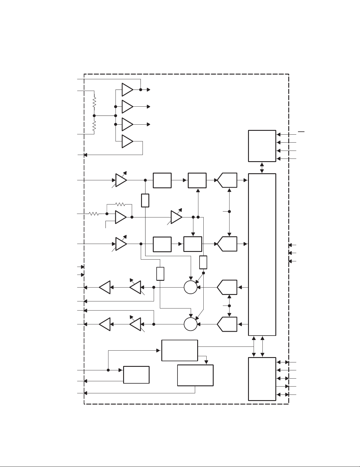
1.2 Functional Block Diagram
VMID
AVDD
AGND
MICBIAS
RLINEIN
MICIN
LLINEIN
HPVDD
HPGND
RHPOUT
50 kΩ
50 kΩ
12 to −34.5 dB,
10 kΩ
VMID
12 to −34 dB,
Headphone
Driver
1.0X
1.0X
1.0X
1.5X
1.5 dB Steps
50 kΩ
1.5 dB Steps
6 to −73 dB,
1 dB Steps
VMID
VDAC
VADC
Line
Mute
Bypass
Mute
Line
Mute
Mute,
0 dB, 20 dB
Bypass
Mute
DSPcodec
TLV320AIC23B
2:1
MUX
VADC
2:1
MUX
Side Tone
Mute
Σ
Σ−∆
ADC
Σ−∆
ADC
Σ−∆
DAC
Control
Interface
Digital
Filters
CS
SDIN
SCLK
MODE
DVDD
BVDD
DGND
ROUT
LOUT
LHPOUT
Headphone
Driver
XTI/MCLK
XTO
CLKOUT
NOTE: MCLK, BCLK, and SCLK are all asynchronous to each other.
6 to −73 dB,
1 dB Steps
(1x, 1/2x)
OSC
Σ
CLKIN
Divider
CLKOUT
Divider
(1x, 1/2x)
VDAC
Σ−∆
DAC
Digital
Audio
Interface
LRCIN
DIN
LRCOUT
DOUT
BCLK
1−3
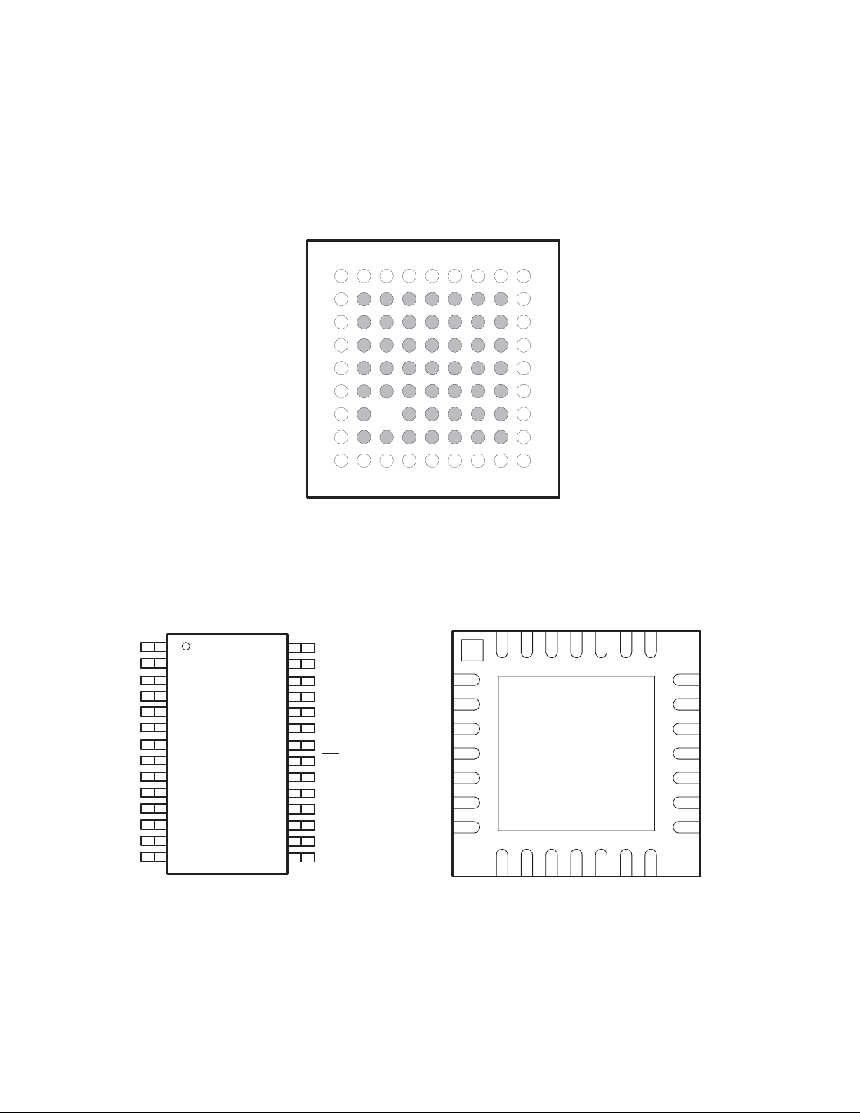
1.3 Terminal Assignments
GQE/ZQE PACKAGE
(TOP VIEW)
NC
DIN
BCLK
CLKOUT
BVDD
DGND
DVDD
XTO
25 24 23 22 21 20 19 18 17
NC
BVDD
CLKOUT
BCLK
DIN
LRCIN
DOUT
LRCOUT
HPVDD
LHPOUT
RHPOUT
HPGND
LOUT
ROUT
AVDD
PW PACKAGE
(TOP VIEW)
1
2
3
4
5
6
7
8
9
10
11
12
13
14
LRCIN
DOUT
LRCOUT
HPVDD
LHPOUT
RHPOUT
HPGND
26
27
28
29
30
31
32
123456789
NC
LOUT
NC − No internal connection
28
27
26
25
24
23
22
21
20
19
18
17
16
15
DGND
DVDD
XTO
XTI/MCLK
SCLK
SDIN
MODE
CS
LLINEIN
RLINEIN
MICIN
MICBIAS
VMID
AGND
ROUT
AVDD
DIN
LRCIN
DOUT
LROUT
HPVDD
LHPOUT
RHPOUT
VMID
AGND
MICBIAS
1
2
3
4
5
6
7
16
15
14
13
12
11
10
NC
MICIN
RHD PACKAGE
BCLK
CLKOUT
28
27
8
9
XTI/MCLK
SCLK
SDIN
MODE
CS
LLINEIN
RLINEIN
(TOP VIEW)
BVDD
DGND
26
25
11
10
DVDD
24
12
XTO
23
13
XTI/MCLK
22
21
20
19
18
17
16
15
14
SCLK
SDIN
MODE
CS
LLNEIN
RUNEIN
MICIN
1−4
LOUT
HPGND
ROUT
AVDD
AGND
VMID
MICBIAS
1.4 Ordering Information
I/O
DESCRIPTION
PACKAGE
T
A
−10°C to 70°C TLV320AIC23BGQE/ZQE TLV320AIC23BPW TLV320AIC23BRHD
−40°C to 85°C TLV320AIC23BIGQE/ZQE TLV320AIC23BIPW TLV320AIC23BIRHD
MicroStar Junior GQE/ZQE
32-Pin
28-Pin
TSSOP PW
28-Pin
PQFP RHD
1.5 Terminal Functions
TERMINAL
NO.
NAME
AGND 5 15 12 Analog supply return
AVDD 4 14 11 Analog supply input. Voltage level is 3.3 V nominal.
BCLK 23 3 28 I/O I2S serial-bit clock. In audio master mode, the AIC23B generates this signal and sends it to th e
BVDD 21 1 26 Buffer supply input. Voltage range is from 2.7 V to 3.6 V.
CLKOUT 22 2 27 O Clock output. This is a buf fered version of the XTI input and is available in 1X or 1/2X frequencies
CS 12 21 18 I Control port input latch/address select. For SPI control mode this input acts as the data latch
DIN 24 4 1 I I2S format serial data input to the sigma-delta stereo DAC
DGND 20 28 25 Digital supply return
DOUT 27 6 3 O I2S format serial data output from the sigma-delta stereo ADC
DVDD 19 27 24 Digital supply input. Voltage range is 1.4 V to 3.6 V.
HPGND 32 11 8 Analog headphone amplifier supply return
HPVDD 29 8 5 Analog headphone amplifier supply input. Voltage level is 3.3 V nominal.
LHPOUT 30 9 6 O Left stereo mixer-channel amplified headphone output. Nominal 0-dB output level is 1 V
LLINEIN 11 20 17 I Left stereo-line input channel. Nominal 0-dB input level is 1 V
LOUT 2 12 9 O Left stereo mixer-channel line output. Nominal output level is 1.0 V
LRCIN 26 5 2 I/O I2S DAC-word clock signal. In audio master mode, the AIC23B generates this framing signal
LRCOUT 28 7 4 I/O I2S ADC-word clock signal. In audio master mode, the AIC23B generates this framing signal
MICBIAS 7 17 14 O Buffered low-noise-voltage output suitable for electret-microphone-capsule biasing. Voltage
MICIN 8 18 15 I Buffered amplifier input suitable for use with electret-microphone capsules. Without external
MODE 13 22 19 I Serial-interface-mode input. See Section 3.1 for details.
NC 1, 9
RHPOUT 31 10 7 O Right stereo mixer-channel amplified headphone output. Nominal 0-dB output level is 1 V
RLINEIN 10 19 16 I Right stereo-line input channel. Nominal 0-dB input level is 1 V
ROUT 3 13 10 O Right stereo mixer-channel line output. Nominal output level is 1.0 V
GQE/
ZQE
17, 25
PW RHD
DSP. In audio slave mode, the signal is generated by the DSP.
of XTI. Bit 07 in the sample rate control register controls frequency selection.
control. For 2-wire control mode this input defines the seventh bit in the device address field.
See Section 3.1 for details.
Gain of –73 dB to 6 dB is provided in 1-dB steps.
. Gain of –34.5 dB to 12 dB is
provided in 1.5-dB steps.
and sends it to the DSP. In audio slave mode, the signal is generated by the DSP.
and sends it to the DSP. In audio slave mode, the signal is generated by the DSP.
level is 3/4 AVDD nominal.
resistors a default gain of 5 is provided. See Section 2.3.1.2 for details.
Not Used—No internal connection
Gain of −73 dB to 6 dB is provided in 1-dB steps.
provided in 1.5-dB steps.
RMS
.
RMS
. Gain of –34.5 dB to 12 dB is
RMS
.
RMS
RMS
RMS
.
.
1−5
1.5 Terminal Functions (continued)
I/O
DESCRIPTION
TERMINAL
NO.
NAME
SCLK 15 24 21 I Control-port serial-data clock. For SPI and 2-wire control modes this is the serial-clock input.
SDIN 14 23 20 I Control-port serial-data input. For SPI and 2-wire control modes this is the serial-data input and
VMID 6 16 13 I Midrail voltage decoupling input. 10-µF and 0.1-µF capacitors should be connected in parallel to
XTI/MCLK 16 25 22 I Crystal or external-clock input. Used for derivation of all internal clocks on the AIC23B.
XTO 18
GQE/
ZQE
PW RHD
See Section 3.1 for details.
also is used to select the control protocol after reset. See Section 3.1 for details.
this terminal for noise filtering. Voltage level is 1/2 AVDD nominal.
26 23 O Crystal output. Connect to external crystal for applications where the AIC23B is the audio timing
master. Not used in applications where external clock source is used.
1−6
2 Specifications
Operating free-air temperature, T
C
2.1 Absolute Maximum Ratings Over Operating Free-Air Temperature Range (unless
otherwise noted)
Supply voltage range, AVDD to AGND, DVDD to DGND, BVDD to DGND, HPVDD to HPGND
(see Note 1) −0.3 V to + 3.63 V. . . . . . . . . . . . . . . . . . . . . . . . . . . . . . . . . . . . . . . . . . . . . . . . . . . . . . . . . . . . . . . . . .
Analog supply return to digital supply return, AGND to DGND −0.3 V to + 3 .63 V. . . . . . . . . . . . . . . . . . . . . . .
Input voltage range, all input signals: Digital −0.3 V to DV
Case temperature for 10 seconds 240°C. . . . . . . . . . . . . . . . . . . . . . . . . . . . . . . . . . . . . . . . . . . . . . . . . . . . . . . . . .
Operating free-air temperature range, T
Storage temperature range, T
†
Stresses beyond those listed under “absolute maximum ratings” may cause permanent damage to the device. These are stress ratings only , a nd
functional operation of the device at these or any other conditions beyond those indicated under “recommended operating conditions” is not
implied. Exposure to absolute-maximum-rated conditions for extended periods may affect device reliability.
NOTE 1: DVDD may not exceed BVDD + 0.3V; BVDD may not exceed AVDD + 0.3V or HPVDD + 0.3.
†
+ 0.3 V. . . . . . . . . . . . . . . . . . . . . . . . . . . . . . . . . .
DD
DD
+ 0.3 V. . . . . . . . . . . . . . . . . . . . . . . . . . . . . . . . .
stg
Analog −0.3 V to AV
Commercial −10°C to 70°C. . . . . . . . . . . . . . . . . . . . . . . . . . . . . . . . .
A:
Industrial −40°C to 85°C. . . . . . . . . . . . . . . . . . . . . . . . . . . . . . . . . . . .
−65°C to 150°C. . . . . . . . . . . . . . . . . . . . . . . . . . . . . . . . . . . . . . . . . . . . . . . . . . . .
2.2 Recommended Operating Conditions
MIN NOM MAX UNIT
Analog supply voltage, AVDD, HPVDD (see Note 2) 2.7 3.3 3.6 V
Digital buffer supply voltage, BVDD (see Note 2) 2.7 3.3 3.6 V
Digital core supply voltage, DVDD (see Note 2) 1.42 1.5 3.6 V
Analog input voltage, full scale − 0dB (AVDD = 3.3 V) 1 V
Stereo-line output load resistance 10 kΩ
Headphone-amplifier output load resistance 0 Ω
CLKOUT digital output load capacitance 20 pF
All other digital output load capacitance 10 pF
Stereo-line output load capacitance 50 pF
XTI master clock Input 18.43 MHz
ADC or DAC conversion rate 96 kHz
A
NOTE 2: Digital voltage values are with respect to DGND; analog voltage values are with respect to AGND.
Commercial −10 70
Industrial −40 85
RMS
°
2−1
2.3 Electrical Characteristics Over Recommended Operating Conditions, AVDD,
Signal-to-noise ratio, A-weighted, 0-dB gain (see Notes 3
Signal-to-noise ratio, A-weighted, 0-dB gain (see Notes 3
Dynamic range, A-weighted, −60-dB full-scale input (see
Dynamic range, A-weighted, −60-dB full-scale input (see
HPV
, BVDD = 3.3 V, DVDD = 1.5 V, Slave Mode, XTI/MCLK = 256fs, fs = 48 kHz
DD
(unless otherwise stated)
2.3.1 ADC
2.3.1.1 Line Input to ADC
PARAMETER TEST CONDITIONS MIN TYP MAX UNIT
Input signal level (0 dB) 1 V
fs = 48 kHz (3.3 V) 85 90
and 4)
AVDD = 3.3 V 85 90
Note 4)
Total harmonic distortion, −1-dB input, 0-dB gain
Power supply rejection ratio 1 kHz, 100 mV
ADC channel separation 1 kHz input tone 90 dB
Programmable gain 1 kHz input tone, R
Programmable gain step size Monotonic 1.5 dB
Mute attenuation 0 dB, 1 kHz input tone 80 dB
Input resistance
Input capacitance 10 pF
NOTES: 3. Ratio of output level with 1-kHz full-scale input, to the output level with the input short circuited, measured A-weighted over a 20-Hz
to 20-kHz bandwidth using an audio analyzer.
4. All performance measurements done with 20-kHz low-pass filter and, where noted, A-weighted filter. Failure to use such a filter
results in higher THD + N and lower SNR and dynamic range readings than shown in the Electrical Characteristics. The low-pass
filter removes out-of-band noise, which, although not audible, may affect dynamic specification values.
AVDD = 2.7 V 90
AVDD = 3.3 V –80
AVDD = 2.7 V 80
12 dB Input gain 10 20
0 dB input gain 30 35
fs = 48 kHz (2.7 V) 90
pp
SOURCE
< 50 Ω –34.5 12 dB
50 dB
RMS
dB
dB
dB
kΩ
2.3.1.2 Microphone Input to ADC, 0-dB Gain, fs = 8 kHz (40-KΩ Source Impedance, see Section 1.2,
Functional Block Diagram)
PARAMETER TEST CONDITIONS MIN TYP MAX UNIT
Input signal level (0 dB) 1.0 V
Signal-to-noise ratio, A-weighted, 0-dB gain (see Notes 3 and 4)
Dynamic range, A-weighted, −60-dB full-scale input (see Note 4)
Total harmonic distortion, −1-dB input, 0-dB gain
Power supply rejection ratio 1 kHz, 100 mV
Programmable gain boost 1 kHz input tone, R
Microphone-path gain MICBOOST = 0, R
Mute attenuation 0 dB, 1 kHz input tone 60 80 dB
Input resistance 8 14 kΩ
Input capacitance 10 pF
NOTES: 3. Ratio of output level with 1-kHz full-scale input, to the output level with the input short circuited, measured A-weighted over a 20-Hz
to 20-kHz bandwidth using an audio analyzer.
4. All performance measurements done with 20-kHz low-pass filter and, where noted, A-weighted filter. Failure to use such a filter
results in higher THD + N and lower SNR and dynamic range readings than shown in the Electrical Characteristics. The low-pass
filter removes out-of-band noise, which, although not audible, may affect dynamic specification values.
AVDD = 3.3 V 80 85
AVDD = 2.7 V 84
AVDD = 3.3 V 80 85
AVDD = 2.7 V 84
AVDD = 3.3 V –60
AVDD = 2.7 V −60
pp
SOURCE
SOURCE
< 50 Ω 20 dB
< 50 Ω 14 dB
50 dB
RMS
dB
dB
dB
2−2
2.3.1.3 Microphone Bias
PARAMETER TEST CONDITIONS MIN TYP MAX UNIT
Bias voltage 3/4 AVDD − 100 m 3/4 AVDD 3/4 AVDD + 100 m V
Bias-current source 3 mA
Output noise voltage 1 kHz to 20 kHz 25 nV/√Hz
2.3.2 DAC
2.3.2.1 Line Output, Load = 10 kΩ, 50 pF
PARAMETER TEST CONDITIONS MIN TYP MAX UNIT
0-dB full-scale output voltage (FFFFFF) 1.0 V
Signal-to-noise ratio, A-weighted, 0-dB gain (see Notes 3, 4, and 5)
Dynamic range, A-weighted (see Note 4)
Total harmonic distortion
Power supply rejection ratio 1 kHz, 100 mV
DAC channel separation 100 dB
NOTES: 3. Ratio of output level with 1-kHz full-scale input, to the output level with the input short circuited, measured A-weighted over a 20-Hz
to 20-kHz bandwidth using an audio analyzer.
4. All performance measurements done with 20-kHz low-pass filter and, where noted, A-weighted filter. Failure to use such a filter
results in higher THD + N and lower SNR and dynamic range readings than shown in the Electrical Characteristics. The low-pass
filter removes out-of-band noise, which, although not audible, may affect dynamic specification values.
5. Ratio of output level with 1-kHz full-scale input, to the output level with all zeros into the digital input, measured A-weighted over
a 20-Hz to 20-kHz bandwidth.
AVDD = 3.3 V fs = 48kHz 90 100
AVDD = 2.7 V fs = 48 kHz 100
AVDD = 3.3 V 85 90
AVDD = 2.7 V TBD
AVDD = 3.3 V
AVDD = 2.7 V
1 kHz, 0 dB –88 –80
1 kHz, −3 dB −92 −86
1 kHz, 0 dB −85
1 kHz, −3 dB −88
pp
50 dB
RMS
dB
dB
dB
dB
2.3.3 Analog Line Input to Line Output (Bypass)
PARAMETER TEST CONDITIONS MIN TYP MAX UNIT
0-dB full-scale output voltage 1.0 V
Signal-to-noise ratio, A-weighted, 0-dB gain (see Notes 3 and 4)
Total harmonic distortion
Power supply rejection ratio 1 kHz, 100 mV
DAC channel separation (left to right) 1 kHz, 0 dB 80 dB
NOTES: 3. Ratio of output level with 1-kHz full-scale input, to the output level with the input short circuited, measured A-weighted over a 20-Hz
to 20-kHz bandwidth using an audio analyzer.
4. All performance measurements done with 20-kHz low-pass filter and, where noted, A-weighted filter. Failure to use such a filter
results in higher THD + N and lower SNR and dynamic range readings than shown in the Electrical Characteristics. The low-pass
filter removes out-of-band noise, which, although not audible, may affect dynamic specification values.
AVDD = 3.3 V 90 95
AVDD = 2.7 V 95
AVDD = 3.3 V
AVDD = 2.7 V
1 kHz, 0 dB –86 –80
1 kHz, −3 dB −92 −86
1 kHz, 0 dB −86
1 kHz, −3 dB −92
pp
50 dB
RMS
dB
dB
dB
2−3
2.3.4 Stereo Headphone Output
AV
= 3.3 V,
AVDD = 3.3 V,
TOT
I
TOT
No input signal
mA
Power down, DV
= 1.5 V,
Power down, DVDD = 1.5 V,
PARAMETER TEST CONDITIONS MIN TYP MAX UNIT
0-dB full-scale output voltage 1.0 V
Maximum output power, P
Signal-to-noise ratio, A-weighted (see Note 4) AVDD = 3.3 V 90 97 dB
Total harmonic distortion
Power supply rejection ratio 1 kHz, 100 mV
Programmable gain 1 kHz output −73 6 dB
Programmable-gain step size 1 dB
Mute attenuation 1 kHz output 80 dB
NOTE 4: All performance measurements done with 20-kHz low-pass filter and, where noted, A-weighted filter. Failure to use such a filter results
in higher THD + N and lower SNR and dynamic range readings than shown in the Electrical Characteristics. The low-pass filter removes
out-of-band noise, which, although not audible, may affect dynamic specification values.
O
RL = 32 Ω 30
RL = 16 Ω 40
PO = 10 mW 0.1
1 kHz output
PO = 20 mW 1.0
pp
50 dB
RMS
mW
%
2.3.5 Analog Reference Levels
PARAMETER MIN TYP MAX UNIT
Reference voltage AVDD/2 − 50 mV AVDD/2 + 50 mV V
Divider resistance 40 50 60 kΩ
2.3.6 Digital I/O
V
Input low level 0.3 × BV
IL
V
Input high level 0.7 × BV
IH
V
Output low level 0.1 × BV
OL
V
Output high level 0.9 × BV
OH
2.3.7 Supply Current
PARAMETER TEST CONDITIONS MIN TYP MAX UNIT
Total supply current,
I
PARAMETER MIN TYP MAX UNIT
DD
DD
DD
DD
Record and playback (all active) 20 24 26
Record and playback (osc, clk, and MIC output powered down) 16 18 20
Line playback only 6 7.5 9
Record only 11 13.5 15
Analog bypass (line in to line out) 4 4.5 6
Oscillator enabled 0.8 1.5 3
AVDD = BVDD = HPVDD = 3.3 V
Oscillator disabled 0.01
V
V
V
V
mA
2−4
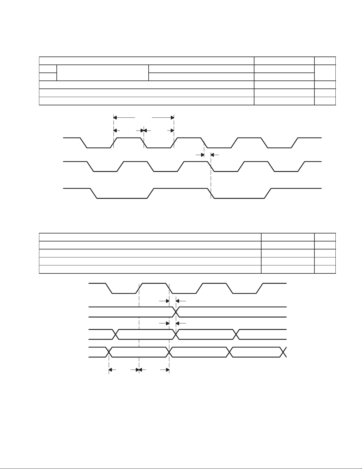
2.4 Digital-Interface Timing
t
w(1)
System-clock pulse duration, MCLK/XTI
t
w(2)
t
System-clock period, MCLK/XTI 54 ns
c(1)
Duty cycle, MCLK/XTI 40/60% 60/40%
t
Propagation delay, CLKOUT 0 10 ns
pd(1)
PARAMETER MIN TYP MAX UNIT
High 18
Low 18
t
c(1)
ns
t
w(1)
MCLK/XTI
CLKOUT
CLKOUT
(Div 2)
Figure 2−1. System-Clock Timing Requirements
2.4.1 Audio Interface (Master Mode)
PARAMETER MIN TYP MAX UNIT
t
Propagation delay, LRCIN/LRCOUT 0 10 ns
pd(2)
t
Propagation delay, DOUT 0 10 ns
pd(3)
t
Setup time, DIN 10 ns
su(1)
t
Hold time, DIN 10 ns
h(1)
BCLK
t
LRCIN
LRCOUT
pd(2)
t
pd(3)
t
w(2)
t
pd(1)
DOUT
DIN
t
su(1)
t
h(1)
Figure 2−2. Master-Mode Timing Requirements
2−5

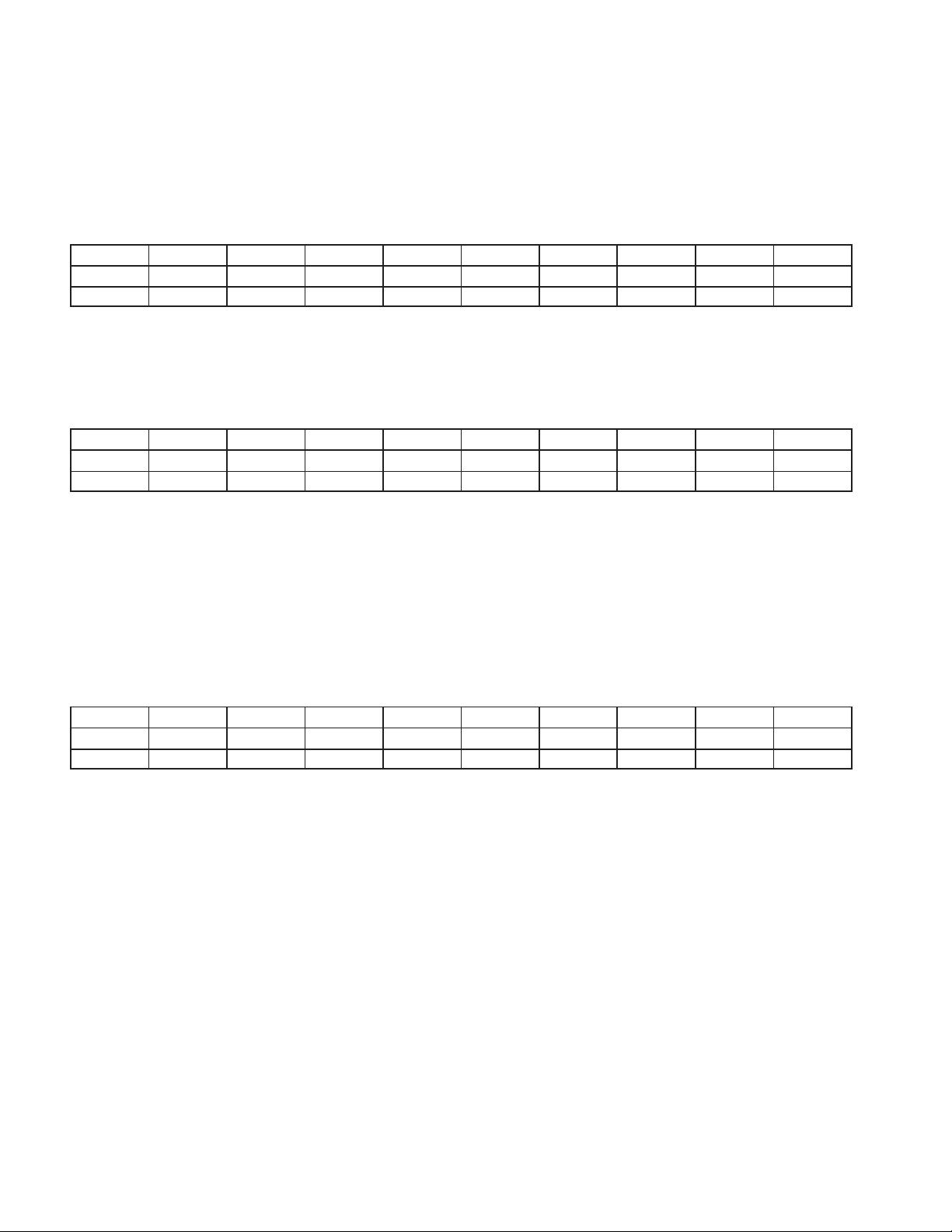
2.4.2 Audio Interface (Slave-Mode)
PARAMETER MIN TYP MAX UNIT
t
w(3)
Pulse duration, BCLK
t
w(4)
t
Clock period, BCLK 50 ns
c(2)
t
Propagation delay, DOUT 0 10 ns
pd(4)
t
Setup time, DIN 10 ns
su(2)
t
Hold time, DIN 10 ns
h(2)
t
Setup time, LRCIN 10 ns
su(3)
t
Hold time, LRCIN 10 ns
h(3)
High 20
Low 20
t
c(2)
ns
BCLK
LRCIN
LRCOUT
DIN
DOUT
t
w(4)
t
w(3)
t
su(2)
t
t
pd(2)
h(2)
Figure 2−3. Slave-Mode Timing Requirements
t
h(3)
t
su(3)
2−6

2.4.3 Three-Wire Control Interface (SDIN)
Pulse duration, CS
ns
PARAMETER MIN TYP MAX UNIT
t
w(5)
Clock pulse duration, SCLK
t
w(6)
t
Clock period, SCLK 80 ns
c(3)
t
Clock rising edge to CS rising edge, SCLK 60 ns
su(4)
t
Setup time, SDIN to SCLK 20 ns
su(5)
t
Hold time, SCLK to SDIN 20 ns
h(4)
t
w(7)
t
w(8)
CS
SCLK
High 20
Low 20
High 20
Low 20
t
c(3)
t
w(5)
t
w(6)
t
w(8)
t
su(4)
ns
t
h(4)
LSB
DIN
t
su(5)
Figure 2−4. Three-Wire Control Interface Timing Requirements
2.4.4 Two-Wire Control Interface
PARAMETER MIN TYP MAX UNIT
t
w(9)
Clock pulse duration, SCLK
t
w(10)
f(sf) Clock frequency, SCLK 0 400 kHz
t
Hold time (start condition) 600 ns
h(5)
t
Setup time (start condition) 600 ns
su(6)
t
Data hold time 900 ns
h(6)
t
Data setup time 100 ns
su(7)
t
Rise time, SDIN, SCLK 300 ns
r
t
Fall time, SDIN, SCLK 300 ns
f
t
Setup time (stop condition) 600 ns
su(8)
t
Pulse width of spikes suppressed by input filter 0 50 ns
sp
t
w(9)
SCLK
High 1.3 µs
Low 600 ns
t
w(10)
t
sp
DIN
t
h(5)
t
h(6)
t
su(7)
Figure 2−5. Two-Wire Control Interface Timing Requirements
t
su(8)
2−7

2−8

3 How to Use the TLV320AIC23B
3.1 Control Interfaces
The TLV320AIC23B has many programmable features. The control interface is used to program the registers of the
device. The control interface complies with SPI (three-wire operation) and two-wire operation specifications. The
state of the MODE terminal selects the control interface type. The MODE pin must be hardwired to the required level.
MODE INTERFACE
0 2-wire
1 SPI
3.1.1 SPI
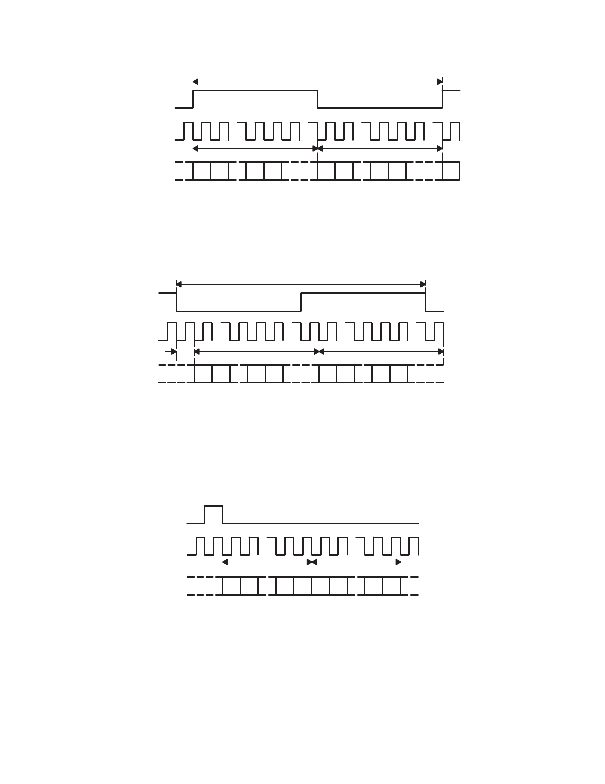
In SPI mode, SDIN carries the serial data, SCLK is the serial clock and CS latches the data word into the
TLV320AIC23B. The interface is compatible with microcontrollers and DSPs with an SPI interface.
A control word consists of 16 bits, starting with the MSB. The data bits are latched on the rising edge of SCLK. A rising
edge on CS
The control word is divided into two parts. The first part is the address block, the second part is the data block:
after the 16th rising clock edge latches the data word into the AIC (see Figure 3-1).
B[15:9] Control Address Bits
B[8:0] Control Data Bits
CS
SCLK
SDIN
B15 B14 B13 B12 B11 B10 B9 B8 B7 B6 B5 B4 B3 B2 B1 B0
MSB LSB
Figure 3−1. SPI Timing
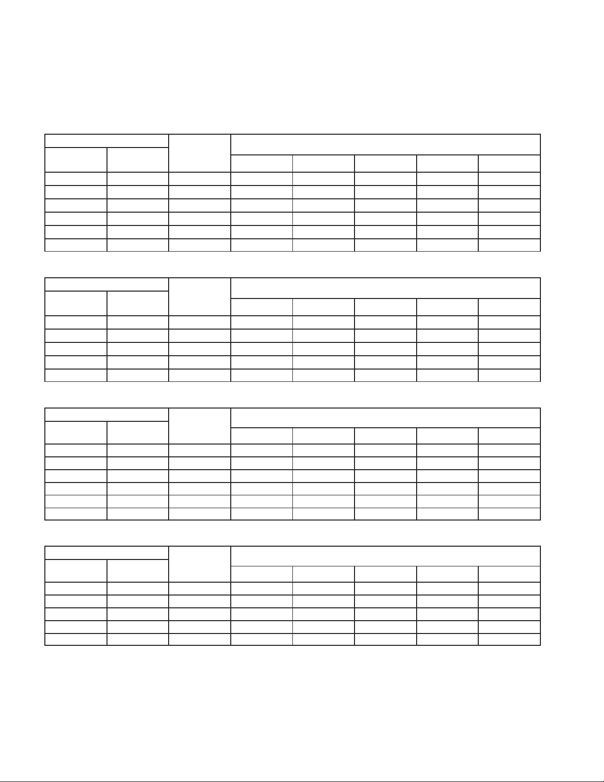
3.1.2 2-Wire
In 2-wire mode, the data transfer uses SDIN for the serial data and SCLK for the serial clock. The start condition is
a falling edge on SDIN while SCLK is high. The seven bits following the start condition determine which device on
the 2-wire bus receives the data. R/W determines the direction of the data transfer. The TL V320AIC23B is a write only
device and responds only if R/W is 0. The device operates only as a slave device whose address is selected by setting
the state of the CS pin as follows.
CS STATE
(Default = 0)
0 0011010
1 0011011
ADDRESS
3−1

The device that recognizes the address responds by pulling SDIN low during the ninth clock cycle, acknowledging
the data transfer. The control follows in the next two eight-bit blocks. The stop condition after the data transfer is a
rising edge on SDIN when SCLK is high (see Figure 3-2).
The 16-bit control word is divided into two parts. The first part is the address block, the second part is the data block:
B[15:9] Control Address Bits
B[8:0] Control Data Bits
Start Stop
SCLK
SDI
1
7891
ADDR R/W ACK B15 − B8 ACK B7 − B0 ACK
89
18
9
Figure 3−2. 2-Wire Compatible Timing
3.1.3 Register Map
The TLV320AIC23B has the following set of registers, which are used to program the modes of operation.
ADDRESS REGISTER
0000000 Left line input channel volume control
0000001 Right line input channel volume control
0000010 Left channel headphone volume control
0000011 Right channel headphone volume control
0000100 Analog audio path control
0000101 Digital audio path control
0000110 Power down control
0000111 Digital audio interface format
0001000 Sample rate control
0001001 Digital interface activation
0001111 Reset register
Left line input channel volume control (Address: 0000000)
BIT D8 D7 D6 D5 D4 D3 D2 D1 D0
Function LRS LIM X X LIV4 LIV3 LIV2 LIV1 LIV0
Default 0 1 0 0 1 0 1 1 1
LRS Left/right line simultaneous volume/mute update
Simultaneous update 0 = Disabled 1 = Enabled
LIM Left line input mute 0 = Normal 1 = Muted
LIV[4:0] Left line input volume control (10111 = 0 dB default)
11111 = +12 dB down to 00000 = –34.5 dB in 1.5-dB steps
X Reserved
3−2

Right Line Input Channel Volume Control (Address: 0000001)
BIT D8 D7 D6 D5 D4 D3 D2 D1 D0
Function RLS RIM X X RIV4 RIV3 RIV2 RIV1 RIV0
Default 0 1 0 0 1 0 1 1 1
RLS Right/left line simultaneous volume/mute update
Simultaneous update 0 = Disabled 1 = Enabled
RIM Right line input mute 0 = Normal 1 = Muted
RIV[4:0] Right line input volume control (10111 = 0 dB default)
11111 = +12 dB down to 00000 = –34.5 dB in 1.5-dB steps
X Reserved
Left Channel Headphone Volume Control (Address: 0000010)
BIT D8 D7 D6 D5 D4 D3 D2 D1 D0
Function LRS LZC LHV6 LHV5 LHV4 LHV3 LHV2 LHV1 LHV0
Default 0 1 1 1 1 1 0 0 1
LRS Left/right headphone channel simultaneous volume/mute update
Simultaneous update 0 = Disabled 1 = Enabled
LZC Left-channel zero-cross detect
Zero-cross detect 0 = Off 1 = On
LHV[6:0] Left Headphone volume control (1111001 = 0 dB default)
1111111 = +6 dB, 79 steps between +6 dB and −73 dB (mute), 0110000 = −73 dB (mute),
any thing below 0110000 does nothing − you are still muted
Right Channel Headphone Volume Control (Address: 0000011)
BIT D8 D7 D6 D5 D4 D3 D2 D1 D0
Function RLS RZC RHV6 RHV5 RHV4 RHV3 RHV2 RHV1 RHV0
Default 0 1 1 1 1 1 0 0 1
RLS Right/left headphone channel simultaneous volume/mute Update
Simultaneous update 0 = Disabled 1 = Enabled
RZC Right-channel zero-cross detect
Zero-cross detect 0 = Off 1 = On
RHV[6:0] Right headphone volume control (1111001 = 0 dB default)
1111111 = +6 dB, 79 steps between +6 dB and −73 dB (mute), 0110000 = −73 dB (mute),
any thing below 0110000 does nothing − you are still muted
Analog Audio Path Control (Address: 0000100)
BIT D8 D7 D6 D5 D4 D3 D2 D1 D0
Function STA2 STA1 STA0 STE DAC BYP INSEL MICM MICB
Default 0 0 0 0 0 1 0 1 0
STA[2:0] and STE
STE STA2 STA1 STA0 ADDED SIDETONE
1 1 X X 0 dB
1 0 0 0 −6 dB
1 0 0 1 −9 dB
1 0 1 0 −12 dB
1 0 1 1 −18 dB
0 X X X Disabled
DAC DAC select 0 = DAC off 1 = DAC selected
BYP Bypass 0 = Disabled 1 = Enabled
3−3
INSEL Input select for ADC 0 = Line 1 = Microphone
MICM Microphone mute 0 = Normal 1 = Muted
MICB Microphone boost 0=dB 1 = 20dB
X Reserved
Digital Audio Path Control (Address: 0000101)
BIT D8 D7 D6 D5 D4 D3 D2 D1 D0
Function X X X X X DACM DEEMP1 DEEMP0 ADCHP
Default 0 0 0 0 0 1 0 0 0
DACM DAC soft mute 0 = Disabled 1 = Enabled
DEEMP[1:0] De-emphasis control 00 = Disabled 01 = 32 kHz 10 = 44.1 kHz 11 = 48 kHz
ADCHP ADC high-pass filter 1 = Disabled 0 = Enabled
X Reserved
Power Down Control (Address: 0000110)
BIT D8 D7 D6 D5 D4 D3 D2 D1 D0
Function X OFF CLK OSC OUT DAC ADC MIC LINE
Default 0 0 0 0 0 0 1 1 1
OFF Device power 0 = On 1 = Off
CLK Clock 0 = On 1 = Off
OSC Oscillator 0 = On 1 = Off
OUT Outputs 0 = On 1 = Off
DAC DAC 0 = On 1 = Off
ADC ADC 0 = On 1 = Off
MIC Microphone input 0 = On 1 = Off
LINE Line input 0 = On 1 = Off
X Reserved
Digital Audio Interface Format (Address: 0000111)
BIT D8 D7 D6 D5 D4 D3 D2 D1 D0
Function X X MS LRSWAP LRP IWL1 IWL0 FOR1 FOR0
Default 0 0 0 0 0 0 0 0 1
MS Master/slave mode 0 = Slave 1 = Master
LRSWAP DAC left/right swap 0 = Disabled 1 = Enabled
LRP DAC left/right phase 0 = Right channel on, LRCIN high
1 = Right channel on, LRCIN low
DSP mode
1 = MSB is available on 2nd BCLK rising edge after LRCIN rising edge
0 = MSB is available on 1st BCLK rising edge after LRCIN rising edge
IWL[1:0] Input bit length 00 = 16 bit 01 = 20 bit 10 = 24 bit 11 = 32 bit
FOR[1:0] Data format 11 = DSP format, frame sync followed by two data words
2
10 = I
S format, MSB first, left – 1 aligned
01 = MSB first, left aligned
00 = MSB first, right aligned
X Reserved
NOTES: 1. In Master mode, the TLV320AIC23B supplies the BCLK, LRCOUT, and LRCIN. In Slave mode, BCLK, LRCOUT, and LRCIN are
supplied to the TLV320AIC23B.
2. In normal mode, BCLK = MCLK/4 for all sample rates except for 88.2 kHz and 96 kHz. For 88.2 kHz and 96 kHz sample rate,
BCLK = MCLK.
3. In USB mode, bit BCLK = MCLK
3−4
Sample Rate Control (Address: 0001000)
BIT D8 D7 D6 D5 D4 D3 D2 D1 D0
Function X CLKOUT CLKIN SR3 SR2 SR1 SR0 BOSR USB/Normal
Default 0 0 0 1 0 0 0 0 0
CLKIN Clock input divider 0 = MCLK 1 = MCLK/2
CLKOUT Clock output divider 0 = MCLK 1 = MCLK/2
SR[3:0] Sampling rate control (see Sections 3.3.2.1 AND 3.3.2.2)
BOSR Base oversampling rate
USB mode: 0 = 250 f
Normal mode: 0 = 256 f
s
s
1 = 272 f
1 = 384 f
s
s
USB/Normal Clock mode select: 0 = Normal 1 = USB
X Reserved
Digital Interface Activation (Address: 0001001)
BIT D8 D7 D6 D5 D4 D3 D2 D1 D0
Function X RES RES X X X X X ACT
Default 0 0 0 0 0 0 0 0 0
ACT Activate interface 0 = Inactive 1 = Active
X Reserved
Reset Register (Address: 0001111)
BIT D8 D7 D6 D5 D4 D3 D2 D1 D0
Function RES RES RES RES RES RES RES RES RES
Default 0 0 0 0 0 0 0 0 0
RES Write 000000000 to this register triggers reset
3.2 Analog Interface
3.2.1 Line Inputs
The TLV320AIC23B has line inputs for the left and the right audio channels (RLINEIN and LLINEIN). Both line inputs
have independently programmable volume controls and mutes. Active and passive filters for the two channels
prevent high frequencies from folding back into the audio band.
The line-input gain is logarithmically adjustable from 12 dB to –34.5 dB in 1.5-dB steps. The ADC full-scale range
is 1.0 V
it is important not to exceed the full-scale range.
The gain is independently programmable on both left and right line-inputs. To reduce the number of software write
cycles required. Both channels can be locked to the same value by setting the RLS and LRS bits (see Section 3.1.3).
The line inputs are biased internally to VMID. When the line inputs are muted or the device is set to standby mode,
the line inputs are kept biased to VMID using special antithump circuitry. This reduces audible clicks that otherwise
might be heard when reactivating the inputs.
For interfacing to a CD system, the line input should be scaled to 1 V
in Figure 3-3.
R1 and R2 divide the input signal by two, reducing the 2 V
inputs. C1 filters high-frequency noise, and C2 removes any dc component from the signal.
at A VDD = 3.3 V . The full-scale range tracks linearly with analog supply voltage AVDD. To avoid distortions,
RMS
to avoid clipping, using the circuit shown
RMS
Where:
R1 = 5 kΩ
R2 = 5 kΩ
C1 = 47 pF
C2 = 470 nF
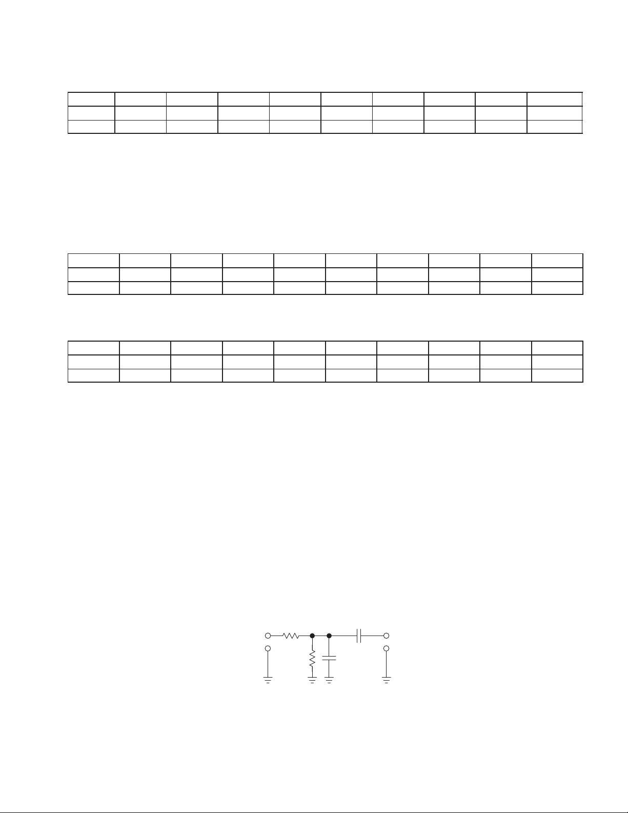
CDIN LINEIN
AGND
R1
C2 +
R
2
C1
Figure 3−3. Analog Line Input Circuit
from the CD player to the nominal 1 V
RMS
of the AIC23B
RMS
3−5

3.2.2 Microphone Input
MICIN is a high-impedance, low-capacitance input that is compatible with a wide range of microphones. It has a
programmable volume control and a mute function. Active and passive filters prevent high frequencies from folding
back into the audio band.
The MICIN signal path has two gain stages. The first stage has a nominal gain of G1 = 50 k/10 k = 5. By adding an
external resistor (R
For example, R
MIC
dB (see Section 3.1.3).
) in series with MICIN, the gain of the first stage can be adjusted by G1 = 50 k/(10 k + R
MIC
MIC
= 40 k gives a gain of 0 dB. The second stage has a software programmable gain of 0 dB or 20
50 kΩ
).
MICIN
10 kΩ
VMID
To ADC
0 dB/20 dB
Figure 3−4. Microphone Input Circuit
The microphone input is biased internally to VMID. When the line inputs are muted, the MICIN input is kept biased
to VMID using special antithump circuitry. This reduces audible clicks that may otherwise be heard when reactivating
the input.
The MICBIAS output provides a low-noise reference voltage suitable for biasing electret type microphones and the
associated external resistor biasing network. The maximum source current capability is 3 mA. This limits the smallest
value of external biasing resistors that safely can be used.
The MICBIAS output is not active in standby mode.
3.2.3 Line Outputs
The TLV320AIC23B has two low-impedance line outputs (LLINEOUT and RLINEOUT) capable of driving line loads
with 10-kΩ and 50-pF impedances.
The DAC full-scale output voltage is 1.0 V
supply voltage AV
The DAC is connected to the line outputs via a low-pass filter that removes out-of-band
DD.
components. No further external filtering is required in most applications.
The DAC outputs, line inputs, and the microphone signal are summed into the line outputs. These sources can be
switched off independently. For example, in bypass mode, the line inputs are routed to the line outputs, bypassing
the ADC and the DAC. If sidetone is enabled, the microphone signal is routed to both line outputs via a four-step
programmable attenuation circuit.
at A VDD = 3.3 V. The full-scale range tracks linearly with the analog
RMS
The line outputs are muted by either muting the DAC (analog) or soft muting (digital) and disabling the bypass and
sidetone paths (see Section 3.1.3).
3.2.4 Headphone Output
The TLV320AIC23B has stereo headphone outputs (LHPOUT and RHPOUT), and is designed to drive 16-Ω or 32-Ω
headphones. The headphone output includes a high-quality volume control and mute function.
The headphone volume is logarithmically adjustable from 6 dB to –73 dB in 1-dB steps. Writing 000000 to the
volume-control registers (see Section 3.1.3) mutes the headphone output. When the headphone output is muted or
the device is placed in standby mode, the dc voltage is maintained at the outputs to prevent audible clicks.
A zero-cross detection circuit is provided under the control of the LZC and RZC bits. If this circuit is enabled, the
volume-control values are updated only when the input signal to the gain stage is close to the analog ground level.
3−6
This minimizes audible clicks as the volume is changed or the device is muted. This circuit has no time-out, so, if only
dc levels are being applied to the gain stage input of more than 20 mV, the gain is not updated.
The gain is independently programmable on the left and right channels. Both channels can be locked to the same
value by setting the RLS and LRS bits (see Section 3.1.3).
3.2.5 Analog Bypass Mode
The TLV320AIC23B includes a bypass mode in which the analog line inputs are directly routed to the analog line
outputs, bypassing the ADC and DAC. This is enabled by selecting the bypass bit in the analog audio path control
register[see Section 3.1.3).
For a true bypass mode, the output from the DAC and the sidetone should be disabled. The line input and headphone
output volume controls and mutes are still operational in bypass mode. Therefore the line inputs, DAC output, and
microphone input can be summed together. The maximum signal at any point in the bypass path must be no greater
than 1.0V
at AVDD=3.3V to avoid clipping and distortion. This amplitude tracks linearly with AVDD.
rms
3.2.6 Sidetone Insertion
The TL V320AIC23B has a sidetone insertion made where the microphone input is routed to the line and headphone
outputs. This is useful for telephony and headset applications. The attenuation of the sidetone signal may be set to
−6 dB, −9 dB, −12 dB, −15 dB, or 0dB, by software selection (see Section 3.1.3). If this mode is used to sum the
microphone input with the DAC output and line inputs, care must be taken not to exceed signal level to avoid clipping
and distortion.
3.3 Digital Audio Interface
3.3.1 Digital Audio-Interface Modes
The TLV320AIC23B supports four audio-interface modes.
• Right justified
• Left justified
2
• I
S mode
• DSP mode
The four modes are MSB first and operate with a variable word width between 16 to 32 bits (except right-justified
mode, which does not support 32 bits).
The digital audio interface consists of clock signal BCLK, data signals DIN and DOUT, and synchronization signals
LRCIN and LRCOUT. BCLK is an output in master mode and an input in slave mode.
3.3.1.1 Right-Justified Mode
In right-justified mode, the LSB is available on the rising edge of BCLK, preceding a falling edge on LRCIN or LRCOUT
(see Figure 3-5).
LRCIN/
LRCOUT
BCLK
DIN/
DOUT
Left Channel Right Channel
n n−1 01 n−1n
MSB LSB
1/fs
1 00
Figure 3−5. Right-Justified Mode Timing
3.3.1.2 Left-Justified Mode
In left-justified mode, the MSB is available on the rising edge of BCLK, following a rising edge on LRCIN or LRCOUT
(see Figure 3-6)
3−7
LRCIN/
LRCOUT
BCLK
DIN/
DOUT
Left Channel Right Channel
n n−1 01 n−1n
MSB LSB
1/fs
1 0 n
Figure 3−6. Left-Justified Mode Timing
3.3.1.3 I2S Mode
In I2S mode, the MSB is available on the second rising edge of BCLK, after the falling edge on LRCIN or LRCOUT
(see Figure 3-7).
LRCIN/
LRCOUT
BCLK
1BCLK
DIN/
DOUT
Left Channel Right Channel
n n−1 01 n−1n
MSB LSB
1/fs
1 0
Figure 3−7. I2S Mode Timing
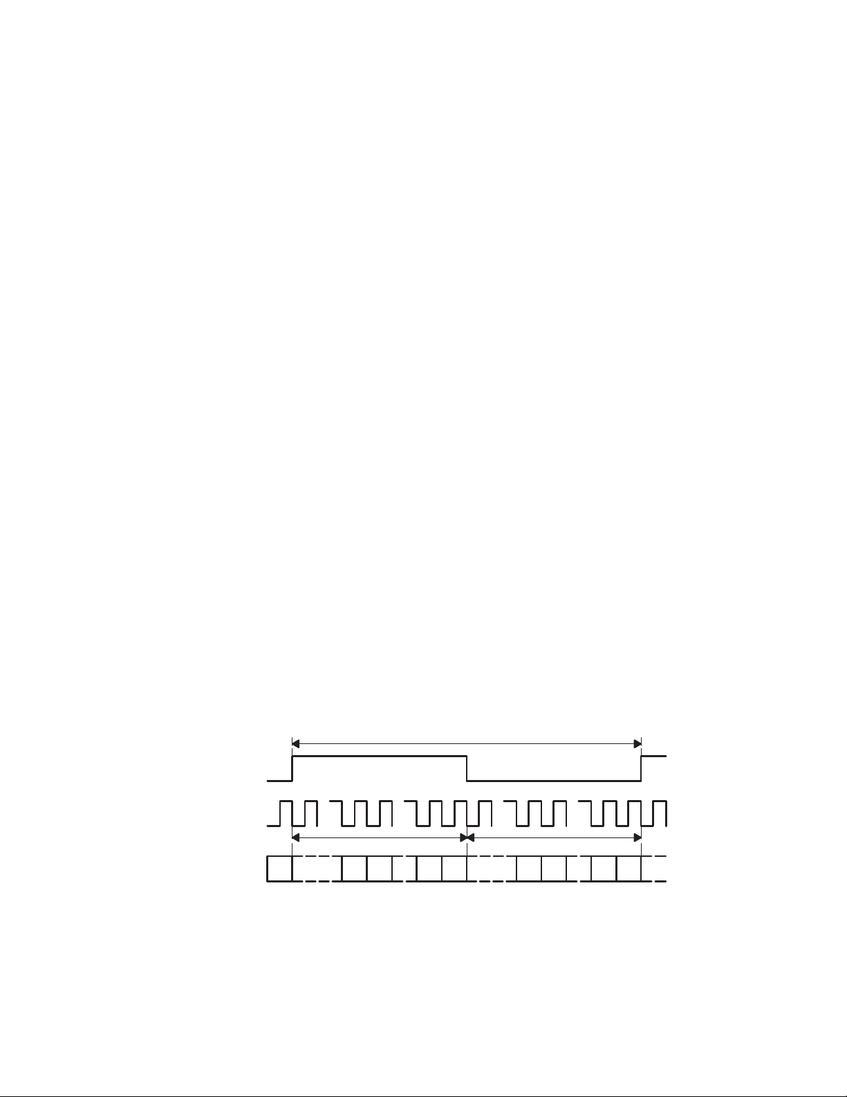
3.3.1.4 DSP Mode
The DSP mode is compatible with the McBSP ports of TI DSPs. LRCIN and LRCOUT must be connected to the Frame
Sync signal of the McBSP. A falling edge on LRCIN or LRCOUT starts the data transfer. The left-channel data consists
of the first data word, which is immediately followed by the right channel data word (see Figure 3-8). Input word length
is defined by the IWL register. Figure 3−8 shows LRP = 1 (default LRP = 0).
LRCIN/
LRCOUT
BCLK
Left Channel Right Channel
DIN/
DOUT
n n−1 01 n−1n
MSB LSB MSB LSB
1 0
Figure 3−8. DSP Mode Timing
3−8

3.3.2 Audio Sampling Rates
SAMPLING-RATE CONTROL SETTINGS
ADC
DAC
FILTER TYPE
The TLV320AIC23B can operate in master or slave clock mode. In the master mode, the TLV320AIC23B clock and
sampling rates are derived from a 12-MHz MCLK signal. This 12-MHz clock signal is compatible with the USB
specification. The TLV320AIC23B can be used directly in a USB system.
In the slave mode, an appropriate MCLK or crystal frequency and the sample rate control register settings control
the TLV320AIC23B clock and sampling rates.
The settings in the sample rate control register control the clock mode and sampling rates.
Sample Rate Control (Address: 0001000)
BIT D8 D7 D6 D5 D4 D3 D2 D1 D0
Function X CLKOUT CLKIN SR3 SR2 SR1 SR0 BOSR USB/Nor-
Default 0 0 0 1 0 0 0 0 0
CLKOUT Clock output divider 0 = MCLK 1 = MCLK/2
CLKIN Clock input divider 0 = MCLK 1 = MCLK/2
SR[3:0] Sampling rate control (see Sections 3.3.2.1 and 3.3.2.2)
BOSR Base oversampling rate
USB mode: 0 = 250 f
Normal mode: 0 = 256 f
s
s
1 = 272 f
1 = 384 f
s
s
USB/Normal Clock mode select: 0 = Normal 1 = USB
X Reserved
The clock circuit of the AIC23B has two internal dividers. The first, controlled by CLKIN, applies to the sampling-rate
generator of the codec. The second, controlled by CLKOUT, applies only to the CLKOUT terminal. By setting CLKIN
to 1, the entire codec is clocked with half the frequency, effectively dividing the resulting sampling rates by two. The
following sampling-rate tables are based on CLKIN = MCLK.
mal
3.3.2.1 USB-Mode Sampling Rates (MCLK = 12 MHz)
In the USB mode, the following ADC and DAC sampling rates are available:
SAMPLING RATE
(kHz)
96 96 3 0 1 1 1 0
88.2 88.2 2 1 1 1 1 1
48 48 0 0 0 0 0 0
44.1 44.1 1 1 0 0 0 1
32 32 0 0 1 1 0 0
8.021 8.021 1 1 0 1 1 1
8 8 0 0 0 1 1 0
48 8 0 0 0 0 1 0
44.1 8.021 1 1 0 0 1 1
8 48 0 0 0 1 0 0
8.021 44.1 1 1 0 1 0 1
†
The sampling rates are derived from the 12-MHz master clock. The available oversampling rates do not produce exactly 8-kHz, 44.1-kHz, and
88.2-kHz sampling rates, but 8.021 kHz, 44.117 kHz, and 88.235 kHz, respectively. See Figures 3−17 through 3−34 for filter responses
†
(kHz)
SR3 SR2 SR1 SR0 BOSR
3−9
3.3.2.2 Normal-Mode Sampling Rates
SAMPLING-RATE CONTROL SETTINGS
ADC
DAC
FILTER TYPE
SAMPLING-RATE CONTROL SETTINGS
ADC
DAC
FILTER TYPE
SAMPLING-RATE CONTROL SETTINGS
ADC
DAC
FILTER TYPE
SAMPLING-RATE CONTROL SETTINGS
ADC
DAC
FILTER TYPE
In normal mode, the following ADC and DAC sampling rates, depending on the MCLK frequency, are available:
MCLK = 12.288 MHz
SAMPLING RATE
(kHz)
96 96 2 0 1 1 1 0
48 48 1 0 0 0 0 0
32 32 1 0 1 1 0 0
8 8 1 0 0 1 1 0
48 8 1 0 0 0 1 0
8 48 1 0 0 1 0 0
(kHz)
SR3 SR2 SR1 SR0 BOSR
MCLK = 11.2896 MHz
SAMPLING RATE
(kHz)
88.2 88.2 2 1 1 1 1 0
44.1 44.1 1 1 0 0 0 0
8.021 8.021 1 1 0 1 1 0
44.1 8.021 1 1 0 0 1 0
8.021 44.1 1 1 0 1 0 0
(kHz)
SR3 SR2 SR1 SR0 BOSR
MCLK = 18.432 MHz
SAMPLING RATE
(kHz)
96 96 2 0 1 1 1 1
48 48 1 0 0 0 0 1
32 32 1 0 1 1 0 1
8 8 1 0 0 1 1 1
48 8 1 0 0 0 1 1
8 48 1 0 0 1 0 1
(kHz)
SR3 SR2 SR1 SR0 BOSR
MCLK = 16.9344 MHz
3−10
SAMPLING RATE
(kHz)
88.2 88.2 2 1 1 1 1 1
44.1 44.1 1 1 0 0 0 1
8.021 8.021 1 1 0 1 1 1
44.1 8.021 1 1 0 0 1 1
8.021 44.1 1 1 0 1 0 1
(kHz)
SR3 SR2 SR1 SR0 BOSR

3.3.3 Digital Filter Characteristics
PARAMETER TEST CONDITIONS MIN TYP MAX UNIT
ADC Filter Characteristics ( TI DSP 250 fs Mode Operation )
Passband ±0.05 dB 0.416 f
Stopband −6 dB 0.5 f
Passband ripple ±0.05 dB
Stopband attenuation f > 0.584 f
ADC Filter Characteristics ( TI DSP 272 fs and Normal Mode Operation )
Passband ±0.05 dB 0.4535 f
Stopband −6 dB 0.5 f
Passband ripple ±0.05 dB
Stopband attenuation f > 0.5465 f
ADC High-Pass Filter Characteristics
−3 dB, fs = 44.1 kHz 3.7 Hz
−3 dB, fs = 48 kHz 4.0 Hz
Corner frequency
DAC Filter Characteristics (48-kHz Sampling Rate)
Passband ±0.03 dB 0.416 f
Stopband −6 dB 0.5 f
Passband ripple ±0.03 dB
Stopband attenuation f > 0.584 f
DAC Filter Characteristics (44.1-kHz Sampling Rate)
Passband ±0.03 dB 0.4535 f
Stopband −6 dB 0.5 fs Hz
Passband ripple ±0.03 dB
Stopband attenuation f > 0.5465 f
−0.5 dB, fs = 44.1 kHz 10.4 Hz
−0.5 dB, fs = 48 kHz 11.3 Hz
−0.1 dB fs = 44.1 kHz 21.6 Hz
−0.1 dB, fs = 48 kHz 23.5 Hz
s
s
s
s
s
s
−60 dB
s
s
−60 dB
s
s
−50 dB
s
−50 dB
Hz
Hz
Hz
Hz
Hz
Hz
Hz
3−11
FILTER RESPONSE
vs
NORMALIZED AUDIO SAMPLING FREQUENCY
0
−2
−4
−6
Filter Response − dB
−8
−10
0 0.1 0.2 0.3
Normalized Audio Sampling Frequency
0.4 0.5
Figure 3−9. Digital De-Emphasis Filter Response − 44.1 kHz Sampling
FILTER RESPONSE
vs
NORMALIZED AUDIO SAMPLING FREQUENCY
0
−2
−4
−6
Filter Response − dB
−8
−10
0 0.10 0.20 0.30
Normalized Audio Sampling Frequency
0.40 0.50
Figure 3−10. Digital De-Emphasis Filter Response − 48 kHz Sampling
3−12

10
−10
−30
−50
Filter Response − dB
−70
FILTER RESPONSE
vs
NORMALIZED AUDIO SAMPLING FREQUENCY
−90
0 0.5 1 1.5
Normalized Audio Sampling Frequency
Figure 3−11. ADC Digital Filter Response 0: USB Mode
(Group Delay = 12 Output Samples)
FILTER RESPONSE
NORMALIZED AUDIO SAMPLING FREQUENCY
0.10
0.08
0.06
0.04
0.02
0
−0.02
−0.04
Filter Response − dB
−0.06
−0.08
−0.10
0 0.05 0.1 0.15 0.2 0.25 0.3
Normalized Audio Sampling Frequency
Figure 3−12. ADC Digital Filter Ripple 0: USB
(Group Delay = 20 Output Samples)
2 2.5 3
vs
0.35 0.4 0.45 0.5
3−13

10
−10
−30
−50
Filter Response − dB
−70
FILTER RESPONSE
vs
NORMALIZED AUDIO SAMPLING FREQUENCY
−90
0 0.5 1 1.5 2
Normalized Audio Sampling Frequency
Figure 3−13. ADC Digital Filter Response 1: USB Mode Only
FILTER RESPONSE
NORMALIZED AUDIO SAMPLING FREQUENCY
0.10
0.08
0.06
0.04
0.02
0
−0.02
−0.04
Filter Response − dB
−0.06
−0.08
−0.10
0 0.05 0.1 0.15 0.2 0.25 0.3
Normalized Audio Sampling Frequency
Figure 3−14. ADC Digital Filter Ripple 1: USB Mode Only
2.5 3
vs
0.35 0.4 0.45 0.5
3−14

FILTER RESPONSE
vs
NORMALIZED AUDIO SAMPLING FREQUENCY
10
−10
−30
−50
Filter Response − dB
−70
−90
0 0.5 1 1.5
Normalized Audio Sampling Frequency
2 2.5 3
Figure 3−15. ADC Digital Filter Response 2: USB mode and Normal Modes
(Group Delay = 3 Output Samples)
FILTER RESPONSE
vs
NORMALIZED AUDIO SAMPLING FREQUENCY
0.4
0.3
0.2
0.1
0
−0.1
−0.2
Filter Response − dB
−0.3
−0.4
0 0.05 0.1 0.15 0.2 0.25 0.3
Normalized Audio Sampling Frequency
0.35 0.4 0.45 0.5
Figure 3−16. ADC Digital Filter Ripple 2: USB Mode and Normal Modes
3−15

FILTER RESPONSE
NORMALIZED AUDIO SAMPLING FREQUENCY
10
−10
−30
−50
Filter Response − dB
−70
−90
0 0.5 1 1.5
Normalized Audio Sampling Frequency
Figure 3−17. ADC Digital Filter Response 3: USB Mode Only
FILTER RESPONSE
NORMALIZED AUDIO SAMPLING FREQUENCY
0.4
0.3
0.2
0.1
0
−0.1
−0.2
Filter Response − dB
−0.3
−0.4
0 0.05 0.10 0.15 0.20 0.25 0.30
Normalized Audio Sampling Frequency
vs
2 2.5 3
vs
0.35 0.40 0.45 0.50
3−16
Figure 3−18. ADC Digital Filter Ripple 3: USB Mode Only

FILTER RESPONSE
NORMALIZED AUDIO SAMPLING FREQUENCY
10
−10
−30
−50
Filter Response − dB
−70
−90
0 0.5 1 1.5
Normalized Audio Sampling Frequency
Figure 3−19. DAC Digital Filter Response 0: USB Mode
FILTER RESPONSE
NORMALIZED AUDIO SAMPLING FREQUENCY
0.10
0.08
0.06
0.04
0.02
0
−0.02
−0.04
Filter Response − dB
−0.06
−0.08
−0.10
0 0.05 0.1 0.15 0.2 0.25 0.3
Normalized Audio Sampling Frequency
vs
2 2.5 3
vs
0.35 0.4 0.45 0.5
Figure 3−20. DAC Digital Filter Ripple 0: USB Mode
3−17

10
−10
−30
−50
Filter Response − dB
−70
−90
0 0.5 1 1.5
Figure 3−21. DAC Digital Filter Response 1: USB Mode Only
0.10
0.08
0.06
0.04
0.02
0
−0.02
−0.04
Filter Response − dB
−0.06
−0.08
−0.10
0 0.05 0.1 0.15 0.2 0.25 0.3
FILTER RESPONSE
vs
NORMALIZED AUDIO SAMPLING FREQUENCY
2 2.5 3
Normalized Audio Sampling Frequency
FILTER RESPONSE
vs
NORMALIZED AUDIO SAMPLING FREQUENCY
0.35 0.4 0.45 0.5
Normalized Audio Sampling Frequency
3−18
Figure 3−22. DAC Digital Filter Ripple 1: USB Mode Only

FILTER RESPONSE
vs
NORMALIZED AUDIO SAMPLING FREQUENCY
10
−10
−30
−50
Filter Response − dB
−70
−90
0 0.5 1 1.5
Normalized Audio Sampling Frequency
2 2.5 3
Figure 3−23. DAC Digital Filter Response 2: USB Mode and Normal Modes
FILTER RESPONSE
vs
NORMALIZED AUDIO SAMPLING FREQUENCY
0.4
0.3
0.2
0.1
0
−0.1
−0.2
Filter Response − dB
−0.3
−0.4
0 0.05 0.1 0.15 0.2 0.25 0.3
Normalized Audio Sampling Frequency
0.35 0.4 0.45 0.5
Figure 3−24. DAC Digital Filter Ripple 2: USB Mode and Normal Modes
3−19

FILTER RESPONSE
NORMALIZED AUDIO SAMPLING FREQUENCY
10
−10
−30
−50
Filter Response − dB
−70
−90
0 0.5 1 1.5
Normalized Audio Sampling Frequency
Figure 3−25. DAC Digital Filter Response 3: USB Mode Only
FILTER RESPONSE
NORMALIZED AUDIO SAMPLING FREQUENCY
0.4
0.3
0.2
0.1
0
−0.1
Filter Response − dB
−0.2
−0.3
−0.4
0 0.05 0.1 0.15 0.2 0.25 0.3
Normalized Audio Sampling Frequency
vs
2 2.5 3
vs
0.35 0.4 0.45 0.5
Figure 3−26. DAC Digital Filter Ripple 3: USB Mode Only
The delay between the converter is a function of the sample rate. The group delays for the AIC23B are shown in the
following table. Each delay is one LR clock (1/sample rate).
Table 3−1. Group Dealys
FILTER GROUP DELAY
DAC type 0 11
DAC type 1 18
DAC type 2 5
DAC type 3 5
ADC type 0 12
ADC type 1 20
ADC type 2 3
ADC type 3 6
3−20

Appendix A
Mechanical Data
GQE/ZQE (S-PBGA-N80) PLASTIC BALL GRID ARRAY
0,68
0,62
5,10
4,90
0,35
0,25
SQ
∅ 0,05
4,00 TYP
0,50
J
H
G
F
E
D
C
B
A
321
4
1,00 MAX
Seating Plane
M
0,21
0,11
0,08
98765
4200461/C 10/00
0,50
NOTES: A. All linear dimensions are in millimeters.
B. This drawing is subject to change without notice.
C. MicroStar Junior BGA configuration
D. Falls within JEDEC MO-225
MicroStar Junior is a trademark of Texas Instruments.
A−1

PW (R-PDSO-G**) PLASTIC SMALL-OUTLINE PACKAGE
14 PINS SHOWN
0,65
1,20 MAX
14
0,30
0,19
8
4,50
4,30
PINS **
7
0,15
0,05
8
14
1
A
DIM
M
0,10
6,60
6,20
Seating Plane
0,10
0,15 NOM
0°−ā 8°
2016
Gage Plane
24
0,25
0,75
0,50
28
A MAX
A MIN
NOTES: A. All linear dimensions are in millimeters.
B. This drawing is subject to change without notice.
C. Body dimensions do not include mold flash or protrusion not to exceed 0,15.
D. Falls within JEDEC MO-153
A−2
3,10
2,90
5,10
4,90
5,10
4,90
6,60
6,40
7,90
7,70
9,80
9,60
4040064/F 01/97
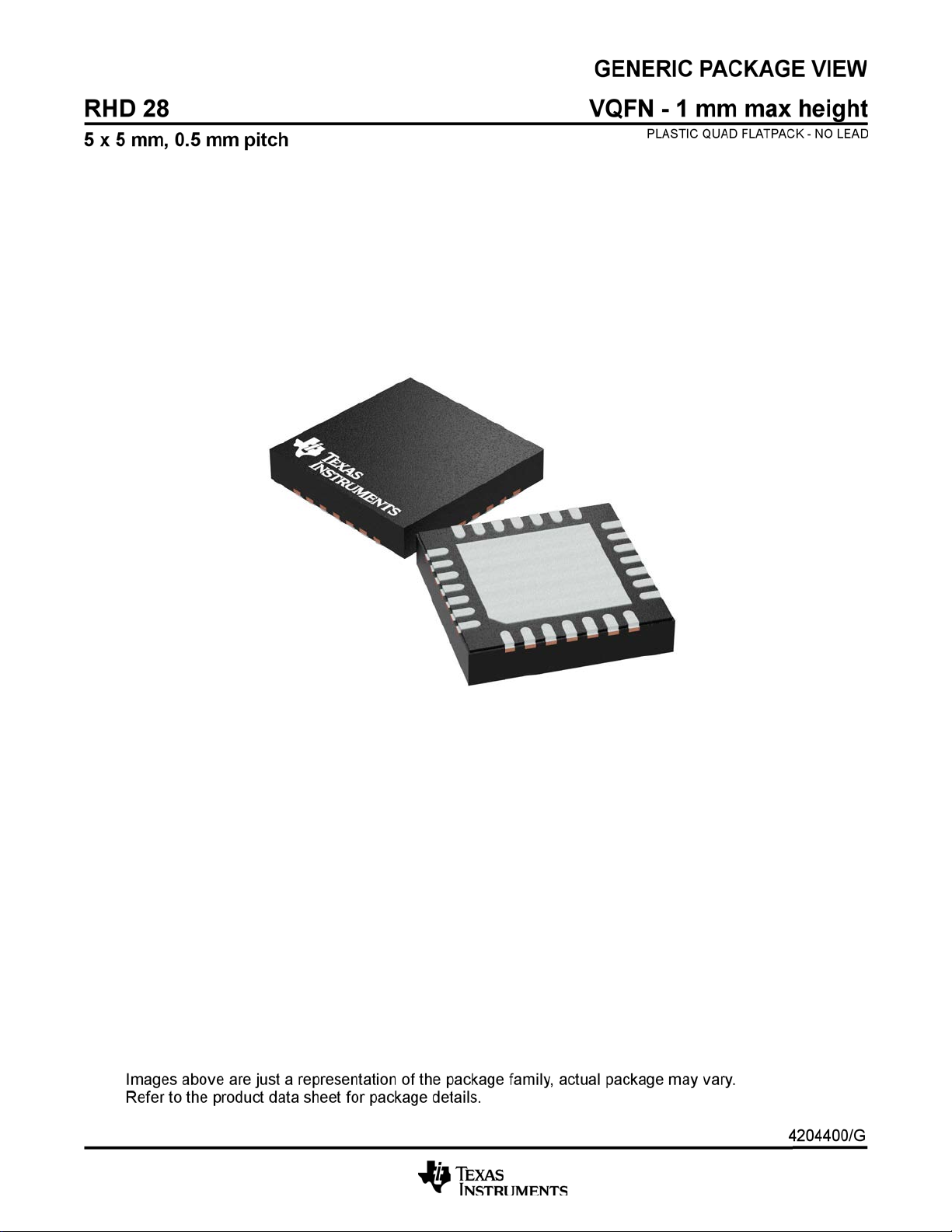
RHD (S−PQFP−N28) PLASTIC QUAD FLATPACK
1,00
0,80
0,08
C
PIN 1
IDENTIFIER
A
B
5,00
28
PIN 1
INDEX AREA
5,00
1
0,20 REF
C
SEATING PLANE
3,25
SQ
3,00
1
0,05 MAX
28
0,65
0,45
0,435
0,18
0,18
NOTES: A. All linear dimensions are in millimeters.
B. This drawing is subject to change without notice.
C. QFN (Quad Flatpack No−Lead) Package configuration.
D. The Package thermal performance may be enhanced by bonding the thermal die pad to
an external thermal plane. This pad is electrically and thermally connected to the backside
of the die and possibly selected ground leads.
E. Package complies to JEDEC MO-220.
0,435
EXPOSED THERMAL
DIE PAD
D
28
28
0,30
0,18
0,10
M
C A B
3,00
4
0,50
4204400/A 05/02
A−3
PACKAGE OPTION ADDENDUM
www.ti.com
PACKAGING INFORMATION
Orderable Device Status
TLV320AIC23BIPW ACTIVE TSSOP PW 28 50 RoHS & Green NIPDAU Level-1-260C-UNLIM -40 to 85 AIC23BI
TLV320AIC23BIPWG4 ACTIVE TSSOP PW 28 50 RoHS & Green NIPDAU Level-1-260C-UNLIM -40 to 85 AIC23BI
TLV320AIC23BIPWR ACTIVE TSSOP PW 28 2000 RoHS & Green NIPDAU Level-1-260C-UNLIM -40 to 85 AIC23BI
TLV320AIC23BIPWRG4 ACTIVE TSSOP PW 28 2000 RoHS & Green NIPDAU Level-1-260C-UNLIM -40 to 85 AIC23BI
TLV320AIC23BIRHD ACTIVE VQFN RHD 28 73 RoHS & Green NIPDAU Level-2-260C-1 YEAR -40 to 85 AIC23BI
TLV320AIC23BIRHDG4 ACTIVE VQFN RHD 28 73 RoHS & Green NIPDAU Level-2-260C-1 YEAR -40 to 85 AIC23BI
TLV320AIC23BIRHDR ACTIVE VQFN RHD 28 3000 RoHS & Green NIPDAU Level-2-260C-1 YEAR -40 to 85 AIC23BI
TLV320AIC23BPW ACTIVE TSSOP PW 28 50 RoHS & Green NIPDAU Level-1-260C-UNLIM -10 to 70 AIC23B
TLV320AIC23BPWG4 ACTIVE TSSOP PW 28 50 RoHS & Green NIPDAU Level-1-260C-UNLIM -10 to 70 AIC23B
TLV320AIC23BPWR ACTIVE TSSOP PW 28 2000 RoHS & Green NIPDAU Level-1-260C-UNLIM -10 to 70 AIC23B
TLV320AIC23BRHD ACTIVE VQFN RHD 28 73 RoHS & Green NIPDAU Level-2-260C-1 YEAR -10 to 70 AIC23B
Package Type Package
(1)
Drawing
Pins Package
Qty
Eco Plan
(2)
Lead finish/
Ball material
(6)
MSL Peak Temp
(3)
Op Temp (°C) Device Marking
15-Jan-2021
Samples
(4/5)
TLV320AIC23BRHDR ACTIVE VQFN RHD 28 3000 RoHS & Green NIPDAU Level-2-260C-1 YEAR -10 to 70 AIC23B
(1)
The marketing status values are defined as follows:
ACTIVE: Product device recommended for new designs.
LIFEBUY: TI has announced that the device will be discontinued, and a lifetime-buy period is in effect.
NRND: Not recommended for new designs. Device is in production to support existing customers, but TI does not recommend using this part in a new design.
PREVIEW: Device has been announced but is not in production. Samples may or may not be available.
OBSOLETE: TI has discontinued the production of the device.
(2)
RoHS: TI defines "RoHS" to mean semiconductor products that are compliant with the current EU RoHS requirements for all 10 RoHS substances, including the requirement that RoHS substance
do not exceed 0.1% by weight in homogeneous materials. Where designed to be soldered at high temperatures, "RoHS" products are suitable for use in specified lead-free processes. TI may
reference these types of products as "Pb-Free".
RoHS Exempt: TI defines "RoHS Exempt" to mean products that contain lead but are compliant with EU RoHS pursuant to a specific EU RoHS exemption.
Green: TI defines "Green" to mean the content of Chlorine (Cl) and Bromine (Br) based flame retardants meet JS709B low halogen requirements of <=1000ppm threshold. Antimony trioxide based
flame retardants must also meet the <=1000ppm threshold requirement.
Addendum-Page 1

PACKAGE OPTION ADDENDUM
www.ti.com
(3)
MSL, Peak Temp. - The Moisture Sensitivity Level rating according to the JEDEC industry standard classifications, and peak solder temperature.
15-Jan-2021
(4)
There may be additional marking, which relates to the logo, the lot trace code information, or the environmental category on the device.
(5)
Multiple Device Markings will be inside parentheses. Only one Device Marking contained in parentheses and separated by a "~" will appear on a device. If a line is indented then it is a continuation
of the previous line and the two combined represent the entire Device Marking for that device.
(6)
Lead finish/Ball material - Orderable Devices may have multiple material finish options. Finish options are separated by a vertical ruled line. Lead finish/Ball material values may wrap to two
lines if the finish value exceeds the maximum column width.
Important Information and Disclaimer:The information provided on this page represents TI's knowledge and belief as of the date that it is provided. TI bases its knowledge and belief on information
provided by third parties, and makes no representation or warranty as to the accuracy of such information. Efforts are underway to better integrate information from third parties. TI has taken and
continues to take reasonable steps to provide representative and accurate information but may not have conducted destructive testing or chemical analysis on incoming materials and chemicals.
TI and TI suppliers consider certain information to be proprietary, and thus CAS numbers and other limited information may not be available for release.
In no event shall TI's liability arising out of such information exceed the total purchase price of the TI part(s) at issue in this document sold by TI to Customer on an annual basis.
OTHER QUALIFIED VERSIONS OF TLV320AIC23B :
Automotive: TLV320AIC23B-Q1
•
NOTE: Qualified Version Definitions:
Automotive - Q100 devices qualified for high-reliability automotive applications targeting zero defects
•
Addendum-Page 2

PACKAGE MATERIALS INFORMATION
www.ti.com 13-Jan-2021
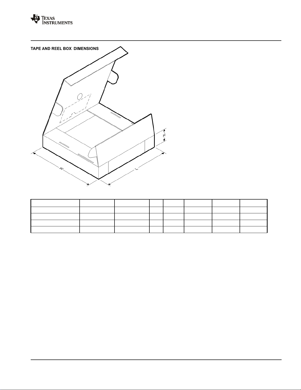
TAPE AND REEL INFORMATION
*All dimensions are nominal
Device Package
TLV320AIC23BIPWR TSSOP PW 28 2000 330.0 16.4 6.9 10.2 1.8 12.0 16.0 Q1
TLV320AIC23BIRHDR VQFN RHD 28 3000 330.0 12.4 5.3 5.3 1.5 8.0 12.0 Q2
TLV320AIC23BPWR TSSOP PW 28 2000 330.0 16.4 6.9 10.2 1.8 12.0 16.0 Q1
TLV320AIC23BRHDR VQFN RHD 28 3000 330.0 12.4 5.3 5.3 1.5 8.0 12.0 Q2
Type
Package
Drawing
Pins SPQ Reel
Diameter
(mm)
Reel
Width
W1 (mm)
A0
(mm)B0(mm)K0(mm)P1(mm)W(mm)
Pin1
Quadrant
Pack Materials-Page 1
PACKAGE MATERIALS INFORMATION
www.ti.com 13-Jan-2021
*All dimensions are nominal
Device PackageType Package Drawing Pins SPQ Length (mm) Width (mm) Height (mm)
TLV320AIC23BIPWR TSSOP PW 28 2000 350.0 350.0 43.0
TLV320AIC23BIRHDR VQFN RHD 28 3000 350.0 350.0 43.0
TLV320AIC23BPWR TSSOP PW 28 2000 350.0 350.0 43.0
TLV320AIC23BRHDR VQFN RHD 28 3000 350.0 350.0 43.0
Pack Materials-Page 2

PACKAGE OUTLINE
PIN 1 INDEX AREA
1.0
0.8
SCALE 2.500
B
5.15
4.85
VQFN - 1 mm max heightRHD0028B
PLASTIC QUAD FLATPACK - NO LEAD
A
5.15
4.85
C
SEATING PLANE
0.05
0.00
EXPOSED
THERMAL PAD
2X 3
24X 0.5
PIN 1 ID
SYMM
3.15 0.1
2X 3
SYMM
8
7
29
1
28
28X
14
15
21
22
0.65
0.45
0.08 C
3.15 0.1
0.30
28X
0.18
(0.2) TYP
0.1 C A B
0.05
4226146/A 08/2020
NOTES:
1. All linear dimensions are in millimeters. Any dimensions in parenthesis are for reference only. Dimensioning and tolerancing
per ASME Y14.5M.
2. This drawing is subject to change without notice.
3. The package thermal pad must be soldered to the printed circuit board for thermal and mechanical performance.
www.ti.com

28X (0.75)
28
( 3.15)
SYMM
EXAMPLE BOARD LAYOUT
VQFN - 1 mm max heightRHD0028B
PLASTIC QUAD FLATPACK - NO LEAD
22
SEE SOLDER MASK
DETAIL
28X (0.24)
24X (0.5)
(R0.05) TYP
( 0.2) TYP
ALL AROUND
1
7
VIA
0.07 MAX
29
8
(1.325)
(4.65)
LAND PATTERN EXAMPLE
EXPOSED METAL SHOWN
SCALE: 18X
METAL EDGE
21
SYMM
(4.65)
(1.325)
15
14
0.07 MIN
ALL AROUND
METAL UNDER
SOLDER MASK
EXPOSED METAL
NON SOLDER MASK
DEFINED
(PREFERRED)
SOLDER MASK
OPENING
EXPOSED
METAL
SOLDER MASK DEFINED
SOLDER MASK
OPENING
SOLDER MASK DETAILS
4226146/A 08/2020
NOTES: (continued)
4. This package is designed to be soldered to a thermal pad on the board. For more information, see Texas Instruments literature
number SLUA271 (www.ti.com/lit/slua271).
5. Vias are optional depending on application, refer to device data sheet. If any vias are implemented, refer to their locations shown
on this view. It is recommended that vias under paste be filled, plugged or tented.
www.ti.com

28X (0.75)
28
EXAMPLE STENCIL DESIGN
VQFN - 1 mm max heightRHD0028B
PLASTIC QUAD FLATPACK - NO LEAD
(0.785) TYP
22
28X (0.24)
24X (0.5)
SYMM
(R0.05) TYP
1
29
7
8
4X (1.37)
SYMM
14
21
(0.785) TYP
(4.65)
4X (1.37)
15
(4.65)
SOLDER PASTE EXAMPLE
BASED ON 0.125 MM THICK STENCIL
76% PRINTED SOLDER COVERAGE BY AREA UNDER PACKAGE
NOTES: (continued)
6. Laser cutting apertures with trapezoidal walls and rounded corners may offer better paste release. IPC-7525 may have alternate
design recommendations.
SCALE: 20X
EXPOSED PAD 29
4226146/A 08/2020
www.ti.com


IMPORTANT NOTICE AND DISCLAIMER
TI PROVIDES TECHNICAL AND RELIABILITY DATA (INCLUDING DATASHEETS), DESIGN RESOURCES (INCLUDING REFERENCE
DESIGNS), APPLICATION OR OTHER DESIGN ADVICE, WEB TOOLS, SAFETY INFORMATION, AND OTHER RESOURCES “AS IS”
AND WITH ALL FAULTS, AND DISCLAIMS ALL WARRANTIES, EXPRESS AND IMPLIED, INCLUDING WITHOUT LIMITATION ANY
IMPLIED WARRANTIES OF MERCHANTABILITY, FITNESS FOR A PARTICULAR PURPOSE OR NON-INFRINGEMENT OF THIRD
PARTY INTELLECTUAL PROPERTY RIGHTS.
These resources are intended for skilled developers designing with TI products. You are solely responsible for (1) selecting the appropriate
TI products for your application, (2) designing, validating and testing your application, and (3) ensuring your application meets applicable
standards, and any other safety, security, or other requirements. These resources are subject to change without notice. TI grants you
permission to use these resources only for development of an application that uses the TI products described in the resource. Other
reproduction and display of these resources is prohibited. No license is granted to any other TI intellectual property right or to any third party
intellectual property right. TI disclaims responsibility for, and you will fully indemnify TI and its representatives against, any claims, damages,
costs, losses, and liabilities arising out of your use of these resources.
TI’s products are provided subject to TI’s Terms of Sale (https:www.ti.com/legal/termsofsale.html) or other applicable terms available either
on ti.com or provided in conjunction with such TI products. TI’s provision of these resources does not expand or otherwise alter TI’s
applicable warranties or warranty disclaimers for TI products.IMPORTANT NOTICE
Mailing Address: Texas Instruments, Post Office Box 655303, Dallas, Texas 75265
Copyright © 2021, Texas Instruments Incorporated
 Loading...