

Texas Instruments TLV2773CDR, TLV2773CDGSR, TLV2773CDGS, TLV2773CD, TLV2773AIN Datasheet
...
TLV277x, TLV277xA
FAMILY OF 2.7-V HIGH-SLEW-RATE RAIL-TO-RAIL OUTPUT
OPERATIONAL AMPLIFIERS WITH SHUTDOWN
SLOS209D – JANUARY 1998 – REVISED NOVEMBER 1999
1
POST OFFICE BOX 655303 • DALLAS, TEXAS 75265
D
High Slew Rate . . . 10.5 V/µs Typ
D
High-Gain Bandwidth . . . 5.1 MHz Typ
D
Supply Voltage Range 2.5 V to 5.5 V
D
Rail-to-Rail Output
D
360 µV Input Offset Voltage
D
Low Distortion Driving 600-Ω
0.005% THD+N
D
1 mA Supply Current (Per Channel)
D
17 nV/√Hz Input Noise Voltage
D
2 pA Input Bias Current
D
Characterized from TA = –40°C to 125°C
D
Available in MSOP and SOT-23 Packages
D
Micropower Shutdown Mode ...IDD < 1 µA
description
The TLV277x CMOS operational amplifier family combines high slew rate and bandwidth, rail-to-rail output
swing, high output drive, and excellent dc precision. The device provides 10.5 V/µs of slew rate and 5.1 MHz
of bandwidth while only consuming 1 mA of supply current per channel. This ac performance is much higher
than current competitive CMOS amplifiers. The rail-to-rail output swing and high output drive make these
devices a good choice for driving the analog input or reference of analog-to-digital converters. These devices
also have low distortion while driving a 600-Ω load for use in telecom systems.
These amplifiers have a 360 µV input offset voltage, a 17 nV/√Hz input noise voltage, and a 2 pA input bias
current for measurement, medical, and industrial applications. The TL V277x family is also specified across an
extended temperature range (–40°C to 125°C), making it useful for automotive systems.
These devices operate from a 2.5 V to 5.5 V single supply voltage and are characterized at 2.7 V and 5 V . The
single-supply operation and low power consumption make these devices a good solution for portable
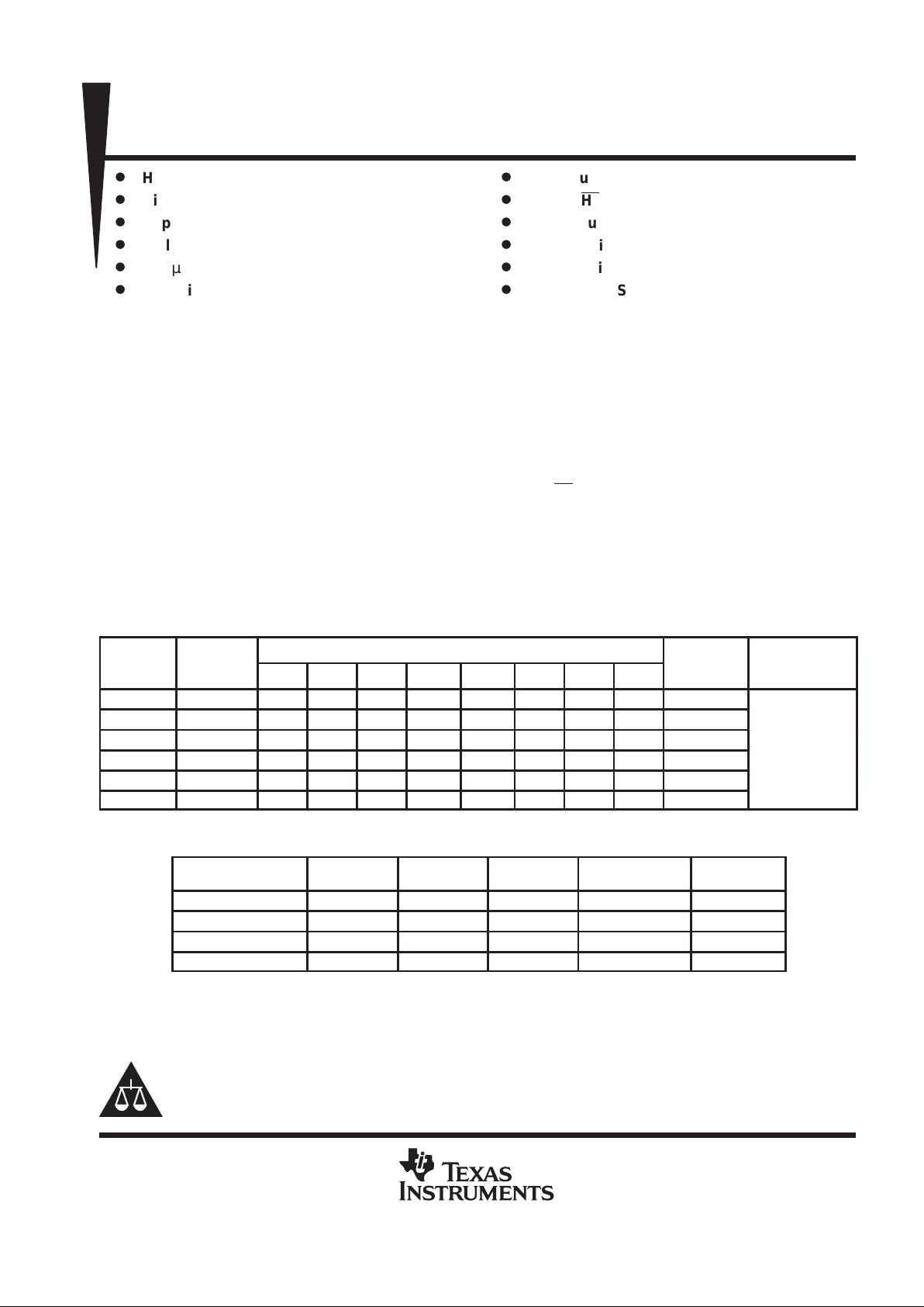
applications. The following table lists the packages available.
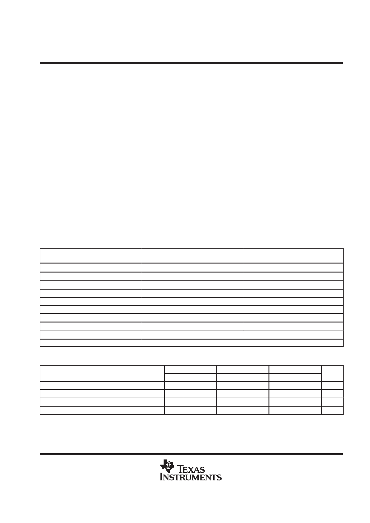
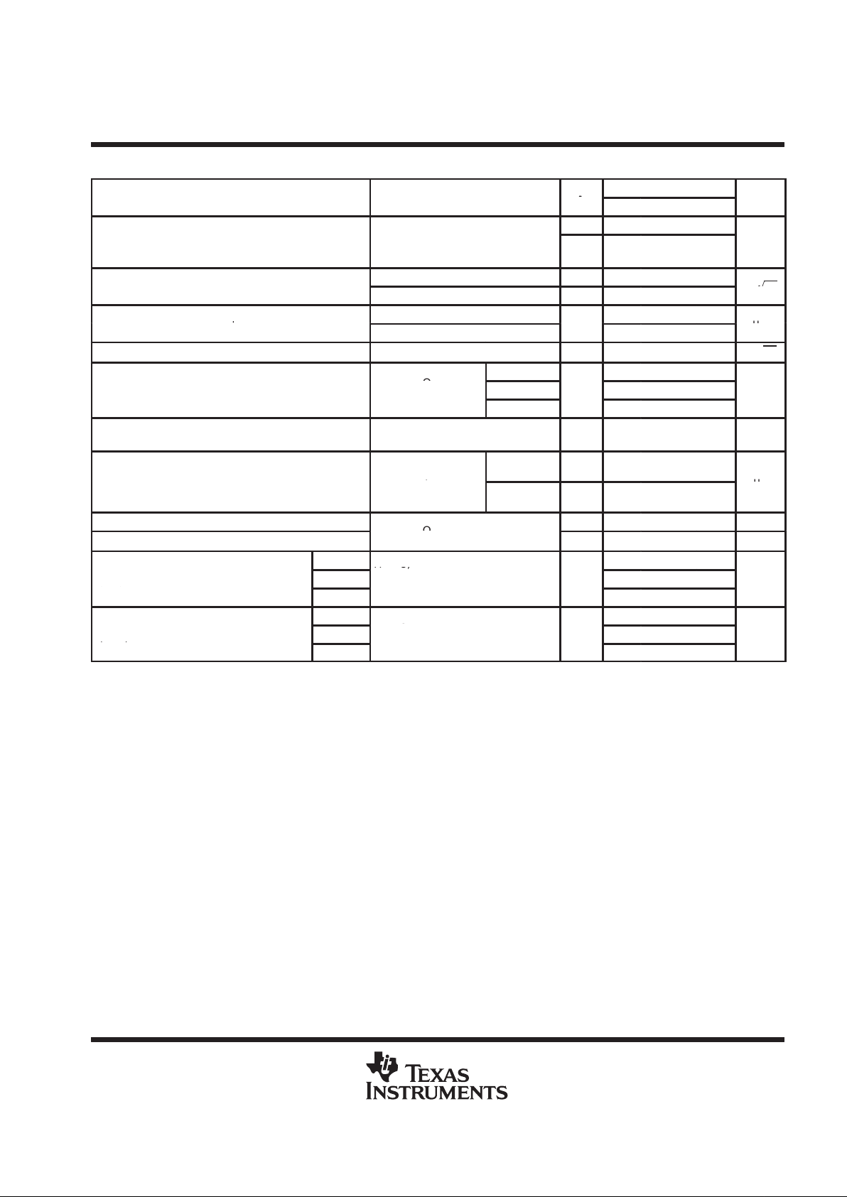
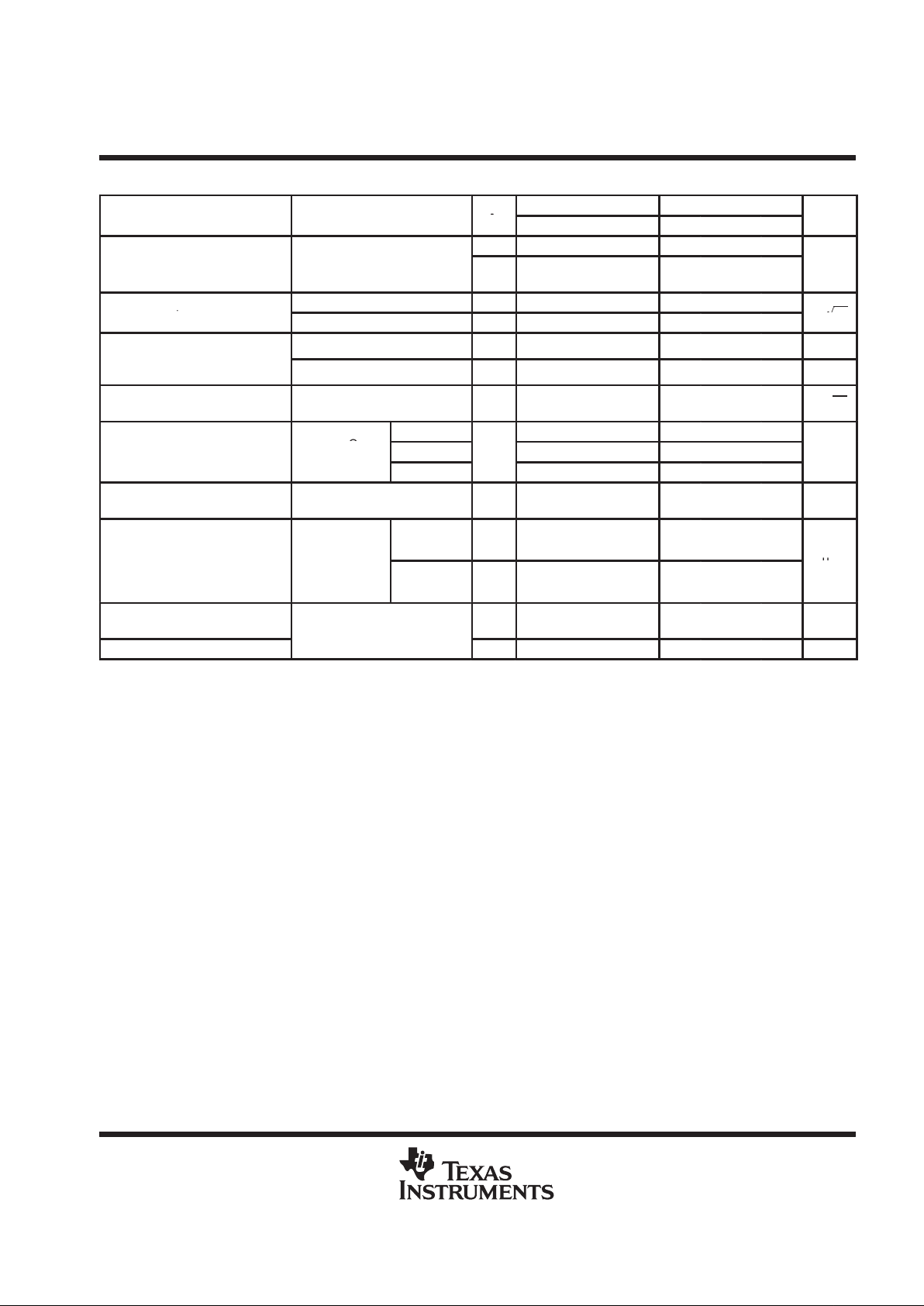
FAMILY PACKAGE TABLE
NUMBER
PACKAGE TYPES
UNIVERSAL
DEVICE
OF
CHANNELS
PDIP CDIP SOIC SOT-23 TSSOP MSOP LCCC CPAK
SHUTDOWN
EVM BOARD
TLV2770 1 8 — 8 — — 8 — — Yes
TLV2771 1 — — 8 5 — — — — —
TLV2772 2 8 8 8 — — 8 20 10 —
Refer to the EVM
TLV2773 2 14 — 14 — — 10 — — Yes
Selecti
on Guide
(
Lit# SLOU060
)
TLV2774 4 14 — 14 — 14 — — — —
(Lit# SLOU060)
TLV2775 4 16 — 16 — 16 — — — Yes
A SELECTION OF SINGLE-SUPPLY OPERATIONAL AMPLIFIER PRODUCTS
§
DEVICE
V
DD
(V)
BW
(MHz)
SLEW RATE
(V/µs)
IDD (per channel)
(µA)
RAIL-TO-RAIL
TLV277X 2.5 – 6.0 5.1 10.5 1000 O
TLV247X 2.7 – 6.0 2.8 1.5 600 I/O
TLV245X 2.7 – 6.0 0.22 0.11 23 I/O
TLV246X 2.7 – 6.0 6.4 1.6 550 I/O
§
All specifications measured at 5 V .
Please be aware that an important notice concerning availability, standard warranty, and use in critical applications of
Texas Instruments semiconductor products and disclaimers thereto appears at the end of this data sheet.
PRODUCTION DATA information is current as of publication date.
Products conform to specifications per the terms of Texas Instruments
standard warranty. Production processing does not necessarily include
testing of all parameters.
Copyright 1999, Texas Instruments Incorporated
TLV277x, TLV277xA
FAMILY OF 2.7-V HIGH-SLEW-RATE RAIL-TO-RAIL OUTPUT
OPERATIONAL AMPLIFIERS WITH SHUTDOWN
SLOS209D – JANUARY 1998 – REVISED NOVEMBER 1999
2
POST OFFICE BOX 655303 • DALLAS, TEXAS 75265
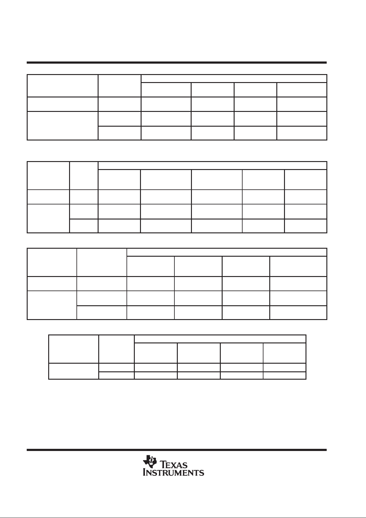
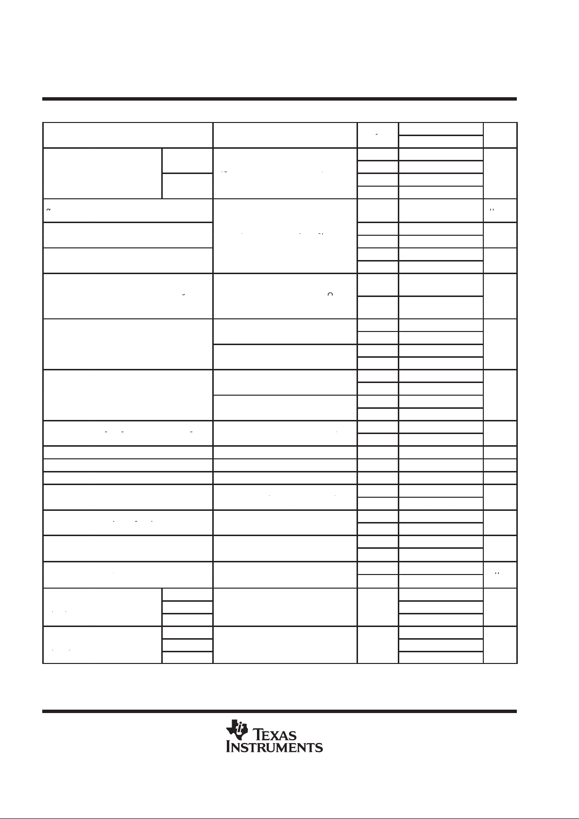
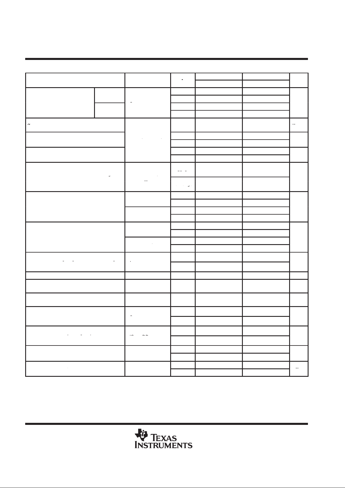
TLV2770 and TLV2771 AVAILABLE OPTIONS
°
PACKAGED DEVICES
T
A
VIOmax AT 25°C
(mV)
SMALL OUTLINE
(D)
SOT-23
(DBV)
MSOP
(DGK)
PLASTIC DIP
(P)
0°C to 70°C 2.5
TLV2770CD
TLV2771CD
—
TLV2771CDBV
TLV2770CDGK
†
—
TLV2770CP
—
°
°
2.5
TLV2770ID
TLV2771ID
—
TLV2771IDBV
TLV2770IDGK
†
—
TLV2770IP
—
–
40°C to 125°C
1.6
TLV2770AID
TLV2771AID
—
—
—
—
TLV2770AIP
—
†
This device is in the Product Preview stage of development. Please contact your local TI sales office for availability.
TLV2772 and TLV2773 AVAILABLE OPTIONS
PACKAGED DEVICES
T
A
VIOmax
AT 25°C
(mV)
SMALL
OUTLINE
(D)
MSOP
(DGK)
MSOP
(DGS)
PLASTIC DIP
(N)
PLASTIC DIP
(P)
0°C to 70°C 2.5
TLV2772CD
TLV2773CD
TLV2772CDGK
—
—
TLV2773CDGS
—
TLV2773CN
TLV2772CP
—
°
°
2.5
TLV2772ID
TLV2773ID
TLV2772IDGK
—
—
TLV2773IDGS
—
TLV2773IN
TLV2772IP
—
–
40°C to 125°C
1.6
TLV2772AID
TLV2773AID
—
—
—
—
—
TLV2773AIN
TLV2772AIP
—
TLV2774 and TLV2775 AVAILABLE OPTIONS
PACKAGED DEVICES
T
A
VIOmax AT 25°C
(mV)
SMALL
OUTLINE
(D)
PLASTIC DIP
(N)
PLASTIC DIP
(P)
TSSOP
(PW)
0°C to 70°C 2.7
TLV2774CD
TLV2775CD
—
TLV2775CN
TLV2774CP
—
TLV2774CPW
TLV2775CPW
°
°
2.7
TLV2774ID
TLV2775ID
—
TLV2775IN
TLV2774IP
—
TLV2774IPW
TLV2775IPW
–
40°C to 125°C
2.1
TLV2774AID
TLV2775AID
—
TLV2775AIN
TLV2774AIP
—
TLV2774AIPW
TLV2775AIPW
TLV2772M AND TLV2772AM AVAILABLE OPTIONS
PACKAGED DEVICES
T
A
VIOmax
AT 25°C
(mV)
SMALL
OUTLINE
(D)
CHIP CARRIER
(FK)
CERAMIC DIP
(JG)
CERAMIC
FLATPACK
(U)
°
°
2.5 TLV2772MD TLV2772MFK TLV2772MJG TLV2772MU
–
55°C to 125°C
1.6 TLV2772AMD TLV2772AMFK TLV2772AMJG TLV2772AMU
TLV277x, TLV277xA
FAMILY OF 2.7-V HIGH-SLEW-RATE RAIL-TO-RAIL OUTPUT
OPERATIONAL AMPLIFIERS WITH SHUTDOWN
SLOS209D – JANUARY 1998 – REVISED NOVEMBER 1999
3
POST OFFICE BOX 655303 • DALLAS, TEXAS 75265
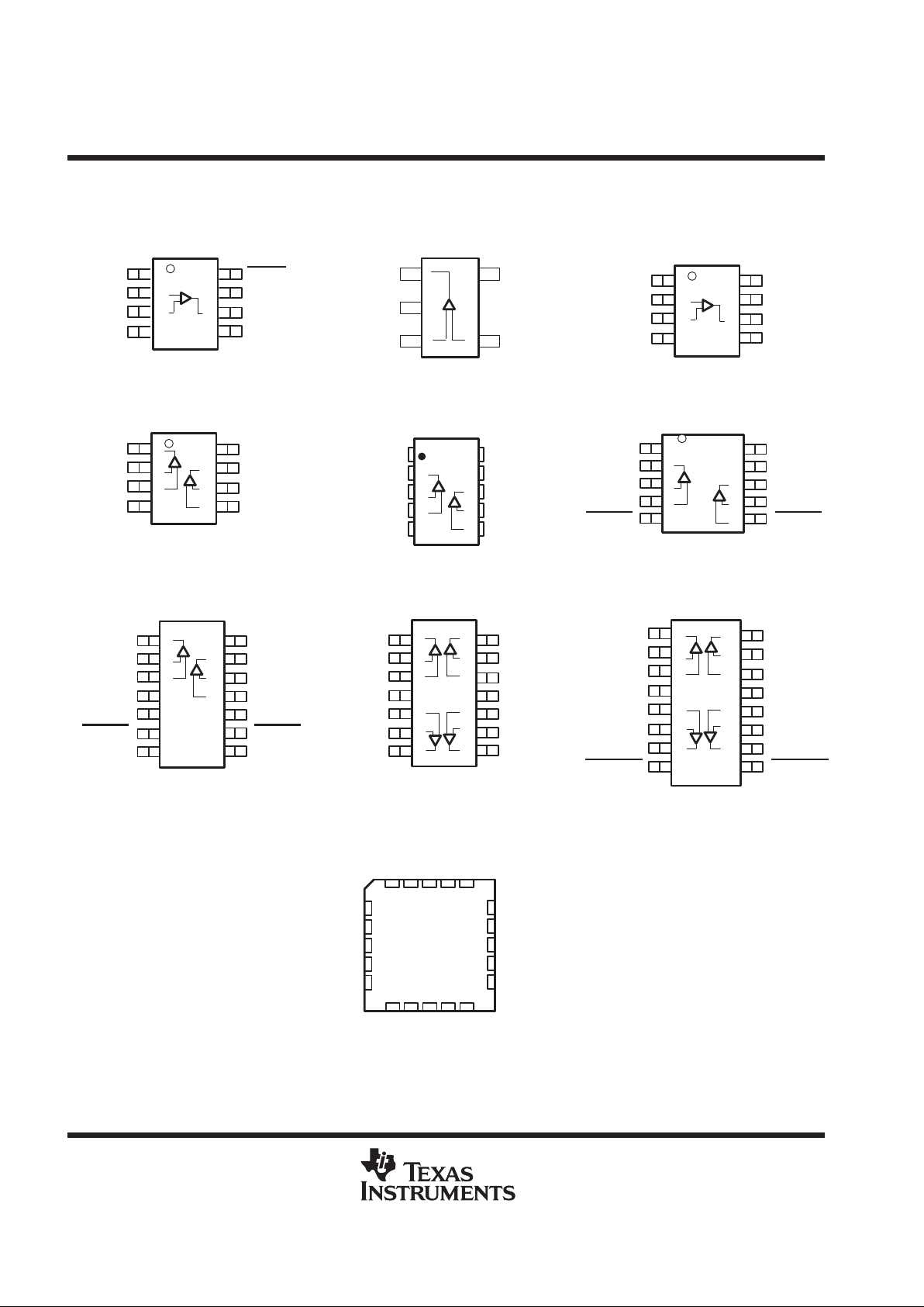
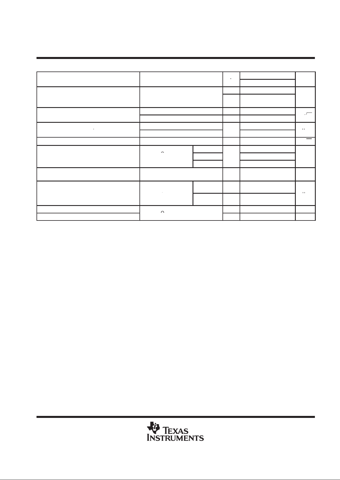
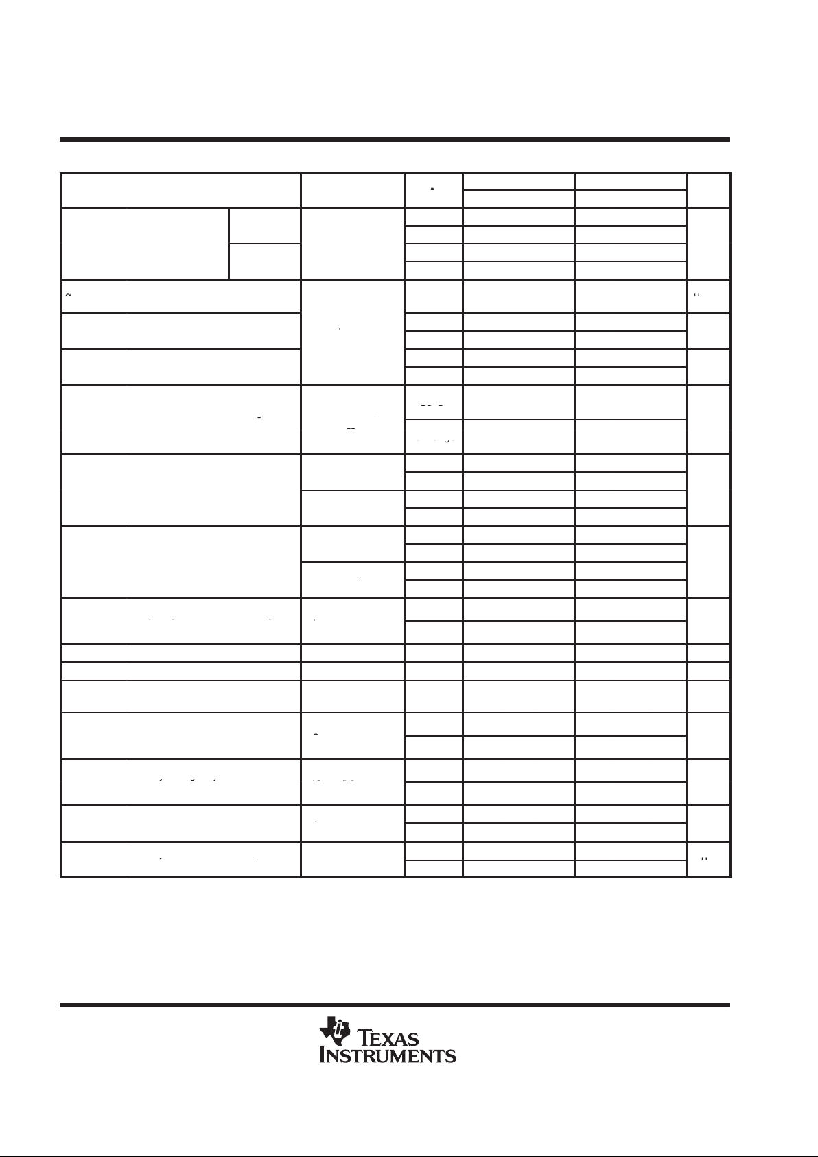
PACKAGE SYMBOLS
PACKAGE TYPE
PINS PART NUMBER SYMBOL
†
TLV2771CDBV VAMC
SOT23
5 Pin
TLV2771IDBV VAMI
TLV2770CDGK xxTIABO
TLV2770IDGK xxTIABP
8 Pin
TLV2772CDGK xxTIAAF
MSOP
TLV2772IDGK xxTIAAG
TLV2773CDGS xxTIABQ
10 Pin
TLV2773IDGS xxTIABR
†
xx represents the device date code.
TLV277x, TLV277xA
FAMILY OF 2.7-V HIGH-SLEW-RATE RAIL-TO-RAIL OUTPUT
OPERATIONAL AMPLIFIERS WITH SHUTDOWN
SLOS209D – JANUARY 1998 – REVISED NOVEMBER 1999
4
POST OFFICE BOX 655303 • DALLAS, TEXAS 75265
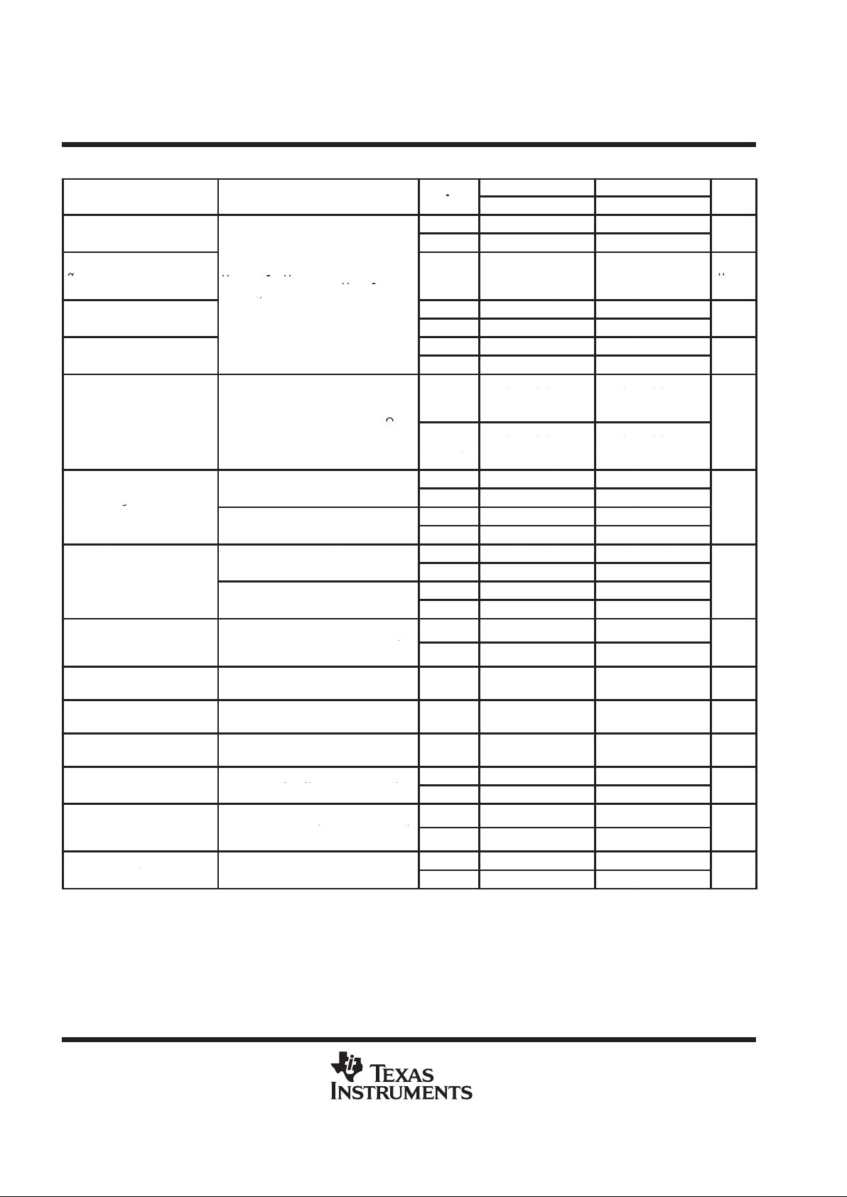
TLV277x P ACKAGE PINOUTS
1
2
3
4
5
10
9
8
7
6
1OUT
1IN–
1IN+
GND
1SHDN
V
DD
2OUT
2IN–
2IN+
2SHDN
3
2
4
5
(TOP VIEW)
1
OUT
GND
IN+
V
DD
IN–
TLV2771
DBV PACKAGE
TLV2773
DGS PACKAGE
(TOP VIEW)
NC – No internal connection
1
2
3
4
8
7
6
5
1OUT
1IN–
1IN+
GND
V
DD
2OUT
2IN–
2IN+
TLV2772
D, DGK†, JG, OR P PACKAGE
(TOP VIEW)
1
2
3
4
8
7
6
5
NC
IN–
IN+
GND
SHDN
V
DD
OUT
NC
TLV2770
D, DGK† OR P PACKAGE
(TOP VIEW)
1
2
3
4
8
7
6
5
NC
IN–
IN+
GND
NC
V
DD
OUT
NC
TLV2771
D PACKAGE
(TOP VIEW)
1
2
3
4
5
6
7
14
13
12
11
10
9
8
1OUT
1IN–
1IN+
GND
NC
1SHDN
NC
V
DD
2OUT
2IN–
2IN+
NC
2SHDN
NC
(TOP VIEW)
TLV2773
D OR N PACKAGE
1
2
3
4
5
6
7
14
13
12
11
10
9
8
1OUT
1IN–
1IN+
V
DD
2IN+
2IN–
2OUT
4OUT
4IN–
4IN+
GND
3IN+
3IN–
3OUT
(TOP VIEW)
TLV2774
D, N, OR PW PACKAGE
1
2
3
4
5
6
7
8
16
15
14
13
12
11
10
9
1OUT
1IN–
1IN+
V
DD
2IN+
2IN–
2OUT
1/2SHDN
4OUT
4IN–
4IN+
GND
3IN+
3IN–
3OUT
3/4SHDN
(TOP VIEW)
TLV2775
D, N, OR PW PACKAGE
NC
V
DD
+
2OUT
2IN –
2IN +
NC
1OUT
1IN –
1IN +
GND
1
2
3
4
5
10
9
8
7
6
(TOP VIEW)
TLV2772M AND TLV2772AM
U PACKAGE
3212019
910111213
4
5
6
7
8
18
17
16
15
14
NC
2OUT
NC
2IN–
NC
NC
1IN–
NC
1IN+
NC
NC
1OUT
NC
2IN+
NC
NC
NC
NC
V
DD+
TLV2772M AND TLV2772AM
FK PACKAGE
(TOP VIEW)
GND
†
This device is in the Product Preview stage of development. Please contact your local TI sales office for availability.
TLV277x, TLV277xA
FAMILY OF 2.7-V HIGH-SLEW-RATE RAIL-TO-RAIL OUTPUT
OPERATIONAL AMPLIFIERS WITH SHUTDOWN
SLOS209D – JANUARY 1998 – REVISED NOVEMBER 1999
5
POST OFFICE BOX 655303 • DALLAS, TEXAS 75265
absolute maximum ratings over operating free-air temperature range (unless otherwise noted)
†
Supply voltage, VDD (see Note 1) 7 V. . . . . . . . . . . . . . . . . . . . . . . . . . . . . . . . . . . . . . . . . . . . . . . . . . . . . . . . . . . . .
Differential input voltage, VID (see Note 2) ±V
DD
. . . . . . . . . . . . . . . . . . . . . . . . . . . . . . . . . . . . . . . . . . . . . . . . . . .
Input voltage range, V
I
(any input, see Note 1) –0.3 V to V
DD
. . . . . . . . . . . . . . . . . . . . . . . . . . . . . . . . . . . . . . . .
Input current, II (any input) ±4 mA. . . . . . . . . . . . . . . . . . . . . . . . . . . . . . . . . . . . . . . . . . . . . . . . . . . . . . . . . . . . . . . .
Output current, IO ±50 mA. . . . . . . . . . . . . . . . . . . . . . . . . . . . . . . . . . . . . . . . . . . . . . . . . . . . . . . . . . . . . . . . . . . . . . .
Total current into V
DD+
±50 mA. . . . . . . . . . . . . . . . . . . . . . . . . . . . . . . . . . . . . . . . . . . . . . . . . . . . . . . . . . . . . . . . . .
Total current out of GND ±50 mA. . . . . . . . . . . . . . . . . . . . . . . . . . . . . . . . . . . . . . . . . . . . . . . . . . . . . . . . . . . . . . . .
Duration of short-circuit current (at or below) 25°C (see Note 3) unlimited. . . . . . . . . . . . . . . . . . . . . . . . . . . . . .
Continuous total power dissipation See Dissipation Rating Table. . . . . . . . . . . . . . . . . . . . . . . . . . . . . . . . . . . . .
Operating free-air temperature range, T
A
: C suffix 0°C to 70°C. . . . . . . . . . . . . . . . . . . . . . . . . . . . . . . . . . . . . .
I suffix –40°C to 125°C. . . . . . . . . . . . . . . . . . . . . . . . . . . . . . . . . . . .
M suffix –55°C to 125°C. . . . . . . . . . . . . . . . . . . . . . . . . . . . . . . . . .
Storage temperature range, T
stg
–65°C to 150°C. . . . . . . . . . . . . . . . . . . . . . . . . . . . . . . . . . . . . . . . . . . . . . . . . . .
Lead temperature 1,6 mm (1/16 inch) from case for 10 seconds 260°C. . . . . . . . . . . . . . . . . . . . . . . . . . . . . . .
†
Stresses beyond those listed under “absolute maximum ratings” may cause permanent damage to the device. These are stress ratings only, and
functional operation of the device at these or any other conditions beyond those indicated under “recommended operating conditions” is not
implied. Exposure to absolute-maximum-rated conditions for extended periods may affect device reliability.
NOTES: 1. All voltage values, except differential voltages, are with respect to GND.
2. Differential voltages are at the noninverting input with respect to the inverting input. Excessive current flows when input is brought
below GND – 0.3 V.
3. The output may be shorted to either supply. Temperature and /or supply voltages must be limited to ensure that the maximum
dissipation rating is not exceeded.
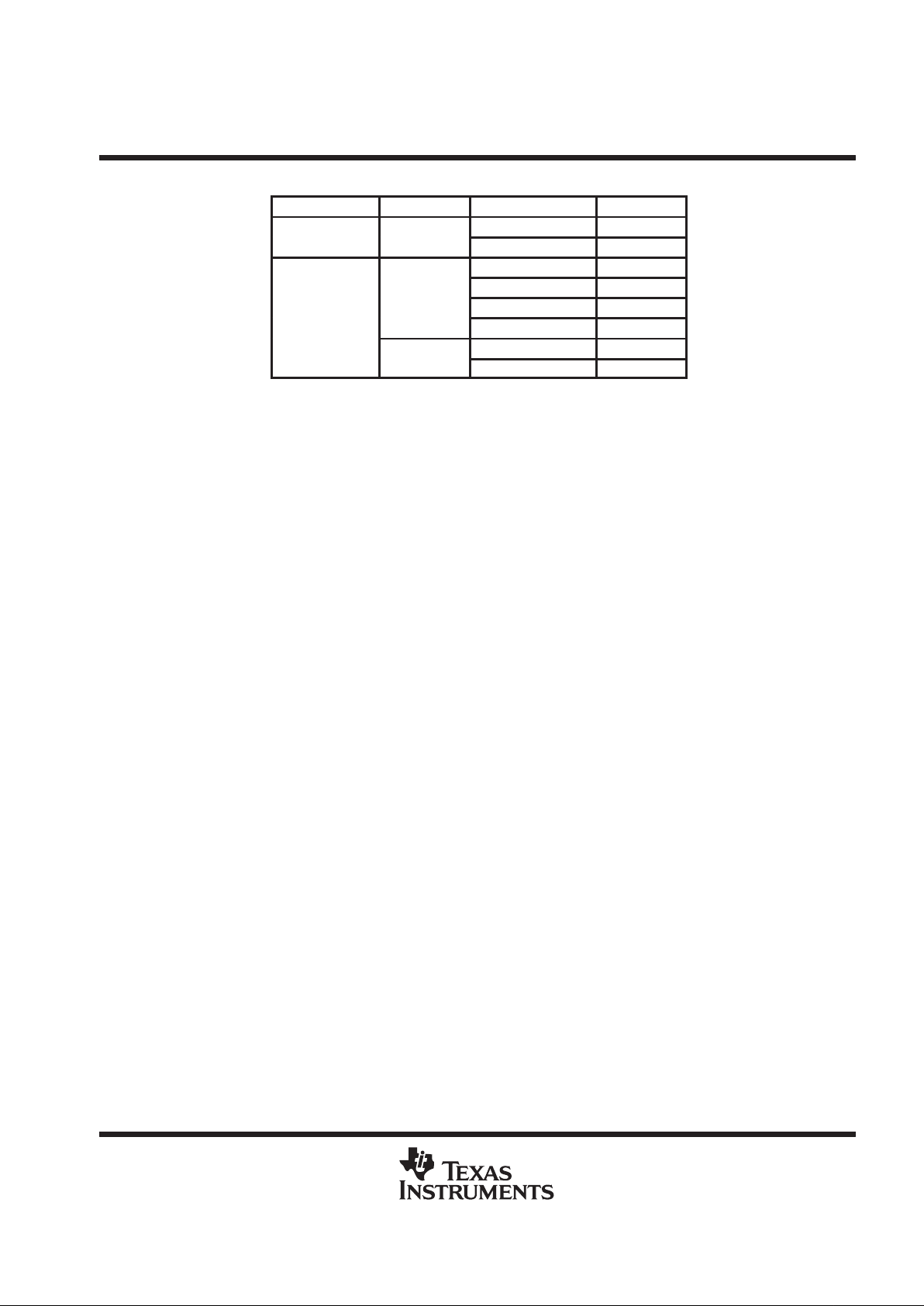
DISSIPATION RATING TABLE
T
≤ 25°C DERATING FACT OR T
= 70°C T
= 85°C T
= 125°C
PACKAGE
A
POWER RATING ABOVE TA = 25°CAPOWER RATINGAPOWER RATINGAPOWER RATING
D 725 mW 5.8 mW/°C 464 mW 377 mW 145 mW
DBV 437 mW 3.5 mW/°C 280 mW 227 mW 87 mW
DGK 424 mW 3.4 mW/°C 271 mW 220 mW 85 mW
DGS 424 mW 3.4 mW/°C 271 mW 220 mW 85 mW
FK 1375 mW 11.0 mW/°C 672 mW 546 mW 210 mW
JG 1050 mW 8.4 mW/°C 880 mW 714 mW 275 mW
N 1150 mW 9.2 mW/°C 736 mW 598 mW 230 mW
P 1000 mW 8.0 mW/°C 640 mW 520 mW 200 mW
PW 700 mW 5.6 mW/°C 448 mW 364 mW 140 mW
U 675 mW 5.4 mW/°C 432 mW 350 mW 135 mW
recommended operating conditions
C SUFFIX I SUFFIX M SUFFIX
MIN MAX MIN MAX MIN MAX
UNIT
Supply voltage, V
DD
2.5 6 2.5 6 2.5 6 V
Input voltage range, V
I
GND V
DD+
–1.3 GND V
DD+
–1.3 GND V
DD+
–1.3 V
Common-mode input voltage, V
IC
GND V
DD+
–1.3 GND V
DD+
–1.3 GND V
DD+
–1.3 V
Operating free-air temperature, T
A
0 70 –40 125 –55 125 °C
TLV277x, TLV277xA
FAMILY OF 2.7-V HIGH-SLEW-RATE RAIL-TO-RAIL OUTPUT
OPERATIONAL AMPLIFIERS WITH SHUTDOWN
SLOS209D – JANUARY 1998 – REVISED NOVEMBER 1999
6
POST OFFICE BOX 655303 • DALLAS, TEXAS 75265
electrical characteristics at specified free-air temperature, VDD = 2.7 V (unless otherwise noted)
TLV277xC
PARAMETER
TEST CONDITIONS
T
A
†
MIN TYP MAX
UNIT
25°C 0.44 2.5
p
TLV2770/1/2
VIC = 0,
V
= 0,
Full range
0.47 2.7
VIOInput offset voltage
IC
RS = 50 Ω,
O
,
VDD = ±1.35 V
25°C
0.8 2.7
mV
TLV2773/4/5
Full range 0.86 2.9
Temperature coefficient of input 25°C to
°
α
VIO
offset voltage 125°C
2µV/°C
p
V
= 0,
V
= 0
,
25°C 1
p
IIOInput offset current
IC
,
RS = 50 Ω
V
O
0,
VDD = ±1.35 V
Full range
2 100
pA
p
25°C 2
p
IIBInput bias current
Full range 6 100
pA
Common-mode input voltage
25°C
0
to 1.4
–0.3
to 1.7
V
ICR
g
range
CMRR
> 70 dB,
R
S
=
50 Ω
Full range
0
to 1.4
–0.3
to 1.7
V
25°C 2.6
p
I
OH
= –
0.675 mA
Full range 2.5
VOHHigh-level output voltage
25°C 2.4
V
I
OH
= –2.2
mA
Full range 2.1
25°C 0.1
p
V
IC
= 1.35 V,
I
OL
= 0.
675 mA
Full range 0.2
VOLLow-level output voltage
25°C 0.21
V
V
IC
=
1.35 V
,
I
OL
=
2.2 mA
Full range 0.6
Large-signal differential voltage V
= 1.35 V ,
R
= 10 kΩ,
25°C 20 380
A
VD
gg g
amplification
IC
,
VO = 0.6 V to 2.1 V
L
,
Full range 13
V/mV
r
i(d)
Differential input resistance 25°C 10
12
Ω
c
i(c)
Common-mode input capacitance f = 10 kHz 25°C 8 pF
z
o
Closed-loop output impedance f = 100 kHz, AV = 10 25°C 25 Ω
V
= 0 to 1.5 V, V
= 1.5 V,
25°C 70 84
CMRR
Common-mode rejection ratio
IC
,
RS = 50 Ω
O
,
Full range 70 82
dB
Supply voltage rejection ratio V
= 2.7 V to 5 V, V
= V
/2,
25°C 70 89
k
SVR
ygj
(∆VDD /∆VIO)
DD
,
No load
IC DD
,
Full range 70 84
dB
pp
p
25°C 1 2
IDDSupply current (per channel)
V
O
=
1.5 V
,
No load
Full range 2
mA
Supply current in shutdown (per
25°C 0.8 1.5
I
DD(SHDN)
y(
channel)
Full range 1.3 2
µ
A
TLV2770 1.47
V
(ON)
Turnon voltage
TLV2773
AV = 5 25°C
1.43
V
()
level
TLV2775 1.40
TLV2770 1.27
V
(OFF)
Turnoff voltage
TLV2773
AV = 5 25°C
1.21
V
()
level
TLV2775 1.20
†
Full range is 0°C to 70°C.
TLV277x, TLV277xA
FAMILY OF 2.7-V HIGH-SLEW-RATE RAIL-TO-RAIL OUTPUT
OPERATIONAL AMPLIFIERS WITH SHUTDOWN
SLOS209D – JANUARY 1998 – REVISED NOVEMBER 1999
7
POST OFFICE BOX 655303 • DALLAS, TEXAS 75265
operating characteristics at specified free-air temperature, VDD = 2.7 V (unless otherwise noted)
TLV277xC
PARAMETER
TEST CONDITIONS
T
A
†
MIN TYP MAX
UNIT
p
25°C
5 9
SR Slew rate at unity gain
V
O(PP)
= 0.8 V,
RL = 10 kΩ
C
L
=
100 pF
,
Full
range
4.7 6
V/µs
p
f = 1 kHz 25°C 21
VnEquivalent input noise voltage
f = 10 kHz 25°C 17
n
V/√H
z
Peak-to-peak equivalent input noise
f = 0.1 Hz to 1 Hz
°
0.33
V
N(PP)
q
voltage
f = 0.1 Hz to 10 Hz
25°C
0.86
µ
V
I
n
Equivalent input noise current f = 100 Hz 25°C 0.6
fA/√Hz
AV = 1 0.0085%
THD + N Total harmonic distortion plus noise
RL = 600 Ω,
AV = 10
25°C
0.025%
f = 1 kHz
AV = 100 0.12%
Gain-bandwidth product
f = 10 kHz,
CL = 100 pF
RL = 600 Ω,
25°C 4.8 MHz
AV = –1,
Step = 1 V ,
0.1% 25°C 0.186
tsSettling time
,
RL = 600 Ω,
CL = 100 pF
0.01% 25°C 0.3
µ
s
φ
m
Phase margin at unity gain
p
25°C 46°
Gain margin
R
L
=
600 Ω
,
C
L
=
100 pF
25°C 12 dB
†
Full range is 0°C to 70°C.
TLV277x, TLV277xA
FAMILY OF 2.7-V HIGH-SLEW-RATE RAIL-TO-RAIL OUTPUT
OPERATIONAL AMPLIFIERS WITH SHUTDOWN
SLOS209D – JANUARY 1998 – REVISED NOVEMBER 1999
8
POST OFFICE BOX 655303 • DALLAS, TEXAS 75265
electrical characteristics at specified free-air temperature, VDD = 5 V (unless otherwise noted)
TLV277xC
PARAMETER
TEST CONDITIONS
T
A
†
MIN TYP MAX
UNIT
25°C 0.36 2.5
p
TLV2770/1/2
VIC = 0,
V
= 0,
Full range
0.4 2.7
VIOInput offset voltage
IC
RS = 50 Ω
O
,
VDD = ±2.5 V
25°C
0.7 2.5
mV
TLV2773/4/5
Full range 0.78 2.7
Temperature coefficient of input 25°C to
°
α
VIO
offset voltage 125°C
2µV/°C
p
V
= 0,
V
= 0
,
25°C 1
p
IIOInput offset current
IC
,
RS = 50 Ω
V
O
0,
VDD = ±2.5 V
Full range
2 100
pA
p
25°C 2
p
IIBInput bias current
Full range 6 100
pA
p
25°C
0
to 3.7
–0.3
to 3.8
V
ICR
Common-mode input voltage range
CMRR
> 60 dB,
R
S
= 50
Ω
Full range
0
to 3.7
–0.3
to 3.8
V
25°C 4.9
p
I
OH
= –1.3
mA
Full range 4.8
VOHHigh-level output voltage
25°C 4.7
V
I
OH
= –4.2
mA
Full range 4.4
25°C 0.1
p
V
IC
=
2.5 V
,
I
OL
=
1.3 mA
Full range 0.2
VOLLow-level output voltage
25°C 0.21
V
V
IC
= 2.5 V,
I
OL
= 4.2
mA
Full range 0.6
Large-signal differential voltage V
= 2.5 V,
R
= 10 kΩ,
25°C 20 450
A
VD
gg g
amplification
IC
,
VO = 1 V to 4 V
L
,
Full range 13
V/mV
r
i(d)
Differential input resistance 25°C 10
12
Ω
c
i(c)
Common-mode input capacitance f = 10 kHz 25°C 8 pF
z
o
Closed-loop output impedance f = 100 kHz, AV = 10 25°C 20 Ω
V
= 0 to 3.7 V, V
= 3.7 V,
25°C 60 96
CMRR
Common-mode rejection ratio
IC
,
RS = 50 Ω
O
,
Full range 60 93
dB
Supply voltage rejection ratio V
= 2.7 V to 5 V, V
= V
/2,
25°C 70 89
k
SVR
ygj
(∆VDD /∆VIO)
DD
,
No load
IC DD
,
Full range 70 84
dB
pp
p
25°C 1 2
IDDSupply current (per channel)
V
O
= 1.5 V,
No load
Full range 2
mA
Supply current in shutdown (per
25°C 0.8 1.5
I
DD(SHDN)
y(
channel)
Full range 1.3 2
µ
A
TLV2770 2.59
V
(ON)
Turnon voltage level
TLV2773
AV = 5 25°C
2.47
V
()
TLV2775 2.48
TLV2770 2.41
V
(OFF)
Turnoff voltage level
TLV2773
AV = 5 25°C
2.32
V
()
TLV2775 2.29
†
Full range is 0°C to 70°C.
TLV277x, TLV277xA
FAMILY OF 2.7-V HIGH-SLEW-RATE RAIL-TO-RAIL OUTPUT
OPERATIONAL AMPLIFIERS WITH SHUTDOWN
SLOS209D – JANUARY 1998 – REVISED NOVEMBER 1999
9
POST OFFICE BOX 655303 • DALLAS, TEXAS 75265
operating characteristics at specified free-air temperature, VDD = 5 V (unless otherwise noted)
TLV277xC
PARAMETER
TEST CONDITIONS
T
A
†
MIN TYP MAX
UNIT
p
25°C
5 10.5
SR Slew rate at unity gain
V
O(PP)
= 1.5 V,
RL = 10 kΩ
C
L
=
100 pF
,
Full
range
4.7 6
V/µs
p
f = 1 kHz 25°C 17
VnEquivalent input noise voltage
f = 10 kHz 25°C 12
n
V/√H
z
Peak-to-peak equivalent input noise
f = 0.1 Hz to 1 Hz
°
0.33
V
N(PP)
q
voltage
f = 0.1 Hz to 10 Hz
25°C
0.86
µ
V
I
n
Equivalent input noise current f = 100 Hz 25°C 0.6
fA/√Hz
AV = 1 0.005%
THD + N Total harmonic distortion plus noise
RL = 600 Ω,
AV = 10
25°C
0.016%
f = 1 kHz
AV = 100 0.095%
Gain-bandwidth product
f = 10 kHz,
CL = 100 pF
RL = 600 Ω,
25°C 5.1 MHz
AV = –1,
Step = 2 V ,
0.1% 25°C 0.335
tsSettling time
,
RL = 600 Ω,
CL = 100 pF
0.01% 25°C 0.6
µ
s
φ
m
Phase margin at unity gain
p
25°C 46°
Gain margin
R
L
=
600 Ω
,
C
L
=
100 pF
25°C 12 dB
TLV2770
A
= 5
,
1.2
t
(ON)
Amplifier turnon time
TLV2773
A
V
5,
RL = Open,
25°C
2.4
µs
()
TLV2775
Measured to 50% point
1.9
TLV2770
A
= 5
335
t
(OFF)
Amplifier turnoff time
TLV2773
A
V
5
RL = Open,
25°C
444
ns
()
TLV2775
Measured to 50% point
345
†
Full range is 0°C to 70°C.
TLV277x, TLV277xA
FAMILY OF 2.7-V HIGH-SLEW-RATE RAIL-TO-RAIL OUTPUT
OPERATIONAL AMPLIFIERS WITH SHUTDOWN
SLOS209D – JANUARY 1998 – REVISED NOVEMBER 1999
10
POST OFFICE BOX 655303 • DALLAS, TEXAS 75265
electrical characteristics at specified free-air temperature, VDD = 2.7 V (unless otherwise noted)
TLV277xI TLV277xAI
PARAMETER
TEST CONDITIONS
T
A
†
MIN TYP MAX MIN TYP MAX
UNIT
25°C 0.44 2.5 0.44 1.6
Input offset
TLV2770/1/2
VIC = 0, VO = 0,
Full range 0.47 2.7 0.47 1.9
V
IO
voltage
R
S
= 50
Ω
25°C 0.8 2.7 0.8 2.1
mV
TLV2773/4/5
V
DD
= ±1.35
V
Full range 0.86 2.9 0.86 2.2
Temperature coefficient of input 25°C to
°
α
VIO
offset voltage 125°C
2
2µV/°C
p
V
= 0, V
= 0,
25°C 1 1
p
IIOInput offset current
IC
,
O
,
RS = 50 Ω
Full range 2 125 2 125
pA
p
25°C 2 2
p
IIBInput bias current
Full range 6 350 6 350
pA
25°C
0–0.3
0–0.3
Common-mode input voltage CMRR > 70 dB,
25 C
to 1.4
to 1.7
to 1.4
to 1.7
V
ICR
g
range
,
R
= 50 Ω
V
range
R
S
50
Ω
Full range
0–0.3
0–0.3
Full range
to 1.4
to 1.7
to 1.4
to 1.7
25°C 2.6 2.6
p
I
OH
= –0.
675 mA
Full range 2.5 2.5
VOHHigh-level output voltage
25°C 2.4 2.4
V
I
OH
= –
2.2 mA
Full range 2.1 2.1
V
= 1.35 V ,
25°C 0.1 0.1
p
IC
,
IOL = 0.675 mA
Full range 0.2 0.2
VOLLow-level output voltage
V
= 1.35 V ,
25°C 0.21 0.21
V
IC
,
IOL = 2.2 mA
Full range 0.6 0.6
Large-signal differential voltage
VIC = 1.35 V ,
25°C 20 380 20 380
A
VD
gg g
amplification
R
L
= 10 kΩ,
VO = 0.6 V to 2.1 V
Full range 13 13
V/mV
r
i(d)
Differential input resistance 25°C 10
12
10
12
Ω
c
i(c)
Common-mode input
capacitance
f = 10 kHz, 25°C 8 8 pF
z
o
Closed-loop output impedance
f = 100 kHz,
AV = 10
25°C 25 25 Ω
VIC = 0 to 1.5 V,
25°C 70 84 70 84
CMRR
Common-mode rejection ratio
V
O
=
1.5 V
,
RS = 50 Ω
Full range 70 82 70 82
dB
Supply voltage rejection ratio
VDD = 2.7 V to 5 V,
25°C 70 89 70 89
k
SVR
ygj
(∆VDD /∆VIO)
V
IC
=
VDD/2
,
No load
Full range 70 84 70 84
dB
pp
p
25°C 1 2 1 2
IDDSupply current (per channel)
V
O
=
1.5 V
, No
load
Full range 2 2
mA
Supply current in shutdown (per
25°C 0.8 1.5 0.8 1.5
I
DD(SHDN)
y(
channel)
Full range 1.3 2 1.3 2
µ
A
†
Full range is – 40°C to 125°C.

TLV277x, TLV277xA
FAMILY OF 2.7-V HIGH-SLEW-RATE RAIL-TO-RAIL OUTPUT
OPERATIONAL AMPLIFIERS WITH SHUTDOWN
SLOS209D – JANUARY 1998 – REVISED NOVEMBER 1999
11
POST OFFICE BOX 655303 • DALLAS, TEXAS 75265
electrical characteristics at specified free-air temperature, VDD = 2.7 V (unless otherwise noted)
(continued)
TLV277xI TLV277xAI
PARAMETER
TEST CONDITIONS
T
A
†
MIN TYP MAX MIN TYP MAX
UNIT
TLV2770 1.47 1.47
V
(ON)
Turnon voltage
TLV2773
AV = 5 25°C
1.43 1.43
V
()
level
TLV2775 1.40 1.4
TLV2770 1.27 1.27
V
(OFF)
Turnoff voltage
TLV2773
AV = 5 25°C
1.21 1.21
V
()
level
TLV2775 1.20 1.2
†
Full range is – 40°C to 125°C.
operating characteristics at specified free-air temperature, VDD = 2.7 V (unless otherwise noted)
TLV277xI TLV277xAI
PARAMETER
TEST CONDITIONS
T
A
†
MIN TYP MAX MIN TYP MAX
UNIT
p
25°C
5 9 5 9
SR Slew rate at unity gain
V
O(PP)
=
0.8 V
,
RL = 10 kΩ
C
L
=
100 pF
,
Full
range
4.7 6 4.7 6
V/µs
Equivalent input noise
f = 1 kHz 25°C 21 21
V
n
q
voltage
f = 10 kHz
25°C 17 17
n
V/√H
z
Peak-to-peak
p
f = 0.1 Hz to 1 Hz 25°C 0.33 0.33 µV
V
N(PP)
equivalent input noise
voltage
f = 0.1 Hz to 10 Hz
25°C 0.86 0.86 µV
I
n
Equivalent input noise
current
f = 100 Hz 25°C 0.6 0.6
fA/√Hz
AV = 1 0.0085% 0.0085%
THD + N
Total harmonic
p
RL = 600 Ω,
AV = 10
25°C
0.025% 0.025%
distortion lus noise
f = 1 kHz
AV = 100 0.12% 0.12%
Gain-bandwidth
product
f = 10 kHz,
CL = 100 pF
RL = 600 Ω,
25°C 4.8 4.8 MHz
AV = –1,
Step = 0.85 V to
0.1% 25°C 0.186 0.186
tsSettling time
1.85 V,
RL = 600 Ω,
CL = 100 pF
0.01% 25°C 3.92 3.92
µ
s
φ
m
Phase margin at unity
gain
RL = 600 Ω, CL = 100 pF
25°C 46° 46°
Gain margin
L,L
25°C 12 12 dB
†
Full range is –40°C to 125°C.
TLV277x, TLV277xA
FAMILY OF 2.7-V HIGH-SLEW-RATE RAIL-TO-RAIL OUTPUT
OPERATIONAL AMPLIFIERS WITH SHUTDOWN
SLOS209D – JANUARY 1998 – REVISED NOVEMBER 1999
12
POST OFFICE BOX 655303 • DALLAS, TEXAS 75265
electrical characteristics at specified free-air temperature, VDD = 5 V (unless otherwise noted)
TEST
TLV277xI TLV277xAI
PARAMETER
CONDITIONS
T
A
†
MIN TYP MAX MIN TYP MAX
UNIT
=
25°C 0.36 2.5 0.36 1.6
p
TLV2770/1/2
V
IC
= 0,
VO = 0,
Full range 0.4 2.7 0.4 1.9
VIOInput offset voltage
O
RS = 50 Ω,
25°C 0.7 2.5 0.7 2.1
mV
TLV2773/4/5
VDD = ±2.5 V
Full range 0.78 2.7 0.78 2.2
Temperature coefficient of input 25°C to
°
α
VIO
offset voltage
125°C
2
2µV/°C
p
V
IC
= 0,
V
= 0,
25°C 1 1
p
IIOInput offset current
O
,
RS = 50 Ω,
Full range 2 125 2 125
pA
p
VDD = ±2.5 V
25°C 2 2
p
IIBInput bias current
Full range 6 350 6 350
pA
25°C
0–0.3
0–0.3
Common-mode input voltage CMRR > 60 dB,
25 C
to 3.7
to 3.8
to 3.7
to 3.8
V
ICR
g
range
,
R
= 50 Ω
V
range
R
S
50
Ω
Full range
0–0.3
0–0.3
Full range
to 3.7
to 3.8
to 3.7
to 3.8
25°C 4.9 4.9
p
I
OH
= –1.3
mA
Full range 4.8 4.8
VOHHigh-level output voltage
25°C 4.7 4.7
V
I
OH
= –
4.2 mA
Full range 4.4 4.4
V
= 2.5 V,
25°C 0.1 0.1
p
IC
,
IOL = 1.3 mA
Full range 0.2 0.2
VOLLow-level output voltage
V
= 2.5 V,
25°C 0.21 0.21
V
IC
,
IOL = 4.2 mA
Full range 0.6 0.6
Large-signal differential voltage
VIC = 2.5 V,
25°C 20 450 20 450
A
VD
gg g
amplification
R
L
= 10 kΩ,
VO = 1 V to 4 V
Full range 13 13
V/mV
r
i(d)
Differential input resistance 25°C 10
12
10
12
Ω
c
i(c)
Common-mode input capacitance f = 10 kHz 25°C 8 8 pF
z
o
Closed-loop output impedance
f = 100 kHz,
AV = 10
25°C 20 20 Ω
VIC = 0 to 3.7 V,
25°C 60 96 60 96
CMRR
Common-mode rejection ratio
V
O
= 3.7 V,
RS = 50 Ω
Full range 60 93 60 93
dB
Supply voltage rejection ratio
VDD = 2.7 V to 5 V,
25°C 70 89 70 89
k
SVR
ygj
(∆VDD /∆VIO)
V
IC
=
VDD/2
,
No load
Full range 70 84 70 84
dB
pp
p
VO = 1.5 V,
25°C 1 2 1 2
IDDSupply current (per channel)
O
No load
Full range 2 2
mA
Supply current shutdown (per
25°C 0.8 1.5 0.8 1.5
I
DD(SHDN)
y(
channel)
Full range 1.3 2 1.3 2
µ
A
†
Full range is – 40°C to 125°C.

TLV277x, TLV277xA
FAMILY OF 2.7-V HIGH-SLEW-RATE RAIL-TO-RAIL OUTPUT
OPERATIONAL AMPLIFIERS WITH SHUTDOWN
SLOS209D – JANUARY 1998 – REVISED NOVEMBER 1999
13
POST OFFICE BOX 655303 • DALLAS, TEXAS 75265
electrical characteristics at specified free-air temperature, VDD = 5 V (unless otherwise noted)
(continued)
TEST
TLV277xI TLV277xAI
PARAMETER
CONDITIONS
T
A
†
MIN TYP MAX MIN TYP MAX
UNIT
TLV2770 2.59 2.59
V
(ON)
Turnon voltage
TLV2773
AV = 5 25°C
2.47 2.47
V
()
level
TLV2775 2.48 2.48
TLV2770 2.41 2.41
V
(OFF)
Turnoff voltage
TLV2773
AV = 5 25°C
2.32 2.32
V
()
level
TLV2775 2.29 2.29
†
Full range is – 40°C to 125°C.
operating characteristics at specified free-air temperature, VDD = 5 V (unless otherwise noted)
TLV277xI TLV277xAI
PARAMETER
TEST CONDITIONS
T
A
†
MIN TYP MAX MIN TYP MAX
UNIT
p
25°C
5 10.5 5 10.5
SR Slew rate at unity gain
V
O(PP)
=
1.5 V
,
RL = 10 kΩ
C
L
=
100 pF
,
Full
range
4.7 6 4.7 6
V/µs
Equivalent input noise
f = 1 kHz 25°C 17 17
V
n
q
voltage
f = 10 kHz
25°C 12 12
n
V/√H
z
Peak-to-peak
p
f = 0.1 Hz to 1 Hz 25°C 0.33 0.33 µV
V
N(PP)
equivalent input
noise voltage
f = 0.1 Hz to 10 Hz
25°C 0.86 0.86 µV
I
n
Equivalent input noise
current
f = 100 Hz 25°C 0.6 0.6
fA/√Hz
AV = 1 0.005% 0.005%
THD + N
Total harmonic
p
RL = 600 Ω,
AV = 10
25°C
0.016% 0.016%
distortion lus noise
f = 1 kHz
AV = 100 0.095% 0.095%
Gain-bandwidth
product
f = 10 kHz,
CL = 100 pF
RL = 600 Ω,
25°C 5.1 5.1 MHz
AV = –1,
Step = 1.5 V to
0.1% 25°C 0.134 0.134
tsSettling time
3.5 V,
RL = 600 Ω,
CL = 100 pF
0.01% 25°C 1.97 1.97
µ
s
φ
m
Phase margin at unity
gain
RL = 600 Ω, CL = 100 pF
25°C 46° 46°
Gain margin
L,L
25°C 12 12 dB
Amplifier
TLV2770
A
=
5,
1.2 1.2
t
(ON)
Am lifier
turnon
TLV2773
A
V
= 5,
RL = Open,
25°C
2.4 2.4
µs
()
time
TLV2775
Measured to 50% point
1.9 1.9
Amplifier
TLV2770
A
=
5,
335 335
t
(OFF)
Am lifier
turnoff
TLV2773
A
V
= 5,
RL = Open,
25°C
444 444
ns
()
time
TLV2775
Measured to 50% point
345 345
†
Full range is –40°C to 125°C.

TLV277x, TLV277xA
FAMILY OF 2.7-V HIGH-SLEW-RATE RAIL-TO-RAIL OUTPUT
OPERATIONAL AMPLIFIERS WITH SHUTDOWN
SLOS209D – JANUARY 1998 – REVISED NOVEMBER 1999
14
POST OFFICE BOX 655303 • DALLAS, TEXAS 75265
electrical characteristics at specified free-air temperature, VDD = 2.7 V (unless otherwise noted)
TLV2772M TLV2772AM
PARAMETER
TEST CONDITIONS
T
A
†
MIN TYP MAX MIN TYP MAX
UNIT
p
25°C 0.44 2.5 0.44 1.6
VIOInput offset voltage
Full range 0.47 2.7 0.47 1.9
mV
Temperature
p
25°C
°
α
VIO
coe
fficient of i
npu
t
offset voltage
V
DD
= ±1.35 V,
V
= 0,
V
O
= 0,
t
o
125°C
2
2µV/°C
p
IC
0,
RS = 50 Ω
25°C 1 1
p
IIOInput offset current
Full range 2 125 2 125
pA
p
25°C 2 2
p
IIBInput bias current
Full range 6 350 6 350
pA
0 –0.3 0 –0.3
25°C
0to0.3to0to0.3
to
Common-mode
1.4 1.7 1.4 1.7
V
ICR
input voltage range
CMRR
> 70 dB,
R
S
= 50
Ω
0 –0.3 0 –0.3
V
Full range
0to0.3to0to0.3
to
g
1.4 1.7 1.4 1.7
25°C 2.6 2.6
High-level output
I
OH
= –0.
675 mA
Full range 2.45 2.45
V
OH
g
voltage
25°C 2.4 2.4
V
I
OH
= –
2.2 mA
Full range 2.1 2.1
25°C 0.1 0.1
Low-level output
V
IC
=
1.35 V
,
I
OL
=
0.675 mA
Full range 0.2 0.2
V
OL
voltage
25°C 0.21 0.21
V
V
IC
= 1.35 V,
I
OL
= 2.2
mA
Full range 0.6 0.6
Large-signal
V
= 1.35 V ,
R
= 10 kΩ,
‡
25°C 20 380 20 380
A
VD
diff
erential voltage
amplification
IC
,
VO = 0.6 V to 2.1 V
L
,
Full range 13 13
V/mV
r
i(d)
Differential input
resistance
25°C 10
12
10
12
Ω
c
i(c)
Common-mode
input capacitance
f = 10 kHz, 25°C 8 8 pF
z
o
Closed-loop
output impedance
f = 100 kHz, AV = 10 25°C 25 25
Ω
Common-mode V
= V
(min),
V
= 1.5 V,
25°C 70 84 70 84
CMRR
rejection ratio
IC ICR
(),
RS = 50 Ω
O
,
Full range 70 82 70 82
dB
Supply voltage
V
= 2.7 V to 5 V, V
= V
/2,
25°C 70 89 70 89
k
SVR
rejection ratio
(∆VDD /∆VIO)
DD
,
No load
IC DD
,
Full range 70 84 70 84
dB
Supply current
25°C 1 2 1 2
I
DD
y
(per channel)
V
O
= 1.5 V,
No load
Full range 2 2
mA
†
Full range is – 55°C to 125°C.
‡
Referenced to 1.35 V

TLV277x, TLV277xA
FAMILY OF 2.7-V HIGH-SLEW-RATE RAIL-TO-RAIL OUTPUT
OPERATIONAL AMPLIFIERS WITH SHUTDOWN
SLOS209D – JANUARY 1998 – REVISED NOVEMBER 1999
15
POST OFFICE BOX 655303 • DALLAS, TEXAS 75265
operating characteristics at specified free-air temperature, VDD = 2.7 V (unless otherwise noted)
TLV2772M TLV2772AM
PARAMETER
TEST CONDITIONS
T
A
†
MIN TYP MAX MIN TYP MAX
UNIT
p
25°C
5 9 5 9
SR Slew rate at unity gain
V
O(PP)
= 0.8 V,
RL = 10 kΩ
C
L
=
100 pF
,
Full
range
4.7 6 4.7 6
V/µs
Equivalent input
f = 1 kHz 25°C 21 21
V
n
q
noise voltage
f = 10 kHz
25°C 17 17
n
V/√H
z
Peak-to-peak
p
f = 0.1 Hz to 1 Hz 25°C 0.33 0.33 µV
V
N(PP)
equivalent inpu
t
noise voltage
f = 0.1 Hz to 10 Hz
25°C 0.86 0.86 µV
I
n
Equivalent input
noise current
f = 100 Hz 25°C 0.6 0.6
fA/√Hz
AV = 1 0.0085% 0.0085%
THD + N
Total harmonic
p
RL = 600 Ω,
AV = 10
25°C
0.025% 0.025%
distortion lus noise
f = 1 kHz
AV = 100 0.12% 0.12%
Gain-bandwidth
product
f = 10 kHz,
CL = 100 pF
RL = 600 Ω,
25°C 4.8 4.8 MHz
AV = –1,
Step = 0.85 V to
0.1% 25°C 0.186 0.186
tsSettling time
1.85 V,
RL = 600 Ω,
CL = 100 pF
0.01% 25°C 3.92 3.92
µ
s
φ
m
Phase margin at
unity gain
RL = 600 Ω, CL = 100 pF
25°C 46° 46°
Gain margin
L,L
25°C 12 12 dB
†
Full range is –55°C to 125°C.
TLV277x, TLV277xA
FAMILY OF 2.7-V HIGH-SLEW-RATE RAIL-TO-RAIL OUTPUT
OPERATIONAL AMPLIFIERS WITH SHUTDOWN
SLOS209D – JANUARY 1998 – REVISED NOVEMBER 1999
16
POST OFFICE BOX 655303 • DALLAS, TEXAS 75265
electrical characteristics at specified free-air temperature, VDD = 5 V (unless otherwise noted)
TLV2772M TLV2772AM
PARAMETER
TEST CONDITIONS
T
A
†
MIN TYP MAX MIN TYP MAX
UNIT
p
25°C 0.36 2.5 0.36 1.6
VIOInput offset voltage
Full range 0.4 2.7 0.4 1.9
mV
Temperature
p
25°C
°
α
VIO
coe
fficient of i
npu
t
offset voltage
V
DD
= ±2.5 V,
V
= 0,
V
O
= 0,
t
o
125°C
2
2µV/°C
p
IC
0,
RS = 50 Ω
25°C 1 1
p
IIOInput offset current
Full range 2 125 2 125
pA
p
25°C 2 2
p
IIBInput bias current
Full range 6 350 6 350
pA
0 –0.3 0 –0.3
25°C
0to0.3to0to0.3
to
Common-mode
3.7 3.8 3.7 3.8
V
ICR
input voltage range
CMRR
> 60 dB,
R
S
= 50
Ω
0 –0.3 0 –0.3
V
Full range
0to0.3to0to0.3
to
g
3.7 3.8 3.7 3.8
25°C 4.9 4.9
High-level output
I
OH
= –1.3
mA
Full range 4.8 4.8
V
OH
g
voltage
25°C 4.7 4.7
V
I
OH
= –
4.2 mA
Full range 4.4 4.4
25°C 0.1 0.1
Low-level output
V
IC
=
2.5 V
,
I
OL
=
1.3 mA
Full range 0.2 0.2
V
OL
voltage
25°C 0.21 0.21
V
V
IC
= 2.5 V,
I
OL
= 4.2
mA
Full range 0.6 0.6
Large-signal
V
= 2.5 V,
R
= 10 kΩ,
‡
25°C 20 450 20 450
A
VD
diff
erential voltage
amplification
IC
,
VO = 1 V to 4 V
L
,
Full range 13 13
V/mV
r
i(d)
Differential input
resistance
25°C 10
12
10
12
Ω
c
i(c)
Common-mode
input capacitance
f = 10 kHz, 25°C 8 8 pF
z
o
Closed-loop
output impedance
f = 100 kHz, AV = 10 25°C 20 20
Ω
Common-mode V
= V
(min),
V
= 3.7 V,
25°C 60 96 60 96
CMRR
rejection ratio
IC ICR
(),
RS = 50 Ω
O
,
Full range 60 93 60 93
dB
Supply voltage
V
= 2.7 V to 5 V, V
= V
/2,
25°C 70 89 70 89
k
SVR
rejection ratio
(∆VDD /∆VIO)
DD
,
No load
IC DD
,
Full range 70 84 70 84
dB
Supply current
25°C 1 2 1 2
I
DD
y
(per channel)
V
O
= 1.5 V,
No load
Full range 2 2
mA
†
Full range is – 55°C to 125°C.
‡
Referenced to 2.5 V
TLV277x, TLV277xA
FAMILY OF 2.7-V HIGH-SLEW-RATE RAIL-TO-RAIL OUTPUT
OPERATIONAL AMPLIFIERS WITH SHUTDOWN
SLOS209D – JANUARY 1998 – REVISED NOVEMBER 1999
17
POST OFFICE BOX 655303 • DALLAS, TEXAS 75265
operating characteristics at specified free-air temperature, VDD = 5 V (unless otherwise noted)
TLV2772M TLV2772AM
PARAMETER
TEST CONDITIONS
T
A
†
MIN TYP MAX MIN TYP MAX
UNIT
p
25°C
5 10.5 5 10.5
SR Slew rate at unity gain
V
O(PP)
= 1.5 V,
RL = 10 kΩ
C
L
=
100 pF
,
Full
range
4.7 6 4.7 6
V/µs
Equivalent input
f = 1 kHz 25°C 17 17
V
n
q
noise voltage
f = 10 kHz
25°C 12 12
n
V/√H
z
Peak-to-peak
p
f = 0.1 Hz to 1 Hz 25°C 0.33 0.33 µV
V
N(PP)
equivalent input
noise voltage
f = 0.1 Hz to 10 Hz
25°C 0.86 0.86 µV
I
n
Equivalent input
noise current
f = 100 Hz 25°C 0.6 0.6
fA/√Hz
AV = 1 0.005% 0.005%
THD + N
Total harmonic
p
RL = 600 Ω,
AV = 10
25°C
0.016% 0.016%
distortion lus noise
f = 1 kHz
AV = 100 0.095% 0.095%
Gain-bandwidth
product
f = 10 kHz,
CL = 100 pF
RL = 600 Ω,
25°C 5.1 5.1 MHz
AV = –1,
Step = 1.5 V to
0.1% 25°C 0.134 0.134
tsSettling time
3.5 V,
RL = 600 Ω,
CL = 100 pF
0.01% 25°C 1.97 1.97
µ
s
φ
m
Phase margin at unity
gain
RL = 600 Ω, CL = 100 pF
25°C 46° 46°
Gain margin
L,L
25°C 12 12 dB
†
Full range is –55°C to 125°C.

TLV277x, TLV277xA
FAMILY OF 2.7-V HIGH-SLEW-RATE RAIL-TO-RAIL OUTPUT
OPERATIONAL AMPLIFIERS WITH SHUTDOWN
SLOS209D – JANUARY 1998 – REVISED NOVEMBER 1999
18
POST OFFICE BOX 655303 • DALLAS, TEXAS 75265
TYPICAL CHARACTERISTICS
Table of Graphs
FIGURE
V
IO
Input offset voltage
Distribution
vs Common-mode input voltage
1,2
3,4
α
VIO
T emperature coef ficient Distribution 5,6
IIB/I
IO
Input bias and input offset currents vs Free-air temperature 7
V
OH
High-level output voltage vs High-level output current 8,9
V
OL
Low-level output voltage vs Low-level output current 10,11
V
O(PP)
Maximum peak-to-peak output voltage vs Frequency 12,13
I
OS
Short-circuit output current
vs Supply voltage
vs Free-air temperature
14
15
V
O
Output voltage vs Differential input voltage 16
A
VD
Large-signal differential voltage amplification vs Frequency 17,18
A
VD
Differential voltage amplification
vs Load resistance
vs Free-air temperature
19
20,21
z
o
Output impedance vs Frequency 22,23
CMRR Common-mode rejection ratio
vs Frequency
vs Free-air temperature
24
25
k
SVR
Supply-voltage rejection ratio vs Frequency 26,27
I
DD
Supply current (per channel) vs Supply voltage 28
vs Load capacitance 29
SR
Slew rate
vs Free-air temperature 30
V
O
Voltage-follower small-signal pulse response 31,32
V
O
Voltage-follower large-signal pulse response 33,34
V
O
Inverting small-signal pulse response 35,36
V
O
Inverting large-signal pulse response 37,38
V
n
Equivalent input noise voltage vs Frequency 39,40
Noise voltage (referred to input) Over a 10-second period 41
THD + N Total harmonic distortion plus noise vs Frequency 42,43
Gain-bandwidth product vs Supply voltage 44
B
1
Unity-gain bandwidth vs Load capacitance 45
φ
m
Phase margin vs Load capacitance 46
Gain margin vs Load capacitance 47
Amplifier shutdown turnon/off characteristics 48 – 50
Supply current shutdown turnon/off characteristics 51 – 53
Shutdown supply current vs Free-air temperature 54
Shutdown forward/reverse isolation vs Frequency 55, 56

TLV277x, TLV277xA
FAMILY OF 2.7-V HIGH-SLEW-RATE RAIL-TO-RAIL OUTPUT
OPERATIONAL AMPLIFIERS WITH SHUTDOWN
SLOS209D – JANUARY 1998 – REVISED NOVEMBER 1999
19
POST OFFICE BOX 655303 • DALLAS, TEXAS 75265
TYPICAL CHARACTERISTICS
Figure 1
–2.5
30
20
10
0
–2 –1.5 –1 0 0.5
VIO – Input Offset Voltage – mV
–0.5
35
Percentage of Amplifiers – %
25
15
5
1
40
VDD = 2.7 V
RL = 10 kΩ
TA = 25°C
DISTRIBUTION OF TLV2772
INPUT OFFSET VOLTAGE
1.5 2.52
Figure 2
–2.5
30
20
10
0
–2 –1.5 –1 0 0.5
VIO – Input Offset Voltage – mV
–0.5
35
Percentage of Amplifiers – %
25
15
5
1
40
VDD =5 V
RL = 10 kΩ
TA = 25°C
DISTRIBUTION OF TLV2772
INPUT OFFSET VOLTAGE
1.5 2.52
Figure 3
VDD = 2.7 V
TA = 25°C
INPUT OFFSET VOLTAGE
vs
COMMON-MODE INPUT VOLTAGE
2
1
0
–1
–2
1.5
0.5
–0.5
–1.5
–1 –0.5 0 0.5 2
VIC – Common-Mode Input Voltage – V
1.51 2.5 3
V
IO
– Input Offset Voltage – mV
Figure 4
INPUT OFFSET VOLTAGE
vs
COMMON-MODE INPUT VOLTAGE
1
0
–1
–2
–1 0 0.5
VIC – Common-Mode Input Voltage – V
–0.5
1.5
0.5
–0.5
–1.5
1
2
1.5 2.52 3 3.5 4.54
VDD = 5 V
TA = 25°C
V
IO
– Input Offset Voltage – mV

TLV277x, TLV277xA
FAMILY OF 2.7-V HIGH-SLEW-RATE RAIL-TO-RAIL OUTPUT
OPERATIONAL AMPLIFIERS WITH SHUTDOWN
SLOS209D – JANUARY 1998 – REVISED NOVEMBER 1999
20
POST OFFICE BOX 655303 • DALLAS, TEXAS 75265
TYPICAL CHARACTERISTICS
Figure 5
α
VIO
– Temperature Coefficient – µV/°C
–6
30
20
10
0
–3 0 3 9 126
35
Percentage of Amplifiers – %
25
15
5
VDD = 2.7 V
TA = 25°C to 125°C
DISTRIBUTION OF TLV2772
INPUT OFFSET VOLTAGE
Figure 6
–6
30
20
10
0
–3 0 3 9 12
α
VIO
– Temperature Coefficient – µV/°C
6
35
Percentage of Amplifiers – %
25
15
5
VDD =5 V
TA = 25°C to 125°C
DISTRIBUTION OF TLV2772
INPUT OFFSET VOLTAGE
Figure 7
VDD = 5 V
VIC = 0
VO = 0
RS = 50 Ω
INPUT BIAS AND OFFSET CURRENT
vs
FREE-AIR TEMPERATURE
0.20
0.10
0
0.15
0.05
–75 –50 –25 0 75
TA – Free-Air Temperature – °C
5025 100 125
I
IB
and I
IO
– Input Bias and Input Offset Currents – nA
I
IB
I
IO
Figure 8
HIGH-LEVEL OUTPUT VOLTAGE
vs
HIGH-LEVEL OUTPUT CURRENT
3
2
1
0
2.5
1.5
0.5
0 5 10 15
IOH – High-Level Output Current – mA
2520
V
OH
– High-Level Output Voltage – V
VDD = 2.7 V
TA = 125°C
TA = –40°C
TA = 25°C
TA = 85°C

TLV277x, TLV277xA
FAMILY OF 2.7-V HIGH-SLEW-RATE RAIL-TO-RAIL OUTPUT
OPERATIONAL AMPLIFIERS WITH SHUTDOWN
SLOS209D – JANUARY 1998 – REVISED NOVEMBER 1999
21
POST OFFICE BOX 655303 • DALLAS, TEXAS 75265
TYPICAL CHARACTERISTICS
Figure 9
HIGH-LEVEL OUTPUT VOLTAGE
vs
HIGH-LEVEL OUTPUT CURRENT
3
2
1
0
01015
IOH – High-Level Output Current – mA
5
3.5
2.5
1.5
0.5
20425 3530 40 45 5550
VDD = 5 V
TA = 25°C
V
OH
– High-Level Output Voltage – V
4.5
5
TA = –40°C
TA = 85°C
TA = 25°C
TA = 125°C
Figure 10
LOW-LEVEL OUTPUT VOLTAGE
vs
LOW-LEVEL OUTPUT CURRENT
3
2
1
0
2.5
1.5
0.5
0 5 10 15
IOL – Low-Level Output Current – mA
3020
V
OL
– Low-Level Output Voltage – V
VDD = 2.7 V
TA = 125°C
25
TA = 85°C
TA = 25°C
TA = –40°C
Figure 11
2
1
0
010
IOL – Low-Level Output Current – mA
2.5
1.5
0.5
20
3
30 40 50
VDD = 5 V
LOW-LEVEL OUTPUT VOLTAGE
vs
LOW-LEVEL OUTPUT CURRENT
TA = 125°C
TA = 85°C
TA = –40°C
TA = 25°C
V
OL
– Low-Level Output Voltage – V
Figure 12
MAXIMUM PEAK-TO-PEAK OUTPUT VOLTAGE
vs
FREQUENCY
3
1
0
1000
f – Frequency – kHz
5
10000
100
4
RL = 10 kΩ
V
O(PP)
– Maximum Peak-to-Peak Output Voltage – V
2
VDD = 5 V
1% THD
VDD = 2.7 V
2% THD

TLV277x, TLV277xA
FAMILY OF 2.7-V HIGH-SLEW-RATE RAIL-TO-RAIL OUTPUT
OPERATIONAL AMPLIFIERS WITH SHUTDOWN
SLOS209D – JANUARY 1998 – REVISED NOVEMBER 1999
22
POST OFFICE BOX 655303 • DALLAS, TEXAS 75265
TYPICAL CHARACTERISTICS
Figure 13
THD = 5%
RL = 600 Ω
TA = 25°C
MAXIMUM PEAK-TO-PEAK OUTPUT VOLTAGE
vs
FREQUENCY
3
2
1
0
2.5
1.5
0.5
100
f – Frequency – kHz
1000 10000
VDD = 5 V
VDD = 2.7 V
5
4
4.5
3.5
– Maximum Peak-to-Peak Output Voltage – V
V
O(PP)
Figure 14
SHORT-CIRCUIT OUTPUT CURRENT
vs
SUPPLY VOLTAGE
30
0
–30
–60
245
VDD – Supply Voltage – V
3
45
15
–15
–45
6
60
7
VO = VDD /2
VIC = VDD /2
TA = 25°C
I
OS
– Short-Circuit Output Current – mA
VID = –100 mV
VID = 100 mV
Figure 15
VDD = 5 V
VO = 2.5 V
SHORT-CIRCUIT OUTPUT CURRENT
vs
FREE-AIR TEMPERATURE
60
20
–20
–60
40
0
–40
–75 –50 –25 0 75
TA – Free-Air Temperature – °C
5025 100 125
I
OS
– Short-Circuit Output Current – mA
VID = –100 mV
VID = 100 mV
Figure 16
RL = 600 Ω
TA = 25°C
OUTPUT VOLTAGE
vs
DIFFERENTIAL INPUT VOLTAGE
4
2
0
5
3
1
–1000 –750 –500 –250 500
VID – Differential Input Voltage – µV
2500 750 1000
V
O
– Output Voltage – V
VDD = 2.7 V
VDD = 5 V

TLV277x, TLV277xA
FAMILY OF 2.7-V HIGH-SLEW-RATE RAIL-TO-RAIL OUTPUT
OPERATIONAL AMPLIFIERS WITH SHUTDOWN
SLOS209D – JANUARY 1998 – REVISED NOVEMBER 1999
23
POST OFFICE BOX 655303 • DALLAS, TEXAS 75265
TYPICAL CHARACTERISTICS
100
60
20
–20
80
40
0
100
f – Frequency – Hz
10k 10M
A
VD
Phase
LARGE-SIGNAL DIFFERENTIAL VOLTAGE AMPLIFICATION
AND PHASE MARGIN
vs
FREQUENCY
– Large-Signal Differential Amplification – dBA
VD
m
φ – Phase Margin – degrees
300
180
60
–60
240
120
0
1k 100k 1M
–40
–90
VDD = 2.7 V
RL = 600 Ω
CL = 600 pF
TA = 25°C
Figure 17
300
180
60
–60
240
120
0
–90
100
60
20
–20
80
40
0
–40
100
f – Frequency – Hz
10k 10M
A
VD
Phase
VDD = 5 V
RL = 600 Ω
CL = 600 pF
TA = 25°C
LARGE-SIGNAL DIFFERENTIAL VOLTAGE AMPLIFICATION
AND PHASE MARGIN
vs
FREQUENCY
– Large-Signal Differential Amplification – dBA
VD
m
φ – Phase Margin – degrees
1k 100k 1M
Figure 18

TLV277x, TLV277xA
FAMILY OF 2.7-V HIGH-SLEW-RATE RAIL-TO-RAIL OUTPUT
OPERATIONAL AMPLIFIERS WITH SHUTDOWN
SLOS209D – JANUARY 1998 – REVISED NOVEMBER 1999
24
POST OFFICE BOX 655303 • DALLAS, TEXAS 75265
TYPICAL CHARACTERISTICS
Figure 19
DIFFERENTIAL VOLTAGE AMPLIFICATION
vs
LOAD RESISTANCE
200
100
0
10
RL – Load Resistance – kΩ
250
150
50
1 100 10000.1
TA = 25°C
– Differential Voltage Amplification – V/mVA
VD
VDD = 2.7 V
VDD = 5 V
Figure 20
DIFFERENTIAL VOLTAGE AMPLIFICATION
vs
FREE-AIR TEMPERATURE
1000
10
0.1
100
1
– Differential Voltage Amplification – V/mVA
VD
TA – Free-Air Temperature – °C
–75 –50 –25 0 755025 100 125
VDD = 2.7 V
VIC = 1.35 V
VO = 0.6 V to 2.1 V
RL = 1 MΩ
RL = 600 Ω
RL = 10 kΩ
Figure 21
–50
DIFFERENTIAL VOLTAGE AMPLIFICATION
vs
FREE-AIR TEMPERATURE
1000
10
0.1
100
1
– Differential Voltage Amplification – V/mVA
VD
TA – Free-Air Temperature – °C
VDD = 5 V
VIC = 2.5 V
VO = 1 V to 4 V
RL = 1 MΩ
RL = 600 Ω
–75 –25 0 755025 100 125
RL = 10 kΩ
Figure 22
OUTPUT IMPEDANCE
vs
FREQUENCY
100
1
0.01
10
0.10
100 1k 10k 100k
f – Frequency – Hz
1M
Z
O
– Output Impedance –
AV = 100
AV = 10
AV = 1
VDD = 2.7 V
TA = 25°C
Ω

TLV277x, TLV277xA
FAMILY OF 2.7-V HIGH-SLEW-RATE RAIL-TO-RAIL OUTPUT
OPERATIONAL AMPLIFIERS WITH SHUTDOWN
SLOS209D – JANUARY 1998 – REVISED NOVEMBER 1999
25
POST OFFICE BOX 655303 • DALLAS, TEXAS 75265
TYPICAL CHARACTERISTICS
Figure 23
OUTPUT IMPEDANCE
vs
FREQUENCY
100
1
0.01
10
0.1
f – Frequency – Hz
100 1k 10k 100k 1M
VDD = ±2.5 V
TA = 25°C
Av = 100
– Output Impedance –Z
o
Ω
Av = 10
Av = 1
Figure 24
VIC = 1.35 V
and 2.5 V
TA = 25°C
COMMON-MODE REJECTION RATIO
vs
FREQUENCY
90
80
60
40
70
50
10 100 1k
f – Frequency – Hz
10k 100k 10M
VDD = 5 V
VDD = 2.7 V
CMRR – Common-Mode Rejection Ratio – dB
1M
Figure 25
–20–40 0 20 806040 100 120
COMMON-MODE REJECTION RATIO
vs
FREE-AIR TEMPERATURE
110
100
90
80
105
95
85
TA – Free-Air Temperature – °C
CMRR – Common-Mode Rejection Ratio – dB
120
115
VDD = 5 V
VDD = 2.7 V
140
Figure 26
SUPPLY-VOLTAGE REJECTION RATIO
vs
FREQUENCY
120
60
0
10 100 1k 10k
f – Frequency – Hz
10M
k
SVR
– Supply-Voltage Rejection Ratio – dB
k
SVR–
VDD = 2.7 V
TA = 25°C
100k 1M
k
SVR+
100
40
80
20

TLV277x, TLV277xA
FAMILY OF 2.7-V HIGH-SLEW-RATE RAIL-TO-RAIL OUTPUT
OPERATIONAL AMPLIFIERS WITH SHUTDOWN
SLOS209D – JANUARY 1998 – REVISED NOVEMBER 1999
26
POST OFFICE BOX 655303 • DALLAS, TEXAS 75265
TYPICAL CHARACTERISTICS
Figure 27
SUPPLY VOLTAGE REJECTION RATIO
vs
FREQUENCY
120
80
40
0
100
60
20
10 100 1 k 10 k 10 M
f – Frequency – Hz
1 M100 k
k
SVR
– Supply Voltage Rejection Ratio – dB
k
SVR+
k
SVR–
VDD = 5 V
TA = 25°C
Figure 28
SUPPLY CURRENT (PER CHANNEL)
vs
SUPPLY VOLTAGE
1.2
0.8
0.4
0
1
0.6
0.2
2.5 3 3.5 4
VDD – Supply Voltage – V
74.5
I
DD
– Supply Current (Per Channel) – mA
TA = 0°C
1.6
1.4
5 5.5 6 6.5
TA = 125°C
TA = 85°C
TA = 25°C
TA = –40°C
Figure 29
SLEW RATE
vs
LOAD CAPACITANCE
1k
CL – Load Capacitance – pF
100 10k 100k10
VDD = 5 V
AV = –1
TA = 25°C
SR+
12
8
4
0
10
6
2
16
14
SR – Slew Rate – V/µs
SR–
Figure 30
–50–75 –25 0 755025 100 125
SLEW RATE
vs
FREE-AIR TEMPERATURE
14
12
10
8
13
11
9
TA – Free-Air Temperature – °C
VDD = 2.7 V
RL = 10 kΩ
CL = 100 pF
AV = 1
SR – Slew Rate – µs

TLV277x, TLV277xA
FAMILY OF 2.7-V HIGH-SLEW-RATE RAIL-TO-RAIL OUTPUT
OPERATIONAL AMPLIFIERS WITH SHUTDOWN
SLOS209D – JANUARY 1998 – REVISED NOVEMBER 1999
27
POST OFFICE BOX 655303 • DALLAS, TEXAS 75265
TYPICAL CHARACTERISTICS
Figure 31
t – Time – µs
VOLTAGE-FOLLOWER
SMALL-SIGNAL PULSE RESPONSE
VDD = 2.7 V
RL = 600 Ω
CL = 100 pF
AV
= 1
TA = 25°C
40
0
20
–20
V
O
– Output Voltage – mV
80
60
0 1.510.5 2 2.5 3.53 4 4.5 5
100
–40
–60
Figure 32
t – Time – µs
VDD = 5 V
RL = 600 Ω
CL = 100 pF
AV
= 1
TA = 25°C
VOLTAGE-FOLLOWER
SMALL-SIGNAL PULSE RESPONSE
40
0
20
–20
V
O
– Output Voltage – mV
80
60
0 1.510.5 2 2.5 3.53 4 4.5 5
100
–40
–60
Figure 33
t – Time – µs
VOLTAGE-FOLLOWER
LARGE-SIGNAL PULSE RESPONSE
VDD = 2.7 V
RL = 600 Ω
CL = 100 pF
AV
= 1
TA = 25°C
1.5
0.5
1
0
V
O
– Output Voltage – V
2.5
2
0 1.510.5 2 2.5 3.53 4 4.5 5
3
–0.5
–1
Figure 34
t – Time – µs
VDD = 5 V
RL = 600 Ω
CL = 100 pF
AV
= 1
TA = 25°C
VOLTAGE-FOLLOWER
LARGE-SIGNAL PULSE RESPONSE
3
1
2
0
V
O
– Output Voltage – V
5
4
0 1.510.5 2 2.5 3.53 4 4.5 5
6
–1
–2

TLV277x, TLV277xA
FAMILY OF 2.7-V HIGH-SLEW-RATE RAIL-TO-RAIL OUTPUT
OPERATIONAL AMPLIFIERS WITH SHUTDOWN
SLOS209D – JANUARY 1998 – REVISED NOVEMBER 1999
28
POST OFFICE BOX 655303 • DALLAS, TEXAS 75265
TYPICAL CHARACTERISTICS
Figure 35
t – Time – µs
VDD = 2.7 V
RL = 600 Ω
CL = 100 pF
AV
= –1
TA = 25°C
INVERTING SMALL-SIGNAL
PULSE RESPONSE
40
0
20
–20
V
O
– Output Voltage – mV
80
60
0 1.510.5 2 2.5 3.53 4 4.5 5
100
–40
–60
Figure 36
t – Time – µs
VDD = 5 V
RL = 600 Ω
CL = 100 pF
AV
= –1
TA = 25°C
INVERTING SMALL-SIGNAL
PULSE RESPONSE
40
0
20
–20
V
O
– Output Voltage – mV
80
60
0 1.510.5 2 2.5 3.53 4 4.5 5
100
–40
–60
Figure 37
t – Time – µs
VDD = 2.7 V
RL = 600 Ω
CL = 100 pF
AV
= –1
TA = 25°C
INVERTING LARGE-SIGNAL
PULSE RESPONSE
1.5
0.5
1
0
V
O
– Output Voltage – V
2.5
2
0 1.510.5 2 2.5 3.53 4 4.5 5
3
–0.5
–1
Figure 38
t – Time – µs
VDD = 5 V
RL = 600 Ω
CL = 100 pF
AV
= –1
TA = 25°C
INVERTING LARGE-SIGNAL
PULSE RESPONSE
2.5
1.5
2
1
V
O
– Output Voltage – V
3.5
3
0 1.510.5 2 2.5 3.53 4 4.5 5
4
0.5
1

TLV277x, TLV277xA
FAMILY OF 2.7-V HIGH-SLEW-RATE RAIL-TO-RAIL OUTPUT
OPERATIONAL AMPLIFIERS WITH SHUTDOWN
SLOS209D – JANUARY 1998 – REVISED NOVEMBER 1999
29
POST OFFICE BOX 655303 • DALLAS, TEXAS 75265
TYPICAL CHARACTERISTICS
Figure 39
EQUIVALENT INPUT NOISE VOLTAGE
vs
FREQUENCY
120
80
40
0
100 10k
f – Frequency – Hz
140
100
60
20
1k
160
10
VDD = 2.7 V
RS = 20 Ω
TA = 25°C
– Input Noise Voltage –V
n
nV/ Hz
Figure 40
EQUIVALENT INPUT NOISE VOLTAGE
vs
FREQUENCY
100
f – Frequency – Hz
1k 10k10
VDD = 5 V
RS = 20 Ω
TA = 25°C
120
80
40
0
100
60
20
140
– Input Noise Voltage –nV Hz
V
n
t – Time – s
VDD = 5 V
f = 0.1 Hz to 10 Hz
TA = 25°C
NOISE VOLTAGE
OVER A 10 SECOND PERIOD
012345678910
Noise Voltage – nV
300
100
–100
–300
200
GND
–200
Figure 41

TLV277x, TLV277xA
FAMILY OF 2.7-V HIGH-SLEW-RATE RAIL-TO-RAIL OUTPUT
OPERATIONAL AMPLIFIERS WITH SHUTDOWN
SLOS209D – JANUARY 1998 – REVISED NOVEMBER 1999
30
POST OFFICE BOX 655303 • DALLAS, TEXAS 75265
TYPICAL CHARACTERISTICS
Figure 42
TOTAL HARMONIC DISTORTION PLUS NOISE
vs
FREQUENCY
10
0.1
0.001
1
0.01
f – Frequency – Hz
10 100 1k 10k 100k
VDD = 2.7 V
RL = 600 Ω
TA = 25°C
THD+N – Total Harmonic Distortion Plus Noise – %
Av = 100
Av = 10
Av = 1
Figure 43
10
0.1
0.001
1
0.01
f – Frequency – Hz
10 100 1k 10k 100k
VDD = 5 V
RL = 600 Ω
TA = 25°C
THD+N – Total Harmonic Distortion Plus Noise – %
Av = 100
Av = 10
Av = 1
TOTAL HARMONIC DISTORTION PLUS NOISE
vs
FREQUENCY
Figure 44
GAIN-BANDWIDTH PRODUCT
vs
SUPPLY VOLTAGE
5.2
4.8
4.4
4
5
4.6
4.2
2 2.5 3 3.5 5
VDD – Supply Voltage – V
4.54 5.5 6
Gain-Bandwidth Product – MHz
RL = 600 Ω
CL = 100 pF
f = 10 kHz
TA = 25°C
Figure 45
UNITY-GAIN BANDWIDTH
vs
LOAD CAPACITANCE
4
2
0
1k
CL – Load Capacitance – pF
5
3
1
100 10k 100k10
Unity-Gain Bandwidth – MHz
R
null
= 0
R
null
= 20
R
null
= 50
R
null
= 100
VDD = 5 V
RL = 600 Ω
TA = 25°C

TLV277x, TLV277xA
FAMILY OF 2.7-V HIGH-SLEW-RATE RAIL-TO-RAIL OUTPUT
OPERATIONAL AMPLIFIERS WITH SHUTDOWN
SLOS209D – JANUARY 1998 – REVISED NOVEMBER 1999
31
POST OFFICE BOX 655303 • DALLAS, TEXAS 75265
TYPICAL CHARACTERISTICS
Figure 46
60
40
20
0
50
30
10
10
CL – Load Capacitance – pF
1k
VDD = 5 V
RL = 600 Ω
TA = 25°C
m
φ – Phase Margin – degrees
100 10k 100K
PHASE MARGIN
vs
LOAD CAPACITANCE
90
70
80
R
null
= 0
R
null
= 20 Ω
R
null
= 50 Ω
R
null
= 100 Ω
Figure 47
15
25
35
40
20
30
10
CL – Load Capacitance – pF
1k
VDD = 5 V
RL = 600 Ω
TA = 25°C
Gain Margin – dB
100 10k 100K
GAIN MARGIN
vs
LOAD CAPACITANCE
0
10
5
R
null
= 0
R
null
= 20 Ω
R
null
= 50 Ω
R
null
= 100 Ω

TLV277x, TLV277xA
FAMILY OF 2.7-V HIGH-SLEW-RATE RAIL-TO-RAIL OUTPUT
OPERATIONAL AMPLIFIERS WITH SHUTDOWN
SLOS209D – JANUARY 1998 – REVISED NOVEMBER 1999
32
POST OFFICE BOX 655303 • DALLAS, TEXAS 75265
TYPICAL CHARACTERISTICS
Figure 48
VDD = 5 V
AV = 5
TA = 25°C
TLV2770
AMPLIFIER WITH A SHUTDOWN PULSE
TURNON/OFF CHARACTERISTICS
6
0
–4
–8
–12
2
–2
–6
–10
–4 –2 0 2 8
t – Time – µs
641014
Shutdown Signal – V
12
– Output Voltage – V
V
O
8
6
5
4
3
2
1
0
–1
4
7
SHDN = V
DD
SHDN = GND
V
O
Figure 49
TLV2773
AMPLIFIER WITH A SHUTDOWN PULSE
TURNON/OFF CHARACTERISTICS
8
2
–2
–6
–10
4
0
–4
–8
–2.5 0 2.5 7.5
t – Time – µs
510 15
Shutdown Signal – V
12.5
– Output Voltage – V
V
O
8
6
5
4
3
2
1
0
–1
6
7
SHDN = V
DD
V
O
Channel 1
VDD = 5 V
AV = 5
TA = 25°C
Channel 1 Switched
Channel 2 SHDN
MODE
SHDN = GND
Figure 50
TLV2775 – CHANNEL 1
AMPLIFIER WITH A SHUTDOWN PULSE
TURNON/OFF CHARACTERISTICS
8
2
–2
–6
–10
4
0
–4
–8
–2.5 0 2.5 7.5
t – Time – µs
510 15
Shutdown Signal – V
12.5
– Output Voltage – V
V
O
8
6
5
4
3
2
1
0
–1
6
7
SHDN = V
DD
V
O
Channel 1
VDD = 5 V
AV = 5
TA = 25°C
Channel 1/2 Switched
Channel 3/4 SHDN
MODE
SHDN = GND
TLV2770
SUPPLY CURRENT WITH A SHUTDOWN PULSE
TURNON/OFF CHARACTERISTICS
6
0
–4
–8
–12
2
–2
–6
–10
–4 –2 0 4
t – Time – µs
26 14
Shutdown Signal – V
8
24
18
15
12
9
6
3
0
–3
4
21
Figure 51
I
DD
– Supply Current – mA
10 12
VDD = 5 V
AV = 5
TA = 25°C
SHDN = GND
SHDN = V
DD
I
DD

TLV277x, TLV277xA
FAMILY OF 2.7-V HIGH-SLEW-RATE RAIL-TO-RAIL OUTPUT
OPERATIONAL AMPLIFIERS WITH SHUTDOWN
SLOS209D – JANUARY 1998 – REVISED NOVEMBER 1999
33
POST OFFICE BOX 655303 • DALLAS, TEXAS 75265
TYPICAL CHARACTERISTICS
Figure 52
TLV2773
SUPPLY CURRENT WITH A SHUTDOWN PULSE
TURNON/OFF CHARACTERISTICS
6
–3
–9
–18
0
–6
–12
–15
–5 –2.5 0 5
t – Time – µs
2.5 7.5 15
Shutdown Signal – V
10
70
50
40
30
20
10
0
–3
3
60
I
DD
– Supply Current – mA
12.5
VDD = 5 V
AV = 5
TA = 25°C
Channel 1 Switched
Channel 2 SHDN
MODE
SHDN = GND
SHDN = V
DD
I
DD
Figure 53
TLV2775
SUPPLY CURRENT WITH A SHUTDOWN PULSE
TURNON/OFF CHARACTERISTICS
6
–3
–9
–18
0
–6
–12
–15
–5 –2.5 0 5
t – Time – µs
2.5 7.5 15
Shutdown Signal – V
10
70
50
40
30
20
10
0
–3
3
60
I
DD
– Supply Current – mA
12.5
VDD = 5 V
AV = 5
TA = 25°C
Channel 1/2 Switched
Channel 3/4 SHDN
MODE
SHDN = GND
SHDN = V
DD
I
DD
Figure 54
7
4
2
0
5
3
1
–75 –50 –25 25
TA – Free-Air Temperature – °C
0 50 125
756100
AV = 5
RL = OPEN
SHDN
= GND
VDD 5 V
SHUTDOWN SUPPLY CURRENT
vs
FREE-AIR TEMPERATURE
VDD 2.7 V
DD
I Supply Current – –Aµ
Figure 55
TLV2770
SHUTDOWN FORWARD ISOLATION
vs
FREQUENCY
140
20
–20
40
0
f – Frequency – Hz
10 10
2
10
3
10
4
10
6
Forward Isolation – dB
SHDN MODE
AV = 1
VDD = 2.7 V
RL = 10 kΩ
CL = 20 pF
TA = 25°C
V
I(PP)
= 2.7 V
10
5
100
120
80
60
V
I(PP)
= 0.1 V

TLV277x, TLV277xA
FAMILY OF 2.7-V HIGH-SLEW-RATE RAIL-TO-RAIL OUTPUT
OPERATIONAL AMPLIFIERS WITH SHUTDOWN
SLOS209D – JANUARY 1998 – REVISED NOVEMBER 1999
34
POST OFFICE BOX 655303 • DALLAS, TEXAS 75265
TYPICAL CHARACTERISTICS
Figure 56
TLV2770
SHUTDOWN REVERSE ISOLATION
vs
FREQUENCY
140
20
–20
40
0
f – Frequency – Hz
10 10
2
10
3
10
4
10
6
Reverse Isolation – dB
SHDN MODE
AV = 1
VDD = 2.7 V
RL = 10 kΩ
CL = 20 pF
TA = 25°C
V
I(PP)
= 2.7 V
10
5
100
120
80
60
V
I(PP)
= 0.1 V
PARAMETER MEASUREMENT INFORMATION
_
+
R
null
R
L
C
L
Figure 57

TLV277x, TLV277xA
FAMILY OF 2.7-V HIGH-SLEW-RATE RAIL-TO-RAIL OUTPUT
OPERATIONAL AMPLIFIERS WITH SHUTDOWN
SLOS209D – JANUARY 1998 – REVISED NOVEMBER 1999
35
POST OFFICE BOX 655303 • DALLAS, TEXAS 75265
APPLICATION INFORMATION
driving a capacitive load
When the amplifier is configured in this manner, capacitive loading directly on the output will decrease the
device’s phase margin leading to high frequency ringing or oscillations. Therefore, for capacitive loads of greater
than 10 pF, it is recommended that a resistor be placed in series (R
NULL
) with the output of the amplifier, as
shown in Figure 58. A minimum value of 20 Ω should work well for most applications.
C
LOAD
R
F
Input
Output
R
G
R
NULL
_
+
Figure 58. Driving a Capacitive Load
offset voltage
The output offset voltage, (VOO) is the sum of the input offset voltage (VIO) and both input bias currents (IIB) times
the corresponding gains. The following schematic and formula can be used to calculate the output offset
voltage:
VOO+
V
IO
ǒ
1
) ǒ
R
F
R
G
Ǔ
Ǔ
"
I
IB
)
R
S
ǒ
1
) ǒ
R
F
R
G
Ǔ
Ǔ
"
I
IB–RF
+
–
V
I
+
R
G
R
S
R
F
I
IB–
V
O
I
IB+
Figure 59. Output Offset Voltage Model

TLV277x, TLV277xA
FAMILY OF 2.7-V HIGH-SLEW-RATE RAIL-TO-RAIL OUTPUT
OPERATIONAL AMPLIFIERS WITH SHUTDOWN
SLOS209D – JANUARY 1998 – REVISED NOVEMBER 1999
36
POST OFFICE BOX 655303 • DALLAS, TEXAS 75265
APPLICATION INFORMATION
general configurations
When receiving low-level signals, limiting the bandwidth of the incoming signals into the system is often
required. The simplest way to accomplish this is to place an RC filter at the noninverting terminal of the amplifer
(see Figure 60).
V
I
V
O
C1
+
–
R
G
R
F
R1
f
–3dB
+
1
2pR1C1
V
O
V
I
+ ǒ
1
)
R
F
R
G
Ǔ
ǒ
1
1)sR1C1
Ǔ
Figure 60. Single-Pole Low-Pass Filter
If even more attenuation is needed, a multiple pole filter is required. The Sallen-Key filter can be used for this
task. For best results, the amplifier should have a bandwidth that is 8 to 10 times the filter frequency bandwidth.
Failure to do this can result in phase shift of the amplifier.
V
I
C2
R2R1
C1
R
F
R
G
R1 = R2 = R
C1 = C2 = C
Q = Peaking Factor
(Butterworth Q = 0.707)
(
=
1
Q
2 –
)
R
G
R
F
_
+
f
–3dB
+
1
2pRC
Figure 61. 2-Pole Low-Pass Sallen-Key Filter

TLV277x, TLV277xA
FAMILY OF 2.7-V HIGH-SLEW-RATE RAIL-TO-RAIL OUTPUT
OPERATIONAL AMPLIFIERS WITH SHUTDOWN
SLOS209D – JANUARY 1998 – REVISED NOVEMBER 1999
37
POST OFFICE BOX 655303 • DALLAS, TEXAS 75265
APPLICATION INFORMATION
using the TLV2772 as an accelerometer interface
The schematic, shown in Figure 62, shows the ACH04-08-05 interfaced to the TL V1544 10-bit analog-to-digital
converter (ADC).
The ACH04-08-05 is a shock sensor designed to convert mechanical acceleration into electrical signals. The
sensor contains three piezoelectric sensing elements oriented to simultaneously measure acceleration in three
orthogonal, linear axes (x, y, z). The operating frequency is 0.5 Hz to 5 kHz. The output is buffered with an
internal JFET and has a typical output voltage of 1.80 mV/g for the x and y axis and 1.35 mV/g for the z axis.
Amplification and frequency shaping of the shock sensor output is done by the TL V2772 rail-to-rail operational
amplifier. The TLV2772 is ideal for this application as it offers high input impedance, good slew rate, and
excellent dc precision. The rail-to-rail output swing and high output drive are perfect for driving the analog input
of the TLV1544 ADC.
_
+
1 Axis ACH04–08–05
Shock Sensor
3 V
1.23 V
R1
100 kΩ
C1
0.22 µF
R2
1 MΩ
R3
10 kΩ
1.23 V
C2
2.2 nF
R4
100 kΩ
3 V
R5
1 kΩ
C3
0.22 µF
1/2
TLV2772
Signal Conditioning
Output to
TLV1544 (ADC)
R6
2.2 kΩ
1.23 V
3 V
TLV431
C
R
A
4
8
1
2
3
Voltage Reference
Figure 62. Accelerometer Interface Schematic
The sensor signal must be amplified and frequency-shaped to provide a signal the ADC can properly convert
into the digital domain. Figure 62 shows the topology used in this application for one axis of the sensor. This
system is powered from a single 3-V supply . Configuring the TLV431 with a 2.2-kΩ resistor produces a reference
voltage of 1.23 V. This voltage is used to bias the operational amplifier and the internal JFETs in the shock
sensor.

TLV277x, TLV277xA
FAMILY OF 2.7-V HIGH-SLEW-RATE RAIL-TO-RAIL OUTPUT
OPERATIONAL AMPLIFIERS WITH SHUTDOWN
SLOS209D – JANUARY 1998 – REVISED NOVEMBER 1999
38
POST OFFICE BOX 655303 • DALLAS, TEXAS 75265
APPLICATION INFORMATION
gain calculation
Since the TL V2772 is capable of rail-to-rail output using a 3-V supply , VO = 0 (min) to 3 V (max). With no signal
from the sensor, nominal VO = reference voltage = 1.23 V . Therefore, the maximum negative swing from nominal
is 0 V – 1.23 V = –1.23 V and the maximum positive swing is 3 V – 1.23 V = 1.77 V . By modeling the shock sensor
as a low impedance voltage source with output of 2.25 mV/g (max) in the x and y axis and 1.70 mV/g (max) in
the z axis, the gain of the circuit is calculated by equation 1.
Gain
+
Output Swing
Sensor Signal Acceleration
(1)
T o avoid saturation of the operational amplifier , the gain calculations are based on the maximum negative swing
of –1.23 V and the maximum sensor output of 2.25 mV/g (x and y axis) and 1.70 mV/g (z axis).
Gain (x, y)
+
*
1.23 V
2.25 mVńg
*
50 g
+
10.9 (2)
Gain (z)
+
–1.23 V
1.70 mVńg –50 g
+
14.5
(3)
and
(2)
By selecting R3 = 10 kΩ and R4 = 100 kΩ, in the x and y channels, a gain of 11 is realized. By selecting
R3 = 7.5 kΩ and R4 = 100 kΩ, in the z channel, a gain of 14.3 is realized. The schematic shows the configuration
for either the x- or y-axis.
bandwidth calculation
To calculate the component values for the frequency shaping characteristics of the signal conditioning circuit,
1 Hz and 500 Hz are selected as the minimum required 3-dB bandwidth.
T o minimize the value of the input capacitor (C1) required to set the lower cutoff frequency requires a large value
resistor for R2 is required. A 1-MΩ resistor is used in this example. T o set the lower cutoff frequency , the required
capacitor value for C1 is:
C1
+
1
2pf
LOW
R
2
+
0.159 µF (4)
Using a value of 0.22 µF, a more common value of capacitor, the lower cutoff frequency is 0.724 Hz.
To minimize the phase shift in the feedback loop caused by the input capacitance of the TLV2772, it is best to
minimize the value of the feedback resistor R4. However, to reduce the required capacitance in the feedback
loop a large value for R4 is required. Therefore, a compromise for the value of R4 must be made. In this circuit,
a value of 100 kΩ has been selected. To set the upper cutoff frequency, the required capacitor value for C2 is:
C2
+
1
2pf
HIGH
R
4
+
3.18 µF (5)
Using a 2.2-nF capacitor, the upper cutoff frequency is 724 Hz.
R5 and C3 also cause the signal response to roll off. Therefore, it is beneficial to design this roll-off point to begin
at the upper cutoff frequency. Assuming a value of 1 kΩ for R5, the value for C3 is calculated to be
0.22 µF.

TLV277x, TLV277xA
FAMILY OF 2.7-V HIGH-SLEW-RATE RAIL-TO-RAIL OUTPUT
OPERATIONAL AMPLIFIERS WITH SHUTDOWN
SLOS209D – JANUARY 1998 – REVISED NOVEMBER 1999
39
POST OFFICE BOX 655303 • DALLAS, TEXAS 75265
APPLICATION INFORMATION
circuit layout considerations
T o achieve the levels of high performance of the TL V277x, follow proper printed-circuit board design techniques.
A general set of guidelines is given in the following.
D
Ground planes – It is highly recommended that a ground plane be used on the board to provide all
components with a low inductive ground connection. However, in the areas of the amplifier inputs and
output, the ground plane can be removed to minimize the stray capacitance.
D
Proper power supply decoupling – Use a 6.8-µF tantalum capacitor in parallel with a 0.1-µF ceramic
capacitor on each supply terminal. It may be possible to share the tantalum among several amplifiers
depending on the application, but a 0.1-µF ceramic capacitor should always be used on the supply terminal
of every amplifier. In addition, the 0.1-µF capacitor should be placed as close as possible to the supply
terminal. As this distance increases, the inductance in the connecting trace makes the capacitor less
effective. The designer should strive for distances of less than 0.1 inches between the device power
terminals and the ceramic capacitors.
D
Sockets – Sockets can be used but are not recommended. The additional lead inductance in the socket pins
will often lead to stability problems. Surface-mount packages soldered directly to the printed-circuit board
is the best implementation.
D
Short trace runs/compact part placements – Optimum high performance is achieved when stray series
inductance has been minimized. T o realize this, the circuit layout should be made as compact as possible,
thereby minimizing the length of all trace runs. Particular attention should be paid to the inverting input of
the amplifier. Its length should be kept as short as possible. This will help to minimize stray capacitance at
the input of the amplifier.
D
Surface-mount passive components – Using surface-mount passive components is recommended for high
performance amplifier circuits for several reasons. First, because of the extremely low lead inductance of
surface-mount components, the problem with stray series inductance is greatly reduced. Second, the small
size of surface-mount components naturally leads to a more compact layout thereby minimizing both stray
inductance and capacitance. If leaded components are used, it is recommended that the lead lengths be
kept as short as possible.

TLV277x, TLV277xA
FAMILY OF 2.7-V HIGH-SLEW-RATE RAIL-TO-RAIL OUTPUT
OPERATIONAL AMPLIFIERS WITH SHUTDOWN
SLOS209D – JANUARY 1998 – REVISED NOVEMBER 1999
40
POST OFFICE BOX 655303 • DALLAS, TEXAS 75265
APPLICATION INFORMATION
general power dissipation considerations
For a given θJA, the maximum power dissipation is shown in Figure 63 and is calculated by the following formula:
PD+
ǒ
T
MAX–TA
q
JA
Ǔ
Where:
PD= Maximum power dissipation of TLV277x IC (watts)
T
MAX
= Absolute maximum junction temperature (150°C)
T
A
= Free-ambient air temperature (°C)
θ
JA
= θ
JC
+ θ
CA
θJC= Thermal coefficient from junction to case
θCA= Thermal coefficient from case to ambient air (°C/W)
1
0.75
0.5
0
–55–40 –25 –10 5
Maximum Power Dissipation – W
1.25
1.5
MAXIMUM POWER DISSIPATION
vs
FREE-AIR TEMPERATURE
1.75
20 35 50
0.25
TA – Free-Air Temperature – °C
2
65 80 95 110 125
MSOP Package
Low-K Test PCB
θJA = 260°C/W
TJ = 150°C
PDIP Package
Low-K Test PCB
θJA = 104°C/W
SOIC Package
Low-K Test PCB
θJA = 176°C/W
SOT-23 Package
Low-K Test PCB
θJA = 324°C/W
NOTE A: Results are with no air flow and using JEDEC Standard Low-K test PCB.
Figure 63. Maximum Power Dissipation vs Free-Air Temperature

TLV277x, TLV277xA
FAMILY OF 2.7-V HIGH-SLEW-RATE RAIL-TO-RAIL OUTPUT
OPERATIONAL AMPLIFIERS WITH SHUTDOWN
SLOS209D – JANUARY 1998 – REVISED NOVEMBER 1999
41
POST OFFICE BOX 655303 • DALLAS, TEXAS 75265
APPLICATION INFORMATION
shutdown function
Three members of the TLV277x family (TLV2770/3/5) have a shutdown terminal for conserving battery life in
portable applications. When the shutdown terminal is tied low, the supply current is reduced to 0.8 µA/channel,
the amplifier is disabled, and the outputs are placed in a high impedance mode. To enable the amplifier, the
shutdown terminal can either be left floating or pulled high. When the shutdown terminal is left floating, care
needs to be taken to ensure that parasitic leakage current at the shutdown terminal does not inadvertently place
the operational amplifier into shutdown. The shutdown terminal threshold is always referenced to V
DD
/2.
Therefore, when operating the device with split supply voltages (e.g. ±2.5 V), the shutdown terminal needs to
be pulled to V
DD
– (not GND) to disable the operational amplifier.
The amplifier’s output with a shutdown pulse is shown in Figures 48, 49, and 50. The amplifier is powered with
a single 5-V supply and configured as a noninverting configuration with a gain of 5. The amplifier turnon and
turnoff times are measured from the 50% point of the shutdown pulse to the 50% point of the output waveform.
The times for the single, dual, and quad are listed in the data tables. The
bump
on the rising edge of the TL V2770
output waveform is due to the start-up circuit on the bias generator. For the dual and quad (TLV2773/5), this
bump
is attributed to the bias generator’s start-up circuit as well as the cross talk between the other channel(s),
which are in shutdown.
Figures 55 and 56 show the amplifier’s forward and reverse isolation in shutdown. The operational amplifier is
powered by ±1.35-V supplies and configured as a voltage follower (A
V
= 1). The isolation performance is plotted
across frequency for both 0.1 V
PP
and 2.7 VPP input signals. During normal operation, the amplifier would not
be able to handle a 2.7-VPP input signal with a supply voltage of ±1.35 V since it exceeds the common-mode
input voltage range (V
ICR
). However, this curve illustrates that the amplifier remains in shutdown even under
a worst case scenario.

TLV277x, TLV277xA
FAMILY OF 2.7-V HIGH-SLEW-RATE RAIL-TO-RAIL OUTPUT
OPERATIONAL AMPLIFIERS WITH SHUTDOWN
SLOS209D – JANUARY 1998 – REVISED NOVEMBER 1999
42
POST OFFICE BOX 655303 • DALLAS, TEXAS 75265
APPLICATION INFORMATION
macromodel information
Macromodel information provided was derived using Microsim
Parts
Release 8, the model generation
software used with Microsim
PSpice
. The Boyle macromodel (see Note 4) and subcircuit in Figure 64 are
generated using the TLV2772 typical electrical and operating characteristics at TA = 25°C. Using this
information, output simulations of the following key parameters can be generated to a tolerance of 20% (in most
cases):
D
Maximum positive output voltage swing
D
Maximum negative output voltage swing
D
Slew rate
D
Quiescent power dissipation
D
Input bias current
D
Open-loop voltage amplification
D
Unity-gain frequency
D
Common-mode rejection ratio
D
Phase margin
D
DC output resistance
D
AC output resistance
D
Short-circuit output current limit
NOTE 4: G. R. Boyle, B. M. Cohn, D. O. Pederson, and J. E. Solomon, “Macromodeling of Intergrated Circuit Operational Amplifiers”,
IEEE
Journal of Solid-State Circuits,
SC-9, 353 (1974).
+
–
+
–
+
–
+
–
+
–
.SUBCKT TLV2772–X 1 2 3 4 5
C1 11 12 2.8868E–12
C2 6 7 10.0000E–12
CSS 10 99 2.6302E–12
DC 5 53 DY
DE 54 5 DY
DLP 90 91 DX
DLN 92 90 DX
DP 4 3 DX
EGND 99 0 POLY (2) (3,0) (4,0) 0 .5 .5
FB 7 99 POLY (5) VB VC VE VLP
+ VLN 0 15.513E6 –1E3 1E3 16E6 –16E6
GA 6 0 11 12 188.50E–6
GCM 0 6 10 99 9.4472E–9
ISS 3 10 DC 145.50E–6
HLIM 90 0 VLIM 1K
J1 11 2 10 JX1
J2 12 1 10 JX2
R2 6 9 100.00E3
RD1 4 11 5.3052E3
RD2 4 12 5.3052E3
R01 8 5 17.140
R02 7 99 17.140
RP 3 4 4.5455E3
RSS 10 99 1.3746E6
VB 9 0 DC 0
VC 3 53 DC .82001
VE 54 4 DC .82001
VLIM 7 8 DC 0
VLP 91 0 DC 47
VLN 0 92 DC 47
.MODEL DX D (IS=800.0E–18)
.MODEL DY D (IS=800.0E–18 Rs = 1m Cjo=10p)
.MODEL JX1 PJF (IS=2.2500E–12 BETA=244.20E–6
+ VTO=–.99765)
.MODEL JX2 PJF (IS=1.7500E–12 BETA=244.20E–6
+ VTO=–1.002350)
.ENDS
V
DD+
RP
IN –
2
IN+
1
GND
RD1
11
J1 J2
10
RSS
ISS
3
12
RD2
DP
VD
DC
4
C1
53
EGND
FB
HLIM
90
DLP
91
DLN
92
VLNVLP
99
CSS
+
–
VE
DE
54
OUT
+
–
+
–
R2 6
9
VB
C2
GA
VLIM
8
5
RO1
RO2
7
GCM
Figure 64. Boyle Macromodel and Subcircuit
PSpice
and
Parts
are trademarks of MicroSim Corporation.

TLV277x, TLV277xA
FAMILY OF 2.7-V HIGH-SLEW-RATE RAIL-TO-RAIL OUTPUT
OPERATIONAL AMPLIFIERS WITH SHUTDOWN
SLOS209D – JANUARY 1998 – REVISED NOVEMBER 1999
43
POST OFFICE BOX 655303 • DALLAS, TEXAS 75265
MECHANICAL INFORMATION
D (R-PDSO-G**) PLASTIC SMALL-OUTLINE PACKAGE
14 PIN SHOWN
4040047/D 10/96
0.228 (5,80)
0.244 (6,20)
0.069 (1,75) MAX
0.010 (0,25)
0.004 (0,10)
1
14
0.014 (0,35)
0.020 (0,51)
A
0.157 (4,00)
0.150 (3,81)
7
8
0.044 (1,12)
0.016 (0,40)
Seating Plane
0.010 (0,25)
PINS **
0.008 (0,20) NOM
A MIN
A MAX
DIM
Gage Plane
0.189
(4,80)
(5,00)
0.197
8
(8,55)
(8,75)
0.337
14
0.344
(9,80)
16
0.394
(10,00)
0.386
0.004 (0,10)
M
0.010 (0,25)
0.050 (1,27)
0°–8°
NOTES: A. All linear dimensions are in inches (millimeters).
B. This drawing is subject to change without notice.
C. Body dimensions do not include mold flash or protrusion, not to exceed 0.006 (0,15).
D. Falls within JEDEC MS-012

TLV277x, TLV277xA
FAMILY OF 2.7-V HIGH-SLEW-RATE RAIL-TO-RAIL OUTPUT
OPERATIONAL AMPLIFIERS WITH SHUTDOWN
SLOS209D – JANUARY 1998 – REVISED NOVEMBER 1999
44
POST OFFICE BOX 655303 • DALLAS, TEXAS 75265
MECHANICAL INFORMATION
DBV (R-PDSO-G5) PLASTIC SMALL-OUTLINE PACKAGE
0,25
0,35
0,55
Gage Plane
0,15 NOM
4073253-4/B 10/97
2,50
3,00
0,40
0,20
1,50
1,80
45
3
3,10
1
2,70
1,00
1,30
0,05 MIN
Seating Plane
0,10
0,95
M
0,25
0°–8°
NOTES: A. All linear dimensions are in millimeters.
B. This drawing is subject to change without notice.
C. Body dimensions include mold flash or protrusion.

TLV277x, TLV277xA
FAMILY OF 2.7-V HIGH-SLEW-RATE RAIL-TO-RAIL OUTPUT
OPERATIONAL AMPLIFIERS WITH SHUTDOWN
SLOS209D – JANUARY 1998 – REVISED NOVEMBER 1999
45
POST OFFICE BOX 655303 • DALLAS, TEXAS 75265
MECHANICAL INFORMATION
DBV (R-PDSO-G6) PLASTIC SMALL-OUTLINE PACKAGE
0,25
Gage Plane
0,15 NOM
4073253-5/B 10/97
2,50
3,00
0,40
0,20
1,50
1,80
46
3
3,10
1
2,70
1,30
1,00
0,05 MIN
Seating Plane
0,95
M
0,25
0°–8°
0,10
NOTES: A. All linear dimensions are in millimeters.
B. This drawing is subject to change without notice.
C. Body dimensions include mold flash or protrusion.

TLV277x, TLV277xA
FAMILY OF 2.7-V HIGH-SLEW-RATE RAIL-TO-RAIL OUTPUT
OPERATIONAL AMPLIFIERS WITH SHUTDOWN
SLOS209D – JANUARY 1998 – REVISED NOVEMBER 1999
46
POST OFFICE BOX 655303 • DALLAS, TEXAS 75265
MECHANICAL INFORMATION
DGK (R-PDSO-G8) PLASTIC SMALL-OUTLINE PACKAGE
0,69
0,41
0,25
0,15 NOM
Gage Plane
4073329/A 02/97
4,98
0,25
5
3,05
4,78
2,95
8
4
3,05
2,95
1
0,38
1,07 MAX
0,05 MIN
Seating Plane
0,65
M
0,25
0°–6°
0,10
NOTES: A. All linear dimensions are in millimeters.
B. This drawing is subject to change without notice.
C. Body dimensions do not include mold flash or protrusion.

TLV277x, TLV277xA
FAMILY OF 2.7-V HIGH-SLEW-RATE RAIL-TO-RAIL OUTPUT
OPERATIONAL AMPLIFIERS WITH SHUTDOWN
SLOS209D – JANUARY 1998 – REVISED NOVEMBER 1999
47
POST OFFICE BOX 655303 • DALLAS, TEXAS 75265
MECHANICAL INFORMATION
DGS (S-PDSO-G10) PLASTIC SMALL-OUTLINE PACKAGE
0,69
0,41
0,25
0,15 NOM
Gage Plane
4073272/A 12/97
4,98
0,17
6
3,05
4,78
2,95
10
5
3,05
2,95
1
0,27
0,15
0,05
1,07 MAX
Seating Plane
0,10
0,50
M
0,25
0°–6°
NOTES: A. All linear dimensions are in millimeters.
B. This drawing is subject to change without notice.
C. Body dimensions do not include mold flash or protrusion.

TLV277x, TLV277xA
FAMILY OF 2.7-V HIGH-SLEW-RATE RAIL-TO-RAIL OUTPUT
OPERATIONAL AMPLIFIERS WITH SHUTDOWN
SLOS209D – JANUARY 1998 – REVISED NOVEMBER 1999
48
POST OFFICE BOX 655303 • DALLAS, TEXAS 75265
MECHANICAL INFORMATION
FK (S-CQCC-N**) LEADLESS CERAMIC CHIP CARRIER
4040140/D 10/96
28 TERMINAL SHOWN
B
0.358
(9,09)
MAX
(11,63)
0.560
(14,22)
0.560
0.458
0.858
(21,8)
1.063
(27,0)
(14,22)
A
NO. OF
MINMAX
0.358
0.660
0.761
0.458
0.342
(8,69)
MIN
(11,23)
(16,26)
0.640
0.739
0.442
(9,09)
(11,63)
(16,76)
0.962
1.165
(23,83)
0.938
(28,99)
1.141
(24,43)
(29,59)
(19,32)(18,78)
**
20
28
52
44
68
84
0.020 (0,51)
TERMINALS
0.080 (2,03)
0.064 (1,63)
(7,80)
0.307
(10,31)
0.406
(12,58)
0.495
(12,58)
0.495
(21,6)
0.850
(26,6)
1.047
0.045 (1,14)
0.045 (1,14)
0.035 (0,89)
0.035 (0,89)
0.010 (0,25)
12
1314151618 17
11
10
8
9
7
5
432
0.020 (0,51)
0.010 (0,25)
6
12826 27
19
21
B SQ
A SQ
22
23
24
25
20
0.055 (1,40)
0.045 (1,14)
0.028 (0,71)
0.022 (0,54)
0.050 (1,27)
NOTES: A. All linear dimensions are in inches (millimeters).
B. This drawing is subject to change without notice.
C. This package can be hermetically sealed with a metal lid.
D. The terminals are gold plated.
E. Falls within JEDEC MS-004

TLV277x, TLV277xA
FAMILY OF 2.7-V HIGH-SLEW-RATE RAIL-TO-RAIL OUTPUT
OPERATIONAL AMPLIFIERS WITH SHUTDOWN
SLOS209D – JANUARY 1998 – REVISED NOVEMBER 1999
49
POST OFFICE BOX 655303 • DALLAS, TEXAS 75265
MECHANICAL INFORMATION
JG (R-GDIP-T8) CERAMIC DUAL-IN-LINE PACKAGE
0.310 (7,87)
0.290 (7,37)
0.014 (0,36)
0.008 (0,20)
Seating Plane
4040107/C 08/96
5
4
0.065 (1,65)
0.045 (1,14)
8
1
0.020 (0,51) MIN
0.400 (10,20)
0.355 (9,00)
0.015 (0,38)
0.023 (0,58)
0.063 (1,60)
0.015 (0,38)
0.200 (5,08) MAX
0.130 (3,30) MIN
0.245 (6,22)
0.280 (7,11)
0.100 (2,54)
0°–15°
NOTES: A. All linear dimensions are in inches (millimeters).
B. This drawing is subject to change without notice.
C. This package can be hermetically sealed with a ceramic lid using glass frit.
D. Index point is provided on cap for terminal identification only on press ceramic glass frit seal only.
E. Falls within MIL-STD-1835 GDIP1-T8

TLV277x, TLV277xA
FAMILY OF 2.7-V HIGH-SLEW-RATE RAIL-TO-RAIL OUTPUT
OPERATIONAL AMPLIFIERS WITH SHUTDOWN
SLOS209D – JANUARY 1998 – REVISED NOVEMBER 1999
50
POST OFFICE BOX 655303 • DALLAS, TEXAS 75265
MECHANICAL INFORMATION
N (R-PDIP-T**) PLASTIC DUAL-IN-LINE PACKAGE
20
0.975
(24,77)
0.940
(23,88)
18
0.920
0.850
14
0.775
0.745
(19,69)
(18,92)
16
0.775
(19,69)
(18,92)
0.745
A MIN
DIM
A MAX
PINS **
0.310 (7,87)
0.290 (7,37)
(23.37)
(21.59)
Seating Plane
0.010 (0,25) NOM
14/18 PIN ONL Y
4040049/C 08/95
9
8
0.070 (1,78) MAX
A
0.035 (0,89) MAX
0.020 (0,51) MIN
16
1
0.015 (0,38)
0.021 (0,53)
0.200 (5,08) MAX
0.125 (3,18) MIN
0.240 (6,10)
0.260 (6,60)
M
0.010 (0,25)
0.100 (2,54)
0°–15°
16 PIN SHOWN
NOTES: A. All linear dimensions are in inches (millimeters).
B. This drawing is subject to change without notice.
C. Falls within JEDEC MS-001 (20 pin package is shorter then MS-001.)

TLV277x, TLV277xA
FAMILY OF 2.7-V HIGH-SLEW-RATE RAIL-TO-RAIL OUTPUT
OPERATIONAL AMPLIFIERS WITH SHUTDOWN
SLOS209D – JANUARY 1998 – REVISED NOVEMBER 1999
51
POST OFFICE BOX 655303 • DALLAS, TEXAS 75265
MECHANICAL INFORMATION
P (R-PDIP-T8) PLASTIC DUAL-IN-LINE PACKAGE
4040082/B 03/95
0.310 (7,87)
0.290 (7,37)
0.010 (0,25) NOM
0.400 (10,60)
0.355 (9,02)
58
41
0.020 (0,51) MIN
0.070 (1,78) MAX
0.240 (6,10)
0.260 (6,60)
0.200 (5,08) MAX
0.125 (3,18) MIN
0.015 (0,38)
0.021 (0,53)
Seating Plane
M
0.010 (0,25)
0.100 (2,54)
0°–15°
NOTES: A. All linear dimensions are in inches (millimeters).
B. This drawing is subject to change without notice.
C. Falls within JEDEC MS-001

TLV277x, TLV277xA
FAMILY OF 2.7-V HIGH-SLEW-RATE RAIL-TO-RAIL OUTPUT
OPERATIONAL AMPLIFIERS WITH SHUTDOWN
SLOS209D – JANUARY 1998 – REVISED NOVEMBER 1999
52
POST OFFICE BOX 655303 • DALLAS, TEXAS 75265
MECHANICAL INFORMATION
PW (R-PDSO-G**) PLASTIC SMALL-OUTLINE PACKAGE
4040064/E 08/96
14 PIN SHOWN
Seating Plane
0,05 MIN
1,20 MAX
1
A
7
14
0,19
4,50
4,30
8
6,20
6,60
0,30
0,75
0,50
0,25
Gage Plane
0,15 NOM
0,65
M
0,10
0°–8°
0,10
PINS **
A MIN
A MAX
DIM
2,90
3,10
8
4,90
5,10
14
6,60
6,404,90
5,10
16
7,70
20
7,90
24
9,60
9,80
28
NOTES: A. All linear dimensions are in millimeters.
B. This drawing is subject to change without notice.
C. Body dimensions do not include mold flash or protrusion not to exceed 0,15.
D. Falls within JEDEC MO-153

TLV277x, TLV277xA
FAMILY OF 2.7-V HIGH-SLEW-RATE RAIL-TO-RAIL OUTPUT
OPERATIONAL AMPLIFIERS WITH SHUTDOWN
SLOS209D – JANUARY 1998 – REVISED NOVEMBER 1999
53
POST OFFICE BOX 655303 • DALLAS, TEXAS 75265
MECHANICAL INFORMATION
U (S-GDFP-F10) CERAMIC DUAL FLATPACK
4040179/B 03/95
1.000 (25,40)
0.080 (2,03)
0.250 (6,35)
0.250 (6,35)
0.019 (0,48)
0.025 (0,64)
0.300 (7,62)
0.045 (1,14)
0.006 (0,15)
0.050 (1,27)
0.015 (0,38)
0.005 (0,13)
0.026 (0,66)
0.004 (0,10)
0.246 (6,10)
0.750 (19,05)
1
10
5
6
0.250 (6,35)
0.350 (8,89)0.350 (8,89)
0.250 (6,35)
0.050 (1,27)
NOTES: A. All linear dimensions are in inches (millimeters).
B. This drawing is subject to change without notice.
C. This package can be hermetically sealed with a ceramic lid using glass frit.
D. Index point is provided on cap for terminal identification only.
E. Falls within MIL STD 1835 GDFP1-F10 and JEDEC MO-092AA

IMPORTANT NOTICE
T exas Instruments and its subsidiaries (TI) reserve the right to make changes to their products or to discontinue
any product or service without notice, and advise customers to obtain the latest version of relevant information
to verify, before placing orders, that information being relied on is current and complete. All products are sold
subject to the terms and conditions of sale supplied at the time of order acknowledgement, including those
pertaining to warranty, patent infringement, and limitation of liability.
TI warrants performance of its semiconductor products to the specifications applicable at the time of sale in
accordance with TI’s standard warranty. Testing and other quality control techniques are utilized to the extent
TI deems necessary to support this warranty. Specific testing of all parameters of each device is not necessarily
performed, except those mandated by government requirements.
CERT AIN APPLICATIONS USING SEMICONDUCTOR PRODUCTS MAY INVOLVE POTENTIAL RISKS OF
DEATH, PERSONAL INJURY, OR SEVERE PROPERTY OR ENVIRONMENTAL DAMAGE (“CRITICAL
APPLICATIONS”). TI SEMICONDUCTOR PRODUCTS ARE NOT DESIGNED, AUTHORIZED, OR
WARRANTED TO BE SUITABLE FOR USE IN LIFE-SUPPORT DEVICES OR SYSTEMS OR OTHER
CRITICAL APPLICATIONS. INCLUSION OF TI PRODUCTS IN SUCH APPLICA TIONS IS UNDERSTOOD T O
BE FULLY AT THE CUSTOMER’S RISK.
In order to minimize risks associated with the customer’s applications, adequate design and operating
safeguards must be provided by the customer to minimize inherent or procedural hazards.
TI assumes no liability for applications assistance or customer product design. TI does not warrant or represent
that any license, either express or implied, is granted under any patent right, copyright, mask work right, or other
intellectual property right of TI covering or relating to any combination, machine, or process in which such
semiconductor products or services might be or are used. TI’s publication of information regarding any third
party’s products or services does not constitute TI’s approval, warranty or endorsement thereof.
Copyright 2000, Texas Instruments Incorporated
 Loading...