

Texas Instruments TLV2475IPWPR, TLV2475CD, TLV2475AIPWP, TLV2475AIPWPR, TLV2475AIN Datasheet
...
DEVICE
SHUTDOWN
Selecti
(
)
(Lit# SLOU060)
TLV2470, TLV2471, TLV2472, TLV2473, TLV2474, TLV2475, TLV247xA
FAMILY OF 600-µA/Ch 2.8-MHz RAIL-TO-RAIL INPUT/OUTPUT
HIGH-DRIVE OPERATIONAL AMPLIFIERS WITH SHUTDOWN
SLOS232B – JUNE 1999 – REVISED MARCH 2000
D
CMOS Rail-To-Rail Input/Output
D
Input Bias Current . . . 2.5 pA
D
Low Supply Current . . . 600 µA/Channel
D
Ultra-Low Power Shutdown Mode
I
DD(SHDN)
I
DD(SHDN)
D
Gain-Bandwidth Product . . . 2.8 MHz
D
High Output Drive Capability
... 350 nA/ch at 3 V
... 1000 nA/ch at 5 V
OUT
GND
IN+
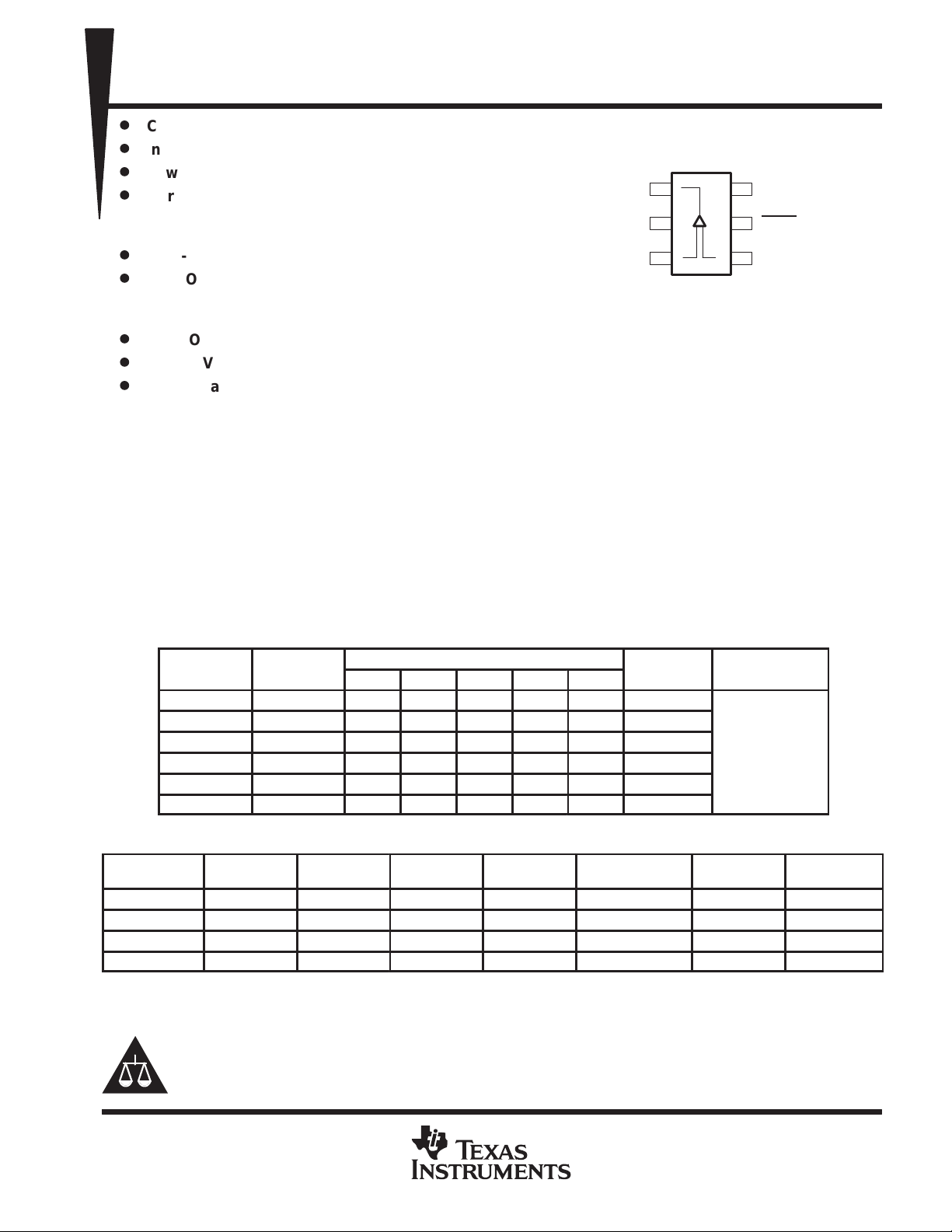
TLV2470
DBV PACKAGE
(TOP VIEW)
1
6
2
5
3
4
V
DD
SHDN
IN–
– ±10 mA at 180 mV
– ±35 mA at 500 mV
D
Input Offset Voltage . . . 250 µV (typ)
D
Supply Voltage Range . . . 2.7 V to 6 V
D
Ultra Small Packaging
– 5 or 6 Pin SOT-23 (TLV2470/1)
– 8 or 10 Pin MSOP (TLV2472/3)
description
The TLV247x is a family of CMOS rail-to-rail input/output operational amplifiers that establishes a new
performance point for supply current versus ac performance. These devices consume just 600 µA/channel
while offering 2.8 MHz of gain-bandwidth product. Along with increased ac performance, the amplifier provides
high output drive capability, solving a major shortcoming of older micropower operational amplifiers. The
TL V247x can swing to within 180 mV of each supply rail while driving a 10-mA load. For non-RRO applications,
the TL V247x can supply ±35 mA at 500 mV off the rail. Both the inputs and outputs swing rail-to-rail for increased
dynamic range in low-voltage applications. This performance makes the TLV247x family ideal for sensor
interface, portable medical equipment, and other data acquisition circuits.
FAMILY PACKAGE TABLE
NUMBER OF
CHANNELS
TLV2470 1 8 8 6 — — Yes
TLV2471 1 8 8 5 — — —
TLV2472 2 8 8 — — 8 —
TLV2473 2 14 14 — — 10 Yes
TLV2474 4 14 14 — 14 — —
TLV2475 4 16 16 — 16 — Yes
PDIP SOIC SOT-23 TSSOP MSOP
PACKAGE TYPES
UNIVERSAL EVM
BOARD
Refer to the EVM
on Guide
Lit# SLOU060
A SELECTION OF SINGLE-SUPPLY OPERATIONAL AMPLIFIER PRODUCTS
V
DEVICE
TLV247X 2.7 – 6.0 250 2.8 1.5 600 ±35 mA I/O
TLV245X 2.7 – 6.0 20 0.22 0.11 23 ±10 mA I/O
TLV246X 2.7 – 6.0 150 6.4 1.6 550 ±90 mA I/O
TLV277X 2.5 – 6.0 360 5.1 10.5 1000 ±10 mA O
†
All specifications measured at 5 V .
Please be aware that an important notice concerning availability, standard warranty, and use in critical applications of
Texas Instruments semiconductor products and disclaimers thereto appears at the end of this data sheet.
PRODUCTION DATA information is current as of publication date.
Products conform to specifications per the terms of Texas Instruments
standard warranty. Production processing does not necessarily include
testing of all parameters.
DD
(V)
V
IO
(µV)
POST OFFICE BOX 655303 • DALLAS, TEXAS 75265
BW
(MHz)
SLEW RATE
(V/µs)
IDD (per channel)
(µA)
Copyright 2000, Texas Instruments Incorporated
†
OUTPUT
DRIVE
RAIL-TO-RAIL
1
TLV2470, TLV2471, TLV2472, TLV2473, TLV2474, TLV2475, TLV247xA
40°C to 125°C
OUTLINE
DIP
DIP
40°C to 125°C
40°C to 125°C
FAMILY OF 600-µA/Ch 2.8-MHz RAIL-TO-RAIL INPUT/OUTPUT
HIGH-DRIVE OPERATIONAL AMPLIFIERS WITH SHUTDOWN
SLOS232B – JUNE 1999 – REVISED MARCH 2000
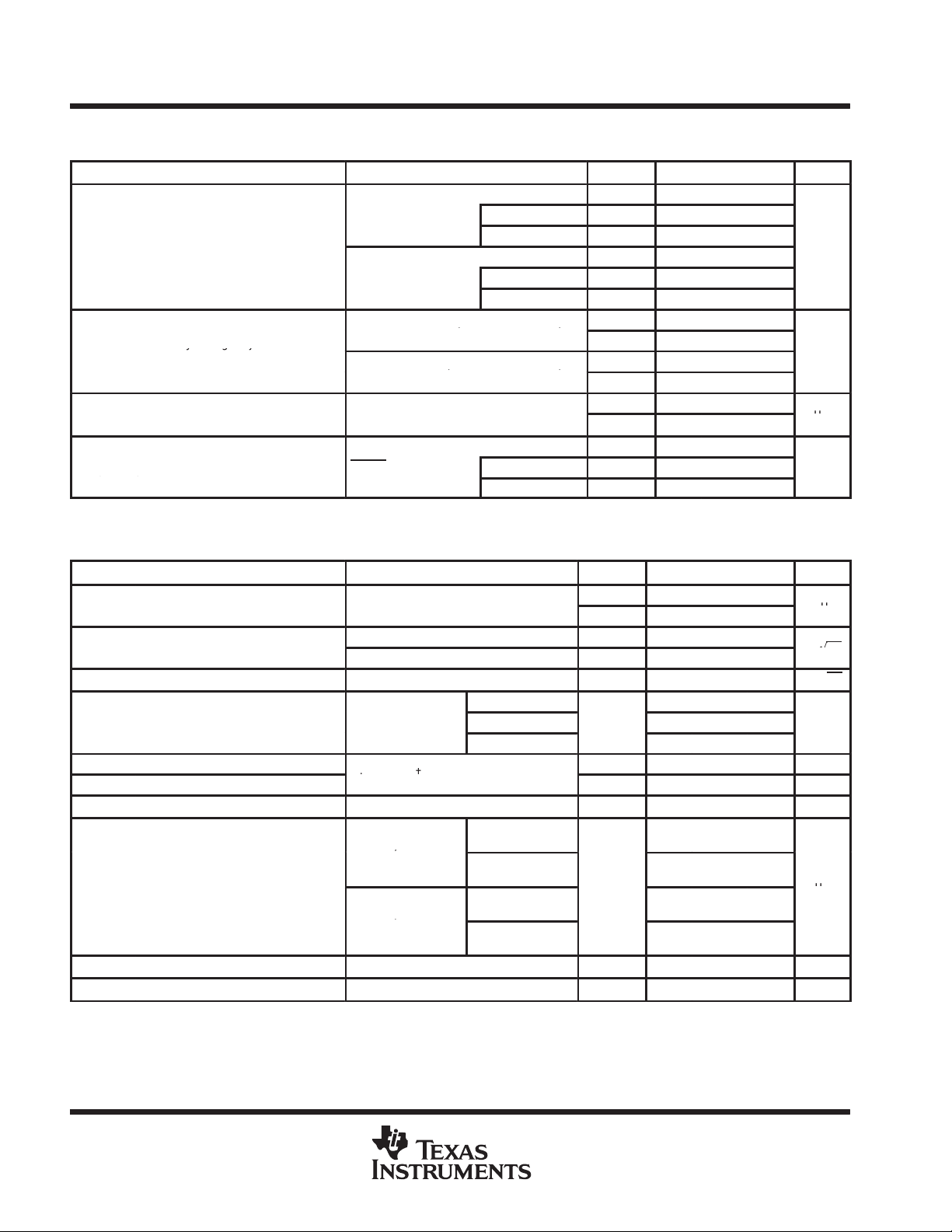
TLV2470 and TLV2471 AVAILABLE OPTIONS
PACKAGED DEVICES
T
A
0°C to 70°C
°
–
†
This package is available taped and reeled. T o order this packaging option, add an R suffix to the part number
(e.g., TLV2470CDR).
T
A
0°C to 70°C
°
–
†
This package is available taped and reeled. To order this packaging option, add an R suffix to the part number (e.g., TLV2472CDR).
‡
xx represents the device date code.
°
SMALL
(D)
TLV2472CD
TLV2473CD
TLV2472ID
TLV2473ID
TLV2472AID
TLV2473AID
SMALL OUTLINE
°
†
†
(D)
TLV2470CD
TLV2471CD
TLV2470ID
TLV2471ID
TLV2470AID
TLV2471AID
TLV2472 AND TLV2473 AV AILABLE OPTIONS
MSOP MSOP
†
(DGN)
TLV2472CDGN—xxTIABU
TLV2472IDGN—xxTIABV
—
—
TLV2470CDBV
TLV2471CDBV
TLV2470IDBV
TLV2471IDBV
SYMBOL
—
—
—
—
SOT-23
†
(DBV)
—
—
PACKAGED DEVICES
‡
(DGQ)
TLV2473CDGQ—xxTIABW—TLV2473CN
TLV2473IDGQ—xxTIABX—TLV2473IN
—
—
—
—
SYMBOL
†
VAUC
VAVC
VAUI
VAVI
—
—
SYMBOL
PLASTIC DIP
‡
—
—
(P)
TLV2470CP
TLV2471CP
TLV2470IP
TLV2471IP
TLV2470AIP
TLV2471AIP
PLASTIC
(N)
—
TLV2473AIN
PLASTIC
(P)
TLV2472CP
—
TLV2472IP
—
TLV2472AIP
—
TLV2474 and TLV2475 AVAILABLE OPTIONS
PACKAGED DEVICES
T
A
0°C to 70°C
°
–
†
This package is available taped and reeled. To order this packaging option, add an R
suffix to the part number (e.g., TL V2474CDR).
°
SMALL OUTLINE
†
(D)
TLV2474CD
TLV2475CD
TLV2474ID
TLV2475ID
TLV2474AID
TLV2475AID
PLASTIC DIP
(N)
TLV2474CN
TLV2475CN
TLV2474IN
TLV2475IN
TLV2474AIN
TLV2475AIN
TSSOP
†
(PWP)
TLV2474CPWP
TLV2475CPWP
TLV2474IPWP
TLV2475IPWP
TLV2474AIPWP
TLV2475AIPWP
2
POST OFFICE BOX 655303 • DALLAS, TEXAS 75265
TLV2470, TLV2471, TLV2472, TLV2473, TLV2474, TLV2475, TLV247xA
FAMILY OF 600-µA/Ch 2.8-MHz RAIL-TO-RAIL INPUT/OUTPUT
HIGH-DRIVE OPERATIONAL AMPLIFIERS WITH SHUTDOWN
SLOS232B – JUNE 1999 – REVISED MARCH 2000
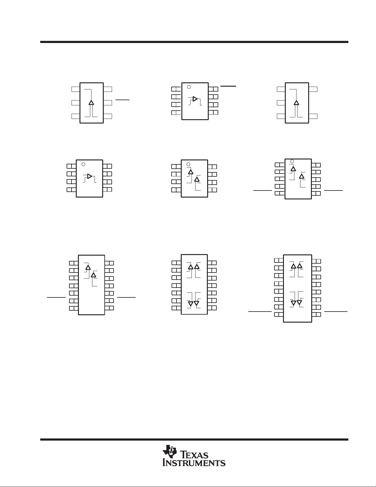
TLV247x PACKAGE PINOUTS
OUT
GND
IN+
D OR P PACKAGE
NC
IN–
IN+
GND
D OR N PACKAGE
TLV2470
DBV PACKAGE
(TOP VIEW)
6
1
2
5
3
4
TLV2471
(TOP VIEW)
1
2
3
4
(TOP VIEW)
8
7
6
5
TLV2473
V
DD
SHDN
IN–
NC
V
DD
OUT
NC
TLV2470
D OR P PACKAGE
(TOP VIEW)
NC
IN–
IN+
GND
D, DGN, OR P PACKAGE
1OUT
1IN–
1IN+
GND
D, N, OR PWP PACKAGE
1
2
3
4
TLV2472
(TOP VIEW)
1
2
3
4
TLV2474
(TOP VIEW)
TLV2471
DBV PACKAGE
(TOP VIEW)
SHDN
8
V
7
6
5
8
7
6
5
DD
OUT
NC
V
DD
2OUT
2IN–
2IN+
OUT
GND
IN+
1OUT
1IN–
1IN+
GND
1SHDN
D, N, OR PWP PACKAGE
1
2
3
TLV2473
DGQ PACKAGE
(TOP VIEW)
1
2
3
4
5
TLV2475
(TOP VIEW)
5
4
10
V
DD
IN–
V
DD
2OUT
9
2IN–
8
2IN+
7
2SHDN
6
1OUT
1IN–
1IN+
GND
NC
1SHDN
NC
NC – No internal connection
1
14
2
13
3
12
4
11
5
10
6
7
1
V
DD
2OUT
2IN–
2IN+
NC
2SHDN
9
8
NC
1OUT
1IN–
1IN+
V
DD
2IN+
2IN–
2OUT
14
4OUT
2
13
4IN–
3
12
4IN+
4
11
GND
5
10
3IN+
6
7
9
3IN–
8
3OUT
1OUT
1IN–
1IN+
V
DD
2IN+
2IN–
2OUT
1/2SHDN
1
2
3
4
5
6
7
8
16
15
14
13
12
11
10
9
description (continued)
Three members of the family (TLV2470/3/5) offer a shutdown terminal for conserving battery life in portable
applications. During shutdown, the outputs are placed in a high-impedance state and the amplifier consumes
only 350 nA/channel. The family is fully specified at 3 V and 5 V across an expanded industrial temperature
range (–40°C to 125°C). The singles and duals are available in the SOT23 and MSOP packages, while the
quads are available in TSSOP . The TL V2470 offers an amplifier with shutdown functionality all in a 6-pin SOT23
package, making it perfect for high density power-sensitive circuits.
4OUT
4IN–
4IN+
GND
3IN+
3IN–
3OUT
3/4SHDN
POST OFFICE BOX 655303 • DALLAS, TEXAS 75265
3
TLV2470, TLV2471, TLV2472, TLV2473, TLV2474, TLV2475, TLV247xA
Suppl
oltage, V
V
Operating free-air temperature, T
°C
Shutdown on/off voltage level
‡
V
FAMILY OF 600-µA/Ch 2.8-MHz RAIL-TO-RAIL INPUT/OUTPUT
HIGH-DRIVE OPERATIONAL AMPLIFIERS WITH SHUTDOWN
SLOS232B – JUNE 1999 – REVISED MARCH 2000
absolute maximum ratings over operating free-air temperature range (unless otherwise noted)
Supply voltage, VDD (see Note 1) 7 V. . . . . . . . . . . . . . . . . . . . . . . . . . . . . . . . . . . . . . . . . . . . . . . . . . . . . . . . . . . . .
Differential input voltage, VID ±V
Continuous total power dissipation See Dissipation Rating Table. . . . . . . . . . . . . . . . . . . . . . . . . . . . . . . . . . . . .
Operating free-air temperature range, T
Maximum junction temperature, TJ 150°C. . . . . . . . . . . . . . . . . . . . . . . . . . . . . . . . . . . . . . . . . . . . . . . . . . . . . . . . .
Storage temperature range, T
Lead temperature 1,6 mm (1/16 inch) from case for 10 seconds 260°C. . . . . . . . . . . . . . . . . . . . . . . . . . . . . . .
†
Stresses beyond those listed under “absolute maximum ratings” may cause permanent damage to the device. These are stress ratings only, and
functional operation of the device at these or any other conditions beyond those indicated under “recommended operating conditions” is not
implied. Exposure to absolute-maximum-rated conditions for extended periods may affect device reliability.
NOTE: All voltage values, except differential voltages, are with respect to GND.
PACKAGE
D (8) 38.3 176 710 mW
D (14) 26.9 122.3 1022 mW
D (16) 25.7 114.7 1090 mW
DBV (5) 55 324.1 385 mW
DBV (6) 55 294.3 425 mW
DGN (8) 4.7 52.7 2.37 W
DGQ (10) 4.7 52.3 2.39 W
N (14, 16) 32 78 1600 mW
P (8) 41 104 1200 mW
PWP (14) 2.07 30.7 4.07 W
PWP (16) 2.07 29.7 4.21 W
. . . . . . . . . . . . . . . . . . . . . . . . . . . . . . . . . . . . . . . . . . . . . . . . . . . . . . . . . . . . . .
: C suffix 0°C to 70°C. . . . . . . . . . . . . . . . . . . . . . . . . . . . . . . . . . . . . .
A
I suffix –40°C to 125°C. . . . . . . . . . . . . . . . . . . . . . . . . . . . . . . . . . . .
–65°C to 150°C. . . . . . . . . . . . . . . . . . . . . . . . . . . . . . . . . . . . . . . . . . . . . . . . . . .
stg
DISSIPATION RATING TABLE
θ
JC
(°C/W)
θ
JA
(°C/W)
TA ≤ 25°C
POWER RATING
†
DD
recommended operating conditions
pp
y v
Common-mode input voltage range, V
p
‡
Relative to GND
DD
ICR
p
A
MIN MAX UNIT
Single supply 2.7 6
Split supply ±1.35 ±3
–0.2 VDD+0.2 V
C-suffix 0 70
I-suffix –40 125
V
IH
V
IL
2
0.8
°
4
POST OFFICE BOX 655303 • DALLAS, TEXAS 75265

TLV247
VIOInput offset voltage
V
TLV247xA
V
DD
VDD/2
0.4µV/°C
IC
0,
pA
I
mA
VOHHigh-level output voltage
V
VDD/2
V
I
10 mA
I
mA
VOLLow-level output voltage
V
VDD/2
V
I
mA
Sourcing
‡
Outside of rails
‡
IOSShort-circuit output current
mA
Sinking
‡
Outside of rails
‡
A
gg g
V
1 V
R
kΩ
dB
TLV2470, TLV2471, TLV2472, TLV2473, TLV2474, TLV2475, TLV247xA
FAMILY OF 600-µA/Ch 2.8-MHz RAIL-TO-RAIL INPUT/OUTPUT
HIGH-DRIVE OPERATIONAL AMPLIFIERS WITH SHUTDOWN
SLOS232B – JUNE 1999 – REVISED MARCH 2000
electrical characteristics at specified free-air temperature, VDD = 3 V (unless otherwise noted)
PARAMETER TEST CONDITIONS
x
p
α
VIO
I
IO
I
IB
I
O
VD
r
i(d)
C
IC
z
o
†
Full range is 0°C to 70°C for C suffix and –40°C to 125°C for I suffix. If not specified, full range is –40°C to 125°C.
‡
Depending on package dissipation rating
Temperature coefficient of input
offset voltage
Input offset current
Input bias current
p
p
p
Output current VO = 0.5 V from rail 25°C ±22 mA
Large-signal differential voltage
amplification
Differential input resistance 25°C 10
Common-mode input
capacitance
Closed-loop output impedance f = 10 kHz, AV = 10 25°C 2
=
V
= 0,
VO = 0,
RS = 50 Ω
=
IC
=
IC
Sourcing,
Sinking,
,
=
O(PP)
f = 10 kHz 25°C 19.3 pF
TLV247xC Full range 100
TLV247xI Full range 300
TLV247xC Full range 100
TLV247xI Full range 300
= –2.5
OH
= –
OH
= 2.5
OL
= 10
OL
TLV247xC Full range 60
TLV247xI Full range 59
TLV247xC Full range 60
TLV247xI Full range 59
= 10
L
†
T
A
25°C 250 2200
Full range 2400
25°C 250 1600
Full range 1800
25°C 1.5 50
25°C 2 50
25°C 2.85 2.94
Full range 2.8
25°C 2.6 2.74
Full range 2.5
25°C 0.07 0.15
Full range 0.2
25°C 0.2 0.35
Full range 0.4
25°C 30
Full range 20
25°C 62
25°C 30
Full range 20
25°C 62
25°C 90 116
Full range 88
MIN TYP MAX
12
UNIT
µ
p
Ω
Ω
°
POST OFFICE BOX 655303 • DALLAS, TEXAS 75265
5
TLV2470, TLV2471, TLV2472, TLV2473, TLV2474, TLV2475, TLV247xA
R
S
50 Ω
CMRR
Common-mode rejection ratio
dB
V
IC
DD
,
IC DD
,
k
ygj
dB
DD
,
IC DD
,
IDDSupply current (per channel)
V
No load
A
Su ly current in shutdown
()
SR
Slew rate at unity gain
O(PP)
,
L
,
V/µs
VnEquivalent input noise voltage
V/√H
V
O(PP)
R
OPEN
‡
V
,
tsSettling time
25°C
s
V
,
FAMILY OF 600-µA/Ch 2.8-MHz RAIL-TO-RAIL INPUT/OUTPUT
HIGH-DRIVE OPERATIONAL AMPLIFIERS WITH SHUTDOWN
SLOS232B – JUNE 1999 – REVISED MARCH 2000
electrical characteristics at specified free-air temperature, VDD = 3 V (unless otherwise noted)
(continued)
PARAMETER TEST CONDITIONS
VIC = 0 to 3 V,
=
=–
= 0.2 to 3.2 V,
RS = 50 Ω,
Outside of rails
V
= 2.7 V to 6 V, V
SVR
I
DD(SHDN)
†
Full range is 0°C to 70°C for C suffix and –40°C to 125°C for I suffix. If not specified, full range is –40°C to 125°C.
Supply voltage rejection ratio
(∆VDD /∆VIO)
pp
pp
mode (TLV2470, TLV2473,
TLV2475) (per channel)
p
No load
= 3 V to 5 V, V
V
No load
= 1.5 V,
O
SHDN = 0 V
TLV247xC Full range 59
TLV247xI Full range 58
TLV247xC Full range 60
TLV247xI Full range 59
= V
/2,
= V
/2,
TLV247xC Full range 2000
TLV247xI Full range 4000
†
T
A
25°C 61 78
25°C 62 78
25°C 74 90
Full range 66
25°C 77 92
Full range 68
25°C 550 750
Full range 800
25°C 350 1500
MIN TYP MAX
UNIT
µ
nA
operating characteristics at specified free-air temperature, VDD = 3 V (unless otherwise noted)
PARAMETER TEST CONDITIONS
V
= 0.8 V, C
RL = 10 kΩ
p
I
n
THD + N Total harmonic distortion plus noise
t
(on)
t
(off)
φ
m
†
Full range is 0°C to 70°C for C suffix and –40°C to 125°C for I suffix. If not specified, full range is –40°C to 125°C.
‡
Depending on package dissipation rating
Equivalent input noise current f = 1 kHz 25°C 0.405
Amplifier turnon time
Amplifier turnoff time
Gain-bandwidth product
Phase margin
Gain margin
f = 100 Hz 25°C 28
f = 1 kHz 25°C 15
=
= 2 V,
RL = 10 kΩ,
f = 1 kHz
=
L
f = 10 kHz, RL = 600 Ω
V
(STEP)PP
A
= –1,
CL = 10 pF,
RL = 10 kΩ
V
(STEP)PP
= –1,
A
CL = 56 pF,
RL = 10 kΩ
RL = 10 kΩ, CL = 1000 pF
RL = 10 kΩ, CL = 1000 pF
= 2 V,
= 2 V,
= 150 pF,
AV = 1 0.02%
AV = 10
AV = 100 0.5%
0.1% 1.5
0.01%
0.1%
0.01% 4
†
T
A
25°C
Full range 0.6
25°C
25°C 5 µs
25°C 250 ns
25°C 2.8 MHz
°
25°C 61°
25°C 15 dB
MIN TYP MAX UNIT
1.1 1.4
0.1%
3.9
1.6
n
pA/√Hz
µ
z
6
POST OFFICE BOX 655303 • DALLAS, TEXAS 75265
TLV247
VIOInput offset voltage
V
TLV247xA
V
VDD/
0.4µV/°C
V
V
R
S
Ω
pA
I
mA
VOHHigh-level output voltage
V
VDD/2
V
I
10 mA
I
mA
VOLLow-level output voltage
V
VDD/2
V
I
mA
Sourcing
‡
Outside of rails
‡
IOSShort-circuit output current
mA
Sinking
‡
Outside of rails
‡
A
gg g
V
3 V
R
kΩ
dB
TLV2470, TLV2471, TLV2472, TLV2473, TLV2474, TLV2475, TLV247xA
FAMILY OF 600-µA/Ch 2.8-MHz RAIL-TO-RAIL INPUT/OUTPUT
HIGH-DRIVE OPERATIONAL AMPLIFIERS WITH SHUTDOWN
SLOS232B – JUNE 1999 – REVISED MARCH 2000
electrical characteristics at specified free-air temperature, VDD = 5 V (unless otherwise noted)
PARAMETER TEST CONDITIONS
x
p
α
VIO
I
IO
I
IB
I
O
VD
r
i(d)
C
IC
z
o
†
Full range is 0°C to 70°C for C suffix and –40°C to 125°C for I suffix. If not specified, full range is –40°C to 125°C.
‡
Depending on package dissipation rating
Temperature coefficient of input
offset voltage
Input offset current
Input bias current
p
p
p
Output current VO = 0.5 V from rail 25°C ±35 mA
Large-signal differential voltage
amplification
Differential input resistance 25°C 10
Common-mode input
capacitance
Closed-loop output impedance f = 10 kHz, AV = 10 25°C 1.8
=
=
O
2
= 0,
,
TLV247xC Full range 100
TLV247xI Full range 300
TLV247xC Full range 100
TLV247xI Full range 300
= –2.5
OH
= –
OH
= 2.5
OL
= 10
OL
TLV247xC Full range 61
TLV247xI Full range 58
TLV247xC Full range 61
TLV247xI Full range 58
= 10
L
DD
= 0,
IC
=
= 50
=
IC
=
IC
Sourcing,
Sinking,
O(PP)
f = 10 kHz 25°C 18.9 pF
†
T
A
25°C 250 2200
Full range 2400
25°C 250 1600
Full range 2000
25°C 1.7 50
25°C 2.5 50
25°C 4.85 4.96
Full range 4.8
25°C 4.72 4.82
Full range 4.65
25°C 0.07 0.15
Full range 0.2
25°C 0.178 0.28
Full range 0.35
25°C 90
Full range 60
25°C 63
25°C 110
Full range 60
25°C 63
25°C 92 120
Full range 91
MIN TYP MAX
12
UNIT
µ
p
Ω
Ω
°
POST OFFICE BOX 655303 • DALLAS, TEXAS 75265
7
TLV2470, TLV2471, TLV2472, TLV2473, TLV2474, TLV2475, TLV247xA
R
S
50 Ω
CMRR
Common-mode rejection ratio
dB
V
IC
DD
,
IC DD
,
k
ygj
dB
DD
,
IC DD
,
IDDSupply current (per channel)
V
No load
A
Su ly current in shutdown
nA
()
SR
Slew rate at unity gain
O(PP)
,
L
,
V/µs
VnEquivalent input noise voltage
V/√H
V
O(PP)
R
OPEN
‡
V
,
tsSettling time
25°C
s
V
,
FAMILY OF 600-µA/Ch 2.8-MHz RAIL-TO-RAIL INPUT/OUTPUT
HIGH-DRIVE OPERATIONAL AMPLIFIERS WITH SHUTDOWN
SLOS232B – JUNE 1999 – REVISED MARCH 2000
electrical characteristics at specified free-air temperature, VDD = 5 V (unless otherwise noted)
(continued)
PARAMETER TEST CONDITIONS
VIC = 0 to 5 V,
=
=–
= 0.2 to 5.2 V,
RS = 50 Ω,
Outside of rails
V
= 2.7 V to 6 V, V
SVR
I
DD(SHDN)
†
Full range is 0°C to 70°C for C suffix and –40°C to 125°C for I suffix. If not specified, full range is –40°C to 125°C.
Supply voltage rejection ratio
(∆VDD /∆VIO)
pp
pp
mode (TLV2470, TLV2473,
TLV2475) (per channel)
p
No load
= 3 V to 5 V, V
V
No load
= 2.5 V,
O
SHDN = 0 V
TLV247xC Full range 63
TLV247xI Full range 58
TLV247xC Full range 61
TLV247xI Full range 58
= V
/2,
= V
/2,
TLV247xC Full range 3000
TLV247xI Full range 6000 nA
†
T
A
25°C 64 84
25°C 63 82
25°C 74 90
Full range 66
25°C 77 92
Full range 66
25°C 600 900
Full range 1000
25°C 1000 2500
MIN TYP MAX
UNIT
µ
operating characteristics at specified free-air temperature, VDD = 5 V (unless otherwise noted)
PARAMETER TEST CONDITIONS
V
= 2 V, C
RL = 10 kΩ
p
I
n
THD + N Total harmonic distortion plus noise
t
(on)
t
(off)
φ
m
†
Full range is 0°C to 70°C for C suffix and –40°C to 125°C for I suffix. If not specified, full range is –40°C to 125°C.
‡
Disable and enable time are defined as the interval between application of logic signal to SHDN and the point at which the supply current has
reached half its final value.
Equivalent input noise current f = 1 kHz 25°C 0.39
Amplifier turnon time
Amplifier turnoff time
Gain-bandwidth product
Phase margin
Gain margin
f = 100 Hz 25°C 28
f = 1 kHz 25°C 15
=
= 4 V,
RL = 10 kΩ,
f = 1 kHz
=
L
f = 10 kHz, RL = 600 Ω
V
(STEP)PP
A
= –1,
CL = 10 pF,
RL = 10 kΩ
V
(STEP)PP
= –1,
A
CL = 56 pF,
RL = 10 kΩ
RL = 10 kΩ, CL = 1000 pF
RL = 10 kΩ, CL = 1000 pF
= 2 V,
= 2 V,
= 150 pF,
AV = 1 0.01%
AV = 10
AV = 100 0.3%
0.1% 1.8
0.01%
0.1%
0.01% 3
†
T
A
25°C
Full range 0.7
25°C
25°C 5 µs
25°C 250 ns
25°C 2.8 MHz
°
25°C 68°
25°C 23 dB
MIN TYP MAX UNIT
1.1 1.5
0.05%
3.3
1.7
n
pA/√Hz
µ
z
8
POST OFFICE BOX 655303 • DALLAS, TEXAS 75265
Free-air temperature
3, 4
SR
Slew rate
TLV2470, TLV2471, TLV2472, TLV2473, TLV2474, TLV2475, TLV247xA
FAMILY OF 600-µA/Ch 2.8-MHz RAIL-TO-RAIL INPUT/OUTPUT
HIGH-DRIVE OPERATIONAL AMPLIFIERS WITH SHUTDOWN
SLOS232B – JUNE 1999 – REVISED MARCH 2000
TYPICAL CHARACTERISTICS
Table of Graphs
FIGURE
V
IO
I
IB
I
IO
V
OH
V
OL
Z
o
I
DD
PSRR Power supply rejection ratio vs Frequency 11
CMRR Common-mode rejection ratio vs Frequency 12
V
n
V
O(PP)
A
VD
φ
m
THD+N Total harmonic distortion + noise vs Frequency 27, 28
V
O
I
DD(SHDN)
I
DD(SHDN)
I
DD(SHDN)
Input offset voltage vs Common-mode input voltage 1, 2
Input bias current
Input offset current
High-level output voltage vs High-level output current 5, 7
Low-level output voltage vs Low-level output current 6, 8
Output impedance vs Frequency 9
Supply current vs Supply voltage 10
Equivalent input noise voltage vs Frequency 13
Maximum peak-to-peak output voltage vs Frequency 14, 15
Differential voltage gain and phase vs Frequency 16, 17
Phase margin vs Load capacitance 18, 19
Gain margin vs Load capacitance 20, 21
Gain-bandwidth product vs Supply voltage 22
Crosstalk vs Frequency 26
Large and small signal follower vs Time 29 – 32
Shutdown pulse response vs Time 33, 34
Shutdown forward and reverse isolation vs Frequency 35, 36
Shutdown supply current vs Supply voltage 37
Shutdown supply current vs Free-air temperature 38
Shutdown pulse current vs Time 39, 40
vs
vs Supply voltage 23
vs Free-air temperature 24, 25
p
POST OFFICE BOX 655303 • DALLAS, TEXAS 75265
9
TLV2470, TLV2471, TLV2472, TLV2473, TLV2474, TLV2475, TLV247xA
FAMILY OF 600-µA/Ch 2.8-MHz RAIL-TO-RAIL INPUT/OUTPUT
HIGH-DRIVE OPERATIONAL AMPLIFIERS WITH SHUTDOWN
SLOS232B – JUNE 1999 – REVISED MARCH 2000
TYPICAL CHARACTERISTICS
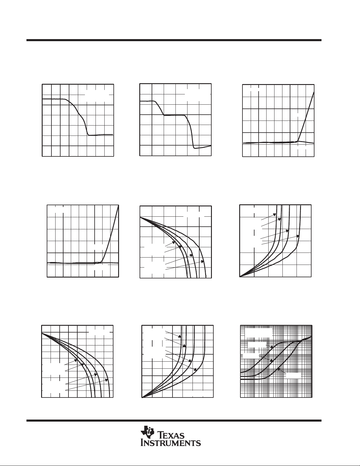
INPUT OFFSET VOLTAGE
vs
COMMON-MODE INPUT VOLTAGE
600
400
200
0
–200
–400
Input Offset Voltage ––Vµ
IO
V
–600
–800
–0.5 0.0 0.5 1.0 1.5 2.0 2.5 3.0 3.5
V
– Common-Mode Input Voltage – V
ICR
VDD=3 V
TA=25° C
Figure 1
INPUT BIAS AND INPUT OFFSET
CURRENTS
vs
FREE-AIR TEMPERATURE
50
VDD=5 V
40
30
20
10
– Input Bias Current – pA
– Input Offset Current – pA
IB
IO
0
I
I
–10
–55 –35 –15 5 25 45 65 85 105 125
TA – Free-Air Temperature – °C
Figure 4
INPUT OFFSET VOLTAGE
vs
COMMON-MODE INPUT VOLTAGE
600
400
200
0
–200
–400
Input Offset Voltage ––Vµ
IO
–600
V
–800
–0.5 0.5 1.5 2.5 3.5 4.5 5.5
V
– Common-Mode Input Voltage – V
ICR
VDD=5 V
TA=25 °C
Figure 2
HIGH-LEVEL OUTPUT VOLTAGE
vs
HIGH-LEVEL OUTPUT CURRENT
3.5
3.0
2.5
2.0
TA=125°C
I
IB
I
IO
1.5
TA=85°C
1.0
– High-Level Output Voltage – V
OH
V
TA=25°C
0.5
TA=–40°C
0
0 102030405060
IOH – High-Level Output Current – mA
VDD=3 V
Figure 5
INPUT BIAS AND INPUT OFFSET
CURRENTS
vs
FREE-AIR TEMPERATURE
50
VDD=3 V
40
30
20
10
– Input Bias Current – pA
– Input Offset Current – pA
IB
IO
0
I
I
–10
–55 –35 –15 5 25 45 65 85 105 125
TA – Free-Air Temperature – °C
Figure 3
LOW-LEVEL OUTPUT VOLTAGE
vs
LOW-LEVEL OUTPUT CURRENT
3.0
VDD=3 V
2.5
TA=125°C
TA=85°C
2.0
TA=25°C
1.5
TA=–40°C
1.0
0.5
OL
V – Low-Level Output Voltage – V
0
0 1020304050
IOL – Low-Level Output Current – mA
Figure 6
I
IB
I
IO
HIGH-LEVEL OUTPUT VOLTAGE
vs
HIGH-LEVEL OUTPUT CURRENT
5.5
5.0
4.5
4.0
3.5
3.0
2.5
TA=125°C
2.0
TA=85°C
1.5
– High-Level Output Voltage – V
TA=25°C
1.0
OH
TA=–40°C
0.5
V
0
0 20 40 60 80 100 120 140 160
IOH – High-Level Output Current – mA
Figure 7
10
VDD=5 V
LOW-LEVEL OUTPUT VOLTAGE
vs
LOW-LEVEL OUTPUT CURRENT
5.0
TA=125°C
4.5
TA=85°C
4.0
3.5
TA=25°C
3.0
TA=–40°C
2.5
2.0
1.5
1.0
OL
V – Low-Level Output Voltage – V
0.5
0
0 20 40 60 80 100 120 140
IOL – Low-Level Output Current – mA
VDD=5 V
Figure 8
POST OFFICE BOX 655303 • DALLAS, TEXAS 75265
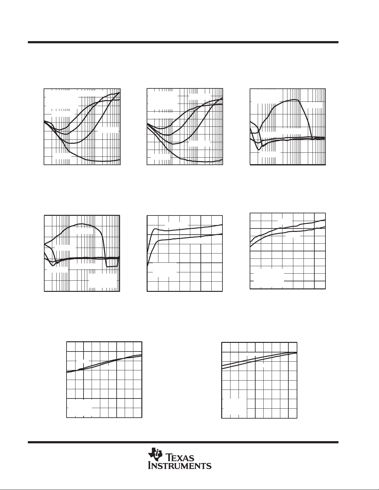
OUTPUT IMPEDANCE
vs
FREQUENCY
1000
VDD=3 & 5 V
Ω
– Output Impedance –Z
TA=25°C
o
0.01
100
0.1
AV=100
10
AV=10
1
AV=1
100 1k 10k 100k 1M 10M
f – Frequency – Hz
Figure 9

TLV2470, TLV2471, TLV2472, TLV2473, TLV2474, TLV2475, TLV247xA
FAMILY OF 600-µA/Ch 2.8-MHz RAIL-TO-RAIL INPUT/OUTPUT
HIGH-DRIVE OPERATIONAL AMPLIFIERS WITH SHUTDOWN
SLOS232B – JUNE 1999 – REVISED MARCH 2000
TYPICAL CHARACTERISTICS
SUPPLY CURRENT
vs
SUPPLY VOLTAGE
1.0
0.9
TA=85°C
0.8
0.7
0.6
0.5
0.4
– Supply Current – mA
0.3
0.2
DD
AV= 1
I
SHDN= V
0.1
0
2.5 3.0 3.5 4.0 4.5 5.0 5.5 6.0
DD
Per Channel
VDD – Supply Voltage – V
TA=125°C
TA=25°C
TA=–40°C
Figure 10
EQUIVALENT NOISE VOLTAGE
vs
FREQUENCY
80
70
nV/ Hz– Equivalent Input Noise Voltage –V
60
50
40
30
20
10
0
n
VDD=3 & 5 V
AV= 10
VIN= VDD/2
TA=25°C
1k 10k 100k10 100
f – Frequency – Hz
Figure 13
DIFFERENTIAL VOLTAGE GAIN AND PHASE
FREQUENCY
100
80
60
40
20
0
– Differential Voltage Gain – dB
–20
VD
A
–40
100 1k 10k 100k
Frequency – Hz
Figure 16
vs
VDD=±3
RL=600 Ω
CL=0
TA=25°C
1M 10M 100M
POWER SUPPLY REJECTION RATIO
vs
FREQUENCY
100
90
80
70
60
50
– Power Supply Rejection Ratio – dBPSRR
40
30
10 100 1k 10k 100k 1M 10M
PSRR+
PSRR–
f – Frequency – Hz
VDD=3 & 5 V
RF=5 kΩ
RI=50 Ω
TA=25°C
Figure 11 Figure 12
MAXIMUM PEAK-TO-PEAK
OUTPUT VOLTAGE
vs
V
V
O(PP)
O(PP)
FREQUENCY
=5 V
=3 V
f – Frequency – Hz
Figure 14
THD+N ≤ 2.0%
RL=10 kΩ
TA=25°C
5.5
5.0
4.5
4.0
3.5
3.0
2.5
2.0
1.5
1.0
0.5
– Maximum Peak-To-Peak Output Voltage – V
0
O(PP)
V
DIFFERENTIAL VOLTAGE GAIN AND PHASE
45
0
–45
–90
–135
Phase – °
–180
–225
–270
1M10k 100k
100
80
60
40
20
0
– Differential Voltage Gain – dBA
–20
VD
–40
100 1k 10k 100k
COMMON-MODE REJECTION RATIO
vs
FREQUENCY
130
120
110
100
90
80
VDD=3 V
70
VIC=1.5 V
60
50
CMRR – Common-Mode Rejection Ratio – dB
100 1k 10k 100k 1M 10M
VDD=5 V
VIC=2.5 V
f – Frequency – Hz
MAXIMUM PEAK-TO-PEAK
OUTPUT VOLTAGE
vs
V
=5 V
O(PP)
V
=3 V
O(PP)
f – Frequency – Hz
FREQUENCY
THD+N ≤ 2.0%
RL=600 Ω
TA=25°C
5.5
5.0
4.5
4.0
3.5
3.0
2.5
2.0
1.5
1.0
0.5
– Maximum Peak-To-Peak Output Voltage – V
0
O(PP)
V
Figure 15
vs
FREQUENCY
45
VDD=±5
RL=600 Ω
CL=0
TA=25°C
Frequency – Hz
1M 10M 100M
0
–45
–90
–135
–180
–225
–270
Phase – °
Figure 17
1M10k 100k
POST OFFICE BOX 655303 • DALLAS, TEXAS 75265
11
TLV2470, TLV2471, TLV2472, TLV2473, TLV2474, TLV2475, TLV247xA
FAMILY OF 600-µA/Ch 2.8-MHz RAIL-TO-RAIL INPUT/OUTPUT
HIGH-DRIVE OPERATIONAL AMPLIFIERS WITH SHUTDOWN
SLOS232B – JUNE 1999 – REVISED MARCH 2000
TYPICAL CHARACTERISTICS
PHASE MARGIN
vs
LOAD CAPACITANCE
90
VDD=3 V
80
RL=10 kΩ
TA=25°C
See Figure 42
70
Rnull=100
60
50
40
– Phase Margin – °
30
m
φ
20
10
Rnull=0
0
100 1k 10k 100k
CL – Load Capacitance – pF
Rnull=50
Figure 18
GAIN MARGIN
vs
LOAD CAPACITANCE
0
5
10
15
20
Gain Margin – dB
25
30
35
Rnull=20
Rnull=50
100 1k 10k 100k
CL – Load Capacitance – pF
Rnull=0
Rnull=100
VDD=5V
RL=10 kΩ
TA=25°C
Figure 21
SLEW RATE
FREE-AIR TEMPERATURE
Rnull=20
vs
PHASE MARGIN
vs
LOAD CAPACITANCE
100
VDD=5V
90
RL=10 kΩ
TA=25°C
80
See Figure 42
70
Rnull=100
60
50
40
– Phase Margin – °
30
m
φ
20
10
Rnull=0
0
100 1k 10k 100k
CL – Load Capacitance – pF
Rnull=50
Rnull=20
Figure 19
GAIN-BANDWIDTH PRODUCT
vs
SUPPLY VOLTAGE
4.0
3.5
3.0
2.5
2.0
1.5
1.0
Gain-Bandwidth Product – MHz
0.5
0
2.5 3.0 3.5 4.0 4.5 5.0 5.5 6.0
RL=10 kΩ
RL=600 Ω
CL=11 pF
f=10 kHz
TA=25°C
VDD – Supply Voltage – V
Figure 22
GAIN MARGIN
vs
LOAD CAPACITANCE
0
VDD=3V
RL=10 kΩ
TA=25°C
5
10
15
20
Gain Margin – dB
25
30
Rnull=20
Rnull=50
100 1k 10k 100k
CL – Load Capacitance – pF
Rnull=100
Figure 20
SLEW RATE
vs
SUPPLY VOLTAGE
2.0
1.8
1.6
1.4
1.2
1.0
0.8
0.6
SR – Slew Rate – V/µs
V
O(PP)
0.4
AV=–1
RL=10 kΩ
0.2
CL=150 pF
0
2.5 3.0 3.5 4.0 4.5 5.0 5.5 6.0
SR–
=1.5 V
VDD – Supply Voltage – V
Figure 23
SLEW RATE
vs
FREE-AIR TEMPERATURE
Rnull=0
SR+
12
2.00
1.75
SR – Slew Rate – V/µs
1.50
1.25
1.00
0.75
0.50
0.25
SR+
VDD=3 V
RL=10 kΩ
CL=150 pF
AV=–1
0
–55 –35 –15 5 25 45 65 85 105 125
TA – Free-Air Temperature – °C
SR–
Figure 24
2.00
1.75
1.50
1.25
1.00
0.75
0.50
SR – Slew Rate – V/µs
0.25
0
–55 –35 –15 5 25 45 65 85 105 125
POST OFFICE BOX 655303 • DALLAS, TEXAS 75265
SR–
SR+
VDD=5 V
RL=10 kΩ
CL=150 pF
AV=–1
TA – Free-Air Temperature – °C
Figure 25
TLV2470, TLV2471, TLV2472, TLV2473, TLV2474, TLV2475, TLV247xA
FAMILY OF 600-µA/Ch 2.8-MHz RAIL-TO-RAIL INPUT/OUTPUT
HIGH-DRIVE OPERATIONAL AMPLIFIERS WITH SHUTDOWN
SLOS232B – JUNE 1999 – REVISED MARCH 2000
TYPICAL CHARACTERISTICS
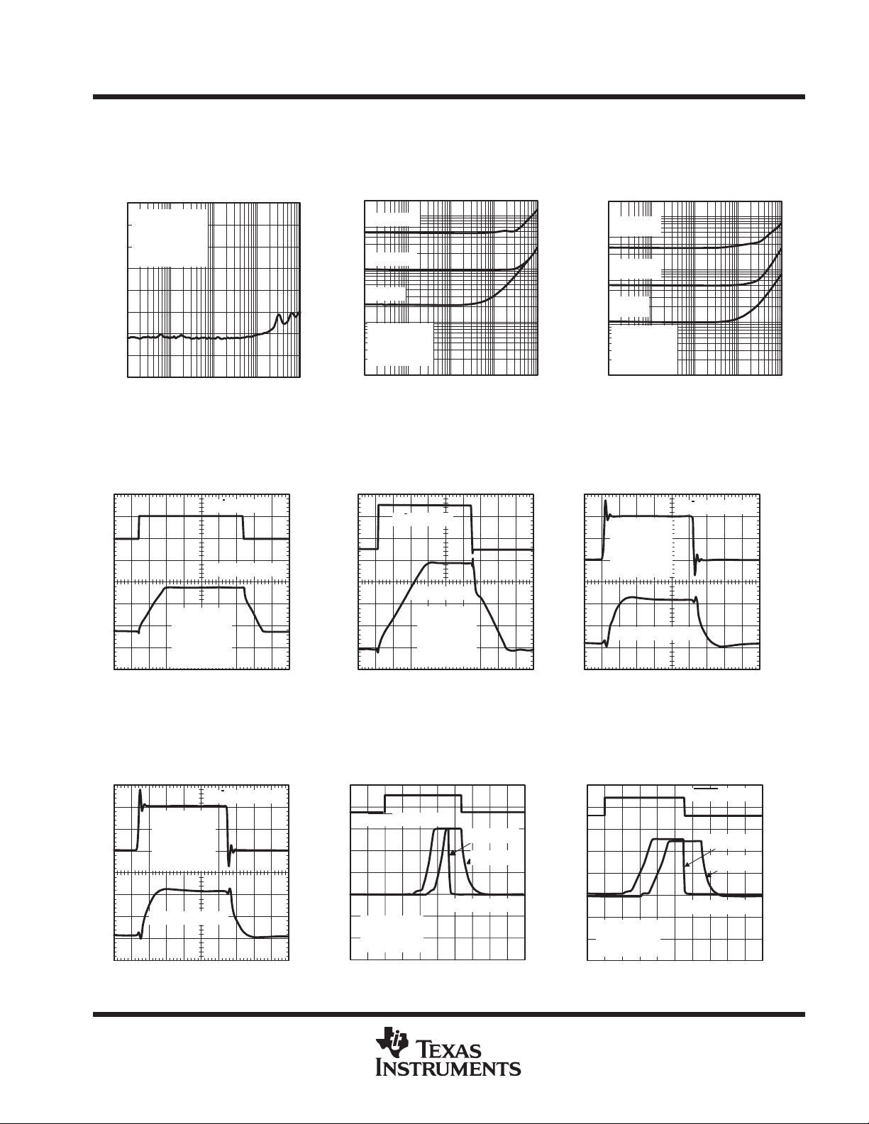
CROSSTALK
vs
=2V
I(PP)
f – Frequency – Hz
FREQUENCY
1 k
0
VDD = 3V & 5V
–20
AV = 1
RL= 600Ω
V
–40
All Channels
–60
–80
–100
Crosstalk – dB
–120
–140
–160
10 100 10 k 100 k
Figure 26
LARGE SIGNAL FOLLOWER
PULSE RESPONSE
vs
TIME
VI (2 V/DIV)
VO (1 V/DIV)
– Output Voltage
O
V
0 12345678910
VDD = 3 V
RL = 10 kΩ
CL = 8 pF
f = 85 kHz
TA = 25°C
t – Time – µs
Figure 29
TOTAL HARMONIC
DISTORTION PLUS NOISE
vs
FREQUENCY
1
AV = 100
AV = 10
0.1
AV = 1
0.01
VDD = 3 V
RL = 10 kΩ
V0 = 2 V
PP
TA = 25°C
THD+N–Total Harmonic Distortion + Noise
0.001
10 1k 10k100
f – Frequency – Hz
Figure 27
LARGE SIGNAL FOLLOWER
PULSE RESPONSE
vs
TIME
VI (2 V/DIV)
VO (1 V/DIV)
– Output Voltage V
O
0 123 45 678910
VDD = 5 V
RL = 10 kΩ
CL = 8 pF
f = 85 kHz
TA = 25°C
t – Time – µs
Figure 30
100k
TOTAL HARMONIC
DISTORTION PLUS NOISE
vs
FREQUENCY
1
AV = 100
AV = 10
0.1
AV = 1
0.01
VDD = 5 V
RL = 10 kΩ
V0 = 4 V
PP
TA = 25°C
THD+N–Total Harmonic Distortion + Noise
0.001
10 1k 10k100
f – Frequency – Hz
Figure 28
SMALL SIGNAL FOLLOWER
PULSE RESPONSE
vs
TIME
VI (50 mV/DIV)
VDD = 3 V
RL = 10 kΩ
CL = 8 pF
f = 1 MHz
TA = 25°C
– Output Voltage V
O
VO (50 mV/DIV)
0 100 200 300 400 500
t – Time – µs
Figure 31
100k
SMALL SIGNAL FOLLOWER
PULSE RESPONSE
vs
TIME
VI (50 mV/DIV)
VDD = 5 V
RL = 10 kΩ
CL = 8 pF
f = 1 MHz
TA = 25°C
– Output Voltage V
O
0 100 200 300 400 500
VO (50 mV/DIV)
t – Time – µs
Figure 32
SHUTDOWN (ON AND OFF)
PULSE RESPONSE
vs
TIME
V
(2 V/DIV)
SHDN
RL = 600 Ω
RL = 10 kΩ
– Output Voltage V
O
VDD = 3 V
CL = 8 pF
TA = 25°C
02468101214
VO (500 mV/DIV)
t – Time – µs
16
Figure 33
POST OFFICE BOX 655303 • DALLAS, TEXAS 75265
SHUTDOWN (ON AND OFF)
PULSE RESPONSE
vs
TIME
V
– Output Voltage V
O
VDD = 5 V
CL = 8 pF
TA = 25°C
02 4 6810121416
t – Time – µs
Figure 34
(2 V/DIV)
SHDN
RL = 600 Ω
RL = 10 kΩ
VO (1 V/DIV)
18
13

TLV2470, TLV2471, TLV2472, TLV2473, TLV2474, TLV2475, TLV247xA
FAMILY OF 600-µA/Ch 2.8-MHz RAIL-TO-RAIL INPUT/OUTPUT
HIGH-DRIVE OPERATIONAL AMPLIFIERS WITH SHUTDOWN
SLOS232B – JUNE 1999 – REVISED MARCH 2000
TYPICAL CHARACTERISTICS
SHUTDOWN FORWARD
ISOLATION
vs
FREQUENCY
120
100
80
60
40
20
Shutdown Forward Isolation - dB
RL=10 kΩ
0
100 1k 10k 100k
VDD = 3 & 5 V
CL=0 pF
AV = 1
V
I(PP)
f – Frequency – Hz
Figure 35
SHUTDOWN PULSE CURRENT
2
1.75
1.5
1.25
0.75
0.5
– Supply Current – mA
0.25
DD
I
–0.25
–0.5
Shutdown Pulse
1
0
IDD RL=10 kΩ
IDD RL=600Ω
0 4 8 121620242830
t – Time – µs
=0.1, 1.5, 3 V
RL=600 Ω
vs
TIME
VDD = 3 V
CL=8 pF
TA=25°C
Figure 39
1M 10M
SHUTDOWN REVERSE ISOLATION
vs
FREQUENCY
120
100
80
60
40
20
Shutdown Forward Isolation - dB
RL=10 kΩ
0
100 1k 10k 100k
VDD = 3 & 5 V
RL=10 kΩ
CL=0 pF
AV = 1
VIN=0.1, 1.5, 3 Vp-p
f – Frequency – Hz
RL=600 Ω
Figure 36
SHUTDOWN SUPPLY CURRENT
vs
FREE-AIR TEMPERATURE
1.6
1.4
1.2
1.0
VDD=5 V
0.8
0.6
0.4
0.2
DD
I Shutdown Supply Current ––Aµ
0
–55 –35 –15 5 25 45 65 85 105 125
SD MODE Channel 1 & 2
AV = 1
RL= OPEN
VIN=V
DD/2
VDD=3 V
TA – Free-Air Temperature – °C
Figure 38
4
3
2
1
0
–1
–2
–3
–4
Shutdown Pulse – V
–5
–6
–7
–8
SHUTDOWN SUPPLY CURRENT
2.0
µA
1.8
1.6
1.4
1.2
1.0
0.8
TA=–40
0.6
– Shutdown Supply Current –
0.4
0.2
DD(SHDN)
0
I
1M 10M
2.5 3.0 3.5 4.0 4.5 5.0 5.5 6.0
SHUTDOWN PULSE CURRENT
TIME
2
1.75
1.5
1.25
1
0.75
0.5
– Supply Current – mA
0.25
DD
I
0
–0.25
–0.5
Shutdown Pulse
IDD RL=10 kΩ
IDD RL=600 Ω
VDD = 5 V
CL=8 pF
TA=25°C
048 3024201612
t – Time – µs
Figure 40
vs
SUPPLY VOLTAGE
TA=125
TA=85
TA=25
VDD – Supply Voltage – V
Figure 37
vs
Shutdown On
RL=OPEN
VI=V
6
4
2
0
–2
–4
–6
–8
–10
–12
28
DD/2
Shutdown Pulse – V
14
POST OFFICE BOX 655303 • DALLAS, TEXAS 75265

TLV2470, TLV2471, TLV2472, TLV2473, TLV2474, TLV2475, TLV247xA
FAMILY OF 600-µA/Ch 2.8-MHz RAIL-TO-RAIL INPUT/OUTPUT
HIGH-DRIVE OPERATIONAL AMPLIFIERS WITH SHUTDOWN
SLOS232B – JUNE 1999 – REVISED MARCH 2000
PARAMETER MEASUREMENT INFORMATION
_
+
R
null
R
L
C
L
Figure 41
APPLICATION INFORMATION
driving a capacitive load
When the amplifier is configured in this manner, capacitive loading directly on the output will decrease the
device’s phase margin leading to high frequency ringing or oscillations. Therefore, for capacitive loads of greater
than 10 pF, it is recommended that a resistor be placed in series (R
shown in Figure 42. A minimum value of 20 Ω should work well for most applications.
R
F
R
Input
G
_
+
R
NULL
C
LOAD
) with the output of the amplifier, as
NULL
Output
Figure 42. Driving a Capacitive Load
offset voltage
The output offset voltage, (VOO) is the sum of the input offset voltage (VIO) and both input bias currents (IIB) times
the corresponding gains. The following schematic and formula can be used to calculate the output offset
voltage:
R
F
I
VOO+
R
G
R
S
V
ǒ
IO
Figure 43. Output Offset Voltage Model
1
) ǒ
IB–
+
V
I
I
IB+
R
F
Ǔ
"
I
Ǔ
IB
R
G
)
–
+
R
1
) ǒ
F
R
G
R
ǒ
S
V
O
Ǔ
"
I
Ǔ
IB–RF
POST OFFICE BOX 655303 • DALLAS, TEXAS 75265
15

TLV2470, TLV2471, TLV2472, TLV2473, TLV2474, TLV2475, TLV247xA
FAMILY OF 600-µA/Ch 2.8-MHz RAIL-TO-RAIL INPUT/OUTPUT
HIGH-DRIVE OPERATIONAL AMPLIFIERS WITH SHUTDOWN
SLOS232B – JUNE 1999 – REVISED MARCH 2000
APPLICATION INFORMATION
general configurations
When receiving low-level signals, limiting the bandwidth of the incoming signals into the system is often
required. The simplest way to accomplish this is to place an RC filter at the noninverting terminal of the amplifier
(see Figure 44).
R
G
R
F
–
C1
R
F
R
G
+
ǒ
Ǔ
1)sR1C1
f
1
–3dB
Ǔ
V
I
R1
V
O
+ ǒ
1
V
I
)
+
V
O
1
2pR1C1
Figure 44. Single-Pole Low-Pass Filter
If even more attenuation is needed, a multiple pole filter is required. The Sallen-Key filter can be used for this
task. For best results, the amplifier should have a bandwidth that is 8 to 10 times the filter frequency bandwidth.
Failure to do this can result in phase shift of the amplifier.
C1
V
I
R2R1
C2
R
G
+
_
R
F
R1 = R2 = R
C1 = C2 = C
Q = Peaking Factor
(Butterworth Q = 0.707)
1
+
2pRC
R
F
1
2 –
(
)
Q
R
f
–3dB
G
=
Figure 45. 2-Pole Low-Pass Sallen-Key Filter
shutdown function
Three members of the TLV247x family (TLV2470/3/5) have a shutdown terminal for conserving battery life in
portable applications. When the shutdown terminal is tied low, the supply current is reduced to 350 nA/channel,
the amplifier is disabled, and the outputs are placed in a high impedance mode. To enable the amplifier, the
shutdown terminal can either be left floating or pulled high. When the shutdown terminal is left floating, care
should be taken to ensure that parasitic leakage current at the shutdown terminal does not inadvertently place
the operational amplifier into shutdown. The shutdown terminal threshold is always referenced to V
Therefore, when operating the device with split supply voltages (e.g. ±2.5 V), the shutdown terminal needs to
be pulled to V
16
– (not GND) to disable the operational amplifier.
DD
POST OFFICE BOX 655303 • DALLAS, TEXAS 75265
DD
/2.

TLV2470, TLV2471, TLV2472, TLV2473, TLV2474, TLV2475, TLV247xA
FAMILY OF 600-µA/Ch 2.8-MHz RAIL-TO-RAIL INPUT/OUTPUT
HIGH-DRIVE OPERATIONAL AMPLIFIERS WITH SHUTDOWN
SLOS232B – JUNE 1999 – REVISED MARCH 2000
APPLICATION INFORMATION
shutdown function (continued)
The amplifier’s output with a shutdown pulse is shown in Figures 33 and 34. The amplifier is powered with a
single 5-V supply and configured as a noninverting configuration with a gain of 5. The amplifier turnon and turnoff
times are measured from the 50% point of the shutdown pulse to the 50% point of the output waveform. The
times for the single, dual, and quad are listed in the data tables.
Figures 35 and 36 show the amplifier’s forward and reverse isolation in shutdown. The operational amplifier is
powered by ±1.35-V supplies and configured as a voltage follower (A
across frequency using 0.1-VPP, 1.5-VPP, and 2.5-VPP input signals. During normal operation, the amplifier
would not be able to handle a 2.5-V
common-mode input voltage range (V
even under a worst case scenario.
input signal with a supply voltage of ±1.35 V since it exceeds the
PP
). However, this curve illustrates that the amplifier remains in shutdown
ICR
circuit layout considerations
T o achieve the levels of high performance of the TL V247x, follow proper printed-circuit board design techniques.
A general set of guidelines is given in the following.
= 1). The isolation performance is plotted
V
D
Ground planes – It is highly recommended that a ground plane be used on the board to provide all
components with a low inductive ground connection. However, in the areas of the amplifier inputs and
output, the ground plane can be removed to minimize the stray capacitance.
D
Proper power supply decoupling – Use a 6.8-µF tantalum capacitor in parallel with a 0.1-µF ceramic
capacitor on each supply terminal. It may be possible to share the tantalum among several amplifiers
depending on the application, but a 0.1-µF ceramic capacitor should always be used on the supply terminal
of every amplifier. In addition, the 0.1-µF capacitor should be placed as close as possible to the supply
terminal. As this distance increases, the inductance in the connecting trace makes the capacitor less
effective. The designer should strive for distances of less than 0.1 inches between the device power
terminals and the ceramic capacitors.
D
Sockets – Sockets can be used but are not recommended. The additional lead inductance in the socket pins
will often lead to stability problems. Surface-mount packages soldered directly to the printed-circuit board
is the best implementation.
D
Short trace runs/compact part placements – Optimum high performance is achieved when stray series
inductance has been minimized. To realize this, the circuit layout should be made as compact as possible,
thereby minimizing the length of all trace runs. Particular attention should be paid to the inverting input of
the amplifier. Its length should be kept as short as possible. This will help to minimize stray capacitance at
the input of the amplifier.
D
Surface-mount passive components – Using surface-mount passive components is recommended for high
performance amplifier circuits for several reasons. First, because of the extremely low lead inductance of
surface-mount components, the problem with stray series inductance is greatly reduced. Second, the small
size of surface-mount components naturally leads to a more compact layout thereby minimizing both stray
inductance and capacitance. If leaded components are used, it is recommended that the lead lengths be
kept as short as possible.
POST OFFICE BOX 655303 • DALLAS, TEXAS 75265
17

TLV2470, TLV2471, TLV2472, TLV2473, TLV2474, TLV2475, TLV247xA
FAMILY OF 600-µA/Ch 2.8-MHz RAIL-TO-RAIL INPUT/OUTPUT
HIGH-DRIVE OPERATIONAL AMPLIFIERS WITH SHUTDOWN
SLOS232B – JUNE 1999 – REVISED MARCH 2000
APPLICATION INFORMATION
general PowerPAD design considerations
The TLV247x is available in a thermally-enhanced PowerPAD family of packages. These packages are
constructed using a downset leadframe upon which the die is mounted [see Figure 46(a) and Figure 46(b)]. This
arrangement results in the lead frame being exposed as a thermal pad on the underside of the package [see
Figure 46(c)]. Because this thermal pad has direct thermal contact with the die, excellent thermal performance
can be achieved by providing a good thermal path away from the thermal pad.
The PowerP AD package allows for both assembly and thermal management in one manufacturing operation.
During the surface-mount solder operation (when the leads are being soldered), the thermal pad can also be
soldered to a copper area underneath the package. Through the use of thermal paths within this copper area,
heat can be conducted away from the package into either a ground plane or other heat dissipating device.
The PowerPAD package represents a breakthrough in combining the small area and ease of assembly of
surface mount with the, heretofore, awkward mechanical methods of heatsinking.
DIE
Side View (a)
DIE
End View (b) Bottom View (c)
NOTE A: The thermal pad is electrically isolated from all terminals in the package.
Thermal
Pad
Figure 46. Views of Thermally Enhanced DGN Package
Although there are many ways to properly heatsink the PowerPAD package, the following steps illustrate the
recommended approach.
Thermal Pad Area
Quad
Single or Dual
68 mils x 70 mils) with 5 vias
(Via diameter = 13 mils
78 mils x 94 mils) with 9 vias
(Via diameter = 13 mils)
Figure 47. PowerPAD PCB Etch and Via Pattern
PowerPAD is a trademark of Texas Instruments Incorporated.
18
POST OFFICE BOX 655303 • DALLAS, TEXAS 75265

TLV2470, TLV2471, TLV2472, TLV2473, TLV2474, TLV2475, TLV247xA
FAMILY OF 600-µA/Ch 2.8-MHz RAIL-TO-RAIL INPUT/OUTPUT
HIGH-DRIVE OPERATIONAL AMPLIFIERS WITH SHUTDOWN
SLOS232B – JUNE 1999 – REVISED MARCH 2000
APPLICATION INFORMATION
general PowerPAD design considerations (continued)
1. Prepare the PCB with a top side etch pattern as shown in Figure 47. There should be etch for the leads as
well as etch for the thermal pad.
2. Place five holes (dual) or nine holes (quad) in the area of the thermal pad. These holes should be 13 mils
in diameter. Keep them small so that solder wicking through the holes is not a problem during reflow.
3. Additional vias may be placed anywhere along the thermal plane outside of the thermal pad area. This helps
dissipate the heat generated by the TLV247x IC. These additional vias may be larger than the 13-mil
diameter vias directly under the thermal pad. They can be larger because they are not in the thermal pad
area to be soldered so that wicking is not a problem.
4. Connect all holes to the internal ground plane.
5. When connecting these holes to the ground plane, do not use the typical web or spoke via connection
methodology . Web connections have a high thermal resistance connection that is useful for slowing the heat
transfer during soldering operations. This makes the soldering of vias that have plane connections easier.
In this application, however , low thermal resistance is desired for the most efficient heat transfer. Therefore,
the holes under the TL V247x PowerPAD package should make their connection to the internal ground plane
with a complete connection around the entire circumference of the plated-through hole.
6. The top-side solder mask should leave the terminals of the package and the thermal pad area with its five
holes (dual) or nine holes (quad) exposed. The bottom-side solder mask should cover the five or nine holes
of the thermal pad area. This prevents solder from being pulled away from the thermal pad area during the
reflow process.
7. Apply solder paste to the exposed thermal pad area and all of the IC terminals.
8. With these preparatory steps in place, the TL V247x IC is simply placed in position and run through the solder
reflow operation as any standard surface-mount component. This results in a part that is properly installed.
For a given θJA, the maximum power dissipation is shown in Figure 48 and is calculated by the following formula:
T
MAX–TA
Where:
PD+
P
D
T
MAX
T
A
θ
JA
ǒ
q
= Maximum power dissipation of TLV247x IC (watts)
= Absolute maximum junction temperature (150°C)
= Free-ambient air temperature (°C)
= θ
+ θ
JC
θJC= Thermal coefficient from junction to case
θCA= Thermal coefficient from case to ambient air (°C/W)
Ǔ
JA
CA
POST OFFICE BOX 655303 • DALLAS, TEXAS 75265
19

TLV2470, TLV2471, TLV2472, TLV2473, TLV2474, TLV2475, TLV247xA
FAMILY OF 600-µA/Ch 2.8-MHz RAIL-TO-RAIL INPUT/OUTPUT
HIGH-DRIVE OPERATIONAL AMPLIFIERS WITH SHUTDOWN
SLOS232B – JUNE 1999 – REVISED MARCH 2000
APPLICATION INFORMATION
general PowerPAD design considerations (continued)
MAXIMUM POWER DISSIPATION
vs
FREE-AIR TEMPERATURE
7
6
5
4
3
PDIP Package
Low-K Test PCB
θJA = 104°C/W
2
Maximum Power Dissipation – W
1
PWP Package
Low-K Test PCB
θJA = 29.7°C/W
DGN Package
Low-K Test PCB
θJA = 52.3°C/W
TJ = 150°C
SOT-23 Package
Low-K Test PCB
θJA = 324°C/W
SOIC Package
Low-K Test PCB
θJA = 176°C/W
0
–55 –40 –10 20 35
NOTE A: Results are with no air flow and using JEDEC Standard Low-K test PCB.
–25 5 50 80 110
TA – Free-Air Temperature – °C
65 95 125
Figure 48. Maximum Power Dissipation vs Free-Air Temperature
The next consideration is the package constraints. The two sources of heat within an amplifier are quiescent
power and output power. The designer should never forget about the quiescent heat generated within the
device, especially multi-amplifier devices. Because these devices have linear output stages (Class A-B), most
of the heat dissipation is at low output voltages with high output currents. Figure 49 to Figure 54 show this effect,
along with the quiescent heat, with an ambient air temperature of 70°C and 125°C. When using V
= 3 V , there
DD
is generally not a heat problem with an ambient air temperature of 70°C. But, when using VDD = 5 V, the
packages are severely limited in the amount of heat it can dissipate. The other key factor when looking at these
graphs is how the devices are mounted on the PCB. The PowerPAD devices are extremely useful for heat
dissipation. But, the device should always be soldered to a copper plane to fully use the heat dissipation
properties of the PowerP AD. The SOIC package, on the other hand, is highly dependent on how it is mounted
on the PCB. As more trace and copper area is placed around the device, θ
decreases and the heat dissipation
JA
capability increases. The currents and voltages shown in these graphs are for the total package. For the dual
or quad amplifier packages, the sum of the RMS output currents and voltages should be used to choose the
proper package.
20
POST OFFICE BOX 655303 • DALLAS, TEXAS 75265

†
†
†
TLV2470, TLV2471, TLV2472, TLV2473, TLV2474, TLV2475, TLV247xA
FAMILY OF 600-µA/Ch 2.8-MHz RAIL-TO-RAIL INPUT/OUTPUT
HIGH-DRIVE OPERATIONAL AMPLIFIERS WITH SHUTDOWN
APPLICATION INFORMATION
general PowerPAD design considerations (continued)
SLOS232B – JUNE 1999 – REVISED MARCH 2000
MAXIMUM RMS OUTPUT CURRENT
RMS OUTPUT VOLTAGE DUE TO THERMAL LIMITS
180
Maximum Output
Current Limit Line
160
140
120
100
80
60
40
– Maximum RMS Output Current – mA
O
I
||
VDD = ± 3 V
TJ = 150°C
20
TA = 125°C
0
0 0.25 0.5 0.75
TLV2470, TLV2471
vs
C
B
A
Safe Operating Area
| VO | – RMS Output Voltage – V
Packages With
θJA ≤ 110°C/W
at TA = 125°C
θJA ≤ 355°C/W
at TA = 70°C
1 1.25
Figure 49
MAXIMUM RMS OUTPUT CURRENT
RMS OUTPUT VOLTAGE DUE TO THERMAL LIMITS
180
Maximum Output
Current Limit Line
160
140
120
or
1.5
100
80
60
40
– Maximum RMS Output Current – mA
O
I
||
VDD = ± 5 V
20
TJ = 150°C
TA = 125°C
0
0 0.5 1 1.5
TLV2470, TLV2471
vs
G
| VO | – RMS Output Voltage – V
C
B
A
Packages With
θJA ≤ 210°C/W
at TA = 70°C
Safe Operating Area
2 2.5
Figure 50
MAXIMUM RMS OUTPUT CURRENT
RMS OUTPUT VOLTAGE DUE TO THERMAL LIMITS
180
160
140
120
100
80
60
40
– Maximum RMS Output Current – mA
O
I
20
||
H
VDD = ± 3 V
TJ = 150°C
TA = 125°C
0
0 0.25 0.5 0.75
TLV2472, TLV2473
vs
Maximum Output
Current Limit Line
G
D
| VO | – RMS Output Voltage – V
†
C
Packages With
θJA ≤ 55°C/W
at TA = 125°C
or
θJA ≤ 178°C/W
at TA = 70°C
Safe Operating Area
1 1.25
1.5
MAXIMUM RMS OUTPUT CURRENT
RMS OUTPUT VOLTAGE DUE TO THERMAL LIMITS
180
Maximum Output
Current Limit Line
160
140
120
100
80
60
40
– Maximum RMS Output Current – mA
O
I
20
||
VDD = ± 5 V
TJ = 150°C
TA = 125°C
0
0 0.5 1 1.5
Figure 51
†
A – SOT23(5); B – SOT23 (6); C – SOIC (8); D – SOIC (14); E – SOIC (16); F – MSOP PP (8); G – PDIP (8); H – PDIP (14); I – PDIP (16);
J – TSSOP PP (14/16)
TLV2472, TLV2473
vs
F
G
H
D
C
Packages With
θJA ≤ 105°C/W
at TA = 70°C
Safe Operating Area
2 2.5
| VO | – RMS Output Voltage – V
Figure 52
POST OFFICE BOX 655303 • DALLAS, TEXAS 75265
21

TLV2470, TLV2471, TLV2472, TLV2473, TLV2474, TLV2475, TLV247xA
†
†
FAMILY OF 600-µA/Ch 2.8-MHz RAIL-TO-RAIL INPUT/OUTPUT
HIGH-DRIVE OPERATIONAL AMPLIFIERS WITH SHUTDOWN
SLOS232B – JUNE 1999 – REVISED MARCH 2000
APPLICATION INFORMATION
general PowerPAD design considerations (continued)
MAXIMUM RMS OUTPUT CURRENT
RMS OUTPUT VOLTAGE DUE TO THERMAL LIMITS
180
160
140
120
100
– Maximum RMS Output Current – mA
O
I
||
J
80
60
40
VDD = ±3 V
20
TJ = 150°C
TA = 125°C
0
0 0.25 0.5 0.75
TLV2474, TLV2475
vs
Maximum Output
Current Limit Line
H and I
E
Packages With
θJA ≤ 88°C/W
D
at TA = 70°C
Safe Operating Area
1 1.25
| VO | – RMS Output Voltage – V
1.5
MAXIMUM RMS OUTPUT CURRENT
RMS OUTPUT VOLTAGE DUE TO THERMAL LIMITS
180
Maximum Output
Current Limit Line
160
140
120
100
80
VDD = ± 5 V
TJ = 150°C
60
TA = 125°C
40
– Maximum RMS Output Current – mA
O
I
20
||
0
Safe Operating Area
0 0.5 1 1.5
Figure 53
†
A – SOT23(5); B – SOT23 (6); C – SOIC (8); D – SOIC (14); E – SOIC (16); F – MSOP PP (8); G – PDIP (8); H – PDIP (14); I – PDIP (16); J
– TSSOP PP (14/16)
TLV2474, TLV2475
vs
J
H and I
E
Packages With
θJA ≤ 52°C/W
at TA = 70°C
| VO | – RMS Output Voltage – V
Figure 54
D
2 2.5
22
POST OFFICE BOX 655303 • DALLAS, TEXAS 75265
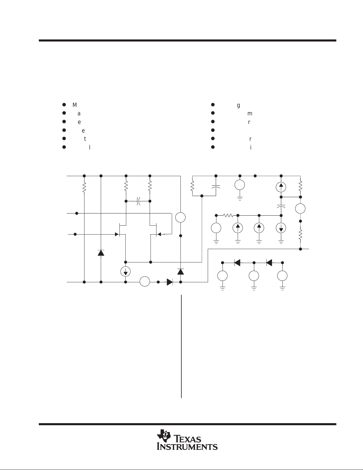
macromodel information
TLV2470, TLV2471, TLV2472, TLV2473, TLV2474, TLV2475, TLV247xA
FAMILY OF 600-µA/Ch 2.8-MHz RAIL-TO-RAIL INPUT/OUTPUT
HIGH-DRIVE OPERATIONAL AMPLIFIERS WITH SHUTDOWN
SLOS232B – JUNE 1999 – REVISED MARCH 2000
APPLICATION INFORMATION
Macromodel information provided was derived using Microsim
with Microsim
PSpice
. The Boyle macromodel (see Note 2) and subcircuit in Figure 55 are generated using
Parts
, the model generation software used
the TLV247x typical electrical and operating characteristics at TA = 25°C. Using this information, output
simulations of the following key parameters can be generated to a tolerance of 20% (in most cases):
D
Maximum positive output voltage swing
D
Maximum negative output voltage swing
D
Slew rate
D
Quiescent power dissipation
D
Input bias current
D
Open-loop voltage amplification
NOTE 1: G. R. Boyle, B. M. Cohn, D. O. Pederson, and J. E. Solomon, “Macromodeling of Integrated Circuit Operational Amplifiers,”
of Solid-State Circuits,
V
DD
rp
IN+
1
2
IN–
SC-9, 353 (1974).
3
rd1 rd2
c1
11 12
DSD
G
dp
10
+
vc
–
G
S
53
rss
D
Unity-gain frequency
D
Common-mode rejection ratio
D
Phase margin
D
DC output resistance
D
AC output resistance
D
Short-circuit output current limit
99
+
css
r2
96
+
vb
–
91 90 92
egnd
–
ioffgcm
dlp dln
fb
c2
ga
ro2
+
–
ro1
5
IEEE Journal
7
vlim
8
OUT
iss
GND
* TLV247x operational amplifier ”macromodel” subcircuit
* created using Parts release 8.0 on 4/27/99 at 14:31
* Parts is a MicroSim product.
*
* connections: non–inverting input
* | inverting input
* | | positive power supply
* | | | negative power supply
* | | | | output
* | | | | |
.subckt TLV247x 1 2 3 4 5
*
egnd 99 0 poly(2) (3,0) (4,0) 0 .5 .5
fb 7 99 poly(5) vb vc ve vlp vln 0
ga 6 0 11 12 79.828E–6
gcm 0 6 10 99 32.483E–9
c1 11 12 1.1094E–12
c2 6 7 5.5000E–12
css 10 99 556.53E–15
dc 5 53 dy
de 54 5 dy
dlp 90 91 dx
dln 92 90 dx
dp 4 3 dx
+ 39.614E6 –1E3 1E3 40E6 –40E6
4
–
ve
Figure 55. Boyle Macromodel and Subcircuit
PSpice
and
Parts
are trademarks of MicroSim Corporation.
dc
+
54
de
iss 10 4 dc 10.714E–6
hlim 90 0 vlim 1K
ioff 0 6 dc 75E–9
j1 11 2 10 jx1
j2 12 1 10 jx2
r2 6 9 100.00E3
rd1 3 11 12.527E3
rd2 3 12 12.527E3
ro1 8 5 10
ro2 7 99 10
rp 3 4 3.8023E3
vb 9 0 dc 0
vc 3 53 dc .842
ve 54 4 dc .842
vlim 7 8 dc 0
vlp 91 0 dc 110
vln 0 92 dc 110
rss 10 99 18.667E6
.model dx D(Is=800.00E–18)
.model dy D(Is=800.00E–18 Rs=1m Cjo=10p)
.model jx1 NJF(Is=1.0825E–12 Beta=594.78E–06 + Vto=–1)
.model jx2 NJF(Is=1.0825E–12 Beta=594.78E–06 + Vto=–1)
.ends
*$
+
+
––
–
vlnhlimvlp
+
POST OFFICE BOX 655303 • DALLAS, TEXAS 75265
23

TLV2470, TLV2471, TLV2472, TLV2473, TLV2474, TLV2475, TLV247xA
FAMILY OF 600-µA/Ch 2.8-MHz RAIL-TO-RAIL INPUT/OUTPUT
HIGH-DRIVE OPERATIONAL AMPLIFIERS WITH SHUTDOWN
SLOS232B – JUNE 1999 – REVISED MARCH 2000
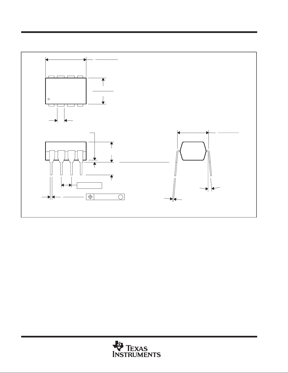
MECHANICAL DATA
D (R-PDSO-G**) PLASTIC SMALL-OUTLINE PACKAGE
14 PIN SHOWN
0.050 (1,27)
14
1
0.069 (1,75) MAX
A
0.020 (0,51)
0.014 (0,35)
0.010 (0,25)
0.004 (0,10)
DIM
8
7
PINS **
0.010 (0,25)
0.157 (4,00)
0.150 (3,81)
M
0.244 (6,20)
0.228 (5,80)
Seating Plane
0.004 (0,10)
8
14
0.008 (0,20) NOM
0°–8°
16
Gage Plane
0.010 (0,25)
0.044 (1,12)
0.016 (0,40)
A MAX
A MIN
NOTES: A. All linear dimensions are in inches (millimeters).
24
B. This drawing is subject to change without notice.
C. Body dimensions do not include mold flash or protrusion, not to exceed 0.006 (0,15).
POST OFFICE BOX 655303 • DALLAS, TEXAS 75265
0.197
(5,00)
0.189
(4,80)
0.344
(8,75)
0.337
(8,55)
0.394
(10,00)
0.386
(9,80)
4040047/D 10/96
TLV2470, TLV2471, TLV2472, TLV2473, TLV2474, TLV2475, TLV247xA
FAMILY OF 600-µA/Ch 2.8-MHz RAIL-TO-RAIL INPUT/OUTPUT
HIGH-DRIVE OPERATIONAL AMPLIFIERS WITH SHUTDOWN
SLOS232B – JUNE 1999 – REVISED MARCH 2000
MECHANICAL INFORMATION
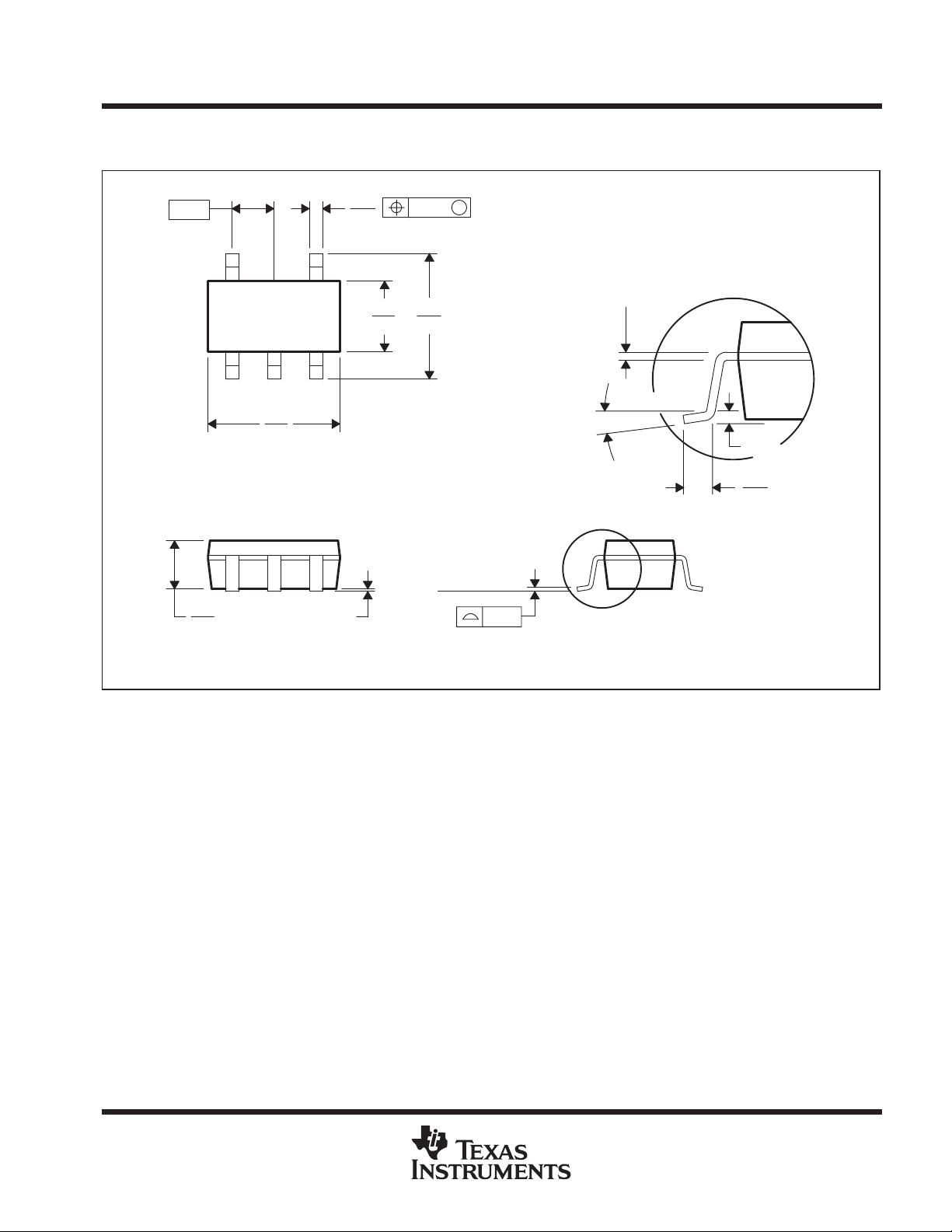
DBV (R-PDSO-G5) PLASTIC SMALL-OUTLINE PACKAGE
0,95
1,30
1,00
0,40
0,20
45
1,80
1,50
1
3,10
2,70
3
0,05 MIN
M
0,25
3,00
2,50
Seating Plane
0,10
0,15 NOM
0°–8°
Gage Plane
0,25
0,55
0,35
NOTES: A. All linear dimensions are in millimeters.
B. This drawing is subject to change without notice.
C. Body dimensions include mold flash or protrusion.
4073253-4/B 10/97
POST OFFICE BOX 655303 • DALLAS, TEXAS 75265
25
TLV2470, TLV2471, TLV2472, TLV2473, TLV2474, TLV2475, TLV247xA
FAMILY OF 600-µA/Ch 2.8-MHz RAIL-TO-RAIL INPUT/OUTPUT
HIGH-DRIVE OPERATIONAL AMPLIFIERS WITH SHUTDOWN
SLOS232B – JUNE 1999 – REVISED MARCH 2000
MECHANICAL INFORMATION
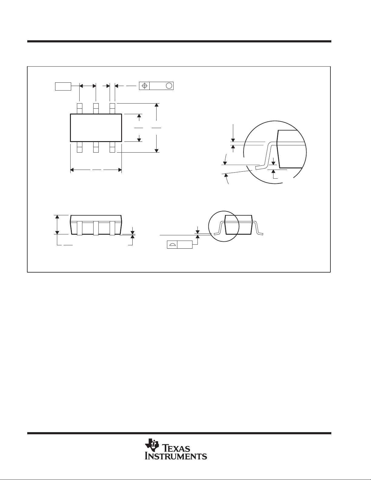
DBV (R-PDSO-G6) PLASTIC SMALL-OUTLINE PACKAGE
0,95
1,30
1,00
0,40
0,20
46
1,80
1,50
1
3,10
2,70
3
0,05 MIN
M
0,25
3,00
2,50
Seating Plane
0,15 NOM
Gage Plane
0,25
0°–8°
0,10
NOTES: A. All linear dimensions are in millimeters.
B. This drawing is subject to change without notice.
C. Body dimensions include mold flash or protrusion.
4073253-5/B 10/97
26
POST OFFICE BOX 655303 • DALLAS, TEXAS 75265
TLV2470, TLV2471, TLV2472, TLV2473, TLV2474, TLV2475, TLV247xA
FAMILY OF 600-µA/Ch 2.8-MHz RAIL-TO-RAIL INPUT/OUTPUT
HIGH-DRIVE OPERATIONAL AMPLIFIERS WITH SHUTDOWN
SLOS232B – JUNE 1999 – REVISED MARCH 2000
MECHANICAL INFORMATION
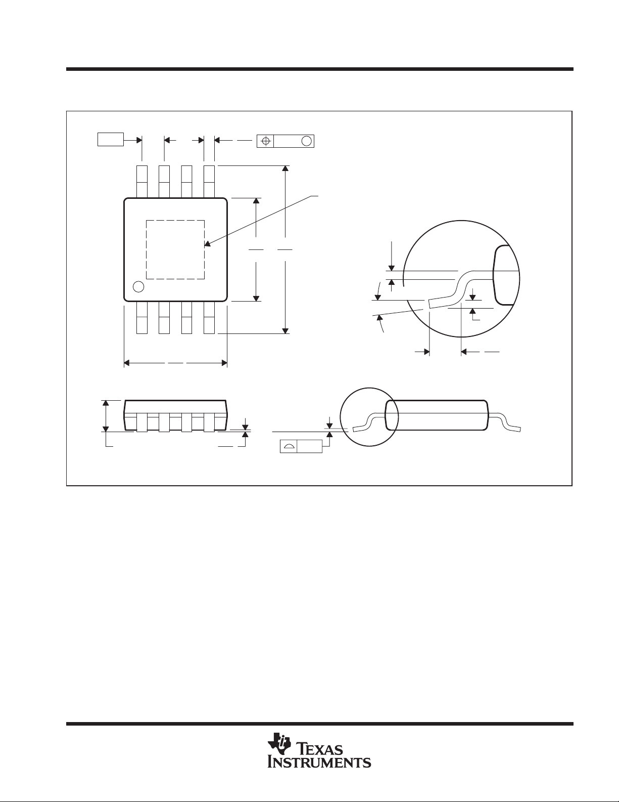
DGN (S-PDSO-G8) PowerPAD PLASTIC SMALL-OUTLINE PACKAGE
0,65
8
1
1,07 MAX
3,05
2,95
0,38
0,25
5
3,05
2,95
4
Seating Plane
0,15
0,05
0,25
4,98
4,78
M
0,10
Thermal Pad
(See Note D)
0,15 NOM
0°–6°
Gage Plane
0,25
0,69
0,41
NOTES: A. All linear dimensions are in millimeters.
B. This drawing is subject to change without notice.
C. Body dimensions include mold flash or protrusions.
D. The package thermal performance may be enhanced by attaching an external heat sink to the thermal pad.
This pad is electrically and thermally connected to the backside of the die and possibly selected leads. The dimension of the thermal
pad is 68 mils (height as illustrated) × 70 mils (width as illustrated) (maximum). The pad is centered on the bottom of the package.
E. Falls within JEDEC MO-187
PowerPAD is a trademark of Texas Instruments Incorporated.
4073271/A 04/98
POST OFFICE BOX 655303 • DALLAS, TEXAS 75265
27

TLV2470, TLV2471, TLV2472, TLV2473, TLV2474, TLV2475, TLV247xA
FAMILY OF 600-µA/Ch 2.8-MHz RAIL-TO-RAIL INPUT/OUTPUT
HIGH-DRIVE OPERATIONAL AMPLIFIERS WITH SHUTDOWN
SLOS232B – JUNE 1999 – REVISED MARCH 2000
MECHANICAL INFORMATION
DGQ (S-PDSO-G10) PowerPAD PLASTIC SMALL-OUTLINE PACKAGE
0,50
10
1
1,07 MAX
3,05
2,95
0,27
0,17
6
3,05
2,95
5
Seating Plane
0,15
0,05
0,25
4,98
4,78
M
0,10
Thermal Pad
(See Note D)
0,15 NOM
Gage Plane
0°–6°
0,25
0,69
0,41
NOTES: A. All linear dimensions are in millimeters.
PowerPAD is a trademark of Texas Instruments Incorporated.
28
B. This drawing is subject to change without notice.
C. Body dimensions do not include mold flash or protrusion.
D. The package thermal performance may be enhanced by bonding the thermal pad to an external thermal plane.
This pad is electrically and thermally connected to the backside of the die and possibly selected leads. The dimension of the thermal
pad is 68 mils (height as illustrated) × 70 mils (width as illustrated) (maximum). The pad is centered on the bottom of the package.
POST OFFICE BOX 655303 • DALLAS, TEXAS 75265
4073273/A 04/98
TLV2470, TLV2471, TLV2472, TLV2473, TLV2474, TLV2475, TLV247xA
FAMILY OF 600-µA/Ch 2.8-MHz RAIL-TO-RAIL INPUT/OUTPUT
HIGH-DRIVE OPERATIONAL AMPLIFIERS WITH SHUTDOWN
SLOS232B – JUNE 1999 – REVISED MARCH 2000
MECHANICAL INFORMATION
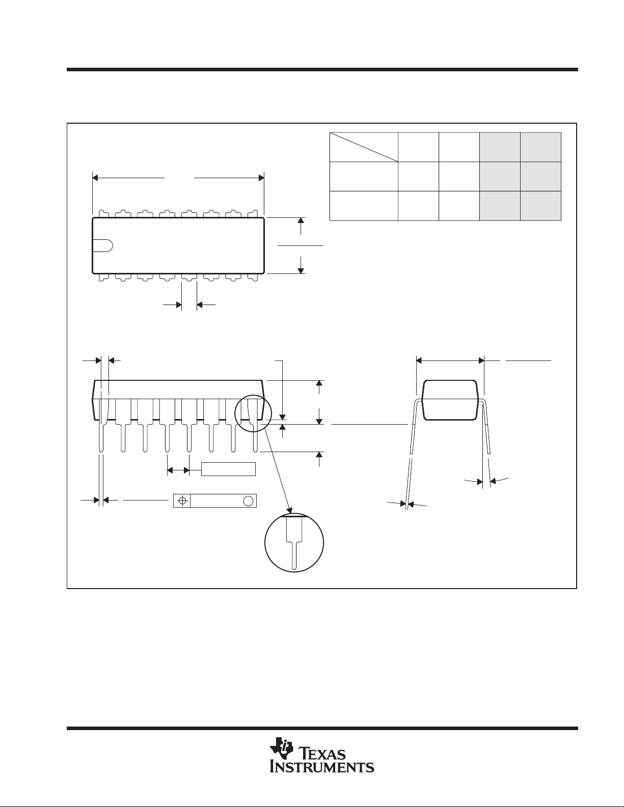
N (R-PDIP-T**) PLASTIC DUAL-IN-LINE PACKAGE
16 PIN SHOWN
16
1
0.035 (0,89) MAX
PINS **
DIM
A
9
0.260 (6,60)
0.240 (6,10)
8
0.070 (1,78) MAX
0.020 (0,51) MIN
0.200 (5,08) MAX
A MAX
A MIN
Seating Plane
14
0.775
(19,69)
0.745
(18,92)
16
0.775
(19,69)
0.745
(18,92)
18
0.920
(23.37)
0.850
(21.59)
20
0.975
(24,77)
0.940
(23,88)
0.310 (7,87)
0.290 (7,37)
0.100 (2,54)
0.021 (0,53)
0.015 (0,38)
NOTES: A. All linear dimensions are in inches (millimeters).
B. This drawing is subject to change without notice.
C. Falls within JEDEC MS-001 (20 pin package is shorter then MS-001.)
0.010 (0,25)
M
0.125 (3,18) MIN
0°–15°
0.010 (0,25) NOM
14/18 PIN ONL Y
4040049/C 08/95
POST OFFICE BOX 655303 • DALLAS, TEXAS 75265
29
TLV2470, TLV2471, TLV2472, TLV2473, TLV2474, TLV2475, TLV247xA
FAMILY OF 600-µA/Ch 2.8-MHz RAIL-TO-RAIL INPUT/OUTPUT
HIGH-DRIVE OPERATIONAL AMPLIFIERS WITH SHUTDOWN
SLOS232B – JUNE 1999 – REVISED MARCH 2000
MECHANICAL INFORMATION
P (R-PDIP-T8) PLASTIC DUAL-IN-LINE PACKAGE
0.400 (10,60)
0.355 (9,02)
58
0.260 (6,60)
0.240 (6,10)
41
0.070 (1,78) MAX
0.020 (0,51) MIN
0.200 (5,08) MAX
0.125 (3,18) MIN
0.100 (2,54)
0.021 (0,53)
0.015 (0,38)
NOTES: A. All linear dimensions are in inches (millimeters).
B. This drawing is subject to change without notice.
C. Falls within JEDEC MS-001
0.010 (0,25)
M
0.310 (7,87)
0.290 (7,37)
Seating Plane
0°–15°
0.010 (0,25) NOM
4040082/B 03/95
30
POST OFFICE BOX 655303 • DALLAS, TEXAS 75265
TLV2470, TLV2471, TLV2472, TLV2473, TLV2474, TLV2475, TLV247xA
FAMILY OF 600-µA/Ch 2.8-MHz RAIL-TO-RAIL INPUT/OUTPUT
HIGH-DRIVE OPERATIONAL AMPLIFIERS WITH SHUTDOWN
SLOS232B – JUNE 1999 – REVISED MARCH 2000
MECHANICAL INFORMATION
PWP (R-PDSO-G**) PowerPAD PLASTIC SMALL-OUTLINE
20 PINS SHOWN
0,65
20
1
1,20 MAX
0,30
0,19
11
4,50
4,30
10
A
0,15
0,05
PINS **
DIM
M
0,10
6,60
6,20
Seating Plane
0,10
1614
Thermal Pad
(See Note D)
20
0,15 NOM
0°–8°
Gage Plane
0,25
0,75
0,50
2824
A MAX
A MIN
NOTES: A. All linear dimensions are in millimeters.
B. This drawing is subject to change without notice.
C. Body dimensions do not include mold flash or protrusions.
D. The package thermal performance may be enhanced by bonding the thermal pad to an external thermal plane.
This pad is electrically and thermally connected to the backside of the die and possibly selected leads. The dimension of the thermal
pad is 78 mils (height as illustrated) × 94 mils (width as illustrated) (maximum). The pad is centered on the bottom of the package.
E. Falls within JEDEC MO-153
5,10
4,90
5,10
4,90
6,60
6,40
7,90
7,70
9,80
9,60
4073225/F 10/98
POST OFFICE BOX 655303 • DALLAS, TEXAS 75265
31

IMPORTANT NOTICE
T exas Instruments and its subsidiaries (TI) reserve the right to make changes to their products or to discontinue
any product or service without notice, and advise customers to obtain the latest version of relevant information
to verify, before placing orders, that information being relied on is current and complete. All products are sold
subject to the terms and conditions of sale supplied at the time of order acknowledgment, including those
pertaining to warranty, patent infringement, and limitation of liability.
TI warrants performance of its semiconductor products to the specifications applicable at the time of sale in
accordance with TI’s standard warranty. Testing and other quality control techniques are utilized to the extent
TI deems necessary to support this warranty . Specific testing of all parameters of each device is not necessarily
performed, except those mandated by government requirements.
Customers are responsible for their applications using TI components.
In order to minimize risks associated with the customer’s applications, adequate design and operating
safeguards must be provided by the customer to minimize inherent or procedural hazards.
TI assumes no liability for applications assistance or customer product design. TI does not warrant or represent
that any license, either express or implied, is granted under any patent right, copyright, mask work right, or other
intellectual property right of TI covering or relating to any combination, machine, or process in which such
semiconductor products or services might be or are used. TI’s publication of information regarding any third
party’s products or services does not constitute TI’s approval, warranty or endorsement thereof.
Copyright 2000, Texas Instruments Incorporated
 Loading...