

Datasheet TLV2462CD, TLV2462CDGK, TLV2465AID, TLV2464IPWR, TLV2464IPW Datasheet (Texas Instruments)
...
DEVICE
NO. OF Ch
SHUTDOWN
Selecti
(
OU060)
(Lit# SLOU060)
TLV2460, TLV2461, TLV2462, TLV2463, TLV2464, TLV2465, TLV246xA
FAMILY OF LOW-POWER RAIL-TO-RAIL INPUT/OUTPUT
OPERATIONAL AMPLIFIERS WITH SHUTDOWN
SLOS220F – JULY 1998 – REVISED OCT OBER 1999
D
Input Common-Mode Range Exceeds Both
Supply Rails ... – 0.2V to V
D
Gain Bandwidth Product . . . 6.4MHz
D
Supply Current ...500µA/channel
D
Input Offset Voltage . . . 100 µV
D
Input Noise Voltage ...11nV/√Hz
D
Rail-to-Rail Output Swing
D
Slew Rate . . . 1.6 V/µs
D
±90mA Output Drive Capability
D
Micropower Shutdown Mode
DD+
+ 0.2V
OUT
GND
IN+
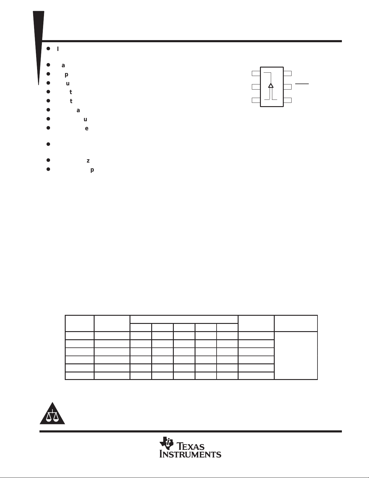
TLV2460
DBV PACKAGE
(TOP VIEW)
1
6
2
5
3
4
V
DD+
SHDN
IN–
(TLV2460/3/5) . . . 0.3 µA/channel
D
Available in 5- or 6-pin SOT23 and
8- or 10-Pin MSOP
D
Characterized From T
D
Universal Op Amp EVM
= –40°C to 125°C
A
description
The TLV246x is a family of low-power rail-to-rail input/output operational amplifiers specifically designed for
portable applications. The input common-mode voltage range extends beyond the supply rails for maximum
dynamic range in low-voltage systems. The amplifier output has rail-to-rail performance with high-output-drive
capability, solving one of the limitations of older rail-to-rail input/output operational amplifiers. This rail-to-rail
dynamic range and high output drive make the TLV246x ideal for buffering analog-to-digital converters.
The operational amplifier has 6.4 MHz of bandwidth and 1.6 V/µs of slew rate with only 500 µA of supply current,
providing good ac performance with low power consumption. Three members of the family offer a shutdown
terminal, which places the amplifier in an ultra-low supply current mode (I
= 0.3 µA/ch). While in shutdown,
DD
the operational-amplifier output is placed in a high-impedance state. DC applications are also well served with
an input noise voltage of 11 nV/√Hz and input offset voltage of 100 µV.
This family is available in the low-profile SOT23, MSOP, and TSSOP packages. The TLV2460 is the first
rail-to-rail input/output operational amplifier with shutdown available in the 6-pin SOT23, making it perfect for
high-density circuits. The family is specified over an expanded temperature range (T
= –40°C to 125°C) for
A
use in industrial control and automotive systems.
FAMILY PACKAGE TABLE
PACKAGE TYPES
PDIP SOIC SOT-23 TSSOP MSOP
TLV2460 1 8 8 6 — — Yes
TLV2461 1 8 8 5 — — —
TLV2462 2 8 8 — — 8 —
TLV2463 2 14 14 — — 10 Yes
TLV2464 4 14 14 — 14 — —
TLV2465 4 16 16 — 16 — Yes
UNIVERSAL
EVM BOARD
Refer to the EVM
on Guide
Lit# SL
Please be aware that an important notice concerning availability, standard warranty, and use in critical applications of
Texas Instruments semiconductor products and disclaimers thereto appears at the end of this data sheet.
This document contains information on products in more than one phase
of development. The status of each device is indicated on the page(s)
specifying its electrical characteristics.
POST OFFICE BOX 655303 • DALLAS, TEXAS 75265
Copyright 1999, Texas Instruments Incorporated
1
TLV2460, TLV2461, TLV2462, TLV2463, TLV2464, TLV2465, TLV246xA
V
CHIP FORM
‡
40°C to 125°C
V
CHIP FORM
‡
V
CHIP FORM
‡
6 Pin
SOT-23
5 Pin
8 Pin
MSOP
10 Pin
FAMILY OF LOW-POWER RAIL-TO-RAIL INPUT/OUTPUT
OPERATIONAL AMPLIFIERS WITH SHUTDOWN
SLOS220F – JULY 1998 – REVISED OCT OBER 1999
TLV2460 and TLV2461 AVAILABLE OPTIONS
max
T
A
0°C to 70°C 2000 µV
°
-
†
This package is available taped and reeled. To order this packaging option, add an R suffix to the part number (e.g., TLV2460CDR).
‡
Chip forms are tested at TA = 25°C only.
T
A
0°C to
70°C
–40°C to
125°C
†
This package is available taped and reeled. To order this packaging option, add an R suffix to the part number (e.g., TLV2462CDR).
‡
Chip forms are tested at TA = 25°C only.
AT 25°C
2000 µV
2000 µV
1500 µV
IO
max
°
SMALL OUTLINE
IO
AT 25°C
2000 µV
1500 µV
(D)
TLV2462CD
TLV2463CD
TLV2462ID
TLV2463ID
TLV2462AID
TLV2463AID
SMALL OUTLINE
(D)
TLV2460CD
TLV2461CD
TLV2460ID
TLV2461ID
TLV2460AID
TLV2461AID
TLV2462 and TLV2463 AVAILABLE OPTIONS
†
MSOP
(DGK)
TLV2462CDGK
—
TLV2462IDGK
—
—
—
PACKAGED DEVICES
SOT-23
(DBV)
TLV2460CDBV
TLV2461CDBV
TLV2460IDBV
TLV2461IDBV
—
—
PACKAGED DEVICES
†
MSOP
(DGS)
—
TLV2463CDGS—TLV2463CN
—
TLV2463IDGS
—
—
†
PLASTIC DIP
TLV2463IN
TLV2463AIN
PLASTIC DIP
TLV2460CP
TLV2461CP
TLV2460IP
TLV2461IP
TLV2460AIP
TLV2461AIP
(N)
—
—
(P)
TLV2460Y
TLV2461Y
PLASTIC DIP
(P)
TLV2462CP
—
TLV2462IP
—
TLV2462AIP
—
(Y)
—
—
—
—
(Y)
TLV2462Y
TLV2463Y
—
—
—
—
TLV2464 and TLV2465 AVAILABLE OPTIONS
max
T
A
0°C to 70°C 2000 µV
–40°C to 125°C 2000 µV
–40°C to 125°C 1500 µV
†
This package is available taped and reeled. To order this packaging option, add an R suffix to the part number
(e.g., TLV2464CDR).
‡
Chip forms are tested at TA = 25°C only.
DEVICE TYPE
IO
AT 25°C
SMALL OUTLINE
(D)
TLV2464CD
TLV2465CD
TLV2464ID
TLV2465ID
TLV2464AID
TLV2465AID
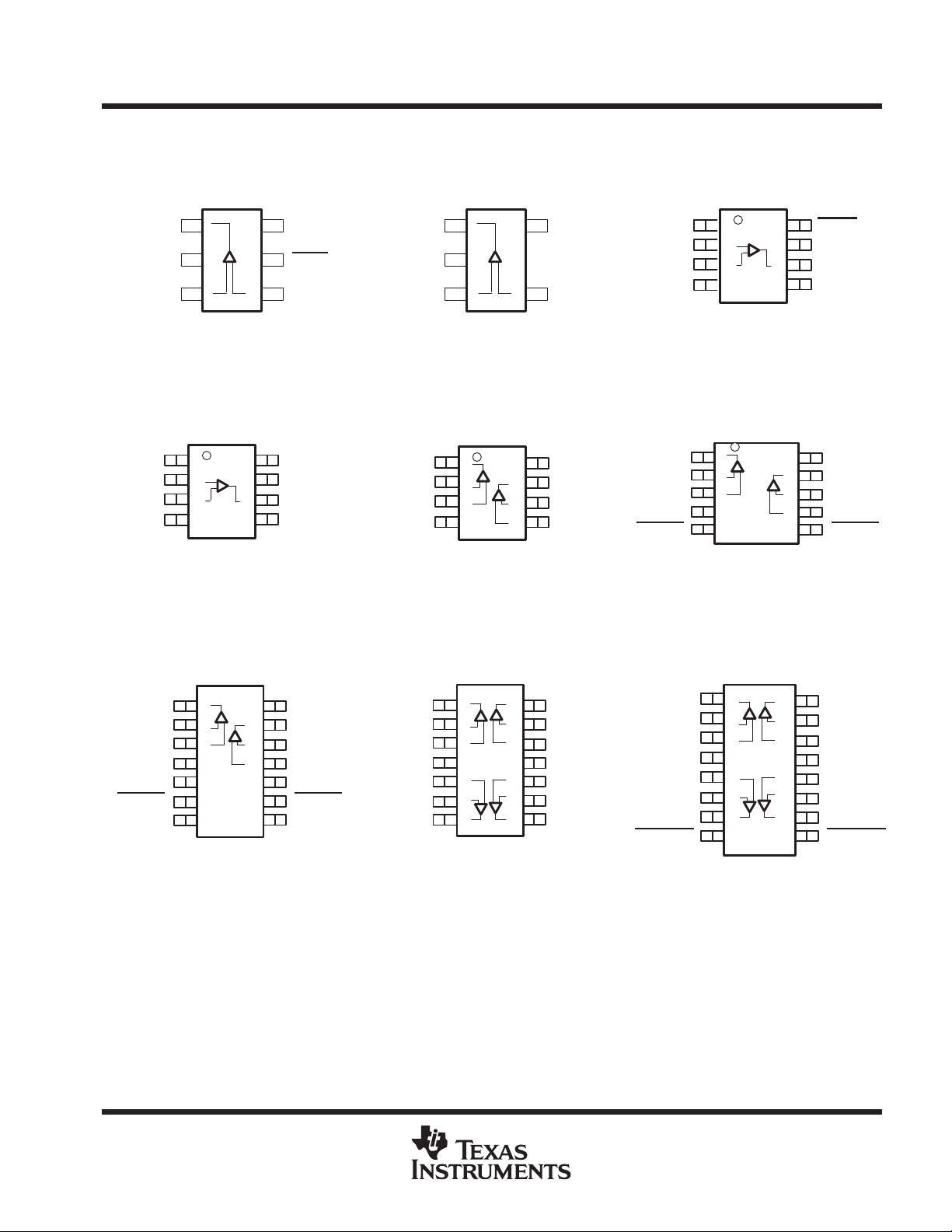
SOT-23 AND MSOP DEVICE SYMBOLS
NO. OF
TERMINALS
PACKAGED DEVICES
PLASTIC DIP
(N)
TLV2464CN
TLV2465CN
TLV2464IN
TLV2465IN
TLV2464AIN
TLV2465AIN
PACKAGE NAME SYMBOL
TLV2460CDBV VAOC
TLV2460IDBV VAOI
TLV2461CDBV VAPC
TLV2461IDBV VAPI
TLV2462CDGK xxTIAAI
TLV2462IDGK xxTIAAJ
TLV2463CDGS xxTIAAK
TLV2463IDGS xxTIAAL
TSSOP
(PW)
TLV2464CPW
TLV2465CPW
TLV2464IPW
TLV2465IPW
TLV2464AIPW
TLV2465AIPW
(Y)
TLV2464Y
TLV2465Y
—
—
—
—
2
POST OFFICE BOX 655303 • DALLAS, TEXAS 75265
TLV2460, TLV2461, TLV2462, TLV2463, TLV2464, TLV2465, TLV246xA
FAMILY OF LOW-POWER RAIL-TO-RAIL INPUT/OUTPUT
OPERATIONAL AMPLIFIERS WITH SHUTDOWN
SLOS220F – JULY 1998 – REVISED OCT OBER 1999
TLV246x PACKAGE PINOUTS
OUT
GND
IN+
D OR P PACKAGE
NC
IN–
IN+
GND
TLV2460
DBV PACKAGE
(TOP VIEW)
1
6
2
5
3
4
TLV2461
(TOP VIEW)
1
8
2
7
3
6
4
5
V
DD+
SHDN
IN–
NC
V
DD
OUT
NC
TLV2461
DBV PACKAGE
(TOP VIEW)
OUT
1
V
5
DD+
NC
IN–
GND
IN+
D, DGK, OR P PACKAGE
1OUT
+
1IN–
1IN+
GND
2
3
4
TLV2462
(TOP VIEW)
1
8
2
7
3
6
4
5
IN–
V
DD
2OUT
2IN–
2IN+
IN+
GND
+
1OUT
1IN–
1IN+
GND
1SHDN
TLV2460
D OR P PACKAGE
(TOP VIEW)
1
2
3
4
DGS PACKAGE
(TOP VIEW)
1
2
3
4
5
8
7
6
5
TLV2463
10
9
8
7
6
SHDN
VDD+
OUT
NC
VDD+
2OUT
2IN–
2IN+
2SHDN
TLV2463
D OR N PACKAGE
(TOP VIEW)
1OUT
1IN–
1IN+
GND
NC
1SHDN
NC
NC – No internal connection
1
14
2
13
3
12
4
11
5
10
6
7
D, N, OR PWP PACKAGE
V
+
DD
2OUT
2IN–
2IN+
NC
2SHDN
9
8
NC
1OUT
1IN–
1IN+
V
DD
2IN+
2IN–
2OUT
+
TLV2464
(TOP VIEW)
1
14
2
13
3
12
4
11
5
10
6
7
9
8
4OUT
4IN–
4IN+
GND
3IN+
3IN–
3OUT
D, N, OR PWP PACKAGE
1OUT
1IN–
1IN+
V
+
DD
2IN+
2IN–
2OUT
1/2SHDN
TLV2465
(TOP VIEW)
1
16
2
15
3
14
4
13
5
12
6
11
7
10
8
9
4OUT
4IN–
4IN+
GND
3IN+
3IN–
3OUT
3/4SHDN
POST OFFICE BOX 655303 • DALLAS, TEXAS 75265
3
TLV2460, TLV2461, TLV2462, TLV2463, TLV2464, TLV2465, TLV246xA
PACKAGE
JC
JA
A
Suppl
oltage, V
V
Operating free-air temperature, T
°C
FAMILY OF LOW-POWER RAIL-TO-RAIL INPUT/OUTPUT
OPERATIONAL AMPLIFIERS WITH SHUTDOWN
SLOS220F – JULY 1998 – REVISED OCT OBER 1999
absolute maximum ratings over operating free-air temperature range (unless otherwise noted)
†
Supply voltage, VDD (see Note 1) 6 V. . . . . . . . . . . . . . . . . . . . . . . . . . . . . . . . . . . . . . . . . . . . . . . . . . . . . . . . . . . . .
Differential input voltage, VID V
Input current, I
(any input) ± 200 mA. . . . . . . . . . . . . . . . . . . . . . . . . . . . . . . . . . . . . . . . . . . . . . . . . . . . . . . . . . . . .
I
DD
– 0.2 V to VDD + 0.2 V. . . . . . . . . . . . . . . . . . . . . . . . . . . . . . . . . . . . . . . . . . .
Output current, IO ± 175 mA. . . . . . . . . . . . . . . . . . . . . . . . . . . . . . . . . . . . . . . . . . . . . . . . . . . . . . . . . . . . . . . . . . . . .
Total input current, II (into V
) 175 mA. . . . . . . . . . . . . . . . . . . . . . . . . . . . . . . . . . . . . . . . . . . . . . . . . . . . . . . . . .
DD+
Total output current, IO (out of GND) 175 mA. . . . . . . . . . . . . . . . . . . . . . . . . . . . . . . . . . . . . . . . . . . . . . . . . . . . . .
Continuous total power dissipation See Dissipation Rating Table. . . . . . . . . . . . . . . . . . . . . . . . . . . . . . . . . . . . .
Operating free-air temperature range, T
: C suffix 0°C to 70°C. . . . . . . . . . . . . . . . . . . . . . . . . . . . . . . . . . . . . .
A
I suffix –40°C to 125°C. . . . . . . . . . . . . . . . . . . . . . . . . . . . . . . . . . . .
Maximum junction temperature, TJ 150°C. . . . . . . . . . . . . . . . . . . . . . . . . . . . . . . . . . . . . . . . . . . . . . . . . . . . . . . . .
Storage temperature range, T
–65°C to 150°C. . . . . . . . . . . . . . . . . . . . . . . . . . . . . . . . . . . . . . . . . . . . . . . . . . .
stg
Lead temperature 1,6 mm (1/16 inch) from case for 10 seconds 260°C. . . . . . . . . . . . . . . . . . . . . . . . . . . . . . .
†
Stresses beyond those listed under “absolute maximum ratings” may cause permanent damage to the device. These are stress ratings only, and
functional operation of the device at these or any other conditions beyond those indicated under “recommended operating conditions” is not
implied. Exposure to absolute-maximum-rated conditions for extended periods may affect device reliability.
NOTE 1: All voltage values, except differential voltages, are with respect to GND.
DISSIPATION RATING TABLE
Θ
(°C/W)
D (8) 38.3 176 725 mW
D (14) 26.9 122.6 725 mW
D (16) 25.7 114.7 725 mW
DBV (5) 55 324.1 437 mW
DBV (6) 55 294.3 437 mW
DGK 54.23 259.96 424 mW
DGS 54.1 257.71 424 mW
N (14) 32 78 1150 mW
N (16) 32 78 1150 mW
P 41 104 1000 mW
PW (14) 29.3 173.6 700 mW
PW (16) 28.7 161.4 700 mW
Θ
(°C/W)
T
≤ 25°C
POWER RATING
recommended operating conditions
pp
y v
Common-mode input voltage range, V
p
4
DD
MIN MAX UNIT
Single supply 2.7 6
Split supply ±1.35 ±3
ICR
p
A
POST OFFICE BOX 655303 • DALLAS, TEXAS 75265
C-suffix 0 70
I-suffix
GND V
DD+
–40 125
V
°
PARAMETER
TEST CONDITIONS
T
†
UNIT
VIOInput offset voltage (TLV246x)
V
V
VIOInput offset voltage (TLV246xA)
O
V
2µV/°C
V
DD
IC
,
R
Ω
V
Common-mode input voltage range
V
I
mA
VOHHigh-level output voltage
V
I
mA
V
I
mA
VOLLow-level output voltage
V
V
I
mA
Sourcing
IOSShort-circuit output current
mA
Sinking
A
gg g
R
10 kΩ
dB
R
S
50 Ω
DD
,
IC DD
,
k
ygj
dB
DD
,
IC DD
,
TLV2460, TLV2461, TLV2462, TLV2463, TLV2464, TLV2465, TLV246xA
FAMILY OF LOW-POWER RAIL-TO-RAIL INPUT/OUTPUT
OPERATIONAL AMPLIFIERS WITH SHUTDOWN
SLOS220F – JULY 1998 – REVISED OCT OBER 1999
electrical characteristics at specified free-air temperature, VDD = 3 V (unless otherwise noted)
A
p
= ±1.5 V,
p
α
I
I
I
r
c
z
CMRR Common-mode rejection ratio
†
Full range is 0°C to 70°C for the C suffix and –40°C to 125°C for the I suffix. If not specified, full range is –40°C to 125°C.
Temperature coefficient of input offset
VIO
voltage
Input offset current
IO
Input bias current
IB
ICR
Output current 25°C ±30 mA
O
Large-signal differential voltage
VD
amplification
Differential input resistance 25°C 10
i(d)
Common-mode input capacitance f = 10 kHz 25°C 7 pF
i(c)
Closed-loop output impedance f = 100 kHz, AV = 10 25°C 33
o
Supply voltage rejection ratio
SVR
(∆VDD /∆VIO)
p
p
p
p
DD
VIC = 0,
= ±1.5 V,
VIC = 0,
VO = 0,
= 50
S
CMRR > 66 dB RS = 50 Ω 25°C
CMRR > 60 dB RS = 50 Ω Full range
= –2.5
OH
= –10
OH
= 1.5 V,
IC
= 1.5 V,
IC
=
L
V
= –0.2 V to 3.2 V,
ICR
=
V
= 2.7 V to 6 V, V
No load
= 3 V to 5 V, V
V
No load
VO = 0,
RS = 50 Ω
TLV246xC Full range 20
TLV246xI Full range 75
TLV246xC Full range 25
TLV246xI Full range 75
= 2.5
OL
= 10
OL
TLV246xC Full range 64
TLV246xI Full range 60
= V
/2,
= V
/2,
25°C 100 2000
Full range 2200
25°C
Full range
25°C 2.8 7
25°C 4.4 14
25°C 2.9
Full range 2.8
25°C 2.7
Full range 2.5
25°C 0.1
Full range 0.2
25°C 0.3
Full range 0.5
25°C 50
Full range 20
25°C 40
Full range 20
25°C 90 105
Full range 89
25°C 66 80
25°C 80 85
Full range 75
25°C 85 95
Full range 80
TLV246x
MIN TYP MAX
150 1500
1700
–0.2
to
3.2
–0.2
to
3.2
9
µ
µ
nA
nA
Ω
Ω
dB
°
POST OFFICE BOX 655303 • DALLAS, TEXAS 75265
5
TLV2460, TLV2461, TLV2462, TLV2463, TLV2464, TLV2465, TLV246xA
PARAMETER
TEST CONDITIONS
T
†
UNIT
IDDSupply current (per channels)
O
,
,
mA
V
Turnon voltage level
A
1
25°C
V
V
Turnoff voltage level
A
1
25°C
V
I
y
A
PARAMETER
TEST CONDITIONS
T
†
UNIT
V
C
160 pF
VnEquivalent input noise voltage
V/√H
V
O(PP)
()
R
L
kΩ
()
R
L
kΩ
V
,
tsSettling time
25°C
s
V
,
R
C
160 pF
FAMILY OF LOW-POWER RAIL-TO-RAIL INPUT/OUTPUT
OPERATIONAL AMPLIFIERS WITH SHUTDOWN
SLOS220F – JULY 1998 – REVISED OCT OBER 1999
electrical characteristics at specified free-air temperature, VDD = 3 V (unless otherwise noted)
(continued)
A
V
pp
(ON)
(OFF)
DD(SHDN)
†
Full range is 0°C to 70°C for the C suffix and –40°C to 125°C for the I suffix. If not specified, full range is –40°C to 125°C.
Supply current in shutdown
(TLV2460, TLV2463, TLV2465)
p
= 1.5 V, No load,
SHDN > 1.02 V
=
V
=
V
SHDN < 0.8 V, 25°C 0.3
Per channel in shutdown Full range 2.5
Channel 1
Channel 2
Channel 1
Channel 2
25°C 0.5 0.575
Full range 0.9
°
°
operating characteristics at specified free-air temperature, VDD = 3 V (unless otherwise noted)
A
= 2 V,
SR Slew rate at unity gain
p
I
n
THD + N Total harmonic distortion plus noise
t
(on)
t
(off)
φ
m
†
Full range is 0°C to 70°C for the C suffix and –40°C to 125°C for the I suffix. If not specified, full range is –40°C to 125°C.
Equivalent input noise current f = 1 kHz 25°C 0.13
Amplifier turnon time
Amplifier turnoff time
Gain-bandwidth product
Phase margin at unity gain
Gain margin
O(PP)
RL = 10 kΩ
f = 100 Hz 25°C 16
f = 1 kHz 25°C 11
=
= 2 V,
RL = 10 kΩ,
f = 1 kHz
AV = 1,
= 10
AV = 1,
= 10
f = 10 kHz,
CL = 160 pF
V
(STEP)PP
A
= –1,
CL = 10 pF,
RL = 10 kΩ
V
(STEP)PP
A
= –1,
CL = 56 pF,
RL = 10 kΩ
= 10 kΩ,
L
= 2 V,
= 2 V,
AV = 1 0.006%
AV = 10
AV = 100 0.08%
Both channels 7.6
Channel 1 only,
Channel 2 on
Channel 2 only,
Channel 1 on
Both channels 333
Channel 1 only,
Channel 2 on
Channel 2 only,
Channel 1 on
RL = 10 kΩ,
0.1% 1.47
0.01%
0.1%
0.01% 1.98
p
=
L
=
L
,
p
25°C
Full
range
25°C
25°C
25°C
25°C 5.2 MHz
°
25°C 44°
25°C 7 dB
TLV246x
MIN TYP MAX
1.021
1.02
0.822
0.817
TLV246x
MIN TYP MAX
1 1.6
0.8
0.02%
7.65
7.25
328
329
1.78
1.77
µ
V/µs
n
pA/√Hz
µs
ns
µ
z
6
POST OFFICE BOX 655303 • DALLAS, TEXAS 75265

PARAMETER
TEST CONDITIONS
T
†
UNIT
VIOInput offset voltage (TLV246x)
V
V
V
VIOInput offset voltage (TLV246xA)
O
V
25°C
2µV/°C
V
DD
IC
,
R
Ω
V
Common-mode input voltage range
V
I
mA
VOHHigh-level output voltage
V
I
mA
V
I
mA
VOLLow-level output voltage
V
V
I
mA
Sourcing
IOSShort-circuit output current
mA
Sinking
A
gg g
IC
,
L
,
dB
R
S
50 Ω
DD
,
IC DD
,
dB
k
ygj
DD
,
IC DD
,
dB
TLV2460, TLV2461, TLV2462, TLV2463, TLV2464, TLV2465, TLV246xA
FAMILY OF LOW-POWER RAIL-TO-RAIL INPUT/OUTPUT
OPERATIONAL AMPLIFIERS WITH SHUTDOWN
SLOS220F – JULY 1998 – REVISED OCT OBER 1999
electrical characteristics at specified free-air temperature, VDD = 5 V (unless otherwise noted)
A
p
= ±2.5 V,
p
α
I
I
I
r
c
z
CMRR Common-mode rejection ratio
†
Full range is 0°C to 70°C for the C suffix and –40°C to 125°C for the I suffix. If not specified, full range is –40°C to 125°C.
Temperature coefficient of input offset
VIO
voltage
Input offset current
IO
Input bias current
IB
ICR
Output current 25°C ±90 mA
O
Large-signal differential voltage V
VD
amplification
Differential input resistance 25°C 10
i(d)
Common-mode input capacitance f = 10 kHz 25°C 7 pF
i(c)
Closed-loop output impedance f = 100 kHz, AV = 10 25°C 29
o
Supply voltage rejection ratio
SVR
(∆VDD /∆VIO)
p
p
p
p
DD
VIC = 0,
= ±2.5 V,
VIC = 0,
VO = 0,
= 50
S
CMRR > 71 dB, RS = 50 Ω 25°C
CMRR > 60 dB, RS = 50 Ω Full range
= –2.5
OH
= –10
OH
= 2.5 V,
IC
= 2.5 V,
IC
= 2.5 V,
VO = 1 V to 4 V
V
= –0.2 V to 5.2 V,
ICR
=
=
V
= 2.7 V to 6 V, V
No load
= 3 V to 5 V, V
V
No load
= 0,
O
RS = 50 Ω
TLV246xC
TLV246xI
TLV246xC
TLV246xI
= 2.5
OL
= 10
OL
R
= 10 kΩ,
TLV246xC
TLV246xI
= V
= V
/2,
/2,
25°C 150 2000
Full range 2200
25°C
Full range
°
25°C 0.3 7
Full range 15
Full range 60
25°C 1.3 14
Full range 30
Full range 60
25°C 4.9
Full range 4.8
25°C 4.8
Full range 4.7
25°C 0.1
Full range 0.2
25°C 0.2
Full range 0.3
25°C 145
Full range 60
25°C 100
Full range 60
25°C 92 109
Full range 90
25°C 71 85
Full range 69
Full range 60
25°C 80 85
Full range 75
25°C 85 95
Full range 80
TLV246x
MIN TYP MAX
150 1500
1700
–0.2
to
5.2
0
to
5
9
µ
µ
nA
nA
Ω
Ω
dB
°
POST OFFICE BOX 655303 • DALLAS, TEXAS 75265
7

TLV2460, TLV2461, TLV2462, TLV2463, TLV2464, TLV2465, TLV246xA
PARAMETER
TEST CONDITIONS
T
†
UNIT
IDDSupply current (per channel)
O
,
,
mA
V
Turnon voltage level
A
1
25°C
V
V
Turnoff voltage level
A
1
25°C
V
I
y
A
PARAMETER
TEST CONDITIONS
T
†
UNIT
V
C
160 pF
VnEquivalent input noise voltage
V/√H
V
O(PP)
()
R
L
kΩ
()
R
L
kΩ
V
,
tsSettling time
25°C
s
V
,
R
C
160 pF
FAMILY OF LOW-POWER RAIL-TO-RAIL INPUT/OUTPUT
OPERATIONAL AMPLIFIERS WITH SHUTDOWN
SLOS220F – JULY 1998 – REVISED OCT OBER 1999
electrical characteristics at specified free-air temperature, VDD = 5 V (unless otherwise noted)
(continued)
A
V
pp
(ON)
(OFF)
DD(SHDN)
†
Full range is 0°C to 70°C for the C suffix and –40°C to 125°C for the I suffix. If not specified, full range is –40°C to 125°C.
Supply current in shutdown
(TLV2460, TLV2463, TLV2465)
p
= 2.5 V, No load,
SHDN > 1.38 V
=
V
=
V
SHDN < 1.3 V, 25°C 1
Per channels in shutdown Full range 3
Channel 1
Channel 2
Channel 1
Channel 2
25°C 0.55 0.65
Full range 1
°
°
operating characteristics at specified free-air temperature, VDD = 5 V (unless otherwise noted)
A
= 2 V,
SR Slew rate at unity gain
p
I
n
THD + N Total harmonic distortion plus noise
t
(on)
t
(off)
φ
m
†
Full range is 0°C to 70°C for the C suffix and –40°C to 125°C for the I suffix. If not specified, full range is –40°C to 125°C.
Equivalent input noise current f = 100 Hz 25°C 0.13
Amplifier turnon time
Amplifier turnoff time
Gain-bandwidth product
Phase margin at unity gain
Gain margin
O(PP)
RL = 10 kΩ
f = 100 Hz 25°C 14
f = 1 kHz 25°C 11
=
= 4 V,
RL = 10 kΩ,
f = 10 kHz
AV = 1,
= 10
AV = 1,
= 10
f = 10 kHz,
CL = 160 pF
V
(STEP)PP
A
= –1,
CL = 10 pF,
RL = 10 kΩ
V
(STEP)PP
A
= –1,
CL = 56 pF,
RL = 10 kΩ
= 10 kΩ,
L
= 2 V,
= 2 V,
AV = 1 0.004%
AV = 10
AV = 100 0.04%
Both channels 7.6
Channel 1 only,
Channel 2 on
Channel 2 only,
Channel 1 on
Both channels 333
Channel 1 only,
Channel 2 on
Channel 2 only,
Channel 1 on
RL = 10 kΩ,
0.1% 1.53
0.01%
0.1%
0.01% 3.33
p
=
L
=
L
,
p
25°C
Full
range
25°C
25°C
25°C
25°C 6.4 MHz
°
25°C 45°
25°C 7 dB
TLV246x
MIN TYP MAX
1.372
1.368
1.315
1.309
TLV246x
MIN TYP MAX
1 1.6
0.8
0.01%
7.65
7.25
328
329
1.83
3.13
µ
V/µs
n
pA/√Hz
µs
ns
µ
z
8
POST OFFICE BOX 655303 • DALLAS, TEXAS 75265
IDDSupply current
VnEquivalent input noise voltage
Gain bandwidth product
TLV2460, TLV2461, TLV2462, TLV2463, TLV2464, TLV2465, TLV246xA
FAMILY OF LOW-POWER RAIL-TO-RAIL INPUT/OUTPUT
OPERATIONAL AMPLIFIERS WITH SHUTDOWN
SLOS220F – JULY 1998 – REVISED OCT OBER 1999
TYPICAL CHARACTERISTICS
Table of Graphs
V
IO
I
IB
I
IO
V
OH
V
OL
V
O(PP)
A
VD
Z
o
CMRR Common-mode rejection ratio vs Frequency 17
k
SVR
SR Slew rate vs Supply voltage 27
THD Total harmonic distortion vs Frequency 32, 33
THD+N Total harmonic distortion plus noise vs Peak-to-peak signal amplitude 34, 35
φ
m
Input offset voltage vs Common-mode input voltage 1, 2
Input bias current vs Free-air temperature 3, 4
Input offset current vs Free-air temperature 3, 4
High-level output voltage vs High-level output current 5, 6
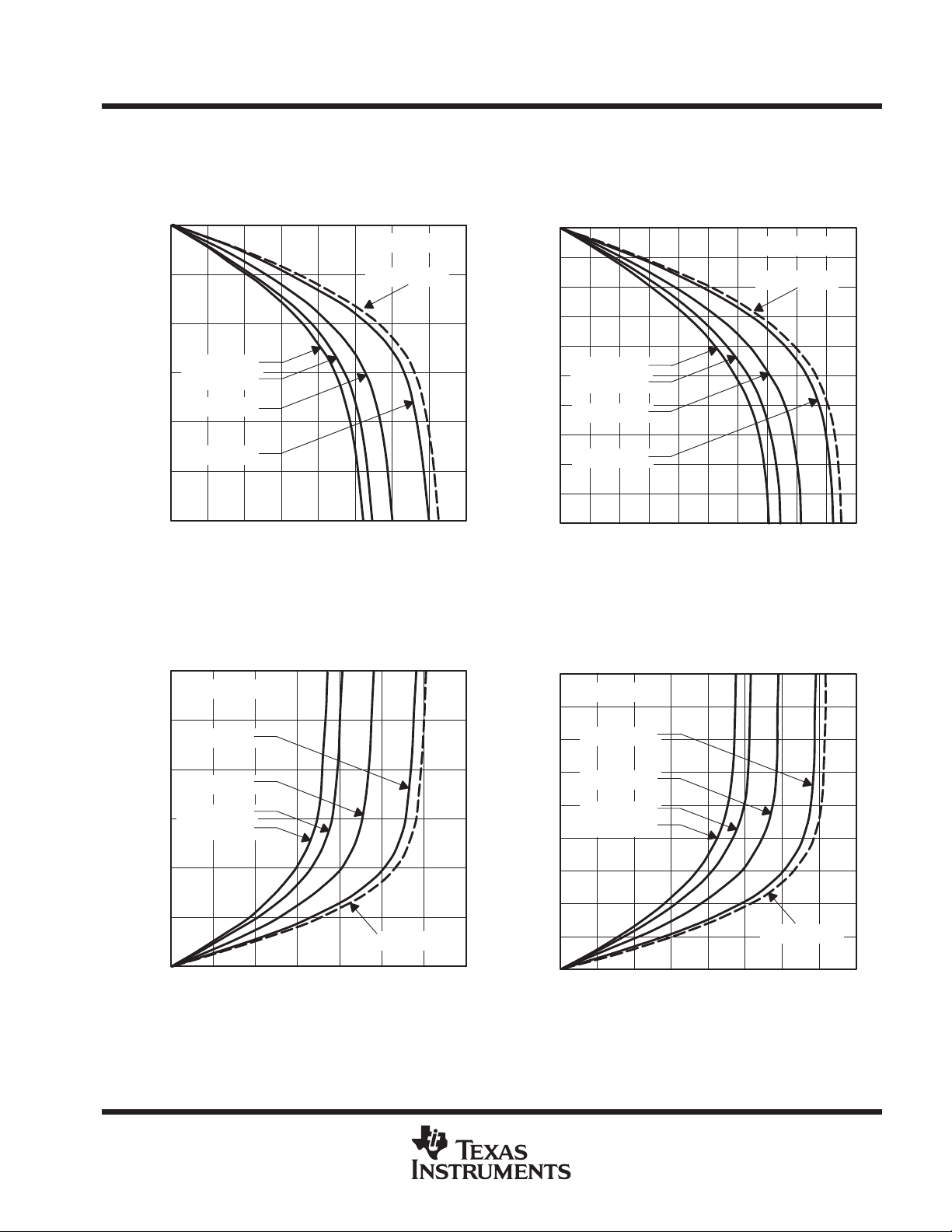
Low-level output voltage vs Low-level output current 7, 8
Peak-to-peak output voltage vs Frequency 9, 10
Open-loop gain vs Frequency 11, 12
Phase vs Frequency 11, 12
Differential voltage amplification vs Load resistance 13
Amplifier stability vs Load 14
Output impedance vs Frequency 15, 16
Supply-voltage rejection ratio vs Frequency 18, 19
pp
Amplifier turnon characteristics 22
Amplifier turnoff characteristics 23
Supply current turnon 24
Supply current turnoff 25
Shutdown supply current vs Free-air temperature 26
p
Phase margin
p
Large signal follower 40, 41
Small signal follower 42, 43
Inverting large signal 44, 45
Inverting small signal 46, 47
vs Supply voltage 20
vs Free-air temperature 21
vs Frequency 28, 29
vs Common-mode input voltage 30, 31
vs Frequency 11, 12
vs Load capacitance
vs Free-air temperature 37
vs Supply voltage 38
vs Free-air temperature 39
FIGURE
36
POST OFFICE BOX 655303 • DALLAS, TEXAS 75265
9
TLV2460, TLV2461, TLV2462, TLV2463, TLV2464, TLV2465, TLV246xA
FAMILY OF LOW-POWER RAIL-TO-RAIL INPUT/OUTPUT
OPERATIONAL AMPLIFIERS WITH SHUTDOWN
SLOS220F – JULY 1998 – REVISED OCT OBER 1999
TYPICAL CHARACTERISTICS
1
0.8
0.6
0.4
0.2
0
–0.2
–0.4
– Input Offset Voltage – mV
IO
V
–0.6
–0.8
–1
INPUT BIAS AND INPUT OFFSET CURRENT
5
4.5
4
3.5
3
2.5
INPUT OFFSET VOLTAGE
vs
COMMON-MODE INPUT VOLTAGE
VDD = 3 V
TA = 25°C
10.5 1.5 30 2 2.5
V
– Common-Mode Input Voltage – V
ICR
Figure 1
vs
FREE-AIR TEMPERATURE
I
IB
VDD = 3 V
VI = 1.5 V
1
0.8
0.6
0.4
0.2
0
–0.2
–0.4
– Input Offset Voltage – mV
IO
V
–0.6
–0.8
–1
INPUT BIAS AND INPUT OFFSET CURRENT
6
5
3
INPUT OFFSET VOLTAGE
vs
COMMON-MODE INPUT VOLTAGE
VDD = 5 V
TA = 25°C
213504
V
– Common-Mode Input Voltage – V
ICR
Figure 2
vs
FREE-AIR TEMPERATURE
I
IB
VDD = 5 V
VI = 2.5 V
2
1.5
1
– Input Bias and Input Offset Currents – nA
0.5
IO
0
and I
–0.5
–55
IB
I
I
IO
–35 5
–15 25 125
TA – Free-Air Temperature – °C
Figure 3
10
– Input Bias and Input Offset Currents – nA
IO
45 65
85 105
POST OFFICE BOX 655303 • DALLAS, TEXAS 75265
and I
IB
I
2
1
0
–1
I
IO
–35 5
–15 25 125–55
TA – Free-Air Temperature – °C
Figure 4
45 65485 105
TLV2460, TLV2461, TLV2462, TLV2463, TLV2464, TLV2465, TLV246xA
FAMILY OF LOW-POWER RAIL-TO-RAIL INPUT/OUTPUT
OPERATIONAL AMPLIFIERS WITH SHUTDOWN
SLOS220F – JULY 1998 – REVISED OCT OBER 1999
TYPICAL CHARACTERISTICS
HIGH-LEVEL OUTPUT VOLTAGE
vs
HIGH-LEVEL OUTPUT CURRENT
3
2.5
2
TA = 125°C
1.5
– High-Level Output Voltage – V
OH
0.5
V
TA = 85°C
TA = 25°C
1
TA = –40°C
0
0102030 60
IOH – High-Level Output Current – mA
Figure 5
LOW-LEVEL OUTPUT VOLTAGE
vs
LOW-LEVEL OUTPUT CURRENT
3
VDD = 3 V
2.5
TA = –40°C
DC
VDD = 3 V
TA = –55°C
5040 70 80
DC
HIGH-LEVEL OUTPUT VOLTAGE
HIGH-LEVEL OUTPUT CURRENT
5
4.5
4
3.5
3
TA = 125°C
2.5
1.5
– High-Level Output Voltage – V
OH
V
0.5
TA = 85°C
2
TA = 25°C
TA = –40°C
1
0
0 20 40 60 120
IOH – High-Level Output Current – mA
Figure 6
LOW-LEVEL OUTPUT VOLTAGE
LOW-LEVEL OUTPUT CURRENT
4.5
3.5
VDD = 5 V
4
TA = –40°C
DC
vs
VDD = 5 V
TA = –55°C
10080 140 200
DC
160 180
vs
2
TA = 25°C
TA = 85°C
1.5
TA = 125°C
1
OL
0.5
V – Low-Level Output Voltage – V
TA = –55°C
0
0102030 60
IOL – Low-Level Output Current – mA
5040 70
Figure 7
POST OFFICE BOX 655303 • DALLAS, TEXAS 75265
3
2.5
2
1.5
1
OL
V – Low-Level Output Voltage – V
0.5
0
TA = 25°C
TA = 85°C
TA = 125°C
0 204060 120
IOL – Low-Level Output Current – mA
Figure 8
TA = –55°C
10080 140
160
11
TLV2460, TLV2461, TLV2462, TLV2463, TLV2464, TLV2465, TLV246xA
FAMILY OF LOW-POWER RAIL-TO-RAIL INPUT/OUTPUT
OPERATIONAL AMPLIFIERS WITH SHUTDOWN
SLOS220F – JULY 1998 – REVISED OCT OBER 1999
TYPICAL CHARACTERISTICS
PEAK-TO-PEAK OUTPUT VOLTAGE
vs
FREQUENCY
3
2.5
2
1.5
1
– Peak-to-Peak Output Voltage – V
0.5
O(PP)
V
0
10k 100k 10M
f – Frequency – Hz
VDD = 3 V
AV = –10
THD = 1%
RL = 10 kΩ
1M
Figure 9
OPEN-LOOP GAIN AND PHASE
100
90
80
70
60
50
40
30
20
Open-Lopp Gain – dB
10
0
–10
–20
100 10k
10
5.5
5
4.5
4
3.5
3
2.5
2
1.5
– Peak-to-Peak Output Voltage – V
1
O(PP)
0.5
V
0
10k 100k 10M
vs
FREQUENCY
VDD = ±1.5 V
RL = 10 kΩ
CL = 0
TA = 25°C
A
VD
Phase
1k 100k 1M
f – Frequency – Hz
PEAK-TO-PEAK OUTPUT VOLTAGE
vs
FREQUENCY
VDD = 5 V
AV = –10
THD = 1%
RL = 10 kΩ
1M
f – Frequency – Hz
Figure 10
40°
20°
0°
–20°
–40°
–60°
10M
–80°
–100°
–120°
–140°
–160°
–180°
–200°
Phase
12
Figure 11
POST OFFICE BOX 655303 • DALLAS, TEXAS 75265

TLV2460, TLV2461, TLV2462, TLV2463, TLV2464, TLV2465, TLV246xA
FAMILY OF LOW-POWER RAIL-TO-RAIL INPUT/OUTPUT
OPERATIONAL AMPLIFIERS WITH SHUTDOWN
SLOS220F – JULY 1998 – REVISED OCT OBER 1999
TYPICAL CHARACTERISTICS
OPEN-LOOP GAIN AND PHASE
vs
FREQUENCY
100
90
80
70
60
50
40
30
20
Open-Loop Gain – dB
10
0
–10
–20
100 10k
10
VDD = ±2.5 V
RL = 10 kΩ
CL = 0
TA = 25°C
A
VD
Phase
1k 100k 1M
f – Frequency – Hz
10M
40°
20°
0°
–20°
–40°
–60°
–80°
–100°
–120°
–140°
–160°
–180°
–200°
Phase
DIFFERENTIAL VOLTAGE AMPLIFICATION
vs
LOAD RESISTANCE
180
TA = 25°C
160
140
120
100
– Differential Voltage Amplification – V/mVA
VD
VDD = ±2.5 V
VDD = ±1.5 V
80
60
40
20
0
100 100k
1k 10k 1M
RL – Load Resistance – Ω
Figure 13
Figure 12
– Capacitive Load – pF
L
C
AMPLIFIER STABILITY
vs
LOAD
10000
Phase Margin < 30°
1000
Phase Margin > 30°
VDD = 5 V
Phase Margin = 30°
TA = 25°C
100
10 100 10k
RL – Resistive Load – Ω
1k
Figure 14
POST OFFICE BOX 655303 • DALLAS, TEXAS 75265
13
TLV2460, TLV2461, TLV2462, TLV2463, TLV2464, TLV2465, TLV246xA
FAMILY OF LOW-POWER RAIL-TO-RAIL INPUT/OUTPUT
OPERATIONAL AMPLIFIERS WITH SHUTDOWN
SLOS220F – JULY 1998 – REVISED OCT OBER 1999
TYPICAL CHARACTERISTICS
OUTPUT IMPEDANCE
FREQUENCY
1000
VDD = ±1.5 V
TA = 25°C
100
Ω
10
AV = 100
1
AV = 10
– Output Impedance –Z
o
0.1
AV = 1
0.01
100 1k 10k 10M1M100k
f – Frequency – Hz
Figure 15
vs
90
1000
VDD = ±2.5 V
TA = 25°C
100
Ω
10
AV = 100
1
AV = 10
– Output Impedance –Z
o
0.1
AV = 1
0.01
100 1k 10k 10M1M100k
COMMON-MODE REJECTION RATIO
vs
FREQUENCY
OUTPUT IMPEDANCE
vs
FREQUENCY
f – Frequency – Hz
Figure 16
85
80
VDD = 5 V
75
70
65
CMRR – Common-Mode Rejection Ratio – dB
60
10 1k 10k 10M1M100k
100
f – Frequency – Hz
VIC = 2.5 V
VDD = 3 V
VIC = 1.5 V
Figure 17
14
POST OFFICE BOX 655303 • DALLAS, TEXAS 75265

TLV2460, TLV2461, TLV2462, TLV2463, TLV2464, TLV2465, TLV246xA
FAMILY OF LOW-POWER RAIL-TO-RAIL INPUT/OUTPUT
OPERATIONAL AMPLIFIERS WITH SHUTDOWN
SLOS220F – JULY 1998 – REVISED OCT OBER 1999
TYPICAL CHARACTERISTICS
SUPPLY-VOLTAGE REJECTION RATIO
FREQUENCY
110
100
90
80
70
60
– Supply Voltage Rejection Ratio – dB
50
SVR
k
40
+k
SVR
–k
SVR
–k
10 1k 10k 10M1M100k
100
f – Frequency – Hz
Figure 18
SUPPLY CURRENT
SUPPLY VOLTAGE
0.8
0.7
0.6
IDD = 85°C
vs
SVR
vs
IDD = 125°C
VDD = ±1.5 V
TA = 25°C
+k
SVR
SUPPLY-VOLTAGE REJECTION RATIO
FREQUENCY
90
–k
80
70
60
50
– Supply Voltage Rejection Ratio – dB
SVR
k
40
SVR
10 1k 10k 10M1M100k
100
+k
SVR
f – Frequency – Hz
Figure 19
SUPPLY CURRENT
FREE-AIR TEMPERATURE
0.80
0.75
0.70
0.65
–k
vs
SVR
vs
VDD = ±2.5 V
TA = 25°C
+k
SVR
VDD = 5 V
VI = 2.5 V
0.5
0.40
– Supply Current – mA
DD
0.30
I
0.20
0.10
IDD = –55°C
34
IDD = 25°C
IDD = –40°C
3.5 4.5 62.5
VDD – Supply Voltage – V
5 5.5
Figure 20
POST OFFICE BOX 655303 • DALLAS, TEXAS 75265
0.60
0.55
0.50
– Supply Current – mA
0.45
DD
I
0.40
0.35
0.30
–35 5
–55
–15 25 125
TA – Free-Air Temperature – °C
Figure 21
VDD = 3 V
VI = 1.5 V
45 65
85 105
15

TLV2460, TLV2461, TLV2462, TLV2463, TLV2464, TLV2465, TLV246xA
FAMILY OF LOW-POWER RAIL-TO-RAIL INPUT/OUTPUT
OPERATIONAL AMPLIFIERS WITH SHUTDOWN
SLOS220F – JULY 1998 – REVISED OCT OBER 1999
TYPICAL CHARACTERISTICS
5
4
3
2
1
0
3
– Shutdown Voltage – V
SD
V
2
1
0
–5
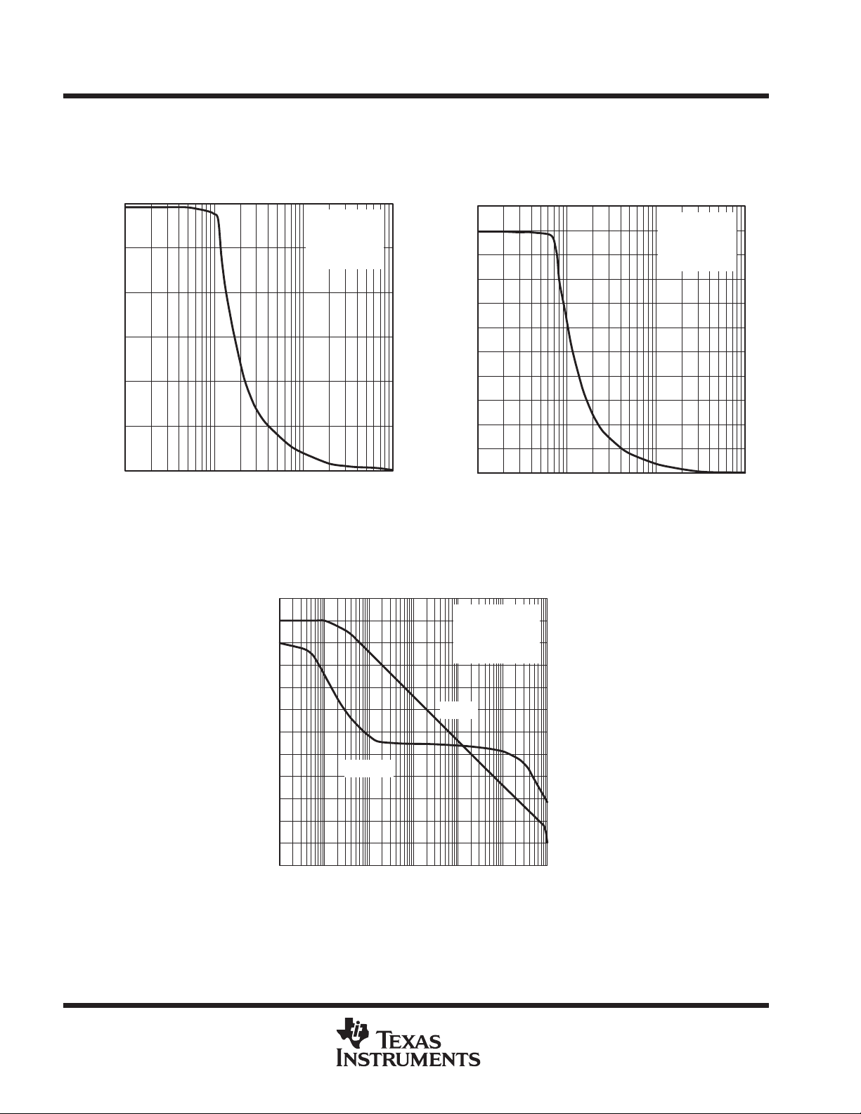
AMPLIFIER WITH A SHUTDOWN PULSE
TURNON CHARACTERISTICS
Shutdown Pin
Amplifier Output
VDD = 5 V
RL = 10 kΩ
AV = 1
TA = 25°C
–3 1
–1 3 9
t – Time – µs
57
Figure 22
SUPPLY CURRENT WITH A SHUTDOWN PULSE
TURNON CHARACTERISTICS
1
Shutdown Pin
AMPLIFIER WITH A SHUTDOWN PULSE
TURNOFF CHARACTERISTICS
5
4
Shutdown Pin
3
2
1
0
Amplifier Output
3
– Shutdown Voltage – V
2
SD
V
1
0
11
–5
–3 1
–1 3
t – Time – µs
VDD = 5 V
RL = 10 kΩ
AV = 1
TA = 25°C
57
Figure 23
5.5
0.8
0.6
0.4
0.2
– Supply Current – mA
DD
I
0
–0.2
–0.4 –0.2 0 0.6
t – Time – µs
Supply Current
VDD = 5 V
VI = 2.5 V
AV = 1
TA = 25°C
Figure 24
4.5
3.5
2.5
1.5
– Shutdown Voltage – V
SD
V
0.5
0.40.2
–0.5
16
POST OFFICE BOX 655303 • DALLAS, TEXAS 75265

TLV2460, TLV2461, TLV2462, TLV2463, TLV2464, TLV2465, TLV246xA
FAMILY OF LOW-POWER RAIL-TO-RAIL INPUT/OUTPUT
OPERATIONAL AMPLIFIERS WITH SHUTDOWN
SLOS220F – JULY 1998 – REVISED OCT OBER 1999
TYPICAL CHARACTERISTICS
TURNOFF SUPPLY CURRENT
WITH A SHUTDOWN PULSE
1
Shutdown Pin
0.8
VDD = 5 V
VI = 2.5 V
AV = 1
TA = 25°C
5.5
4.5
2.5
1.5
0.6
Supply Current
0.4
0.2
– Supply Current – mA
DD
I
0
–0.2
–0.4 –0.2 0 0.6
t – Time – µs
0.40.2
3.5
2.5
1.5
0.5
–0.5
– Shutdown Voltage – V
SD
V
Figure 25
SHUTDOWN SUPPLY CURRENT
vs
FREE-AIR TEMPERATURE
3
2
VDD = 5 V
VI = 2.5 V
1.8
1.75
1.7
1.65
1.6
SR+
SLEW RATE
vs
SUPPLY VOLTAGE
I Supply Current – –Aµ
DD
0.5
–0.5
–1
1
0
–35 5
VDD = 3 V
VI = 1.5 V
–15 25 125–55
TA – Free-Air Temperature – °C
45 65 85 105
Figure 26
POST OFFICE BOX 655303 • DALLAS, TEXAS 75265
1.55
1.5
1.45
SR – Slew Rate – V/µs
1.4
1.35
1.3
2.5 3 3.5 4 5.5 654.5
SR–
V
= 2 V
O(PP)
CL = 160 pF
AV = 1
RL = 10 kΩ
TA = 25°C
VDD – Supply Voltage – V
Figure 27
17

TLV2460, TLV2461, TLV2462, TLV2463, TLV2464, TLV2465, TLV246xA
FAMILY OF LOW-POWER RAIL-TO-RAIL INPUT/OUTPUT
OPERATIONAL AMPLIFIERS WITH SHUTDOWN
SLOS220F – JULY 1998 – REVISED OCT OBER 1999
TYPICAL CHARACTERISTICS
EQUIVALENT INPUT NOISE VOLTAGE
vs
FREQUENCY
18
17
nV/ Hz– Equivalent Input Noise Voltage –V
16
15
14
13
12
11
n
10
100 1k 100k
f – Frequency – Hz
10k
Figure 28
EQUIVALENT INPUT NOISE VOLTAGE
vs
COMMON-MODE INPUT VOLTAGE
20
VDD = 3 V
AV = 10
f = 1 kHz
15
nV/ Hz– Equivalent Input Noise Voltage –V
TA = 25°C
VDD = 3 V
AV = 10
VI = 1.5 V
TA = 25°C
EQUIVALENT INPUT NOISE VOLTAGE
vs
FREQUENCY
18
17
nV/ Hz– Equivalent Input Noise Voltage –V
16
15
14
13
12
11
n
10
100 1k 100k
f – Frequency – Hz
VDD = 5 V
AV = 10
VI = 2.5 V
TA = 25°C
10k
Figure 29
EQUIVALENT INPUT NOISE VOLTAGE
vs
COMMON-MODE INPUT VOLTAGE
20
VDD = 5 V
AV = 10
f = 1 kHz
15
nV/ Hz– Equivalent Input Noise Voltage –V
TA = 25°C
18
14
13
12
11
n
10
0.5 1.5 3
0
V
ICR
1
– Common-Mode Input Voltage – V
2 2.5
Figure 30
POST OFFICE BOX 655303 • DALLAS, TEXAS 75265
14
13
12
11
n
10
0
13
V
– Common-Mode Input Voltage – V
ICR
2
45
Figure 31

TLV2460, TLV2461, TLV2462, TLV2463, TLV2464, TLV2465, TLV246xA
FAMILY OF LOW-POWER RAIL-TO-RAIL INPUT/OUTPUT
OPERATIONAL AMPLIFIERS WITH SHUTDOWN
SLOS220F – JULY 1998 – REVISED OCT OBER 1999
TYPICAL CHARACTERISTICS
TOTAL HARMONIC DISTORTION
vs
FREQUENCY
0.5
VDD = ±1.5 V
V
= 2 V
O(PP)
RL = 10 kΩ
0.1
0.010
THD – Total Harmonic Distortion – %
0.001
100 10k
AV = 100
AV = 10
AV = 1
1k 100k10
f – Frequency – Hz
Figure 32
TOTAL HARMONIC DISTORTION PLUS NOISE
vs
PEAK-TO-PEAK SIGNAL AMPLITUDE
1
VDD = 3 V
AV = 1
TA = 25°C
0.1
RL = 250 Ω
RL = 2 kΩ
RL = 10 kΩ
TOTAL HARMONIC DISTORTION
vs
FREQUENCY
1
VDD = ±2.5 V
V
= 4 V
O(PP)
RL = 10 kΩ
0.1
0.010
THD – Total Harmonic Distortion – %
0.001
AV = 100
AV = 10
AV = 1
100 10k
1k 100k10
f – Frequency – Hz
Figure 33
TOTAL HARMONIC DISTORTION PLUS NOISE
vs
PEAK-TO-PEAK SIGNAL AMPLITUDE
1
RL = 250 Ω
RL = 2 kΩ
0.1
RL = 10 kΩ
0.010
THD+N – Total Harmonic Distortion +Noise – %
0.001
1 1.2 1.4 1.6 2.2 2.421.8 2.6 2.8 3 3.2
Peak-to-Peak Signal Amplitude – V
Figure 34
0.010
RL = 100 kΩ
VDD = 5 V
AV = 1
THD+N – Total Harmonic Distortion +Noise – %
0.001
POST OFFICE BOX 655303 • DALLAS, TEXAS 75265
TA = 25°C
4 4.1 4.2 4.3 4.6 4.74.54.4 4.8 4.9 5
RL = 100 kΩ
Peak-to-Peak Signal Amplitude – V
Figure 35
19

TLV2460, TLV2461, TLV2462, TLV2463, TLV2464, TLV2465, TLV246xA
FAMILY OF LOW-POWER RAIL-TO-RAIL INPUT/OUTPUT
OPERATIONAL AMPLIFIERS WITH SHUTDOWN
SLOS220F – JULY 1998 – REVISED OCT OBER 1999
TYPICAL CHARACTERISTICS
PHASE MARGIN
LOAD CAPACITANCE
90
VDD = ±2.5 V
TA = 25°C
80
RL = 10 kΩ
70
R
= 50 Ω
60
50
40
30
m
20
φ – Phase Margin – degrees
10
0
10 10k
null
100 1k 100k
CL – Load Capacitance – pF
Figure 36
GAIN BANDWIDTH PRODUCT
SUPPLY VOLTAGE
5
CL = 160 pF
RL = 10 kΩ
4.75
f = 10 kHz
TA = 25°C
4.5
vs
vs
PHASE MARGIN
vs
FREE-AIR TEMPERATURE
60
RL = 10 kΩ
CL = 160 pF
55
50
45 65
VDD = ±2.5 V
VDD = ±1.5 V
85 105
45
R
= 20 Ω
null
40
R
null
= 0 Ω
m
φ – Phase Margin – degrees
35
30
–35 5
–15 25 125–55
TA – Free-Air Temperature – °C
Figure 37
GAIN BANDWIDTH PRODUCT
vs
FREE-AIR TEMPERATURE
5
RL = 10 kΩ
CL = 160 pF
4.75
VDD = ±2.5 V
4.5
4.25
4.25
4
Gain Bandwidth Product – MHz
3.75
3.5
2.5 3 3.5 4 5.5 654.5
VDD – Supply Voltage – V
20
Figure 38
4
3.75
VDD = ±1.5 V
3.5
Gain Bandwidth Product – MHz
3.25
3
POST OFFICE BOX 655303 • DALLAS, TEXAS 75265
–35 5
–15 25 125–55
TA – Free-Air Temperature – °C
45 65
Figure 39
85 105

TLV2460, TLV2461, TLV2462, TLV2463, TLV2464, TLV2465, TLV246xA
FAMILY OF LOW-POWER RAIL-TO-RAIL INPUT/OUTPUT
OPERATIONAL AMPLIFIERS WITH SHUTDOWN
SLOS220F – JULY 1998 – REVISED OCT OBER 1999
TYPICAL CHARACTERISTICS
LARGE SIGNAL FOLLOWER
2.2
2
1.8
1.6
1.4
– Voltage – V
O
V
1.2
1
0.8
–2 0 2 4 10
Input
Output
VDD = 3 V
V
I(PP)
VI = 1.5 V
RL = 10 kΩ
CL = 160 pF
AV = 1
TA = 25°C
Figure 40
SMALL SIGNAL FOLLOWER
1.6
= 1 V
Input
Output
861214
t – Time – µs
16 18
LARGE SIGNAL FOLLOWER
3.7
3.3
Input
2.9
2.5
– Voltage – V
O
V
2.1
1.7
1.3
–2 0 2 4 10
VDD = 5 V
V
I(PP)
VI = 2.5 V
RL = 10 kΩ
CL = 160 pF
AV = 1
TA = 25°C
Figure 41
SMALL SIGNAL FOLLOWER
2.6
Output
= 2 V
Input
Output
861214
t – Time – µs
16 18
1.55
Input
1.5
I(PP)
Output
= 100 mV
– Voltage – V
O
V
1.45
1.4
–0.2 0 0.2 0.4 1
VDD = 3 V
V
VI = 1.5 V
RL = 10 kΩ
Figure 42
CL = 160 pF
AV = 1
TA = 25°C
0.80.6 1.2 1.4
t – Time – µs
1.6 1.8
2.55
Input
2.5
I(PP)
Output
= 100 mV
– Voltage – V
O
V
2.45
2.4
–0.2 0 0.2 0.4 1
VDD = 5 V
V
VI = 2.5 V
RL = 10 kΩ
Figure 43
CL = 160 pF
AV = 1
TA = 25°C
0.80.6 1.2 1.4
t – Time – µs
1.6 1.8
POST OFFICE BOX 655303 • DALLAS, TEXAS 75265
21

TLV2460, TLV2461, TLV2462, TLV2463, TLV2464, TLV2465, TLV246xA
FAMILY OF LOW-POWER RAIL-TO-RAIL INPUT/OUTPUT
OPERATIONAL AMPLIFIERS WITH SHUTDOWN
SLOS220F – JULY 1998 – REVISED OCT OBER 1999
TYPICAL CHARACTERISTICS
INVERTING LARGE SIGNAL
2.3
2.1
1.9
1.7
1.5
1.3
– Voltage – V
O
V
1.1
0.9
0.7
0.5
–0.2 0 0.2 0.4 1
Input
VDD = 3 V
V
VI = 1.5 V
RL = 10 kΩ
CL = 160 pF
AV = –1
TA = 25°C
Output
Figure 44
INVERTING SMALL SIGNAL
1.6
= 1 V
I(PP)
0.80.6 1.2 1.4
t – Time – µs
1.6 1.8
INVERTING LARGE SIGNAL
4
3.5
3
2.5
– Voltage – V
O
V
2
1.5
1
–0.2 0 0.2 0.4 1
Input
VDD = 5 V
V
I(PP)
VI = 2.5 V
RL = 10 kΩ
CL = 160 pF
AV = –1
TA = 25°C
Output
Figure 45
INVERTING SMALL SIGNAL
2.6
= 2 V
0.80.6 1.2 1.4
t – Time – µs
1.6 1.8
1.55
1.5
– Voltage – V
O
V
1.45
1.4
–0.2 0 0.2 0.4 1
Figure 46
Input
VDD = 3 V
V
= 100 mV
I(PP)
VI = 1.5 V
RL = 10 kΩ
CL = 160 pF
AV = –1
TA = 25°C
Output
0.80.6 1.2 1.4
t – Time – µs
1.6 1.8
2.55
2.5
– Voltage – V
O
V
2.45
2.4
–0.2 0 0.2 0.4 1
Figure 47
Input
VDD = 5 V
V
= 100 mV
I(PP)
VI = 2.5 V
RL = 10 kΩ
CL = 160 pF
AV = –1
TA = 25°C
Output
0.80.6 1.2 1.4
t – Time – µs
1.6 1.8
22
POST OFFICE BOX 655303 • DALLAS, TEXAS 75265

TLV2460, TLV2461, TLV2462, TLV2463, TLV2464, TLV2465, TLV246xA
FAMILY OF LOW-POWER RAIL-TO-RAIL INPUT/OUTPUT
OPERATIONAL AMPLIFIERS WITH SHUTDOWN
SLOS220F – JULY 1998 – REVISED OCT OBER 1999
PARAMETER MEASUREMENT INFORMATION
_
+
R
null
R
L
C
L
Figure 48
APPLICATION INFORMATION
driving a capacitive load
When the amplifier is configured in this manner, capacitive loading directly on the output will decrease the
device’s phase margin leading to high frequency ringing or oscillations. Therefore, for capacitive loads of greater
than 10 pF, it is recommended that a resistor be placed in series (R
shown in Figure 49. A minimum value of 20 Ω should work well for most applications.
R
F
R
Input
G
_
+
R
NULL
C
) with the output of the amplifier, as
NULL
Output
LOAD
Figure 49. Driving a Capacitive Load
offset voltage
The output offset voltage, (VOO) is the sum of the input offset voltage (VIO) and both input bias currents (IIB) times
the corresponding gains. The following schematic and formula can be used to calculate the output offset
voltage:
R
F
I
VOO+
R
G
R
S
V
ǒ
IO
Figure 50. Output Offset Voltage Model
1
) ǒ
R
R
IB–
I
IB+
+
V
I
F
Ǔ
"
I
Ǔ
IB
G
)
–
+
R
1
) ǒ
F
Ǔ
R
G
R
ǒ
S
V
O
"
I
Ǔ
IB–RF
POST OFFICE BOX 655303 • DALLAS, TEXAS 75265
23

TLV2460, TLV2461, TLV2462, TLV2463, TLV2464, TLV2465, TLV246xA
FAMILY OF LOW-POWER RAIL-TO-RAIL INPUT/OUTPUT
OPERATIONAL AMPLIFIERS WITH SHUTDOWN
SLOS220F – JULY 1998 – REVISED OCT OBER 1999
APPLICATION INFORMATION
general configurations
When receiving low-level signals, limiting the bandwidth of the incoming signals into the system is often
required. The simplest way to accomplish this is to place an RC filter at the noninverting terminal of the amplifer
(see Figure 51).
R
G
R
F
–
R
R
C1
F
G
+
ǒ
Ǔ
1)sR1C1
f
1
–3dB
Ǔ
V
I
R1
V
O
+ ǒ
1
V
I
)
+
2pR1C1
V
O
1
Figure 51. Single-Pole Low-Pass Filter
If even more attenuation is needed, a multiple pole filter is required. The Sallen-Key filter can be used for this
task. For best results, the amplifier should have a bandwidth that is 8 to 10 times the filter frequency bandwidth.
Failure to do this can result in phase shift of the amplifier.
C1
V
I
R2R1
C2
R
G
+
_
R
F
R1 = R2 = R
C1 = C2 = C
Q = Peaking Factor
(Butterworth Q = 0.707)
1
+
2pRC
R
F
1
2 –
(
)
Q
R
f
–3dB
G
=
24
Figure 52. 2-Pole Low-Pass Sallen-Key Filter
POST OFFICE BOX 655303 • DALLAS, TEXAS 75265

TLV2460, TLV2461, TLV2462, TLV2463, TLV2464, TLV2465, TLV246xA
FAMILY OF LOW-POWER RAIL-TO-RAIL INPUT/OUTPUT
OPERATIONAL AMPLIFIERS WITH SHUTDOWN
SLOS220F – JULY 1998 – REVISED OCT OBER 1999
APPLICATION INFORMATION
shutdown function
Three members of the TLV246x family (TLV2460/3/5) have a shutdown terminal for conserving battery life in
portable applications. When the shutdown terminal is tied low, the supply current is reduced to 0.3 µA/channel,
the amplifier is disabled, and the outputs are placed in a high impedance mode. To enable the amplifier, the
shutdown terminal can either be left floating or pulled high. When the shutdown terminal is left floating, care
should be taken to ensure that parasitic leakage current at the shutdown terminal does not inadvertently place
the operational amplifier into shutdown. The shutdown terminal threshold is always referenced to V
Therefore, when operating the device with split supply voltages (e.g. ±2.5 V), the shutdown terminal needs to
be pulled to V
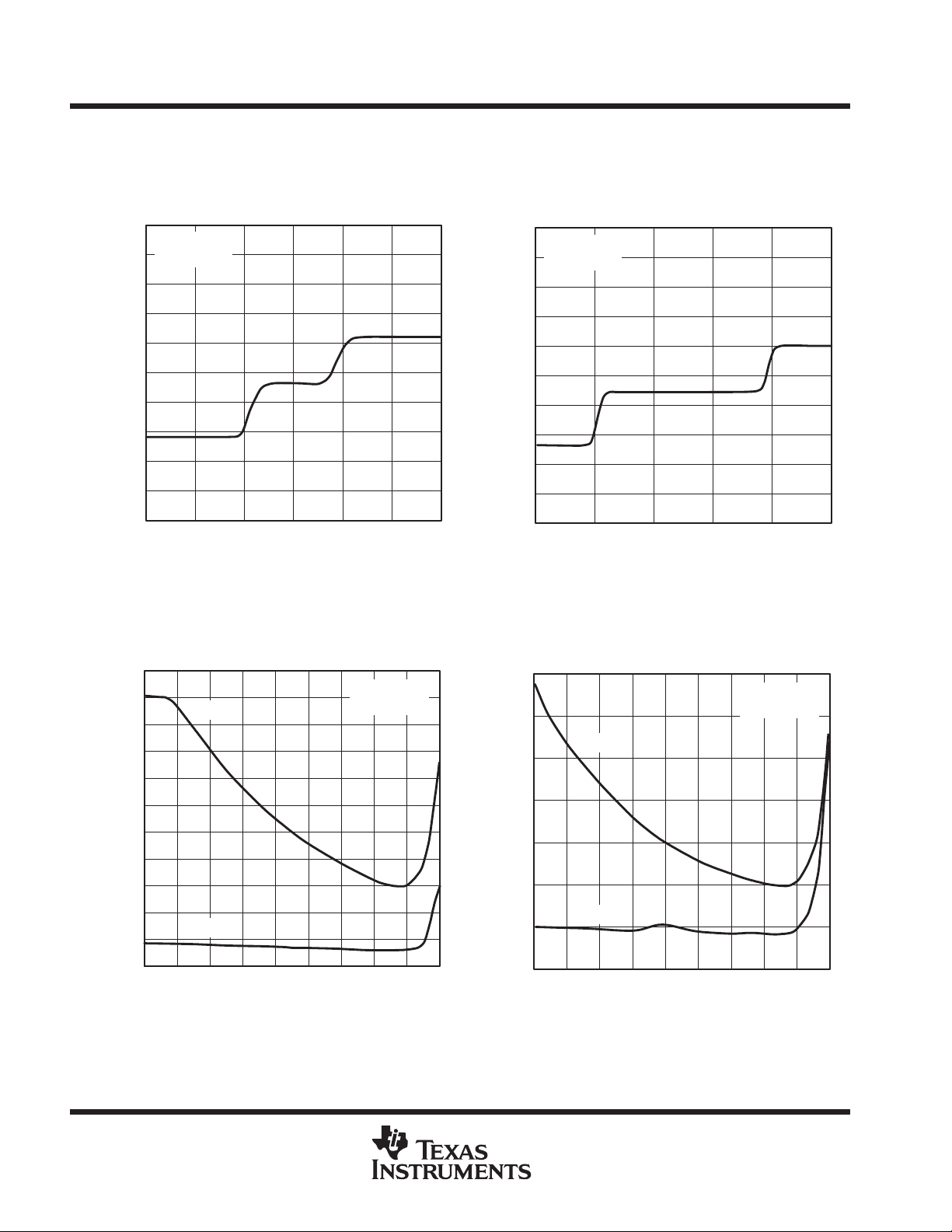
The amplifier’s output with a shutdown pulse is shown in Figures 22, 23, 24, and 25. The amplifier is powered
with a single 5-V supply and configured as a noninverting configuration with a gain of 5. The amplifier turnon
and turnoff times are measured from the 50% point of the shutdown pulse to the 50% point of the output
waveform. The times for the single, dual, and quad are listed in the data tables.
circuit layout considerations
T o achieve the levels of high performance of the TL V246x, follow proper printed-circuit board design techniques.
A general set of guidelines is given in the following.
– (not GND) to disable the operational amplifier.
DD
DD
/2.
D
Ground planes – It is highly recommended that a ground plane be used on the board to provide all
components with a low inductive ground connection. However, in the areas of the amplifier inputs and
output, the ground plane can be removed to minimize the stray capacitance.
D
Proper power supply decoupling – Use a 6.8-µF tantalum capacitor in parallel with a 0.1-µF ceramic
capacitor on each supply terminal. It may be possible to share the tantalum among several amplifiers
depending on the application, but a 0.1-µF ceramic capacitor should always be used on the supply terminal
of every amplifier. In addition, the 0.1-µF capacitor should be placed as close as possible to the supply
terminal. As this distance increases, the inductance in the connecting trace makes the capacitor less
effective. The designer should strive for distances of less than 0.1 inches between the device power
terminals and the ceramic capacitors.
D
Sockets – Sockets can be used but are not recommended. The additional lead inductance in the socket pins
will often lead to stability problems. Surface-mount packages soldered directly to the printed-circuit board
is the best implementation.
D
Short trace runs/compact part placements – Optimum high performance is achieved when stray series
inductance has been minimized. To realize this, the circuit layout should be made as compact as possible,
thereby minimizing the length of all trace runs. Particular attention should be paid to the inverting input of
the amplifier. Its length should be kept as short as possible. This will help to minimize stray capacitance at
the input of the amplifier.
D
Surface-mount passive components – Using surface-mount passive components is recommended for high
performance amplifier circuits for several reasons. First, because of the extremely low lead inductance of
surface-mount components, the problem with stray series inductance is greatly reduced. Second, the small
size of surface-mount components naturally leads to a more compact layout thereby minimizing both stray
inductance and capacitance. If leaded components are used, it is recommended that the lead lengths be
kept as short as possible.
POST OFFICE BOX 655303 • DALLAS, TEXAS 75265
25
TLV2460, TLV2461, TLV2462, TLV2463, TLV2464, TLV2465, TLV246xA
FAMILY OF LOW-POWER RAIL-TO-RAIL INPUT/OUTPUT
OPERATIONAL AMPLIFIERS WITH SHUTDOWN
SLOS220F – JULY 1998 – REVISED OCT OBER 1999
APPLICATION INFORMATION
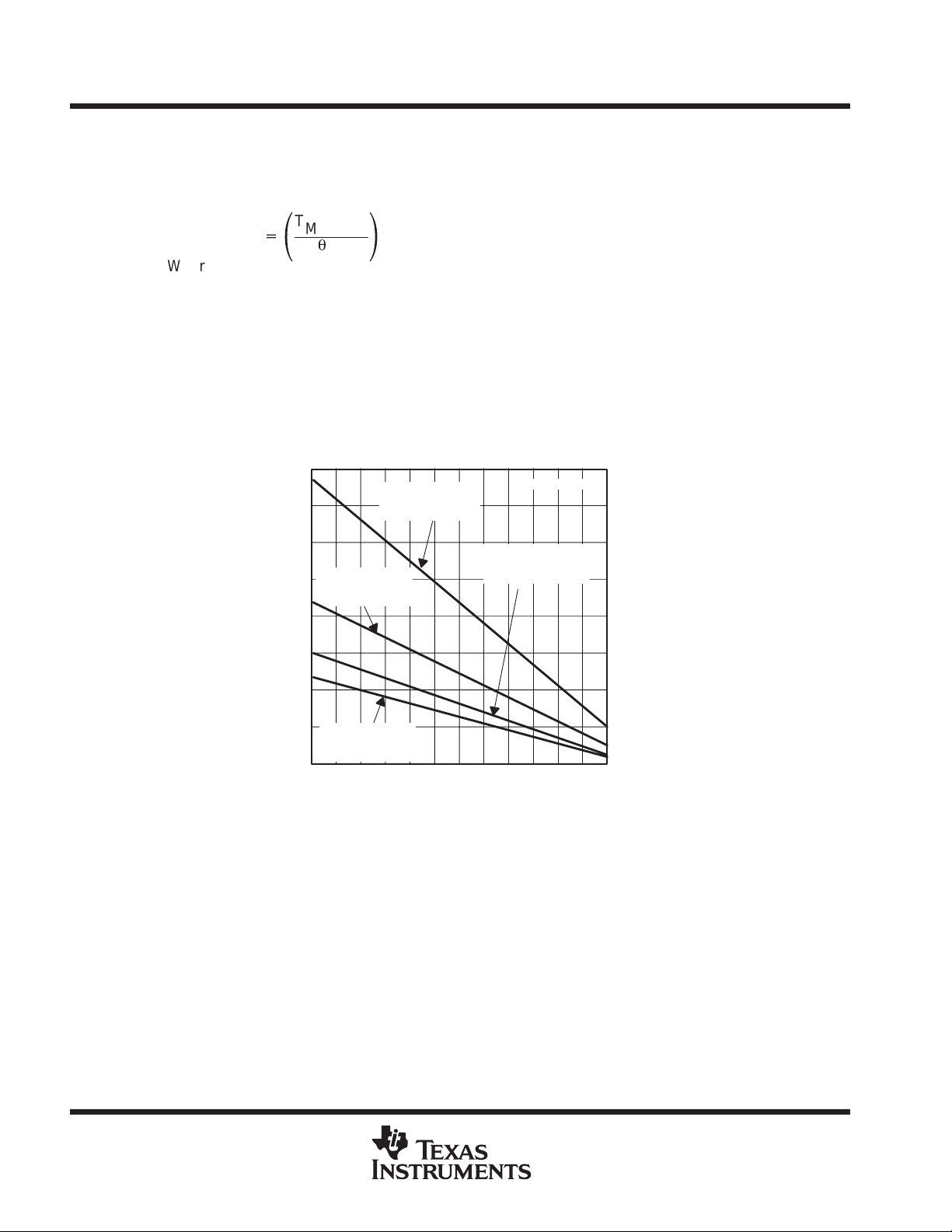
general power dissipation considerations
For a given θJA, the maximum power dissipation is shown in Figure 53 and is calculated by the following formula:
T
MAX–TA
Where:
ǒ
PD+
P
= Maximum power dissipation of THS246x IC (watts)
D
T
= Absolute maximum junction temperature (150°C)
MAX
T
= Free-ambient air temperature (°C)
A
θ
= θ
JA
JC
+ θ
q
θJC= Thermal coefficient from junction to case
θCA= Thermal coefficient from case to ambient air (°C/W)
2
1.75
Ǔ
JA
CA
MAXIMUM POWER DISSIPATION
vs
FREE-AIR TEMPERATURE
PDIP Package
Low-K Test PCB
θJA = 104°C/W
TJ = 150°C
1.5
SOIC Package
1.25
Low-K Test PCB
θJA = 176°C/W
1
0.75
0.5
Maximum Power Dissipation – W
SOT-23 Package
0.25
Low-K Test PCB
θJA = 324°C/W
0
–55–40 –25 –10 5
TA – Free-Air Temperature – °C
NOTE A: Results are with no air flow and using JEDEC Standard Low-K test PCB.
20 35 50
MSOP Package
Low-K Test PCB
θJA = 260°C/W
65 80 95 110 125
Figure 53. Maximum Power Dissipation vs Free-Air Temperature
26
POST OFFICE BOX 655303 • DALLAS, TEXAS 75265

macromodel information
TLV2460, TLV2461, TLV2462, TLV2463, TLV2464, TLV2465, TLV246xA
FAMILY OF LOW-POWER RAIL-TO-RAIL INPUT/OUTPUT
OPERATIONAL AMPLIFIERS WITH SHUTDOWN
SLOS220F – JULY 1998 – REVISED OCT OBER 1999
APPLICATION INFORMATION
Macromodel information provided was derived using Microsim
software used with Microsim
PSpice
. The Boyle macromodel (see Note 2) and subcircuit in Figure 54 are
generated using the TLV246x typical electrical and operating characteristics at T
Parts
Release 8, the model generation
= 25°C. Using this
A
information, output simulations of the following key parameters can be generated to a tolerance of 20% (in most
cases):
D
Maximum positive output voltage swing
D
Maximum negative output voltage swing
D
Slew rate
D
Quiescent power dissipation
D
Input bias current
D
Open-loop voltage amplification
NOTE 2: G. R. Boyle, B. M. Cohn, D. O. Pederson, and J. E. Solomon, “Macromodeling of Intergrated Circuit Operational Amplifiers”,
V
GND
Journal of Solid-State Circuits,
3
DD+
RP
2
IN –
IN+
1
DP
4
ISS
SC-9, 353 (1974).
RSS
10
J1 J2
11
C1
RD1
CSS
12
RD2
+
VD
–
DC
DE
+
VE
–
53
54
D
Unity-gain frequency
D
Common-mode rejection ratio
D
Phase margin
D
DC output resistance
D
AC output resistance
D
Short-circuit output current limit
EGND
R2 6
9
+
VB
–
90
HLIM
+
–
GCM
+
DLP
–
+
–
91
C2
GA
DLN
FB
99
RO2
7
+
VLIM
92
–
VLNVLP
+
–
8
RO1
5
IEEE
OUT
.SUBCKT TLV246X 1 2 3 4 5
PSpice
C1 11 12 2.46034E–12
C2 6 7 10.0000E–12
CSS 10 99 443.21E–15
DC 5 53 DY
DE 54 5 DY
DLP 90 91 DX
DLN 92 90 DX
DP 43DX
EGND 99 0 POLY (2) (3,0) (4,0) 0 .5 .5
FB 7 99 POLY (5) VB VC VE VLP
+ VLN 0 21.600E6 –1E3 1E3 22E6 –22E6
GA 6 0 11 12 345.26E–6
GCM 0 6 10 99 15.4226E–9
ISS 10 4 DC 18.850E–6
HLIM 90 0 VLIM 1K
J1 11 2 10 JX1
J2 12 1 10 JX2
R2 6 9 100.00E3
and
Parts
are trademarks of MicroSim Corporation.
RD1 3 11 2.8964E3
RD2 3 12 2.8964E3
R01 8 5 5.6000
R02 7 99 6.2000
RP 3 4 8.9127
RSS 10 99 10.610E6
VB 9 0 DC 0
VC 3 53 DC .7836
VE 54 4 DC .7436
VLIM 7 8 DC 0
VLP 91 0 DC 117
VLN 0 92 DC 117
.MODEL DX D (IS=800.00E–18)
.MODEL DY D (IS=800.00E–18 Rs = 1m Cjo=10p)
.MODEL JX1 NJF (IS=1.0000E–12 BETA=6.3239E–3
+ VTO=–1)
.MODEL JX2 NJF (IS=1.0000E–12 BETA=6.3239E–3
+ VTO=–1)
.ENDS
Figure 54. Boyle Macromodels and Subcircuit
POST OFFICE BOX 655303 • DALLAS, TEXAS 75265
27

TLV2460, TLV2461, TLV2462, TLV2463, TLV2464, TLV2465, TLV246xA
FAMILY OF LOW-POWER RAIL-TO-RAIL INPUT/OUTPUT
OPERATIONAL AMPLIFIERS WITH SHUTDOWN
SLOS220F – JULY 1998 – REVISED OCT OBER 1999
macromodel information (continued)
.subckt TLV_246Y 1 2 3 4 5 6
21.600E6 –1E3 1E3 22E6 –22E6
c1 11 12 2.4603E–12
c2 72 7 10.000E–12
css 10 99 443.21E–15
dc 70 53 dy
de 54 70 dy
dlp 90 91 dx
dln 92 90 dx
dp 4 3 dx
egnd 99 0 poly(2) (3,0) (4,0) 0 .5 .5
fb 7 99 poly(5) vb vc ve vlp vln 0
ga 72 0 11 12 345.26E–6
gcm 0 72 10 99 15.422E–9
iss 74 4 dc 18.850E–6
hlim 90 0 vlim 1K
j1 11 2 10 jx1
j2 12 1 10 jx2
r2 72 9 100.00E3
rd1 3 11 2.8964E3
rd2 3 12 2.8964E3
ro1 8 70 5.6000
ro2 7 99 6.2000
Figure 54. Boyle Macromodels and Subcircuit (Continued)
rp 3 71 8.9127
rss 10 99 10.610E6
rs1 6 4 1G
rs2 6 4 1G
rs3 6 4 1G
rs4 6 4 1G
s1 71 4 6 4 s1x
s2 70 5 6 4 s1x
s3 10 74 6 4 s1x
s4 74 4 6 4 s2x
vb 9 0 dc 0
vc 3 53 dc .7836
ve 54 4 dc .7436
vlim 7 8 dc 0
vlp 91 0 dc 117
vln 0 92 dc 117
.model dx D(Is=800.00E–18)
.model dy D(Is=800.00E–18 Rs=1m Cjo=10p)
.model jx1 NJF(Is=1.0000E–12 Beta=6.3239E–3 Vto=–1)
.model jx2 NJF(Is=1.0000E–12 Beta=6.3239E–3 Vto=–1)
.model s1x VSWITCH(Roff=1E8 Ron=1.0 Voff=2.5 Von=0.0)
.model s2x VSWITCH(Roff=1E8 Ron=1.0 V off=0 Von=2.5)
.ends
28
POST OFFICE BOX 655303 • DALLAS, TEXAS 75265
TLV2460, TLV2461, TLV2462, TLV2463, TLV2464, TLV2465, TLV246xA
FAMILY OF LOW-POWER RAIL-TO-RAIL INPUT/OUTPUT
OPERATIONAL AMPLIFIERS WITH SHUTDOWN
SLOS220F – JULY 1998 – REVISED OCT OBER 1999
MECHANICAL DATA
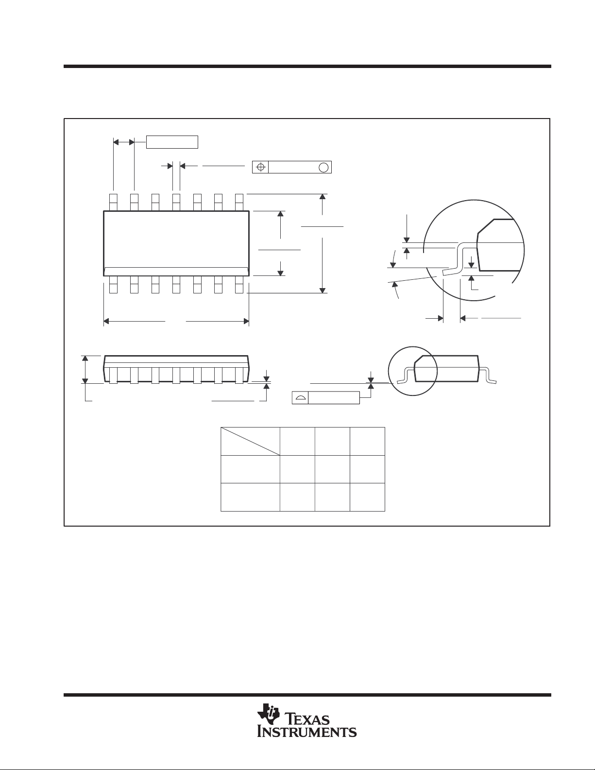
D (R-PDSO-G**) PLASTIC SMALL-OUTLINE PACKAGE
14 PIN SHOWN
0.050 (1,27)
14
1
0.069 (1,75) MAX
A
0.020 (0,51)
0.014 (0,35)
0.010 (0,25)
0.004 (0,10)
DIM
8
7
PINS **
0.010 (0,25)
0.157 (4,00)
0.150 (3,81)
M
0.244 (6,20)
0.228 (5,80)
Seating Plane
0.004 (0,10)
8
14
0.008 (0,20) NOM
0°–8°
16
Gage Plane
0.010 (0,25)
0.044 (1,12)
0.016 (0,40)
A MAX
A MIN
NOTES: B. All linear dimensions are in inches (millimeters).
C. This drawing is subject to change without notice.
D. Body dimensions do not include mold flash or protrusion, not to exceed 0.006 (0,15).
E. Falls within JEDEC MS-012
POST OFFICE BOX 655303 • DALLAS, TEXAS 75265
0.197
(5,00)
0.189
(4,80)
0.344
(8,75)
0.337
(8,55)
0.394
(10,00)
0.386
(9,80)
4040047/D 10/96
29

TLV2460, TLV2461, TLV2462, TLV2463, TLV2464, TLV2465, TLV246xA
FAMILY OF LOW-POWER RAIL-TO-RAIL INPUT/OUTPUT
OPERATIONAL AMPLIFIERS WITH SHUTDOWN
SLOS220F – JULY 1998 – REVISED OCT OBER 1999
MECHANICAL DATA
DBV (R-PDSO-G5) PLASTIC SMALL-OUTLINE PACKAGE
0,95
1,30
1,00
0,40
0,20
45
1,80
1,50
1
3,10
2,70
3
0,05 MIN
M
0,25
3,00
2,50
Seating Plane
0,10
0,15 NOM
0°–8°
Gage Plane
0,25
0,55
0,35
NOTES: A. All linear dimensions are in millimeters.
B. This drawing is subject to change without notice.
C. Body dimensions include mold flash or protrusion.
4073253-4/B 10/97
30
POST OFFICE BOX 655303 • DALLAS, TEXAS 75265

TLV2460, TLV2461, TLV2462, TLV2463, TLV2464, TLV2465, TLV246xA
FAMILY OF LOW-POWER RAIL-TO-RAIL INPUT/OUTPUT
OPERATIONAL AMPLIFIERS WITH SHUTDOWN
SLOS220F – JULY 1998 – REVISED OCT OBER 1999
MECHANICAL DATA
DBV (R-PDSO-G6) PLASTIC SMALL-OUTLINE PACKAGE
0,95
1,30
1,00
0,40
0,20
46
1,80
1,50
1
3,10
2,70
3
0,05 MIN
M
0,25
3,00
2,50
Seating Plane
0,15 NOM
Gage Plane
0,25
0°–8°
0,10
NOTES: A. All linear dimensions are in millimeters.
B. This drawing is subject to change without notice.
C. Body dimensions include mold flash or protrusion.
4073253-5/B 10/97
POST OFFICE BOX 655303 • DALLAS, TEXAS 75265
31

TLV2460, TLV2461, TLV2462, TLV2463, TLV2464, TLV2465, TLV246xA
FAMILY OF LOW-POWER RAIL-TO-RAIL INPUT/OUTPUT
OPERATIONAL AMPLIFIERS WITH SHUTDOWN
SLOS220F – JULY 1998 – REVISED OCT OBER 1999
MECHANICAL DATA
DGK (R-PDSO-G8) PLASTIC SMALL-OUTLINE PACKAGE
0,65
0,38
0,25
8
1
3,05
2,95
5
3,05
2,95
4
Seating Plane
0,25
4,98
4,78
M
0,15 NOM
Gage Plane
0,25
0°–6°
0,69
0,41
1,07 MAX
NOTES: A. All linear dimensions are in millimeters.
B. This drawing is subject to change without notice.
C. Body dimensions do not include mold flash or protrusion.
D. Falls within JEDEC MO-187
0,15 MIN
0,10
4073329/A 02/97
32
POST OFFICE BOX 655303 • DALLAS, TEXAS 75265

TLV2460, TLV2461, TLV2462, TLV2463, TLV2464, TLV2465, TLV246xA
FAMILY OF LOW-POWER RAIL-TO-RAIL INPUT/OUTPUT
OPERATIONAL AMPLIFIERS WITH SHUTDOWN
SLOS220F – JULY 1998 – REVISED OCT OBER 1999
MECHANICAL DATA
DGS (S-PDSO-G10) PLASTIC SMALL-OUTLINE PACKAGE
0,50
10
1
1,07 MAX
3,05
2,95
0,27
0,17
6
3,05
2,95
5
Seating Plane
0,15
0,05
0,25
4,98
4,78
M
0,10
0,15 NOM
Gage Plane
0°–6°
0,25
0,69
0,41
NOTES: A. All linear dimensions are in millimeters.
B. This drawing is subject to change without notice.
C. Body dimensions do not include mold flash or protrusion.
4073272/A 12/97
POST OFFICE BOX 655303 • DALLAS, TEXAS 75265
33

TLV2460, TLV2461, TLV2462, TLV2463, TLV2464, TLV2465, TLV246xA
FAMILY OF LOW-POWER RAIL-TO-RAIL INPUT/OUTPUT
OPERATIONAL AMPLIFIERS WITH SHUTDOWN
SLOS220F – JULY 1998 – REVISED OCT OBER 1999
MECHANICAL DATA
N (R-PDIP-T**) PLASTIC DUAL-IN-LINE PACKAGE
16 PIN SHOWN
16
1
0.035 (0,89) MAX
PINS **
DIM
A
9
0.260 (6,60)
0.240 (6,10)
8
0.070 (1,78) MAX
0.020 (0,51) MIN
0.200 (5,08) MAX
A MAX
A MIN
Seating Plane
14
0.775
(19,69)
0.745
(18,92)
16
0.775
(19,69)
0.745
(18,92)
18
0.920
(23.37)
0.850
(21.59)
0.310 (7,87)
0.290 (7,37)
20
0.975
(24,77)
0.940
(23,88)
0.100 (2,54)
0.021 (0,53)
0.015 (0,38)
NOTES: A. All linear dimensions are in inches (millimeters).
B. This drawing is subject to change without notice.
C. Falls within JEDEC MS-001 (20 pin package is shorter then MS-001.)
0.010 (0,25)
M
0.125 (3,18) MIN
0°–15°
0.010 (0,25) NOM
14/18 PIN ONL Y
4040049/C 08/95
34
POST OFFICE BOX 655303 • DALLAS, TEXAS 75265

TLV2460, TLV2461, TLV2462, TLV2463, TLV2464, TLV2465, TLV246xA
FAMILY OF LOW-POWER RAIL-TO-RAIL INPUT/OUTPUT
OPERATIONAL AMPLIFIERS WITH SHUTDOWN
SLOS220F – JULY 1998 – REVISED OCT OBER 1999
MECHANICAL DATA
P (R-PDIP-T8) PLASTIC DUAL-IN-LINE PACKAGE
0.400 (10,60)
0.355 (9,02)
58
0.260 (6,60)
0.240 (6,10)
41
0.070 (1,78) MAX
0.020 (0,51) MIN
0.200 (5,08) MAX
0.125 (3,18) MIN
0.100 (2,54)
0.021 (0,53)
0.015 (0,38)
NOTES: A. All linear dimensions are in inches (millimeters).
B. This drawing is subject to change without notice.
C. Falls within JEDEC MS-001
0.010 (0,25)
M
0.310 (7,87)
0.290 (7,37)
Seating Plane
0°–15°
0.010 (0,25) NOM
4040082/B 03/95
POST OFFICE BOX 655303 • DALLAS, TEXAS 75265
35

TLV2460, TLV2461, TLV2462, TLV2463, TLV2464, TLV2465, TLV246xA
FAMILY OF LOW-POWER RAIL-TO-RAIL INPUT/OUTPUT
OPERATIONAL AMPLIFIERS WITH SHUTDOWN
SLOS220F – JULY 1998 – REVISED OCT OBER 1999
MECHANICAL DATA
PW (R-PDSO-G**) PLASTIC SMALL-OUTLINE PACKAGE
14 PIN SHOWN
0,65
14
1
1,20 MAX
0,30
0,19
8
4,50
4,30
7
A
0,15
0,05
6,60
6,20
M
0,10
Seating Plane
0,10
0,15 NOM
Gage Plane
0,25
0°–8°
0,75
0,50
PINS **
DIM
A MAX
A MIN
NOTES: A. All linear dimensions are in millimeters.
B. This drawing is subject to change without notice.
C. Body dimensions do not include mold flash or protrusion not to exceed 0,15.
D. Falls within JEDEC MO-153
8
3,10
2,90
14
5,10
4,90
16
5,10
20
6,60
6,404,90
24
7,90
7,70
28
9,80
9,60
4040064/E 08/96
36
POST OFFICE BOX 655303 • DALLAS, TEXAS 75265

IMPORTANT NOTICE
T exas Instruments and its subsidiaries (TI) reserve the right to make changes to their products or to discontinue
any product or service without notice, and advise customers to obtain the latest version of relevant information
to verify, before placing orders, that information being relied on is current and complete. All products are sold
subject to the terms and conditions of sale supplied at the time of order acknowledgement, including those
pertaining to warranty, patent infringement, and limitation of liability.
TI warrants performance of its semiconductor products to the specifications applicable at the time of sale in
accordance with TI’s standard warranty. Testing and other quality control techniques are utilized to the extent
TI deems necessary to support this warranty . Specific testing of all parameters of each device is not necessarily
performed, except those mandated by government requirements.
CERTAIN APPLICA TIONS USING SEMICONDUCT OR PRODUCTS MAY INVOLVE POTENTIAL RISKS OF
DEATH, PERSONAL INJURY, OR SEVERE PROPERTY OR ENVIRONMENTAL DAMAGE (“CRITICAL
APPLICATIONS”). TI SEMICONDUCTOR PRODUCTS ARE NOT DESIGNED, AUTHORIZED, OR
WARRANTED TO BE SUITABLE FOR USE IN LIFE-SUPPORT DEVICES OR SYSTEMS OR OTHER
CRITICAL APPLICA TIONS. INCLUSION OF TI PRODUCTS IN SUCH APPLICATIONS IS UNDERST OOD TO
BE FULLY AT THE CUSTOMER’S RISK.
In order to minimize risks associated with the customer’s applications, adequate design and operating
safeguards must be provided by the customer to minimize inherent or procedural hazards.
TI assumes no liability for applications assistance or customer product design. TI does not warrant or represent
that any license, either express or implied, is granted under any patent right, copyright, mask work right, or other
intellectual property right of TI covering or relating to any combination, machine, or process in which such
semiconductor products or services might be or are used. TI’s publication of information regarding any third
party’s products or services does not constitute TI’s approval, warranty or endorsement thereof.
Copyright 1999, Texas Instruments Incorporated
 Loading...