

Datasheet TLV2404IPWR, TLV2404IPW, TLV2404IN, TLV2404IDR, TLV2404ID Datasheet (Texas Instruments)
...
TLV2401, TLV2402, TLV2404
FAMILY OF 900-nA/Ch RAIL-TO-RAIL INPUT/OUTPUT
OPERATIONAL AMPLIFIERS WITH REVERSE BATTERY PROTECTION
SLOS244 – FEBRUARY 2000
1
POST OFFICE BOX 655303 • DALLAS, TEXAS 75265
D
Micro-Power Operation ... < 1 µA/Channel
D
Input Common-Mode Range Exceeds the
Rails ... –0.1 V to VCC + 5 V
D
Rail-to-Rail Input/Output
D
Gain Bandwidth Product ... 5.5 kHz
D
Supply Voltage Range ... 2.5 V to 16 V
D
Specified Temperature Range
– TA = 0°C to 70°C... Commercial Grade
– TA = –40°C to 125°C... Industrial Grade
D
Ultra-Small Packaging
– 5-Pin SOT-23 (TLV2401)
– 8-Pin MSOP (TLV2402)
D
Universal OpAmp EVM
description
The TLV240x family of single-supply operational
amplifiers has the lowest supply current available
today at only 900 nA per channel. Added to this is
reverse battery protection making the device even
more ideal for battery powered systems. And for
harsh environments, the inputs can be taken 5 V
above the positive supply rail without damage to
the device.
The low supply current is coupled with extremely
low input bias currents enabling them to be used
with mega-Ω resistors making them ideal for
portable, long active life, applications. DC
accuracy is ensured with a low typical offset
voltage as low as 390 µV, CMRR of 120 dB and
minimum open loop gain of 130 V/mV at 2.7 V.
The maximum recommended supply voltage is as high as 16 V and ensured operation down to 2.5 V, with
electrical characteristics specified at 2.7 V, 5 V and 15 V. The 2.5-V operation makes it compatible with Li-Ion
battery-powered systems and many micro-power microcontrollers available today including TI’s MSP430.
All members are available in PDIP and SOIC with the singles in the small SOT-23 package, duals in the MSOP,
and quads in TSSOP.
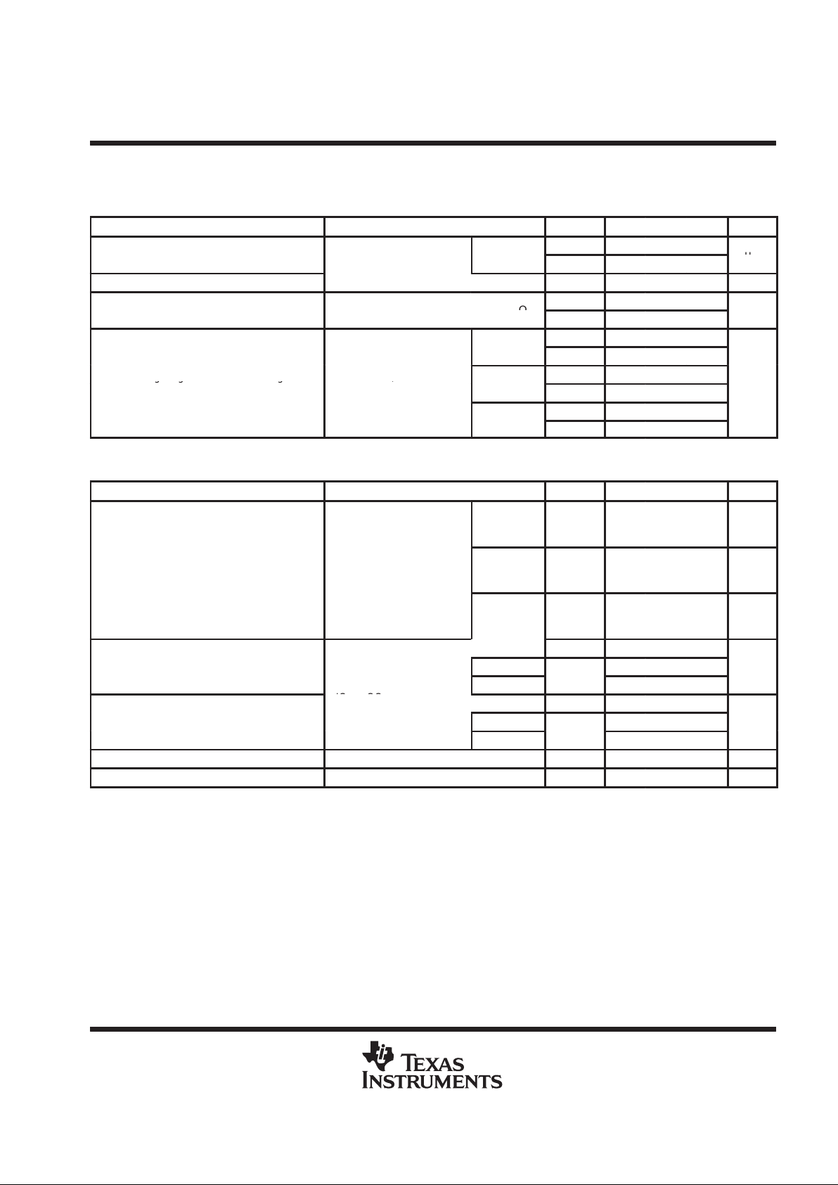
FAMILY PACKAGE TABLE
PACKAGE TYPES
UNIVERSAL
DEVICE
NO. OF Ch
PDIP SOIC SOT-23 TSSOP MSOP
EVM
TLV2401
†
1 8 8 5 — —
TLV2402
†
2 8 8 — — 8
Refer to the EVM
Selection Guide
TLV2404 4 14 14 — 14 —
(Lit# SLOU060)
†
This device is in the Product Preview stage of development. Contact your local TI slaes office for more
information
1
2
3
4
5
6
7
14
13
12
11
10
9
8
1OUT
1IN–
1IN+
V
CC
2IN+
2IN–
2OUT
4OUT
4IN–
4IN+
GND
3IN+
3IN–
3OUT
(TOP VIEW)
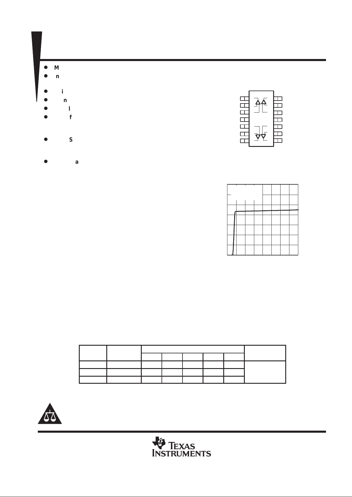
TLV2404
D, N, OR PW PACKAGE
0
0.2
0.4
0.6
0.8
1.0
1.2
1.4
0246810121416
SUPPLY CURRENT
vs
SUPPLY VOLTAGE
VCC – Supply Voltage – V
CC
I Supply Current – – A/Chµ
AV = 1
VIN = VCC / 2
TA =25 °C
Copyright 2000, Texas Instruments Incorporated
PRODUCTION DATA information is current as of publication date.
Products conform to specifications per the terms of Texas Instruments
standard warranty. Production processing does not necessarily include
testing of all parameters.
Please be aware that an important notice concerning availability, standard warranty, and use in critical applications of
Texas Instruments semiconductor products and disclaimers thereto appears at the end of this data sheet.
TI is a trademark of Texas Instruments Incorporated.
TLV2401, TLV2402, TLV2404
FAMILY OF 900-nA/Ch RAIL-TO-RAIL INPUT/OUTPUT
OPERATIONAL AMPLIFIERS WITH REVERSE BATTERY PROTECTION
SLOS244 – FEBRUARY 2000
2
POST OFFICE BOX 655303 • DALLAS, TEXAS 75265
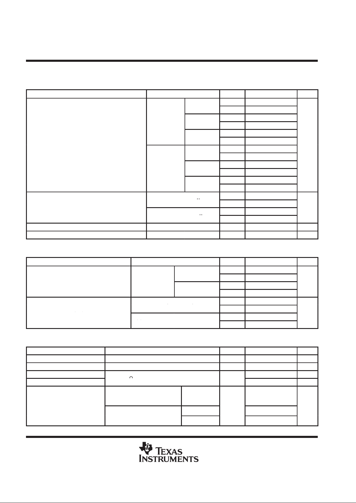
TLV2401 AVAILABLE OPTIONS
PACKAGED DEVICES
T
A
V
IO
max
AT 25°C
SMALL OUTLINE
(D)
SOT-23
†
(DBV)
PLASTIC DIP
(P)
0°C to 70°C
TLV2401CD TLV2401CDBV TLV2401CP
-40°C to 125°C
1500 µV
TLV2401ID TLV2401IDBV TLV2401IP
†
This package is available taped and reeled. To order this packaging option, add an R suffix to the part
number (e.g., TL V2401CDR).
TLV2402 AVAILABLE OPTIONS
PACKAGED DEVICES
T
A
V
IO
max
AT 25°C
SMALL OUTLINE
†
(D)
MSOP
(DGK)
PLASTIC DIP
(P)
0°C to 70°C
TLV2402CD TLV2402CDGK TLV2402CP
–40°C to 125°C
1500 µV
TLV2402ID TLV2402IDGK TLV2402IP
†
This package is available taped and reeled. To order this packaging option, add an R suffix to the part
number (e.g., TL V2402CDR).
TLV2404 AVAILABLE OPTIONS
PACKAGED DEVICES
T
A
V
IO
max
AT 25°C
SMALL OUTLINE
(D)
PLASTIC DIP
(N)
TSSOP
(PW)
0°C to 70°C
TLV2404CD TLV2404CN TLV2404CPW
–40°C to 125°C
1500 µV
TLV2404ID TLV2404IN TLV2404IPW
†
This package is available taped and reeled. To order this packaging option, add an R suffix to the part
number (e.g., TL V2404CDR).
TLV2401, TLV2402, TLV2404
FAMILY OF 900-nA/Ch RAIL-TO-RAIL INPUT/OUTPUT
OPERATIONAL AMPLIFIERS WITH REVERSE BATTERY PROTECTION
SLOS244 – FEBRUARY 2000
3
POST OFFICE BOX 655303 • DALLAS, TEXAS 75265
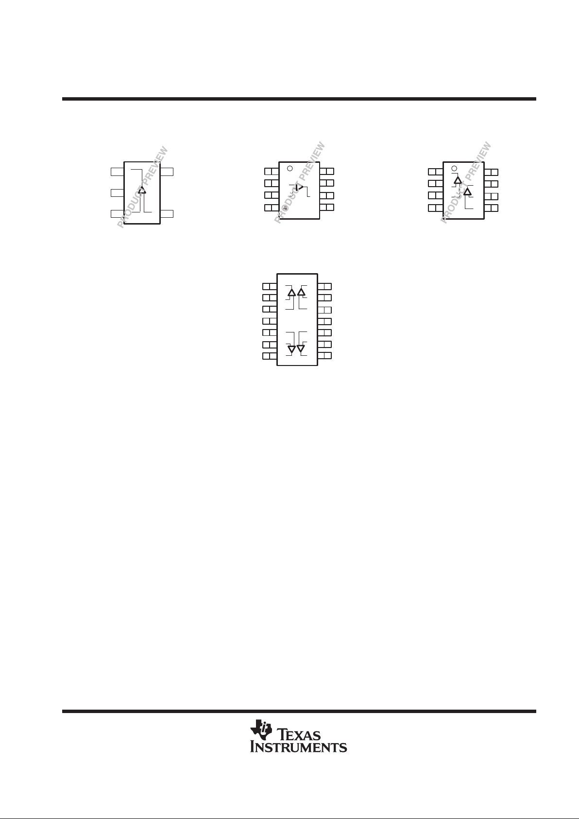
TLV240x P ACKAGE PINOUTS
3
2
4
5
(TOP VIEW)
1
OUT
GND
IN+
V
CC
IN–
TLV2401
DBV PACKAGE
NC – No internal connection
1
2
3
4
8
7
6
5
NC
IN–
IN+
GND
NC
V
CC
OUT
NC
TLV2401
D OR P PACKAGE
(TOP VIEW)
1
2
3
4
8
7
6
5
1OUT
1IN–
1IN+
GND
V
CC
2OUT
2IN–
2IN+
TLV2402
D, DGK, OR P PACKAGE
(TOP VIEW)
1
2
3
4
5
6
7
14
13
12
11
10
9
8
1OUT
1IN–
1IN+
V
CC
2IN+
2IN–
2OUT
4OUT
4IN–
4IN+
GND
3IN+
3IN–
3OUT
(TOP VIEW)
TLV2404
D, N, OR PW PACKAGE
TLV2401, TLV2402, TLV2404
FAMILY OF 900-nA/Ch RAIL-TO-RAIL INPUT/OUTPUT
OPERATIONAL AMPLIFIERS WITH REVERSE BATTERY PROTECTION
SLOS244 – FEBRUARY 2000
4
POST OFFICE BOX 655303 • DALLAS, TEXAS 75265
absolute maximum ratings over operating free-air temperature range (unless otherwise noted)
†
Supply voltage, VCC (see Note 1) 17 V. . . . . . . . . . . . . . . . . . . . . . . . . . . . . . . . . . . . . . . . . . . . . . . . . . . . . . . . . . .
Differential input voltage, VID ±20 V. . . . . . . . . . . . . . . . . . . . . . . . . . . . . . . . . . . . . . . . . . . . . . . . . . . . . . . . . . . . . . .
Input current, I
I
(any input) ±10 mA. . . . . . . . . . . . . . . . . . . . . . . . . . . . . . . . . . . . . . . . . . . . . . . . . . . . . . . . . . . . . . .
Output current, IO ±10 mA. . . . . . . . . . . . . . . . . . . . . . . . . . . . . . . . . . . . . . . . . . . . . . . . . . . . . . . . . . . . . . . . . . . . . . .
Continuous total power dissipation See Dissipation Rating Table. . . . . . . . . . . . . . . . . . . . . . . . . . . . . . . . . . . . .
Operating free-air temperature range, TA: C suffix 0°C to 70°C. . . . . . . . . . . . . . . . . . . . . . . . . . . . . . . . . . . . . .
I suffix –40°C to 125°C. . . . . . . . . . . . . . . . . . . . . . . . . . . . . . . . . . . .
Maximum junction temperature, T
J
150°C. . . . . . . . . . . . . . . . . . . . . . . . . . . . . . . . . . . . . . . . . . . . . . . . . . . . . . . . .
Storage temperature range, T
stg
–65°C to 150°C. . . . . . . . . . . . . . . . . . . . . . . . . . . . . . . . . . . . . . . . . . . . . . . . . . .
Lead temperature 1,6 mm (1/16 inch) from case for 10 seconds 260°C. . . . . . . . . . . . . . . . . . . . . . . . . . . . . . .
†
Stresses beyond those listed under “absolute maximum ratings” may cause permanent damage to the device. These are stress ratings only, and
functional operation of the device at these or any other conditions beyond those indicated under “recommended operating conditions” is not
implied. Exposure to absolute-maximum-rated conditions for extended periods may affect device reliability.
NOTE 1: All voltage values, except differential voltages, are with respect to GND
DISSIPATION RATING TABLE
Θ
Θ
T
≤ 25°C
PACKAGE
JC
(°C/W)
JA
(°C/W)
A
POWER RATING
D (8) 38.3 176 710 mW
D (14) 26.9 122.6 1022 mW
DBV (5) 55 324.1 385 mW
DGK (8) 54.23 259.96 481 mW
N (14) 32 78 1600 mW
P (8) 41 104 1200 mW
PW (14) 29.3 173.6 720 mW
recommended operating conditions
MIN MAX UNIT
pp
Single supply 2.5 16
Suppl
y v
oltage, V
CC
Split supply ±1.25 ±8
V
Common-mode input voltage range, V
ICR
–0.1 VCC+5 V
p
p
C-suffix 0 70
°
Operating free-air temperature, T
A
I-suffix
–40 125
°C
TLV2401, TLV2402, TLV2404
FAMILY OF 900-nA/Ch RAIL-TO-RAIL INPUT/OUTPUT
OPERATIONAL AMPLIFIERS WITH REVERSE BATTERY PROTECTION
SLOS244 – FEBRUARY 2000
5
POST OFFICE BOX 655303 • DALLAS, TEXAS 75265
electrical characteristics at recommended operating conditions, VCC = 2.7, 5 V, and 15 V (unless
otherwise noted)
dc performance
PARAMETER TEST CONDITIONS
T
A
†
MIN TYP MAX
UNIT
p
=
25°C 390 1200
VIOInput offset voltage
V
O
=
VCC/2 V
,
VIC = VCC/2 V ,
TLV240
x
Full range 1500
µ
V
α
VIO
Offset voltage draft
RS = 50 Ω
25°C 3 µV/°C
25°C 70 120
CMRR
Common-mode rejection ratio
V
IC
= 0 to
V
CC
,
R
S
=
50 Ω
Full range 65
dB
25°C 130 400
V
CC
= 2.7
V
Full range 30
Large-signal differential voltage Vpp = 4 V,
25°C 300 1000
A
VD
gg g
amplification
O( )
,
RL = 500 kΩ
V
CC
= 5
V
Full range 100
V/mV
25°C 1000 1800
V
CC
= 15
V
Full range 120
†
Full range is 0°C to 70°C for the C suffix and –40°C to 125°C for the I suffix. If not specified, full range is –40°C to 125°C.
input characteristics
PARAMETER TEST CONDITIONS
T
A
†
MIN TYP MAX
UNIT
VCC = 2.7 V
25°C or
Full range
–0.1
to
7.7
V
V
ICR
Common-mode input voltage range
Measured over CMRR
range, RS = 50 Ω
VCC = 5 V
25°C or
Full range
–0.1
to
10
V
VCC = 15 V
25°C or
Full range
–0.1
to
20
V
25°C 25 250
I
IO
Input offset current
TLV240xC
300
pA
VO = VCC/2 V ,
TLV240xI
Full range
400
V
IC
=
VCC/2 V
,
R
= 50 Ω
25°C 100 300
I
IB
Input bias current
R
S
= 50
Ω
TLV240xC
350
pA
TLV240xI
Full range
900
r
i(d)
Differential input resistance 25°C 300 MΩ
C
i(c)
Common-mode input capacitance f = 100 kHz 25°C 3 pF
†
Full range is 0°C to 70°C for the C suffix and –40°C to 125°C for the I suffix. If not specified, full range is –40°C to 125°C.
TLV2401, TLV2402, TLV2404
FAMILY OF 900-nA/Ch RAIL-TO-RAIL INPUT/OUTPUT
OPERATIONAL AMPLIFIERS WITH REVERSE BATTERY PROTECTION
SLOS244 – FEBRUARY 2000
6
POST OFFICE BOX 655303 • DALLAS, TEXAS 75265
electrical characteristics at recommended operating conditions, VCC = 2.7, 5 V, and 15 V (unless
otherwise noted) (continued)
output characteristics
PARAMETER TEST CONDITIONS
T
A
†
MIN TYP MAX
UNIT
25°C 2.65 2.68
V
CC
= 2.7
V
Full range 2.63
V
= V
/2,
25°C 4.95 4.98
IC CC
,
IOH = –2 µA
V
CC
= 5
V
Full range 4.93
25°C 14.95 14.98
p
V
CC
= 15
V
Full range 14.93
VOHHigh-level output voltage
25°C 2.62 2.65
V
V
CC
= 2.7
V
Full range 2.6
V
= V
/2,
25°C 4.92 4.95
IC CC
,
IOH = –50 µA
V
CC
= 5
V
Full range 4.9
25°C 14.92 14.95
V
CC
=
15 V
Full range 14.9
25°C 90 150
p
V
IC
=
VCC/2
,
I
OL
=
2 µA
Full range 180
VOLLow-level output voltage
25°C 180 230
mV
V
IC
=
VCC/2
,
I
OL
= 50 µ
A
Full range 260
I
O
Output current VO = 0.5 V from rail 25°C ±200 µA
Z
o
Closed-loop output impedance f = 100 Hz, AV = 10 25°C 1200 Ω
†
Full range is 0°C to 70°C for the C suffix and –40°C to 125°C for the I suffix. If not specified, full range is –40°C to 125°C.
power supply
PARAMETER TEST CONDITIONS
T
A
†
MIN TYP MAX
UNIT
25°C 880 950
pp
p
V
CC
= 2.7 V or 5
V
Full range 1290
ICCSupply current (per channel)
V
O
=
VCC/2
25°C 900 990
nA
V
CC
= 15
V
Full range 1350
V
= 2.7 to 5 V, No load,
25°C 100 120
Power supply rejection ratio
CC
,
VIC = VCC/2 V
,
Full range 100
PSRR
yj
(∆VCC/∆VIO)
VCC = 5 to 15 V,
No load,
25°C 100 120
dB
CC
VIC = VCC/2 V
Full range 100
†
Full range is 0°C to 70°C for the C suffix and –40°C to 125°C for the I suffix. If not specified, full range is –40°C to 125°C.
dynamic performance
PARAMETER TEST CONDITIONS T
A
†
MIN TYP MAX UNIT
UGBW Unity gain bandwidth RL = 500 kΩ, CL = 100 pF 25°C 5.5 kHz
SR Slew rate at unity gain V
O(pp)
= 0.8 V, RL = 500 kΩ, CL = 100 pF 25°C 2.5 V/ms
φM Phase margin
p
°
60
Gain margin
R
L
=
500 kΩ
,
C
L
=
100 pF
25°C
15 dB
VCC = 2.7 or 5 V,
V
(STEP)PP
= 1 V, CL = 100 pF,
AV = –1, RL = 100 kΩ
0.1%
°
1.84
tsSettling time
VCC = 15 V,
p
0.1%
25°C
6.1
ms
V
(STEP)PP
= 1 V,
C
L
=
100 F
,
AV = –1, RL = 100 kΩ
0.01% 32
†
Full range is 0°C to 70°C for the C suffix and –40°C to 125°C for the I suffix. If not specified, full range is –40°C to 125°C.
TLV2401, TLV2402, TLV2404
FAMILY OF 900-nA/Ch RAIL-TO-RAIL INPUT/OUTPUT
OPERATIONAL AMPLIFIERS WITH REVERSE BATTERY PROTECTION
SLOS244 – FEBRUARY 2000
7
POST OFFICE BOX 655303 • DALLAS, TEXAS 75265
electrical characteristics at recommended operating conditions, VCC = 2.7, 5 V, and 15 V (unless
otherwise noted) (continued)
noise/distortion performance
PARAMETER TEST CONDITIONS T
A
†
MIN TYP MAX UNIT
p
f = 10 Hz 800
VnEquivalent input noise voltage
f = 100 Hz
25°C
500
n
V/√H
z
I
n
Equivalent input noise current f = 100 Hz 8 fA/√Hz
†
Full range is 0°C to 70°C for the C suffix and –40°C to 125°C for the I suffix. If not specified, full range is –40°C to 125°C.
TYPICAL CHARACTERISTICS
Table of Graphs
FIGURE
V
IO
Input Offset Voltage vs Common-mode input voltage 1, 2, 3
p
vs Free-air temperature 4, 6, 8
IIBInput Bias Current
vs Common-mode input voltage 5, 7, 9
p
vs Free-air temperature 4, 6, 8
IIOInput Offset Current
vs Common-mode input voltage 5, 7, 9
CMRR Common-mode rejection ratio vs Frequency 10
V
OH
High-level output voltage vs High-level output current 11, 13, 15
V
OL
Low-level output voltage vs Low-level output current 12, 14, 16
V
O(PP)
Output voltage peak-to-peak vs Frequency 17
Z
o
Output impedance vs Frequency 18
I
CC
Supply current vs Supply voltage 19
PSRR Power supply rejection ratio vs Frequency 20
A
VD
Differential voltage gain vs Frequency 21
Phase vs Frequency 21
Gain-bandwidth product vs Supply voltage 22
SR Slew rate vs Free-air temperature 23
φ
m
Phase margin vs Load capacitance 24
Gain margin vs Load capacitance 25
Large-signal voltage follower 26, 27, 28
Small-signal voltage follower 29
Large-signal inverted pulse response 30, 31, 32
Small-signal inverted pulse response 33
Crosstalk vs Frequency 34

TLV2401, TLV2402, TLV2404
FAMILY OF 900-nA/Ch RAIL-TO-RAIL INPUT/OUTPUT
OPERATIONAL AMPLIFIERS WITH REVERSE BATTERY PROTECTION
SLOS244 – FEBRUARY 2000
8
POST OFFICE BOX 655303 • DALLAS, TEXAS 75265
TYPICAL CHARACTERISTICS
Figure 1
–200
0
200
400
600
800
1000
1200
1400
–0.2 0.2 0.6 1.0 1.4 1.8 2.2 2.6
INPUT OFFSET VOLTAGE
vs
COMMON-MODE INPUT
VOLTAGE
VCC = 2.7 V
TA = 25°C
V
ICR
– Common-Mode Input Voltage – V
V
IO
– Input Offset Voltage – V
µ
2.9
Figure 2
–400
–300
–200
–100
0
100
–0.2 0.4 1.0 1.6 2.2 2.8 3.4 4.0 4.6 5.2
INPUT OFFSET VOLTAGE
vs
COMMON-MODE INPUT
VOLTAGE
VCC = 5 V
TA = 25 °C
V
ICR
– Common-Mode Input Voltage – V
V
IO
– Input Offset Voltage – V
µ
Figure 3
–400
–300
–200
–100
0
100
200
300
400
–0.2 2.0 4.2 6.4 8.6 10.8 13.0 15.2
INPUT OFFSET VOLTAGE
vs
COMMON-MODE INPUT
VOLTAGE
V
ICR
– Common-Mode Input Voltage –V
V
IO
– Input Offset Voltage – V
µ
VCC =15 V
TA = 25 °C
Figure 4
–200
–100
0
100
200
300
400
500
600
–40–25–10 5 20 35 50 65 80 95 110125
VCC = 2.7 V
VIC = 1.35 V
TA – Free-Air Temperature – °C
I
IO
I
IB
INPUT BIAS / OFFSET CURRENT
vs
FREE-AIR TEMPERATURE
I
IB
/I
IO
– Input Bias / Offset Current – pA
Figure 5
–150
–100
–50
0
50
100
150
200
250
300
350
400
–0.2 0.2 0.6 1.0 1.4 1.8 2.2 2.6
2.9
INPUT BIAS / OFFSET CURRENT
vs
COMMON MODE INPUT
VOLTAGE
V
ICR
– Common Mode Input Voltage – V
VCC = 2.7 V
TA = 25 °C
I
IB
/I
IO
– Input Bias / Offset Current – pA
I
IO
I
IB
Figure 6
–200
–100
0
100
200
300
400
500
600
–40–25–10 5 20 35 50 65 80 95 110125
VCC = 5 V
VIC = 2.5 V
TA – Free-Air Temperature – °C
I
IO
I
IB
INPUT BIAS / OFFSET CURRENT
vs
FREE-AIR TEMPERATURE
I
IB
/I
IO
– Input Bias / Offset Current – pA
Figure 7
–150
–100
–50
0
50
100
150
200
–0.2 0.4 1.0 1.6 2.2 2.8 3.4 4.0 4.6 5.2
INPUT BIAS / OFFSET CURRENT
vs
COMMON-MODE INPUT
VOLTAGE
V
ICR
– Common Mode Input Voltage – V
VCC = 5 V
TA = 25 °C
I
IO
I
IB
I
IB
/I
IO
– Input Bias / Offset Current – pA
Figure 8
–200
–100
0
100
200
300
400
500
600
700
–40–25–10 5 20 35 50 65 80 95 110125
VCC = 15 V
VIC = 7.5 V
TA – Free-Air Temperature – °C
I
IO
I
IB
INPUT BIAS / OFFSET CURRENT
vs
FREE-AIR TEMPERATURE
I
IB
/I
IO
– Input Bias / Offset Current – pA
Figure 9
–150
–100
–50
0
50
100
150
200
250
–0.2 2.0 4.2 6.4 8.6 10.8 13.0 15.2
INPUT BIAS / OFFSET CURRENT
vs
COMMON-MODE INPUT
VOLTAGE
V
ICR
– Common-Mode Input Voltage –V
VCC =15 V
TA = 25 °C
I
IO
I
IB
I
IB
/I
IO
– Input Bias / Offset Current – pA

TLV2401, TLV2402, TLV2404
FAMILY OF 900-nA/Ch RAIL-TO-RAIL INPUT/OUTPUT
OPERATIONAL AMPLIFIERS WITH REVERSE BATTERY PROTECTION
SLOS244 – FEBRUARY 2000
9
POST OFFICE BOX 655303 • DALLAS, TEXAS 75265
TYPICAL CHARACTERISTICS
Figure 10
0
20
40
60
80
100
120
COMMON-MODE REJECTION RATIO
vs
FREQUENCY
f – Frequency – Hz
1 10 100 1k 10k
CMRR – Common-Mode Rejection Ratio – dB
VCC=2.7, 5, 15 V
RF=100 kΩ
RI=1 kΩ
Figure 11
1.2
1.5
1.8
2.1
2.4
2.7
0 50 100 150 200
HIGH-LEVEL OUTPUT VOLTAGE
vs
HIGH-LEVEL OUTPUT CURRENT
TA = –40°C
IOH – High-Level Output Current – µA
V
OH
– High-Level Output Voltage – V
VCC = 2.7 V
TA = –0°C
TA = 25 °C
TA = 70 °C
TA = 125 °C
Figure 12
0
0.25
0.50
0.75
1.00
1.25
1.50
0 50 100 150 200
LOW-LEVEL OUTPUT VOLTAGE
vs
LOW-LEVEL OUTPUT CURRENT
IOL – Low-Level Output Current – µA
VCC = 2.7 V
TA =25 °C
TA = 0 °C
TA = –40°C
OL
V – Low-Level Output Voltage – V
TA = 70 °C
TA = 125 °C
Figure 13
3.0
3.5
4.0
4.5
5.0
0 50 100 150 200
HIGH-LEVEL OUTPUT VOLTAGE
vs
HIGH-LEVEL OUTPUT CURRENT
IOH – High-Level Output Current – µA
V
OH
– High-Level Output Voltage – V
VCC = 5 V
TA = –40°C
TA = –0°C
TA = 25 °C
TA = 70 °C
TA = 125 °C
Figure 14
0
0.25
0.50
0.75
1.00
1.25
1.50
0 50 100 150 200
LOW-LEVEL OUTPUT VOLTAGE
vs
LOW-LEVEL OUTPUT CURRENT
IOL – Low-Level Output Current – µA
VCC = 5 V
TA = 0 °C
TA = –40°C
OL
V – Low-Level Output Voltage – V
TA = 25 °C
TA = 70 °C
TA = 125 °C
Figure 15
13
13.5
14.0
14.5
15.0
0 50 100 150 200
HIGH-LEVEL OUTPUT VOLTAGE
vs
HIGH-LEVEL OUTPUT CURRENT
IOH – High-Level Output Current – µA
V
OH
– High-Level Output Voltage – V
VCC = 15 V
TA = –40°C
TA = –0°C
TA = 25 °C
TA = 70 °C
TA = 125 °C
Figure 16
0
0.25
0.50
0.75
1.00
1.25
1.50
0 50 100 150 200
LOW-LEVEL OUTPUT VOLTAGE
vs
LOW-LEVEL OUTPUT CURRENT
IOL – Low-Level Output Current – µA
OL
V – Low-Level Output Voltage – V
TA = –40°C
VCC = 15 V
TA = –0°C
TA = 25 °C
TA = 70 °C
TA = 125 °C
Figure 17
–2
0
2
4
6
8
10
12
14
16
10 100 1k
OUTPUT VOLTAGE
PEAK-TO-PEAK
vs
FREQUENCY
f – Frequency – Hz
– Output voltage Peak–to–Peak – V
V
O(PP)
RL = 100 kΩ
CL = 100 pF
TA = 25°C
VCC = 5 V
VCC = 15 V
VCC = 2.7 V
Figure 18
OUTPUT IMPEDANCE
vs
FREQUENCY
f – Frequency – Hz
100 1k 10k
– Output Impedance –Z
o
Ω
10k
100
10
1k
AV=10
VCC=2.7, 5, 15 V
TA=25°C
AV=1

TLV2401, TLV2402, TLV2404
FAMILY OF 900-nA/Ch RAIL-TO-RAIL INPUT/OUTPUT
OPERATIONAL AMPLIFIERS WITH REVERSE BATTERY PROTECTION
SLOS244 – FEBRUARY 2000
10
POST OFFICE BOX 655303 • DALLAS, TEXAS 75265
TYPICAL CHARACTERISTICS
Figure 19
0
0.2
0.4
0.6
0.8
1.0
1.2
1.4
0 2 4 6 8 10121416
SUPPLY CURRENT
vs
SUPPLY VOLTAGE
VCC – Supply Voltage – V
CC
I Supply Current – – A/Chµ
AV = 1
VIN = VCC / 2
TA = 125°C
TA = 70 °C
TA =25 °C
TA = 0 °C
TA = –40°C
Figure 20
40
50
60
70
80
90
100
110
120
10 100 1k 10k
POWER SUPPLY REJECTION RATIO
vs
FREQUENCY
f – Frequency – Hz
VCC = 2.7, 5, & 15 V
TA = 25°C
PSRR – Power Supply Rejection Ratio – dB
Figure 21
DIFFERENTIAL VOLTAGE GAIN AND PHASE
vs
FREQUENCY
f – Frequency – Hz
10 100 1k 10k
– Differential Voltage Gain – dB
10
0
–20
–10
30
20
40
50
0
–45
45
90
Phase – °
VCC=2.7, 5, 15 V
RL=500 kΩ
CL=100 pF
TA=25°C
A
VD
60
135
Figure 22
0
1
2
3
4
5
6
7
2.5 4.0 5.5 7.0 8.5 10.0 11.5 13.0 14.5 16.0
GAIN BANDWIDTH PRODUCT
vs
SUPPLY VOLTAGE
TA = 25°C
RL = 100 kΩ
CL = 100 pF
f = 1kHz
VCC – Supply Voltage –V
GBWP –Gain Bandwidth Product – kHz
Figure 23
0
0.5
1.0
1.5
2.0
2.5
3.0
3.5
–40–25–10 5 20 35 50 65 80 95 110125
SLEW RATE
vs
FREE-AIR TEMPERATURE
VCC = 5, 15 V
TA – Free-Air Temperature – °C
SR+
SR–
VCC = 2.7 V
VCC = 2.7, 5, 15 V
SR – Slew Rate – V/ ms
Figure 24
0
10
20
30
40
50
60
70
80
10 100 1k 10k
PHASE MARGIN
vs
CAPACITIVE LOAD
CL – Capacitive Load – pF
VCC = 2.7, 5, & 15 V
RL= 500 kΩ
TA = 25°C
Phase Margin – °

TLV2401, TLV2402, TLV2404
FAMILY OF 900-nA/Ch RAIL-TO-RAIL INPUT/OUTPUT
OPERATIONAL AMPLIFIERS WITH REVERSE BATTERY PROTECTION
SLOS244 – FEBRUARY 2000
11
POST OFFICE BOX 655303 • DALLAS, TEXAS 75265
TYPICAL CHARACTERISTICS
Figure 25
0
5
10
15
20
25
10 100 1k 10k
GAIN MARGIN
vs
CAPACITIVE LOAD
CL – Capacitive Load – pF
RL= 500 kΩ
TA = 25°C
Gain Margin – dB
VCC = 2.7, 5 V
VCC = 15 V
Figure 26
–1
0
1
2
3
4
5
–10123456
LARGE SIGNAL FOLLOWER
PULSE RESPONSE
V
IN
t – Time – ms
VCC = 2.7 V
AV = 1
RL = 100 kΩ
CL = 100 pF
TA = 25°C
–1
0
1
2
V
IN
– Input Voltage – V
V
O
V
O
– Output Voltage – V
Figure 27
–1
0
1
2
3
4
5
6
7
8
–10123456
LARGE SIGNAL FOLLOWER
PULSE RESPONSE
V
IN
t – Time – ms
VCC = 5 V
AV = 1
RL = 100 kΩ
CL = 100 pF
TA = 25°C
–1
0
3
4
V
IN
– Input Voltage – V
V
O
2
1
V
O
– Output Voltage – V
Figure 28
–5
0
5
10
15
20
25
30
–2 0 2 4 6 8 10 12 14 16
LARGE SIGNAL FOLLOWER
PULSE RESPONSE
V
IN
t – Time – ms
VCC = 15 V
AV = 1
RL = 100 kΩ
CL = 100 pF
TA = 25°C
–5
0
10
15
V
IN
– Input Voltage – V
V
O
5
V
O
– Output Voltage – V
Figure 29
–20
0
20
40
60
80
100
120
140
160
180
–50 0 50 100 150200 250300 350 400450 500
SMALL SIGNAL FOLLOWER
PULSE RESPONSE
V
IN
t – Time – µs
VCC = 2.7, 5,
& 15 V
AV = 1
RL = 100 kΩ
CL = 100 pF
TA = 25°C
–150
150
300
V
IN
– Input Voltage – mV
V
O
0
V
O
– Output Voltage – mV
Figure 30
–2
–1.5
–1.0
–0.5
0.0
0.5
1.0
1.5
2.0
–101234567
LARGE SIGNAL INVERTING
PULSE RESPONSE
V
IN
t – Time – ms
VCC = 2.7 V
AV = –1
RL = 100 kΩ
CL = 100 pF
TA = 25°C
1
V
IN
– Input Voltage – V
V
O
3
2
0
–1
V
O
– Output Voltage – V

TLV2401, TLV2402, TLV2404
FAMILY OF 900-nA/Ch RAIL-TO-RAIL INPUT/OUTPUT
OPERATIONAL AMPLIFIERS WITH REVERSE BATTERY PROTECTION
SLOS244 – FEBRUARY 2000
12
POST OFFICE BOX 655303 • DALLAS, TEXAS 75265
TYPICAL CHARACTERISTICS
–3.5
–3.0
–2.5
–2.0
–1.5
–1.0
–0.5
0.0
0.5
1.0
1.5
2.0
2.5
–101234567
Figure 31
LARGE SIGNAL INVERTING
PULSE RESPONSE
V
IN
t – Time – ms
VCC = 5 V
AV = –1
RL = 100 kΩ
CL = 100 pF
TA = 25°C
2
V
IN
– Input Voltage – V
V
O
4
3
0
–1
1
V
O
– Output Voltage – V
Figure 32
–12
–10
–8
–6
–4
–2
0
2
4
6
8
10
12
–5 0 5 10 15 20 25 30 35
LARGE SIGNAL INVERTING
PULSE RESPONSE
V
IN
t – Time – ms
VCC = 15 V
AV = –1
RL = 100 kΩ
CL = 100 pF
TA = 25°C
6
V
IN
– Input Voltage – V
V
O
12
9
0
–3
3
V
O
– Output Voltage – V
Figure 33
–150
–100
–50
0
50
100
150
200
–200 0 200 400 600 800 1000 1200
SMALL SIGNAL INVERTING
PULSE RESPONSE
V
IN
t – Time – ms
VCC = 2.7, 5,
& 15 V
AV = –1
RL = 100 kΩ
CL = 100 pF
TA = 25°C
V
IN
– Input Voltage – mV
V
O
0
–100
200
100
V
O
– Output Voltage – mV
Figure 34
–140
–120
–100
–80
–60
–40
–20
0
10 100 1k 10k
CROSSTALK
vs
FREQUENCY
f – Frequency –Hz
VCC = 2.7,
5, & 15 V
All Channels
RL = 100 kΩ
CL = 100 pF
VIN = 1 V
PP
Crosstalk –dB
VCC = 2.7, 5 V
VCC = 15 V

TLV2401, TLV2402, TLV2404
FAMILY OF 900-nA/Ch RAIL-TO-RAIL INPUT/OUTPUT
OPERATIONAL AMPLIFIERS WITH REVERSE BATTERY PROTECTION
SLOS244 – FEBRUARY 2000
13
POST OFFICE BOX 655303 • DALLAS, TEXAS 75265
APPLICATION INFORMATION
offset voltage
The output offset voltage, (VOO) is the sum of the input offset voltage (VIO) and both input bias currents (IIB) times
the corresponding gains. The following schematic and formula can be used to calculate the output offset
voltage:
VOO+
V
IO
ǒ
1
) ǒ
R
F
R
G
Ǔ
Ǔ
"
I
IB
)
R
S
ǒ
1
) ǒ
R
F
R
G
Ǔ
Ǔ
"
I
IB–RF
+
–
V
I
+
R
G
R
S
R
F
I
IB–
V
O
I
IB+
Figure 35. Output Offset Voltage Model
general configurations
When receiving low-level signals, limiting the bandwidth of the incoming signals into the system is often
required. The simplest way to accomplish this is to place an RC filter at the noninverting terminal of the amplifier
(see Figure 36).
V
I
V
O
C1
+
–
R
G
R
F
R1
f
–3dB
+
1
2pR1C1
V
O
V
I
+ ǒ
1
)
R
F
R
G
Ǔ
ǒ
1
1)sR1C1
Ǔ
Figure 36. Single-Pole Low-Pass Filter
If even more attenuation is needed, a multiple pole filter is required. The Sallen-Key filter can be used for this
task. For best results, the amplifier should have a bandwidth that is 8 to 10 times the filter frequency bandwidth.
Failure to do this can result in phase shift of the amplifier.

TLV2401, TLV2402, TLV2404
FAMILY OF 900-nA/Ch RAIL-TO-RAIL INPUT/OUTPUT
OPERATIONAL AMPLIFIERS WITH REVERSE BATTERY PROTECTION
SLOS244 – FEBRUARY 2000
14
POST OFFICE BOX 655303 • DALLAS, TEXAS 75265
APPLICATION INFORMATION
general configurations (continued)
V
I
C2
R2R1
C1
R
F
R
G
R1 = R2 = R
C1 = C2 = C
Q = Peaking Factor
(Butterworth Q = 0.707)
(
=
1
Q
2 –
)
R
G
R
F
_
+
f
–3dB
+
1
2pRC
Figure 37. 2-Pole Low-Pass Sallen-Key Filter
circuit layout considerations
T o achieve the levels of high performance of the TL V240x, follow proper printed-circuit board design techniques.
A general set of guidelines is given in the following.
D
Ground planes – It is highly recommended that a ground plane be used on the board to provide all
components with a low inductive ground connection. However, in the areas of the amplifier inputs and
output, the ground plane can be removed to minimize the stray capacitance.
D
Proper power supply decoupling – Use a 6.8-µF tantalum capacitor in parallel with a 0.1-µF ceramic
capacitor on each supply terminal. It may be possible to share the tantalum among several amplifiers
depending on the application, but a 0.1-µF ceramic capacitor should always be used on the supply terminal
of every amplifier. In addition, the 0.1-µF capacitor should be placed as close as possible to the supply
terminal. As this distance increases, the inductance in the connecting trace makes the capacitor less
effective. The designer should strive for distances of less than 0.1 inches between the device power
terminals and the ceramic capacitors.
D
Sockets – Sockets can be used but are not recommended. The additional lead inductance in the socket pins
will often lead to stability problems. Surface-mount packages soldered directly to the printed-circuit board
is the best implementation.
D
Short trace runs/compact part placements – Optimum high performance is achieved when stray series
inductance has been minimized. T o realize this, the circuit layout should be made as compact as possible,
thereby minimizing the length of all trace runs. Particular attention should be paid to the inverting input of
the amplifier. Its length should be kept as short as possible. This will help to minimize stray capacitance at
the input of the amplifier.
D
Surface-mount passive components – Using surface-mount passive components is recommended for high
performance amplifier circuits for several reasons. First, because of the extremely low lead inductance of
surface-mount components, the problem with stray series inductance is greatly reduced. Second, the small
size of surface-mount components naturally leads to a more compact layout thereby minimizing both stray
inductance and capacitance. If leaded components are used, it is recommended that the lead lengths be
kept as short as possible.

TLV2401, TLV2402, TLV2404
FAMILY OF 900-nA/Ch RAIL-TO-RAIL INPUT/OUTPUT
OPERATIONAL AMPLIFIERS WITH REVERSE BATTERY PROTECTION
SLOS244 – FEBRUARY 2000
15
POST OFFICE BOX 655303 • DALLAS, TEXAS 75265
APPLICATION INFORMATION
general power dissipation considerations
For a given θJA, the maximum power dissipation is shown in Figure 38 and is calculated by the following formula:
PD+
ǒ
T
MAX–TA
q
JA
Ǔ
Where:
PD= Maximum power dissipation of THS240x IC (watts)
T
MAX
= Absolute maximum junction temperature (150°C)
T
A
= Free-ambient air temperature (°C)
θ
JA
= θ
JC
+ θ
CA
θJC= Thermal coefficient from junction to case
θCA= Thermal coefficient from case to ambient air (°C/W)
1
0.75
0.5
0
–55–40 –25 –10 5
Maximum Power Dissipation – W
1.25
1.5
MAXIMUM POWER DISSIPATION
vs
FREE-AIR TEMPERATURE
1.75
20 35 50
0.25
TA – Free-Air Temperature – °C
2
65 80 95 110 125
MSOP Package
Low-K Test PCB
θJA = 260°C/W
TJ = 150°C
PDIP Package
Low-K Test PCB
θJA = 104°C/W
SOIC Package
Low-K Test PCB
θJA = 176°C/W
SOT-23 Package
Low-K Test PCB
θJA = 324°C/W
NOTE A: Results are with no air flow and using JEDEC Standard Low-K test PCB.
Figure 38. Maximum Power Dissipation vs Free-Air Temperature

TLV2401, TLV2402, TLV2404
FAMILY OF 900-nA/Ch RAIL-TO-RAIL INPUT/OUTPUT
OPERATIONAL AMPLIFIERS WITH REVERSE BATTERY PROTECTION
SLOS244 – FEBRUARY 2000
16
POST OFFICE BOX 655303 • DALLAS, TEXAS 75265
APPLICATION INFORMATION
macromodel information
Macromodel information provided was derived using Microsim
Parts
Release 8, the model generation
software used with Microsim
PSpice
. The Boyle macromodel (see Note 2) and subcircuit in Figure 39 are
generated using the TLV240x typical electrical and operating characteristics at T
A
= 25°C. Using this
information, output simulations of the following key parameters can be generated to a tolerance of 20% (in most
cases):
D
Maximum positive output voltage swing
D
Maximum negative output voltage swing
D
Slew rate
D
Quiescent power dissipation
D
Input bias current
D
Open-loop voltage amplification
D
Unity-gain frequency
D
Common-mode rejection ratio
D
Phase margin
D
DC output resistance
D
AC output resistance
D
Short-circuit output current limit
NOTE 2: G. R. Boyle, B. M. Cohn, D. O. Pederson, and J. E. Solomon, “Macromodeling of Integrated Circuit Operational Amplifiers”,
IEEE Journal
of Solid-State Circuits,
SC-9, 353 (1974).
.subckt 240X_5V–X 1 2 3 4 5
*
c1 11 12 9.8944E–12
c2 6 7 30.000E–12
cee 10 99 8.8738E–12
dc 5 53 dy
de 54 5 dy
dlp 90 91 dx
dln 92 90 dx
dp 43dx
egnd 99 0 poly(2) (3,0) (4,0) 0 .5 .5
fb 7 99 poly(5) vb vc ve vlp vln 0 61.404E6 –1E3 1E3 61E6 –61E6
ga 6 0 11 12 1.0216E–6
gcm 0 6 10 99 10.216E–12
iee 10 4 dc 54.540E–9
ioff 0 6 dc 5e–12
hlim 90 0 vlim 1K
q1 11 2 13 qx1
q2 12 1 14 qx2
r2 6 9 100.00E3
rc1 3 11 978.81E3
rc2 3 12 978.81E3
re1 13 10 30.364E3
re2 14 10 30.364E3
ree 10 99 3.6670E9
ro1 8 5 10
ro2 7 99 10
rp 3 4 1.4183E6
vb 9 0 dc 0
vc 3 53 dc .88315
ve 54 4 dc .88315
vlim 7 8 dc 0
vlp 91 0 dc 540
vln 0 92 dc 540
.model dx D(Is=800.00E–18)
.model dy D(Is=800.00E–18 Rs=1m Cjo=10p)
.model qx1 NPN(Is=800.00E–18 Bf=27.270E21)
.model qx2 NPN(Is=800.0000E–18 Bf=27.270E21)
.ends
13
rp
IN+
rc1 rc2
ree
egnd
fb
ro2
ro1
vlim
V
OUT
ga
ioffgcm
vb
c1
dc
iee
re2re1
dp
V
CC–
V
CC+
IN–
q1 q2
cee
c2
ve
de
dlp dln
vlnhlimvlp
14
10
4
2
1
11 12
3
53
54
96
8
5
7
91 90 92
vc
99
+
+
+
+
+
+
+
–
–
–
–
––
–
–
+
r2
Figure 39. Boyle Macromodels and Subcircuit
PSpice
and
Parts
are trademarks of MicroSim Corporation.

TLV2401, TLV2402, TLV2404
FAMILY OF 900-nA/Ch RAIL-TO-RAIL INPUT/OUTPUT
OPERATIONAL AMPLIFIERS WITH REVERSE BATTERY PROTECTION
SLOS244 – FEBRUARY 2000
17
POST OFFICE BOX 655303 • DALLAS, TEXAS 75265
MECHANICAL DATA
D (R-PDSO-G**) PLASTIC SMALL-OUTLINE PACKAGE
14 PIN SHOWN
4040047/D 10/96
0.228 (5,80)
0.244 (6,20)
0.069 (1,75) MAX
0.010 (0,25)
0.004 (0,10)
1
14
0.014 (0,35)
0.020 (0,51)
A
0.157 (4,00)
0.150 (3,81)
7
8
0.044 (1,12)
0.016 (0,40)
Seating Plane
0.010 (0,25)
PINS **
0.008 (0,20) NOM
A MIN
A MAX
DIM
Gage Plane
0.189
(4,80)
(5,00)
0.197
8
(8,55)
(8,75)
0.337
14
0.344
(9,80)
16
0.394
(10,00)
0.386
0.004 (0,10)
M
0.010 (0,25)
0.050 (1,27)
0°–8°
NOTES: A. All linear dimensions are in inches (millimeters).
B. This drawing is subject to change without notice.
C. Body dimensions do not include mold flash or protrusion, not to exceed 0.006 (0,15).

TLV2401, TLV2402, TLV2404
FAMILY OF 900-nA/Ch RAIL-TO-RAIL INPUT/OUTPUT
OPERATIONAL AMPLIFIERS WITH REVERSE BATTERY PROTECTION
SLOS244 – FEBRUARY 2000
18
POST OFFICE BOX 655303 • DALLAS, TEXAS 75265
MECHANICAL INFORMATION
DBV (R-PDSO-G5) PLASTIC SMALL-OUTLINE PACKAGE
0,25
0,35
0,55
Gage Plane
0,15 NOM
4073253-4/B 10/97
2,50
3,00
0,40
0,20
1,50
1,80
45
3
3,10
1
2,70
1,00
1,30
0,05 MIN
Seating Plane
0,10
0,95
M
0,25
0°–8°
NOTES: A. All linear dimensions are in millimeters.
B. This drawing is subject to change without notice.
C. Body dimensions include mold flash or protrusion.

TLV2401, TLV2402, TLV2404
FAMILY OF 900-nA/Ch RAIL-TO-RAIL INPUT/OUTPUT
OPERATIONAL AMPLIFIERS WITH REVERSE BATTERY PROTECTION
SLOS244 – FEBRUARY 2000
19
POST OFFICE BOX 655303 • DALLAS, TEXAS 75265
MECHANICAL INFORMATION
DGK (R-PDSO-G8) PLASTIC SMALL-OUTLINE PACKAGE
0,69
0,41
0,25
0,15 NOM
Gage Plane
4073329/B 04/98
4,98
0,25
5
3,05
4,78
2,95
8
4
3,05
2,95
1
0,38
1,07 MAX
Seating Plane
0,65
M
0,25
0°–6°
0,10
0,15
0,05
NOTES: A. All linear dimensions are in millimeters.
B. This drawing is subject to change without notice.
C. Body dimensions do not include mold flash or protrusion.
D. Falls within JEDEC MO-187

TLV2401, TLV2402, TLV2404
FAMILY OF 900-nA/Ch RAIL-TO-RAIL INPUT/OUTPUT
OPERATIONAL AMPLIFIERS WITH REVERSE BATTERY PROTECTION
SLOS244 – FEBRUARY 2000
20
POST OFFICE BOX 655303 • DALLAS, TEXAS 75265
MECHANICAL INFORMATION
N (R-PDIP-T**) PLASTIC DUAL-IN-LINE PACKAGE
20
0.975
(24,77)
0.940
(23,88)
18
0.920
0.850
14
0.775
0.745
(19,69)
(18,92)
16
0.775
(19,69)
(18,92)
0.745
A MIN
DIM
A MAX
PINS **
0.310 (7,87)
0.290 (7,37)
(23.37)
(21.59)
Seating Plane
0.010 (0,25) NOM
14/18 PIN ONL Y
4040049/C 08/95
9
8
0.070 (1,78) MAX
A
0.035 (0,89) MAX
0.020 (0,51) MIN
16
1
0.015 (0,38)
0.021 (0,53)
0.200 (5,08) MAX
0.125 (3,18) MIN
0.240 (6,10)
0.260 (6,60)
M
0.010 (0,25)
0.100 (2,54)
0°–15°
16 PIN SHOWN
NOTES: A. All linear dimensions are in inches (millimeters).
B. This drawing is subject to change without notice.
C. Falls within JEDEC MS-001 (20 pin package is shorter then MS-001.)

TLV2401, TLV2402, TLV2404
FAMILY OF 900-nA/Ch RAIL-TO-RAIL INPUT/OUTPUT
OPERATIONAL AMPLIFIERS WITH REVERSE BATTERY PROTECTION
SLOS244 – FEBRUARY 2000
21
POST OFFICE BOX 655303 • DALLAS, TEXAS 75265
MECHANICAL INFORMATION
P (R-PDIP-T8) PLASTIC DUAL-IN-LINE PACKAGE
4040082/B 03/95
0.310 (7,87)
0.290 (7,37)
0.010 (0,25) NOM
0.400 (10,60)
0.355 (9,02)
58
41
0.020 (0,51) MIN
0.070 (1,78) MAX
0.240 (6,10)
0.260 (6,60)
0.200 (5,08) MAX
0.125 (3,18) MIN
0.015 (0,38)
0.021 (0,53)
Seating Plane
M
0.010 (0,25)
0.100 (2,54)
0°–15°
NOTES: A. All linear dimensions are in inches (millimeters).
B. This drawing is subject to change without notice.
C. Falls within JEDEC MS-001

TLV2401, TLV2402, TLV2404
FAMILY OF 900-nA/Ch RAIL-TO-RAIL INPUT/OUTPUT
OPERATIONAL AMPLIFIERS WITH REVERSE BATTERY PROTECTION
SLOS244 – FEBRUARY 2000
22
POST OFFICE BOX 655303 • DALLAS, TEXAS 75265
MECHANICAL INFORMATION
PW (R-PDSO-G**) PLASTIC SMALL-OUTLINE PACKAGE
14 PINS SHOWN
0,65
M
0,10
0,10
0,25
0,50
0,75
0,15 NOM
Gage Plane
28
9,80
9,60
24
7,90
7,70
2016
6,60
6,40
4040064/F 01/97
0,30
6,60
6,20
8
0,19
4,30
4,50
7
0,15
14
A
1
1,20 MAX
14
5,10
4,90
8
3,10
2,90
A MAX
A MIN
DIM
PINS **
0,05
4,90
5,10
Seating Plane
0°–8°
NOTES: A. All linear dimensions are in millimeters.
B. This drawing is subject to change without notice.
C. Body dimensions do not include mold flash or protrusion not to exceed 0,15.
D. Falls within JEDEC MO-153

IMPORTANT NOTICE
T exas Instruments and its subsidiaries (TI) reserve the right to make changes to their products or to discontinue
any product or service without notice, and advise customers to obtain the latest version of relevant information
to verify, before placing orders, that information being relied on is current and complete. All products are sold
subject to the terms and conditions of sale supplied at the time of order acknowledgement, including those
pertaining to warranty, patent infringement, and limitation of liability.
TI warrants performance of its semiconductor products to the specifications applicable at the time of sale in
accordance with TI’s standard warranty. Testing and other quality control techniques are utilized to the extent
TI deems necessary to support this warranty. Specific testing of all parameters of each device is not necessarily
performed, except those mandated by government requirements.
CERT AIN APPLICATIONS USING SEMICONDUCTOR PRODUCTS MAY INVOLVE POTENTIAL RISKS OF
DEATH, PERSONAL INJURY, OR SEVERE PROPERTY OR ENVIRONMENTAL DAMAGE (“CRITICAL
APPLICATIONS”). TI SEMICONDUCTOR PRODUCTS ARE NOT DESIGNED, AUTHORIZED, OR
WARRANTED TO BE SUITABLE FOR USE IN LIFE-SUPPORT DEVICES OR SYSTEMS OR OTHER
CRITICAL APPLICATIONS. INCLUSION OF TI PRODUCTS IN SUCH APPLICA TIONS IS UNDERSTOOD T O
BE FULLY AT THE CUSTOMER’S RISK.
In order to minimize risks associated with the customer’s applications, adequate design and operating
safeguards must be provided by the customer to minimize inherent or procedural hazards.
TI assumes no liability for applications assistance or customer product design. TI does not warrant or represent
that any license, either express or implied, is granted under any patent right, copyright, mask work right, or other
intellectual property right of TI covering or relating to any combination, machine, or process in which such
semiconductor products or services might be or are used. TI’s publication of information regarding any third
party’s products or services does not constitute TI’s approval, warranty or endorsement thereof.
Copyright 2000, Texas Instruments Incorporated
 Loading...