

Page 1
查询TLV2252AIDRG4供应商
D
Output Swing Includes Both Supply Rails
D
Low Noise . . . 19 nV/√Hz Typ at f = 1 kHz
D
Low Input Bias Current ...1 pA Typ
D
Fully Specified for Both Single-Supply and
Split-Supply Operation
D
Very Low Power ...34 µA Per Channel Typ
D
Common-Mode Input Voltage Range
Includes Negative Rail
description
The TLV2252 and TLV2254 are dual and
quadruple low-voltage operational amplifiers from
T exas Instruments. Both devices exhibit rail-to-rail
output performance for increased dynamic range
in single- or split-supply applications. The
TLV225x family consumes only 34 µA of supply
current per channel. This micropower operation
makes them good choices for battery-powered
applications. This family is fully characterized at
3 V and 5 V and is optimized for low-voltage
applications. The noise performance has been
dramatically improved over previous generations
of CMOS amplifiers. The TLV225x has a noise
level of 19 nV/√Hz
competitive micropower solutions.
The TLV225x, exhibiting high input impedance
and low noise, are excellent for small-signal
conditioning for high-impedance sources, such as
piezoelectric transducers. Because of the micropower dissipation levels combined with 3-V
operation, these devices work well in hand-held
monitoring and remote-sensing applications. In
addition, the rail-to-rail output feature with single or split supplies makes this family a great choice when
interfacing with analog-to-digital converters (ADCs). For precision applications, the TLV225xA family is
available and has a maximum input offset voltage of 850 µV.
at 1kHz, four times lower than
TLV225x, TLV225xA
Advanced LinCMOS RAIL-TO-RAIL
VERY LOW-POWER OPERATIONAL AMPLIFIERS
SLOS185C – FEBRUARY 1997 – REVISED – MARCH 2001
D
Low Input Offset Voltage
850 µV Max at T
D
Wide Supply Voltage Range
2.7 V to 8 V
D
Macromodel Included
D
Available in Q-Temp Automotive
HighRel Automotive Applications
Configuration Control / Print Support
Qualification to Automotive Standards
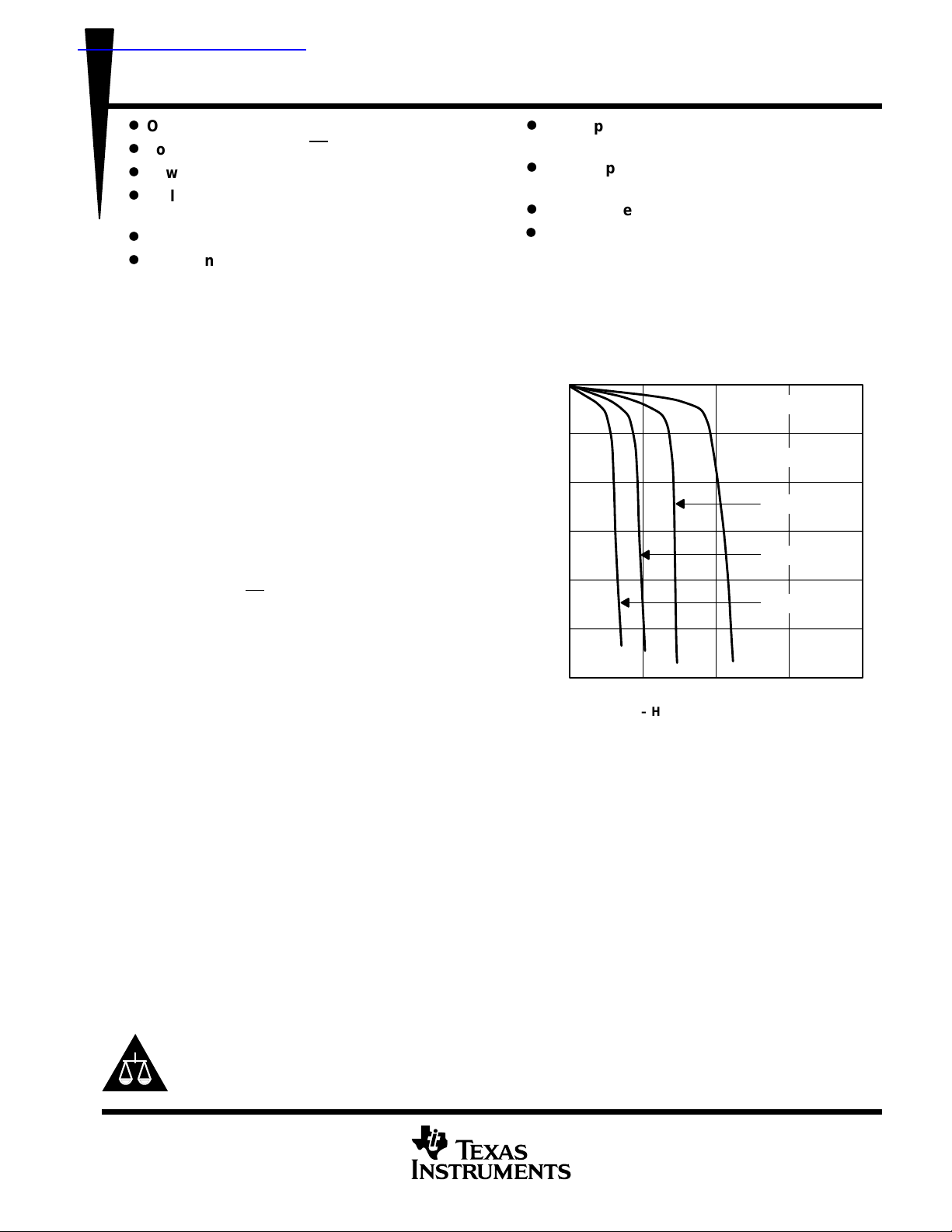
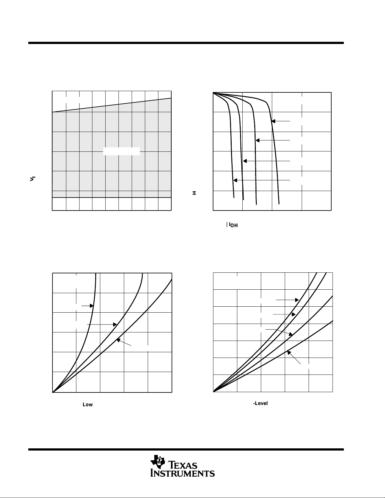
HIGH-LEVEL OUTPUT VOLTAGE
HIGH-LEVEL OUTPUT CURRENT
3
2.5
2
1.5
1
– High-Level Output Voltage – V
0.5
OH
V
0
0 200 400
| IOH | – High-Level Output Current – µA
= 25°C
A
vs
Figure 1
VDD = 3 V
TA = –40°C
TA = 25°C
TA = 85°C
TA = 125°C
600 800
The TL V2252/4 also make great upgrades to the TLV2322/4 in standard designs. They offer increased output
dynamic range, lower noise voltage, and lower input offset voltage. This enhanced feature set allows them to
be used in a wider range of applications. For applications that require higher output drive and wider input voltage
range, see the TLV2432 and TLV2442 devices. If your design requires single amplifiers, please see the
TL V221 1/21/31 family . These devices are single rail-to-rail operational amplifiers in the SOT -23 package. Their
small size and low power consumption, make them ideal for high density, battery-powered equipment.
Please be aware that an important notice concerning availability, standard warranty, and use in critical applications of
Texas Instruments semiconductor products and disclaimers thereto appears at the end of this data sheet.
Advanced LinCMOS is a trademark of Texas Instruments.
PRODUCTION DATA information is current as of publication date.
Products conform to specifications per the terms of Texas Instruments
standard warranty. Production processing does not necessarily include
testing of all parameters.
POST OFFICE BOX 655303 • DALLAS, TEXAS 75265
Copyright 2001, Texas Instruments Incorporated
On products compliant to MIL-PRF-38535, all parameters are tested
unless otherwise noted. On all other products, production
processing does not necessarily include testing of all parameters.
1
Page 2
TLV225x, TLV225xA
40°C to 125°C
µ
40°C to 125°C
µ
40°C to 125°C
µ
40°C to 125°C
µ
Advanced LinCMOS RAIL-TO-RAIL
VERY LOW-POWER OPERATIONAL AMPLIFIERS
SLOS185C – FEBRUARY 1997 – REVISED – MARCH 2001
TLV2252 AVAILABLE OPTIONS
PACKAGED DEVICES
T
A
–
–
–55°C to 125°C
†
The D packages are available taped and reeled. Add R suffix to device type (e.g., TL V2252CDR).
‡
The PW package is available only left-end taped and reeled.
§
Chips are tested at 25°C.
T
A
°
–
–
–55°C to 125°C
†
The D packages are available taped and reeled. Add R suffix to device type (e.g., TL V2254CDR).
‡
The PW package is available only left-end taped and reeled.
§
Chips are tested at 25°C.
°
VIOmax
AT 25°C
850 µV TLV2252AID — — TLV2252AIP TLV2252AIPWLE —
1500 µV
850 µV TLV2252AQD — — — — —
1500 µV
850 µV
1500 µV
VIOmax
AT 25°C
850 µV TLV2254AID — — TLV2254AIN TLV2254AIPWLE —
1500 µV
850 µV TLV2254AQD — — — — —
1500 µV
850 µV
1500 µV
SMALL
(D)
—
—
SMALL
(D)
—
—
†
†
OUTLINE
TLV2252ID — — TLV2252IP — —
TLV2252QD — — — — —
OUTLINE
TLV2254ID — — TLV2254IN — —
TLV2254QD — — — — —
CHIP
CARRIER
(FK)
TLV2252AMFK
TLV2252MFK
TLV2254 AVAILABLE OPTIONS
CHIP
CARRIER
(FK)
TLV2254AMFK
TLV2254MFK
CERAMIC
DIP
(JG)
TLV2252AMJG
TLV2252MJG
PACKAGED DEVICES
CERAMIC
DIP
(J)
TLV2254AMJ
TLV2254MJ
PLASTIC
PLASTIC
DIP
(P)
—
—
DIP
(N)
—
—
TSSOP
(PW)
—
—
TSSOP
(PW)
—
—
‡
‡
CERAMIC
FLATPACK
(U)
TLV2252AMU
TLV2252MU
CERAMIC
FLATPACK
(W)
TLV2254AMW
TLV2254MW
2
POST OFFICE BOX 655303 • DALLAS, TEXAS 75265
Page 3
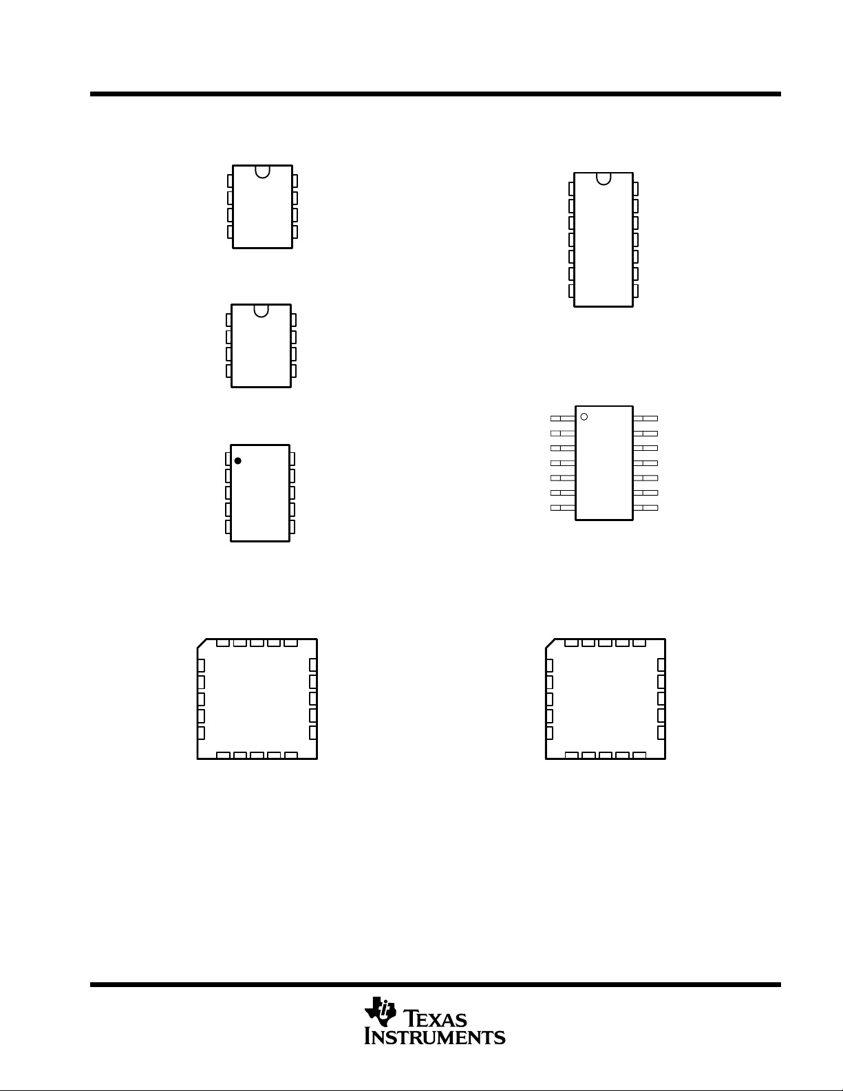
TLV2252I, TLV2252AI
E
TLV2252Q, TLV2252AQ
D, P, OR PW PACKAGE
(TOP VIEW)
TLV225x, TLV225xA
Advanced LinCMOS RAIL-TO-RAIL
VERY LOW-POWER OPERATIONAL AMPLIFIERS
SLOS185C – FEBRUARY 1997 – REVISED – MARCH 2001
TLV2254I, TLV2254AI, TLV2254Q, TL V2254AQ...D OR N PACKAG
TLV2254M, TLV2254AM ...J OR W PACKAGE
(TOP VIEW)
10
8
7
6
5
8
7
6
5
9
8
7
6
V
DD+
2OUT
2IN–
2IN+
V
DD+
2OUT
2IN–
2IN+
NC
V
CC
2OUT
2IN –
2IN +
+
1OUT
1IN–
1IN+
V
/GND
DD–
TLV2252M, TLV2252AM . . . JG PACKAGE
1OUT
1IN–
1IN+
V
/GND
DD–
TLV2252M, TLV2252AM ...U PACKAGE
1OUT
1IN –
1IN +
V
/GND
CC–
TLV2252M, TLV2252AM . . . FK PACKAGE
NC
1
2
3
4
(TOP VIEW)
1
2
3
4
(TOP VIEW)
1
2
3
4
5
(TOP VIEW)
1
14
13
12
10
14
4OUT
4IN–
4IN+
11
V
/GND
DD–
3IN+
9
3IN–
8
3OUT
4OUT
4IN –
4IN +
/GND
V
DD –
3IN +
3IN –
8
3OUT
1OUT
DD+
2
3
4
5
6
7
(TOP VIEW)
1
1IN–
1IN+
V
2IN+
2IN–
2OUT
TLV2254I, TLV2254AI . . . PW PACKAGE
1OUT
1IN –
1IN +
V
DD+
2IN +
2IN –
2OUT
TLV2254M, TLV2254AM . . . FK PACKAGE
7
(TOP VIEW)
NC
1IN–
NC
1IN+
NC
NC
1OUT
NC
3 2 1 20 19
4
5
6
7
8
910111213
NC
NC
/GND
DD–
V
DD+
V
2IN+
NC
18
17
16
15
14
NC
NC
2OUT
NC
2IN–
NC
1IN+
V
DD+
2IN+
NC
NC
1OUT
NC
4OUT
1IN –
3212019
4
5
6
7
8
910111213
NC
2IN –
2OUT
3OUT
4IN –
18
17
16
15
14
3IN –
4IN+
NC
V
DD–
NC
3IN+
/GND
POST OFFICE BOX 655303 • DALLAS, TEXAS 75265
3
Page 4
T
emplate Release Date: 7–11–
94
TLV225x, TLV2252xA
Advanced LinCMOSRAIL-TO-RAIL
VERY LOW-POWER OPERATIONAL AMPLIFIERS
SLOS185C – FEBRUARY 1997 – REVISED MARCH 2001
OUT
Q17Q15Q13
C1
DD+
V
R5
R6
D1
†
DD–/GND
V
ACTUAL DEVICE COMPONENT COUNT
COMPONENT TLV2252 TLV2254
Transistors 38 76
Resistors 30 56
Includes both amplifiers and all ESD, bias, and trim circuitry
Diodes 9 18
Capacitors 3 6
†
Q3 Q6 Q9 Q12 Q14 Q16
equivalent schematic (each amplifier)
4
Q4Q1
Q2 Q5 Q7 Q8 Q10 Q11
R3 R4 R1 R2
IN+
IN–
POST OFFICE BOX 655303 DALLAS, TEXAS 75265
•
Page 5
TLV225x, TLV225xA
PACKAGE
A
UNIT
Advanced LinCMOS RAIL-TO-RAIL
VERY LOW-POWER OPERATIONAL AMPLIFIERS
SLOS185C – FEBRUARY 1997 – REVISED – MARCH 2001
absolute maximum ratings over operating free-air temperature range (unless otherwise noted)
Supply voltage, V
Differential input voltage, V
Input voltage range, V
Input current, I
Output current, I
Total current into V
Total current out of V
Duration of short-circuit current (at or below) 25°C (see Note 3) unlimited. . . . . . . . . . . . . . . . . . . . . . . . . . . . . .
Continuous total power dissipation See Dissipation Rating Table. . . . . . . . . . . . . . . . . . . . . . . . . . . . . . . . . . . . .
Operating free-air temperature range, T
Storage temperature range, T
Lead temperature 1,6 mm (1/16 inch) from case for 10 seconds: D, N, P, and PW packages 260°C. . . . . . .
†
Stresses beyond those listed under “absolute maximum ratings” may cause permanent damage to the device. These are stress ratings only, and
functional operation of the device at these or any other conditions beyond those indicated under “recommended operating conditions” is not
implied. Exposure to absolute-maximum-rated conditions for extended periods may affect device reliability.
NOTES: 1. All voltage values, except differential voltages, are with respect to V
2. Differential voltages are at the noninverting input with respect to the inverting input. Excessive current flows when input is brought
below V
3. The output may be shorted to either supply. Temperature and/or supply voltages must be limited to ensure that the maximum
DD–
dissipation rating is not exceeded.
(see Note 1) 16 V. . . . . . . . . . . . . . . . . . . . . . . . . . . . . . . . . . . . . . . . . . . . . . . . . . . . . . . . . . . .
DD
I
(each input) ±5 mA. . . . . . . . . . . . . . . . . . . . . . . . . . . . . . . . . . . . . . . . . . . . . . . . . . . . . . . . . . . . . . .
I
±50 mA. . . . . . . . . . . . . . . . . . . . . . . . . . . . . . . . . . . . . . . . . . . . . . . . . . . . . . . . . . . . . . . . . . . . . . .
O
DD+
DD–
(see Note 2) ±V
ID
(any input, see Note 1) V
. . . . . . . . . . . . . . . . . . . . . . . . . . . . . . . . . . . . . . . . . . . . . . . . . . .
. . . . . . . . . . . . . . . . . . . . . . . . . . . . . . . . . .
–0.3 V to V
DD–
±50 mA. . . . . . . . . . . . . . . . . . . . . . . . . . . . . . . . . . . . . . . . . . . . . . . . . . . . . . . . . . . . . . . . . .
±50 mA. . . . . . . . . . . . . . . . . . . . . . . . . . . . . . . . . . . . . . . . . . . . . . . . . . . . . . . . . . . . . . . .
: I Suffix –40°C to 125°C. . . . . . . . . . . . . . . . . . . . . . . . . . . . . . . . . . .
A
Q Suffix –40°C to 125°C. . . . . . . . . . . . . . . . . . . . . . . . . . . . . . . . . .
M Suffix –55°C to 125°C. . . . . . . . . . . . . . . . . . . . . . . . . . . . . . . . . .
–65°C to 150°C. . . . . . . . . . . . . . . . . . . . . . . . . . . . . . . . . . . . . . . . . . . . . . . . . . .
stg
J, JG, U, and W packages 300°C. . . . . . .
.
DD –
– 0.3 V.
DD+
†
DD
DISSIPATION RATING TABLE
T
≤ 25°C DERATING FACTOR T
POWER RATING ABOVE TA = 25°CAPOWER RATINGAPOWER RATING
D–8 725 mW 5.8 mW/°C 377 mW 145 mW
D–14 950 mW 7.6 mW/°C 494 mW 190 mW
FK 1375 mW 11.0 mW/°C 715 mW 275 mW
J 1375 mW 11.0 mW/°C 715 mW 275 mW
JG 1050 mW 8.4 mW/°C 546 mW 210 mW
N 1150 mW 9.2 mW/°C 598 mW 230 mW
P 1000 mW 8.0 mW/°C 520 mW 200 mW
PW–8 525 mW 4.2 mW/°C 273 mW 105 mW
PW–14 700 mW 5.6 mW/°C 364 mW 140 mW
U 700 mW 5.5 mW/°C 370 mW 150 mW
W 700 mW 5.5 mW/°C 370 mW 150 mW
recommended operating conditions
TLV225xI TLV225xQ TLV225xM
MIN MAX MIN MAX MIN MAX
Supply voltage, VDD(see Note 1)
Input voltage range, V
Common-mode input voltage, V
Operating free-air temperature, T
NOTE 1: All voltage values, except differential voltages, are with respect to V
I
IC
A
2.7 16 2.7 16 2.7 16 V
V
DD–VDD+
V
DD–VDD+
–40 125 –40 125 –55 125 °C
–1.3 V
–1.3 V
DD –
= 85°C T
DD–VDD+
DD–VDD+
.
–1.3 V
–1.3 V
= 125°C
DD–VDD+
DD–VDD+
–1.3 V
–1.3 V
POST OFFICE BOX 655303 • DALLAS, TEXAS 75265
5
Page 6
TLV225x, TLV225xA
PARAMETER
TEST CONDITIONS
T
†
UNIT
VIOIn ut offset voltage
µV
0.5
0.5µV/°C
V
1.5 V
V
0
V
O
R
S
Ω
V
ICR
R
S
|V
IO
mV
V
V
OH
g
I
OH
µA
V
V
IC
I
OL
µA
V
OL
V
IC
I
OL
500 µA
mV
V
IC
I
OL
m
A
L
diff
l
V
1.5 V
R
100 kΩ
‡
voltage am lification
V
O
V
CMRR
IC
dB
Advanced LinCMOS RAIL-TO-RAIL
VERY LOW-POWER OPERATIONAL AMPLIFIERS
SLOS185C – FEBRUARY 1997 – REVISED – MARCH 2001
TLV2252I electrical characteristics at specified free-air temperature, VDD = 3 V (unless otherwise
noted)
A
p
α
I
I
A
r
r
c
z
†
‡
NOTE 4: Typical values are based on the input offset voltage shift observed through 500 hours of operating life test at TA = 150°C extrapolated
Temperature coefficient
VIO
of input offset voltage
Input offset voltage
long-term drift (see
Note 4)
Input offset current
IO
Input bias current
IB
Common-mode input
voltage range
High-level output
voltage
Low-level output
voltage
VD
i(d)
i(c)
i(c)
o
Full range is – 40°C to 125°C.
Referenced to 1.5 V
arge-signal
Differential input
resistance
Common-mode input
resistance
Common-mode input
capacitance
Closed-loop output
impedance
Common-mode VIC = 0 to 1.7 V,
rejection ratio
to TA = 25°C using the Arrhenius equation and assuming an activation energy of 0.96 eV .
erentia
p
= ±
DD±
= 0,
= 50 Ω,
IOH = –20 µA 25°C 2.98 2.98
= –75
IOH = –150 µA 25°C 2.8 2.8
= 1.5 V,
= 1.5 V,
= 1.5 V,
=
IC
= 1 V to 2
f = 10 kHz, P package 25°C 8 8 pF
f = 25 kHz, AV = 10 25°C 220 220
VO = 1.5 V, RS = 50 Ω
,
,
,
=
IC
=
= 50
| ≤5
= 50
=
= 1
=
L
RL = 1 MΩ
25°C 200 1500 200 850
Full range 1750 1000
25°C
to 85°C
25°C 0.003 0.003 µV/mo
25°C 0.5 60 0.5 60
–40°C
to 85°C
Full range 1000 1000
25°C 1 60 1 60
–40°C
to 85°C
Full range 1000 1000
25°C
Full range
25°C 2.9 2.9
Full range 2.8 2.8
25°C 10 10
Full range 80 80
25°C 100 100
Full range 150 150
25°C 200 200
Full range 300 300
25°C 100 250 100 250
Full range 10 10 V/mV
‡
25°C 800 800
25°C 10
25°C 10
25°C 65 75 65 77
Full range 60 60
TLV2252I TLV2252AI
MIN TYP MAX MIN TYP MAX
150 150
150 150
0 –0.3 0 –0.3
to to to to
2 2.2 2 2.2
0 0
to to
1.7 1.7
12
12
10
10
12
12
pA
pA
Ω
Ω
Ω
6
POST OFFICE BOX 655303 • DALLAS, TEXAS 75265
Page 7
TLV225x, TLV225xA
PARAMETER
TEST CONDITIONS
T
†
UNIT
k
SVR
rejection ratio
DD
dB
IDDSu ly current
V
O
No load
µA
PARAMETER
TEST CONDITIONS
T
†
UNIT
0.07
0.1
0.07
0.1
O
C
‡
0.05
0.05
V
q
V/√H
V
V
,
‡
,
Gain-bandwidth product
f 1 kHz,
R
L
kΩ ,
25°C
0.187
0.187
MHz
B
g
O(PP)
,
V
,
25°C6060
kHz
‡
L,L
Advanced LinCMOS RAIL-TO-RAIL
VERY LOW-POWER OPERATIONAL AMPLIFIERS
SLOS185C – FEBRUARY 1997 – REVISED – MARCH 2001
TLV2252I electrical characteristics at specified free-air temperature, VDD = 3 V (unless otherwise
noted) (continued)
A
Supply voltage
(∆VDD /∆VIO)
pp
†
Full range is – 40°C to 125°C.
VDD = 2.7 V to 8 V,
VIC = VDD/2, No load
= 1.5 V,
25°C 80 95 80 100
Full range 80 80
25°C 68 125 68 125
Full range 150 150
TLV2252I operating characteristics at specified free-air temperature, VDD = 3 V
A
TLV2252I TLV2252AI
MIN TYP MAX MIN TYP MAX
TLV2252I TLV2252AI
MIN TYP MAX MIN TYP MAX
SR Slew rate at unity gain
n
N(PP)
I
n
OM
φ
m
†
Full range is –40°C to 125°C.
‡
Referenced to 1.5 V
Equivalent input noise
voltage
Peak-to-peak
equivalent input noise
voltage
Equivalent input noise
current
Maximum output-swingV
bandwidth
Phase margin at unity
gain
Gain margin
p
p
VO = 1.1 V to 1.9 V,
RL = 100 kه,
= 100 pF
L
f = 10 Hz 25°C 35 35
f = 1 kHz
f = 0.1 Hz to 1 Hz 25°C 0.6 0.6
f = 0.1 Hz to 10 Hz
f = 1 kHz
CL = 100 pF
= 1 V, A
RL = 50 kه,
R
= 50 kه, C
‡
R
= 50 kΩ
50
= 1,
CL = 100 pF
= 100 pF
25°C
Full
range
25°C 19 19
25°C 1.1 1.1
25°C 0.6 0.6
‡
25°C 63° 63°
25°C 15 15 dB
V/µs
n
µ
fA/√Hz
z
POST OFFICE BOX 655303 • DALLAS, TEXAS 75265
7
Page 8
TLV225x, TLV225xA
PARAMETER
TEST CONDITIONS
T
†
UNIT
VIOInput offset voltage
V
0.5
0.5µV/°C
V
V
V
IC
V
|V
| ≤5 mV
R
50 Ω
V
VOHHigh-level output voltage
I
75 µA
V
V
2.5 V
I
50 µA
VOLLow-level output voltage
V
2.5 V
I
500 µA
V
V
2.5 V
I
1 m
A
R
100 kΩ
‡
voltage am lification
V
O
V
V
V
CMRR
j
IC
O
dB
Advanced LinCMOS RAIL-TO-RAIL
VERY LOW-POWER OPERATIONAL AMPLIFIERS
SLOS185C – FEBRUARY 1997 – REVISED – MARCH 2001
TLV2252I electrical characteristics at specified free-air temperature, VDD = 5 V (unless otherwise
noted)
A
p
α
I
I
A
r
r
c
z
†
‡
NOTE 4: Typical values are based on the input offset voltage shift observed through 500 hours of operating life test at TA = 150°C extrapolated
Temperature coefficient
VIO
of input offset voltage
Input offset voltage long-
term drift (see Note 4)
Input offset current
IO
Input bias current
IB
Common-mode input
ICR
voltage range
p
p
Large-signal differentialpVIC = 2.5 V,
VD
Differential input
i(d)
resistance
Common-mode input
i(c)
resistance
Common-mode input
i(c)
capacitance
Closed-loop output
o
impedance
Common-mode rejection VIC = 0 to 2.7 V,
ratio
Full range is – 40°C to 125°C.
Referenced to 2.5 V
to TA = 25°C using the Arrhenius equation and assuming an activation energy of 0.96 eV .
,
,
,
,
,
= 0,
IC
RS = 50 Ω
=
S
=
OL
=
OL
=
OL
=
L
RL = 1 MΩ
= 2.5
O
= ±2.5
DD±
VO = 0,
IO
IOH = –20 µA 25°C 4.98 4.98
= –
OH
IOH = –150 µA 25°C 4.8 4.88 4.8 4.88
=
IC
=
IC
=
IC
= 1 V to 4
f = 10 kHz, P package 25°C 8 8 pF
f = 25 kHz, AV = 10 25°C 200 200
RS = 50 Ω
25°C 200 1500 200 850
Full range 1750 1000
25°C
to 85°C
25°C 0.003 0.003 µV/mo
25°C
–40°C
to 85°C
Full range 1000 1000
25°C 1 60 1 60
–40°C
to 85°C
Full range 1000 1000
25°C
Full range
25°C 4.9 4.94 4.9 4.94
Full range 4.8 4.8
25°C 0.01 0.01
Full range 0.06 0.06
25°C 0.09 0.15 0.09 0.15
Full range 0.15 0.15
25°C 0.2 0.3 0.2 0.3
Full range 0.3 0.3
25°C 100 350 100 350
Full range 10 10
‡
25°C 1700 1700
25°C 10
25°C 10
25°C 70 83 70 83
,
Full range 70 70
TLV2252I TLV2252AI
MIN TYP MAX MIN TYP MAX
0.5 60 0.5 60
150 150
150 150
0
3.5
–0.3
to
to
4
4.2
0
to
12
12
3.5
0
–0.3
to
to
4
4.2
0
to
12
10
12
10
µ
°
pA
pA
V/mV
Ω
Ω
Ω
8
POST OFFICE BOX 655303 • DALLAS, TEXAS 75265
Page 9
TLV225x, TLV225xA
PARAMETER
TEST CONDITIONS
T
†
UNIT
k
ygj
DD
dB
IDDSu ly current
V
O
No load
µA
PARAMETER
TEST CONDITIONS
T
†
UNIT
25°C
0.07
0.12
0.07
0.12
V
1.5 V to 3.5 V
‡
R
100 kΩ
‡
C
L
100 F
‡
0.05
0.05
V
q
V/√H
V
equivalent input
V
THD
N
f
kHz
25°C
,
L
,
25°C
0.2
0.2
MHz
B
g
O(PP)
,
V
,
25°C3030
kHz
‡
L,L
Advanced LinCMOS RAIL-TO-RAIL
VERY LOW-POWER OPERATIONAL AMPLIFIERS
SLOS185C – FEBRUARY 1997 – REVISED – MARCH 2001
TLV2252I electrical characteristics at specified free-air temperature, VDD = 5 V (unless otherwise
noted) (continued)
A
Supply voltage rejection VDD = 4.4 V to 8 V,
SVR
ratio (∆VDD/∆VIO)
pp
†
Full range is – 40°C to 125°C.
VIC = VDD/2, No load
= 2.5 V,
25°C 80 95 80 95
Full range 80 80
25°C 70 125 70 125
Full range 150 150
TLV2252I operating characteristics at specified free-air temperature, VDD = 5 V
A
TLV2252I TLV2252AI
MIN TYP MAX MIN TYP MAX
TLV2252I TLV2252AI
MIN TYP MAX MIN TYP MAX
SR Slew rate at unity gain
n
N(PP)
I
n
OM
φ
m
†
Full range is – 40°C to 125°C.
‡
Referenced to 2.5 V
Equivalent input noise
voltage
Peak-to-peak
noise voltage
Equivalent input noise
current
Total harmonic
+
distortion plus noise
Gain-bandwidth
product
Maximum output-swingV
bandwidth
Phase margin at unity
gain
Gain margin
p
=
O
p
=
f = 10 Hz 25°C 36 36
f = 1 kHz
f = 0.1 Hz to 1 Hz 25°C 0.7 0.7
f = 0.1 Hz to 10 Hz
VO = 0.5 V to 2.5 V,
= 20
RL = 50 kΩ
f = 50 kHz, RL = 50 kه,
CL = 100 pF
= 2 V, A
RL = 50 kΩ
R
= 50 kه, C
,
=
L
,
‡
‡
‡,
AV = 1
AV = 10
= 1,
CL = 100 pF
= 100 pF
,
Full
range
25°C 19 19
25°C 1.1 1.1
25°C 0.6 0.6
0.2% 0.2%
1% 1%
°
‡
25°C 63° 63°
25°C 15 15 dB
V/µs
n
µ
fA/√Hz
z
POST OFFICE BOX 655303 • DALLAS, TEXAS 75265
9
Page 10
TLV225x, TLV225xA
PARAMETER
TEST CONDITIONS
T
†
UNIT
VIOInput offset voltage
V
coefficient of input
0.5
0.5µV/°C
,
V
DD±
±1.5 V,
V
IC
0,
25°C
V
S
|V
| ≤5 mV
V
Full range
V
g
I
75 µA
V
V
1.5 V
I
50 µA
V
V
1.5 V
I
500 µA
mV
V
1.5 V
I
1 m
A
gg
V
1.5 V
R
100 kΩ
‡
V
O
V
CMRR
IC
O
dB
Advanced LinCMOS RAIL-TO-RAIL
VERY LOW-POWER OPERATIONAL AMPLIFIERS
SLOS185C – FEBRUARY 1997 – REVISED – MARCH 2001
TLV2254I electrical characteristics at specified free-air temperature, VDD = 3 V (unless otherwise
noted)
A
p
Temperature
α
VIO
offset voltage
Input offset voltage
long-term drift
(see Note 4)
I
I
A
r
r
c
z
†
‡
NOTE 4: Typical values are based on the input offset voltage shift observed through 500 hours of operating life test at TA = 150°C extrapolated
Input offset current
IO
Input bias current
IB
Common-mode input RS = 50 Ω,
ICR
voltage range
High-level output
OH
voltage
Low-level output
OL
voltage
Large-signal
differential voltage
VD
amplification
Differential input
i(d)
resistance
Common-mode input
i(c)
resistance
Common-mode input
i(c)
capacitance
Closed-loop output
o
impedance
Common-mode VIC = 0 to 1.7 V, VO = 1.5 V,
rejection ratio
Full range is – 40°C to 125°C.
Referenced to 1.5 V
to TA = 25°C using the Arrhenius equation and assuming an activation energy of 0.96 eV .
p
V
= ±1.5 V,V
VO = 0,
IOH = –20 µA 25°C 2.98 2.98
= –
OH
IOH = –150 µA 25°C 2.8 2.8
,
=
IC
,
=
IC
,
=
IC
,
=
IC
= 1 V to 2
f = 10 kHz, N package 25°C 8 8 pF
f = 25 kHz, AV = 10 25°C 220 220 Ω
RS = 50 Ω
= 0
RS = 50 Ω
IO
=
OL
=
OL
=
OL
=
L
RL = 1 MΩ
25°C 200 1500 200 850
Full range 1750 1000
25°C
to 85°C
25°C 0.003 0.003 µV/mo
25°C 0.5 60 0.5 60
–40°C
to 85°C
Full range 1000 1000
25°C 1 60 1 60
–40°C
to 85°C
Full range 1000 1000
25°C 2.9 2.9
Full range 2.8 2.8
25°C 10 10
Full range 80 80
25°C 100 100
Full range 150 150
25°C 200 200
Full range 300 300
25°C 100 225 100 225
Full range 10 10 V/mV
‡
25°C 800 800
25°C 10
25°C 10
25°C 65 75 65 77
Full range 60 60
TLV2254I TLV2254AI
MIN TYP MAX MIN TYP MAX
150 150
150 150
0 –0.3 0 –0.3
to 2 to 2.2 to 2 to 2.2
0 0
to 1.7 to 1.7
12
12
10
10
12
12
µ
pA
pA
Ω
Ω
10
POST OFFICE BOX 655303 • DALLAS, TEXAS 75265
Page 11
TLV225x, TLV225xA
PARAMETER
TEST CONDITIONS
T
†
UNIT
k
rejection ratio
DD
dB
I
DD
y
V
O
No load
µA
PARAMETER
TEST CONDITIONS
T
†
UNIT
V
O
0.07
0.1
0.07
0.1
SR
Slew rate at unity gain
R
100 kΩ
‡
V/µs
C
F
‡
Full range
0.05
0.05
VnEquivalent input noise voltage
V/√H
V
q
V
Gain-bandwidth product
R
50 kΩ
‡
25°C
0.187
0.187
MHz
g
B
g
V
,
25°C6060
kHz
L
,
Advanced LinCMOS RAIL-TO-RAIL
VERY LOW-POWER OPERATIONAL AMPLIFIERS
SLOS185C – FEBRUARY 1997 – REVISED – MARCH 2001
TLV2254I electrical characteristics at specified free-air temperature, VDD = 3 V (unless otherwise
noted) (continued)
A
Supply voltage
SVR
(∆VDD/∆VIO)
Supply current
(four amplifiers)
†
Full range is – 40°C to 125°C.
VDD = 2.7 V to 8 V,
VIC = VDD/2, No load
= 1.5 V,
25°C 80 95 80 100
Full range 80 80
25°C 135 250 135 250
Full range 300 300
TLV2254I operating characteristics at specified free-air temperature, VDD = 3 V
A
N(PP)
I
n
OM
φ
m
†
Full range is – 40°C to 85°C.
‡
Referenced to 1.5 V
Peak-to-peak equivalent input
noise voltage
Equivalent input noise current 25°C 0.6 0.6
Maximum output-swin
bandwidth
Phase margin at unity gain
Gain margin
= 0.7 V to 1.7 V,
=
L
= 100 p
L
p
p
f = 10 Hz 25°C 35 35
f = 1 kHz 25°C 19 19
f = 0.1 Hz to 1 Hz 25°C 0.6 0.6
f = 0.1 Hz to 10 Hz
f = 1 kHz,
=
L
CL = 100 pF
V
O(PP)
= 1,
A
RL = 50 kه,
CL = 100 pF
R
= 50 kه,
CL = 100 pF
,
,
‡
= 1 V,
‡
‡
25°C
25°C 1.1 1.1
°
25°C 63° 63°
25°C 15 15 dB
TLV2254I TLV2254AI
MIN TYP MAX MIN TYP MAX
TLV2254I TLV2254AI
MIN TYP MAX MIN TYP MAX
n
µ
fA/√Hz
z
POST OFFICE BOX 655303 • DALLAS, TEXAS 75265
11
Page 12
TLV225x, TLV225xA
PARAMETER
TEST CONDITIONS
T
†
UNIT
VIOInput offset voltage
V
coefficient of input
0.5
0.5µV/°C
V
DD±
±2.5 V,
V
IC
25°C
V
|V
| ≤5 mV
R
50 Ω
V
Full range
V
g
I
75 µA
V
V
2.5 V
I
50 µA
V
V
2.5 V
I
500 µA
V
V
2.5 V
I
1 m
A
Large signal
V
2.5 V
R
100 kΩ
‡
VD
V
O
V
CMRR
IC
,
O
,
dB
Advanced LinCMOS RAIL-TO-RAIL
VERY LOW-POWER OPERATIONAL AMPLIFIERS
SLOS185C – FEBRUARY 1997 – REVISED – MARCH 2001
TLV2254I electrical characteristics at specified free-air temperature, VDD = 5 V (unless otherwise
noted)
A
p
Temperature
α
VIO
offset voltage
Input offset voltage
long-term drift
(see Note 4)
I
I
A
r
r
c
z
†
‡
NOTE 4: Typical values are based on the input offset voltage shift observed through 500 hours of operating life test at TA = 150°C extrapolated
Input offset current
IO
Input bias current
IB
Common-mode input
ICR
voltage range
High-level output
OH
voltage
Low-level output
OL
voltage
Large-signal
differential voltage
VD
amplification
Differential input
i(d)
resistance
Common-mode input
i(c)
resistance
Common-mode input
i(c)
capacitance
Closed-loop output
o
impedance
Common-mode V
rejection ratio
Full range is – 40°C to 125°C.
Referenced to 2.5 V
to TA = 25°C using the Arrhenius equation and assuming an activation energy of 0.96 eV .
p
V
= ±2.5 V,V
VO = 0,
IO
IOH = –20 µA 25°C 4.98 4.98
= –
OH
IOH = –150 µA 25°C 4.8 4.88 4.8 4.88
=
IC
=
IC
=
IC
=
IC
= 1 V to 4
f = 10 kHz, N package 25°C 8 8 pF
f = 25 kHz, AV = 10 25°C 200 200 Ω
= 0 to 2.7 V, V
RS = 50 Ω
,
,
,
,
,
= 0,
0,
RS = 50 Ω
=
S
=
OL
=
OL
=
OL
=
L
RL = 1 MΩ
= 2.5 V,
25°C 200 1500 200 850
Full range 1750 1000
25°C
to 85°C
25°C
25°C
–40°C
to 85°C
Full range 1000 1000
25°C 1 60 1 60
–40°C
to 85°C
Full range 1000 1000
25°C 4.9 4.94 4.9 4.94
Full range 4.8 4.8
25°C 0.01 0.01
Full range 0.06 0.06
25°C 0.09 0.15 0.09 0.15
Full range 0.15 0.15
25°C 0.2 0.3 0.2 0.3
Full range 0.3 0.3
25°C 100 350 100 350
Full range 10 10
‡
25°C 1700 1700
25°C 10
25°C 10
25°C 70 83 70 83
Full range 70 70
TLV2254I TLV2254AI
MIN TYP MAX MIN TYP MAX
0.003 0.003 µV/mo
0.5 60 0.5 60
150 150
150 150
0 –0.3 0 –0.3
to 4 to 4.2 to 4 to 4.2
0 0
to 3.5 to 3.5
12
12
10
10
12
12
µ
pA
pA
V/mV
Ω
Ω
12
POST OFFICE BOX 655303 • DALLAS, TEXAS 75265
Page 13
TLV225x, TLV225xA
PARAMETER
TEST CONDITIONS
T
†
UNIT
k
rejection ratio
DD
dB
I
y
V
2.5 V
No load
A
PARAMETER
TEST CONDITIONS
T
†
UNIT
Slew rate at unity
V
1.4 V to 2.6 V
R
100 kΩ
‡
V
q
V/√H
V
equivalent input
V
THD
N
distortion plus
f
kHz
25°C
,
L
,
25°C
0.2
0.2
MHz
B
O(PP)
,
V
,
25°C3030
kHz
‡
L,L
Advanced LinCMOS RAIL-TO-RAIL
VERY LOW-POWER OPERATIONAL AMPLIFIERS
SLOS185C – FEBRUARY 1997 – REVISED – MARCH 2001
TLV2254I electrical characteristics at specified free-air temperature, VDD = 5 V (unless otherwise
noted) (continued)
A
Supply voltage
SVR
(∆VDD/∆VIO)
Supply current
DD
(four amplifiers)
†
Full range is – 40°C to 125°C.
VDD = 4.4 V to 8 V,
VIC = VDD/2, No load
,
=
O
25°C 80 95 80 95
Full range 80 80
25°C 140 250 140 250
Full range 300 300
TLV2254I operating characteristics at specified free-air temperature, VDD = 5 V
A
25°C
,
Full
range
25°C 19 19
25°C 1.1 1.1
25°C 0.6 0.6
‡
°
25°C 63° 63°
25°C 15 15 dB
SR
n
N(PP)
I
n
OM
φ
m
†
Full range is – 40°C to 125°C.
‡
Referenced to 2.5 V
gain
Equivalent input
noise voltage
Peak-to-peak
noise voltage
Equivalent input
noise current
Total harmonic
+
noise
Gain-bandwidth
product
Maximum output- V
swing bandwidth
Phase margin at
unity gain
Gain margin
p
p
=
O
CL = 100 pF
f = 10 Hz 25°C 36 36
f = 1 kHz
f = 0.1 Hz to 1 Hz 25°C 0.7 0.7
f = 0.1 Hz to 10 Hz
VO = 0.5 V to 2.5 V,
= 20
RL = 50 kΩ
f = 50 kHz, R
CL = 100 pF
= 2 V, A
RL = 50 kه,
R
= 50 kه, C
,
=
‡
,
‡
‡
L
AV = 1
AV = 10
= 50 kه,
= 1,
CL = 100 pF
= 100 pF
TLV2254I TLV2254AI
MIN TYP MAX MIN TYP MAX
TLV2254I TLV2254AI
MIN TYP MAX MIN TYP MAX
0.07 0.12 0.07 0.12
0.05 0.05
0.2% 0.2%
1% 1%
µ
V/µs
n
µ
fA/√Hz
z
POST OFFICE BOX 655303 • DALLAS, TEXAS 75265
13
Page 14
TLV225x, TLV225xA
A
VIOIn ut offset voltage
µV
0.5
0.5µV/°C
V
V
V
IIOIn ut offset current
A
IIBIn ut bias current
A
V
ICR
R
S
|V
IO
mV
V
V
OH
g
I
OH
µA
V
Low-level output
V
IC
I
OL
500 µA
voltage
V
IC
I
OL
m
A
L
diff
l
V
1.5 V
R
100 kΩ
‡
voltage am lification
V
O
V
CMRR
j
IC
O
dB
k
SVR
ygj
DD
dB
IDDSupply current
V
1.5 V
No load
A
Advanced LinCMOS RAIL-TO-RAIL
VERY LOW-POWER OPERATIONAL AMPLIFIERS
SLOS185C – FEBRUARY 1997 – REVISED – MARCH 2001
TLV2252Q, and TLV2252M electrical characteristics at specified free-air temperature, VDD = 3 V
(unless otherwise noted)
TLV2252Q,
PARAMETER TEST CONDITIONS
p
α
V
A
r
r
c
z
†
‡
NOTE 4: Typical values are based on the input offset voltage shift observed through 500 hours of operating life test at TA = 150°C extrapolated
Temperature coefficient
VIO
of input offset voltage
Input offset voltage
long-term drift
(see Note 4)
p
p
Common-mode input
voltage range
High-level output
voltage
OL
VD
i(d)
i(c)
i(c)
o
Full range is –40°C to 125°C for Q level part, –55°C to 125°C for M level part.
Referenced to 1.5 V
arge-signal
Differential input
resistance
Common-mode input
resistance
Common-mode input
capacitance
Closed-loop output
impedance
Common-mode rejection VIC = 0 to 1.7 V, VO = 1.5 V,
ratio
Supply voltage rejection VDD = 2.7 V to 8 V,
ratio (∆VDD /∆VIO)
pp
to TA = 25°C using the Arrhenius equation and assuming an activation energy of 0.96 eV .
p
erentia
p
= ±1.5
DD±
VO = 0,
= 50 Ω,
IOH = –20 µA 25°C 2.98 2.98
= –75
IOH = –150 µA 25°C 2.8 2.8
VIC = 1.5 V, IOL = 50 µA 25°C 10 10
= 1.5 V,
= 1.5 V,
=
IC
= 1 V to 2
f = 10 kHz, P package 25°C 8 8 pF
f = 25 kHz, AV = 10 25°C 220 220
RS = 50 Ω
VIC = VDD/2, No load
=
O
,
,
,
IC
RS = 50 Ω
RL = 1 MΩ
L
= 0,
| ≤5
=
= 1
=
‡
†
T
25°C 200 1500 200 850
Full range 1750 1000
25°C
to 85°C
25°C
25°C 0.5 60 0.5 60
125°C 1000 1000
25°C 1 60 1 60
125°C 1000 1000
25°C
Full range
25°C 2.9 2.9
Full range 2.8 2.8
25°C 100 150 100 150
Full range 165 165 mV
25°C 200 300 200 300
Full range 300 300
25°C 100 250 100 250
Full range 10 10 V/mV
25°C 800 800
25°C 10
25°C 10
25°C 65 75 65 77
Full range 60 60
25°C 80 95 80 100
Full range 80 80
25°C 68 125 68 125
Full range 150 150
TLV2252M
MIN TYP MAX MIN TYP MAX
0.003 0.003 µV/mo
0 –0.3 0 –0.3
to to to to
2 2.2 2 2.2
0 0
to to
1.7 1.7
12
12
TLV2252AQ,
TLV2252AM
12
10
12
10
UNIT
p
p
Ω
Ω
Ω
µ
14
POST OFFICE BOX 655303 • DALLAS, TEXAS 75265
Page 15
TLV225x, TLV225xA
A
25°C
0.07
0.1
0.07
0.1
V
0.8 V to 1.4 V
R
100 kΩ
‡
C
L
100 F
‡
0.05
0.05
V
q
V/√H
V
t
V
‡
,
f 1 kHz,
R
L
kΩ ,
25°C
0.187
0.187
MHz
B
O(PP)
,
V
,
25°C6060
kHz
‡
L,L
Advanced LinCMOS RAIL-TO-RAIL
VERY LOW-POWER OPERATIONAL AMPLIFIERS
SLOS185C – FEBRUARY 1997 – REVISED – MARCH 2001
TLV2252Q, and TLV2252M operating characteristics at specified free-air temperature, VDD = 3 V
PARAMETER TEST CONDITIONS
TLV2252Q,
†
T
TLV2252M
MIN TYP MAX MIN TYP MAX
TLV2252AQ,
TLV2252AM
UNIT
=
SR Slew rate at unity gain
n
N(PP)
I
n
OM
φ
m
†
Full range is –40°C to 125°C for Q level part, –55°C to 125°C for M level part.
‡
Referenced to 1.5 V
Equivalent input noise
voltage
Peak-to-peak
equivalent inpu
noise voltage
Equivalent input noise
current
Gain-bandwidth
product
Maximum
p
output-swing
bandwidth
Phase margin at unity
gain
Gain margin
p
O
=
=
p
f = 10 Hz 25°C 35 35
f = 1 kHz
f = 0.1 Hz to 1 Hz 25°C 0.6 0.6
f = 0.1 Hz to 10 Hz
f = 1 kHz, R
CL = 100 pF
V
RL = 50 kه,
R
= 1 V, A
= 50 kه, C
,
=
‡
‡
L
= 50 kΩ
50
= 1,
CL = 100 pF
= 100 pF
,
‡
Full
range
25°C 19 19
25°C 1.1 1.1
25°C 0.6 0.6
°
25°C 63° 63°
25°C 15 15 dB
V/µs
n
fA/√Hz
z
µ
POST OFFICE BOX 655303 • DALLAS, TEXAS 75265
15
Page 16

TLV225x, TLV225xA
A
VIOInput offset voltage
V
0.5
0.5µV/°C
V
V
V
IIOInput offset current
pA
IIBInput bias current
pA
V
|V
| ≤5 mV
R
50 Ω
V
VOHHigh-level output voltage
I
75 µA
V
V
2.5 V
I
500 µA
V
2.5 V
I
1 m
A
R
100 kΩ
‡
voltage am lification
V
O
V
CMRR
j
IC
,
dB
k
ygj
DD
dB
Advanced LinCMOS RAIL-TO-RAIL
VERY LOW-POWER OPERATIONAL AMPLIFIERS
SLOS185C – FEBRUARY 1997 – REVISED – MARCH 2001
TLV2252Q, and TLV2252M electrical characteristics at specified free-air temperature, VDD = 5 V
(unless otherwise noted)
TLV2252Q,
PARAMETER TEST CONDITIONS
p
α
V
A
r
r
c
z
†
‡
NOTE 4: Typical values are based on the input offset voltage shift observed through 500 hours of operating life test at TA = 150°C extrapolated
Temperature coefficient
VIO
of input offset voltage
Input offset voltage long-
term drift (see Note 4)
p
p
Common-mode input
ICR
voltage range
p
Low-level output voltage
OL
Large-signal differentialpVIC = 2.5 V,
VD
Differential input
i(d)
resistance
Common-mode input
i(c)
resistance
Common-mode input
i(c)
capacitance
Closed-loop output
o
impedance
Common-mode rejection
ratio
Supply voltage rejection VDD = 4.4 V to 8 V,
SVR
ratio (∆VDD/∆VIO)
Full range is –40°C to 125°C for Q level part, –55°C to 125°C for M level part.
Referenced to 2.5 V
to TA = 25°C using the Arrhenius equation and assuming an activation energy of 0.96 eV .
= ±2.5
DD±
VO = 0,
IO
IOH = –20 µA 25°C 4.98 4.98
= –
OH
IOH = –150 µA 25°C 4.8 4.88 4.8 4.88
VIC = 2.5 V, IOL = 50 µA 25°C 0.01 0.01
=
IC
=
IC
= 1 V to 4
f = 10 kHz, P package 25°C 8 8 pF
f = 25 kHz, AV = 10 25°C 200 200
V
= 0 to 2.7 V,
VO = 2.5 V, RS = 50 Ω
VIC = VDD/2, No load
,
,
,
,
IC
RS = 50 Ω
S
OL
OL
L
RL = 1 MΩ
= 0,
=
=
=
=
‡
†
T
25°C 200 1500 200 850
Full range 1750 1000
25°C
to 85°C
25°C
25°C 0.5 60 0.5 60
125°C 1000 1000
25°C 1 60 1 60
125°C 1000 1000
25°C
Full range
25°C 4.9 4.94 4.9 4.94
Full range 4.8 4.8
25°C 0.09 0.15 0.09 0.15
Full range 0.15 0.15
25°C 0.2 0.3 0.2 0.3
Full range 0.3 0.3
25°C 100 350 100 350
Full range 10 10
25°C 1700 1700
25°C 10
25°C 10
25°C 70 83 70 83
Full range 70 70
25°C 80 95 80 95
Full range 80 80
TLV2252M
MIN TYP MAX MIN TYP MAX
0.003 0.003 µV/mo
0
–0.3
to
to
4
4.2
0
to
3.5
12
12
TLV2252AQ,
TLV2252AM
0
–0.3
to
4
4.2
0
to
3.5
12
10
12
10
UNIT
µ
p
p
to
V
V/mV
Ω
Ω
Ω
16
POST OFFICE BOX 655303 • DALLAS, TEXAS 75265
Page 17
TLV225x, TLV225xA
A
IDDSupply current
V
2.5 V
No load
A
A
0.07
0.12
0.07
0.12
C
F
‡
0.05
0.05
V
q
V/√H
V
equivalent input
V
THD
N
f
kHz
25°C
Gain-bandwidth product
,
L
,
25°C
0.2
0.2
MHz
B
g
O(PP)
,
V
,
25°C3030
kHz
‡
L,L
Advanced LinCMOS RAIL-TO-RAIL
VERY LOW-POWER OPERATIONAL AMPLIFIERS
SLOS185C – FEBRUARY 1997 – REVISED – MARCH 2001
TLV2252Q, and TLV2252M electrical characteristics at specified free-air temperature, VDD = 5 V
(unless otherwise noted) (continued)
TLV2252Q,
PARAMETER TEST CONDITIONS
pp
†
Full range is –40°C to 125°C for Q level part, –55°C to 125°C for M level part.
O
=
,
Full range 150 150
†
T
25°C 70 125 70 125
TLV2252M
MIN TYP MAX MIN TYP MAX
TLV2252Q, and TLV2252M operating characteristics at specified free-air temperature, VDD = 5 V
TLV2252Q,
PARAMETER TEST CONDITIONS
†
T
TLV2252M
MIN TYP MAX MIN TYP MAX
TLV2252AQ,
TLV2252AM
TLV2252AQ,
TLV2252AM
UNIT
µ
UNIT
VO = 1.25 V to 2.75 V,
SR Slew rate at unity gain
n
N(PP)
I
n
OM
φ
m
†
Full range is –40°C to 125°C for Q level part, –55°C to 125°C for M level part.
‡
Referenced to 2.5 V
Equivalent input noise
voltage
Peak-to-peak
noise voltage
Equivalent input noise
current
Total harmonic
+
distortion plus noise
Maximum output-swingV
bandwidth
Phase margin at unity
gain
Gain margin
p
p
RL = 100 kه,
= 100 p
L
f = 10 Hz 25°C 36 36
f = 1 kHz
f = 0.1 Hz to 1 Hz 25°C 0.7 0.7
f = 0.1 Hz to 10 Hz
VO = 0.5 V to 2.5 V,
= 20
RL = 50 kΩ
f = 50 kHz, RL = 50 kه,
CL = 100 pF
RL = 50 kه,
R
,
‡
‡
= 2 V, A
= 50 kه, C
AV = 1
AV = 10
= 1,
CL = 100 pF
= 100 pF
‡
25°C
Full
range
25°C 19 19
25°C 1.1 1.1
25°C 0.6 0.6
0.2% 0.2%
1% 1%
°
25°C 63° 63°
25°C 15 15 dB
V/µs
n
µ
fA/√Hz
z
POST OFFICE BOX 655303 • DALLAS, TEXAS 75265
17
Page 18
TLV225x, TLV225xA
A
VIOInput offset voltage
V
0.5
0.5µV/°C
IIOInput offset current
pA
IIBInput bias current
pA
V
R
50 Ω
|V
| ≤5 mV
V
g
V
g
I
75 µA
V
L
t
V
1.5 V
I
500 µA
voltage
V
1.5 V
I
1 m
A
L
diff
l
V
1.5 V
R
100 kΩ
‡
VD
voltage am lification
V
O
V
CMRR
IC
O
dB
k
SVR
rejection ratio
DD
dB
Advanced LinCMOS RAIL-TO-RAIL
VERY LOW-POWER OPERATIONAL AMPLIFIERS
SLOS185C – FEBRUARY 1997 – REVISED – MARCH 2001
TLV2254Q, and TLV2254M electrical characteristics at specified free-air temperature, VDD = 3 V
(unless otherwise noted)
TLV2254Q,
PARAMETER TEST CONDITIONS
p
α
V
A
r
r
c
z
†
‡
NOTE 4: Typical values are based on the input offset voltage shift observed through 500 hours of operating life test at TA = 150°C extrapolated
Temperature coefficient 25°C
VIO
of input offset voltage to 125°C
Input offset voltage
longterm drift (see Note 4)
p
p
Common-mode input
ICR
voltage range
High-level output
OH
voltage
OL
VD
i(d)
i(c)
i(c)
o
Full range is –40°C to 125°C for Q level part, –55°C to 125°C for M level part.
Referenced to 1.5 V
ow-level outpu
arge-signal
Differential input
resistance
Common-mode input
resistance
Common-mode input
capacitance
Closed-loop output
impedance
Common-mode VIC = 0 to 1.7 V, VO = 1.5 V,
rejection ratio
Supply voltage
(∆VDD/∆VIO)
to TA = 25°C using the Arrhenius equation and assuming an activation energy of 0.96 eV .
erentia
p
V
= ±1.5 V ,
DD±
VO = 0,
,
=
S
IOH = –20 µA 25°C 2.98 2.98
= –
OH
IOH = –150 µA 25°C 2.8 2.8
VIC = 1.5 V, IOL = 50 µA 25°C 10 10
=
IC
=
IC
=
IC
= 1 V to 2
f = 10 kHz, N package 25°C 8 8 pF
f = 25 kHz, AV = 10 25°C 220 220 Ω
RS = 50 Ω
VDD = 2.7 V to 8 V,
VIC = VDD/2, No load
,
,
,
VIC = 0,
RS = 50 Ω
IO
=
OL
=
OL
=
L
RL = 1 MΩ
‡
†
T
25°C 200 1500 200 850
Full range 1750 1000
25°C
25°C 0.5 60 0.5 60
125°C 1000 1000
25°C 1 60 1 60
125°C 1000 1000
25°C
Full range
25°C 2.9 2.9
Full range 2.8 2.8
25°C 100 150 100 150
Full range 165 165 mV
25°C 200 300 200 300
Full range 300 300
25°C 100 225 100 225
Full range 10 10
25°C 800 800
25°C 10
25°C 10
25°C 65 75 65 77
Full range 60 60
25°C 80 95 80 100
Full range 80 80
TLV2254M
MIN TYP MAX MIN TYP MAX
0.003 0.003 µV/mo
0 –0.3 0 –0.3
to to to to
2 2.2 2 2.2
0 0
to to
1.7 1.7
12
12
TLV2254AQ,
TLV2254AM
12
10
12
10
UNIT
µ
p
p
V/mV
Ω
Ω
18
POST OFFICE BOX 655303 • DALLAS, TEXAS 75265
Page 19

TLV225x, TLV225xA
A
I
DD
y
V
O
No load
µA
A
SR
Slew rate at unity gain
R
100 kΩ
‡
V/µs
C
F
‡
Full range
0.05
0.05
VnEquivalent input noise voltage
V/√H
V
q
V
Gain-bandwidth product
R
50 kΩ
‡
25°C
0.187
0.187
MHz
g
B
g
V
,
25°C6060
kHz
L
,
Advanced LinCMOS RAIL-TO-RAIL
VERY LOW-POWER OPERATIONAL AMPLIFIERS
SLOS185C – FEBRUARY 1997 – REVISED – MARCH 2001
TLV2254Q, and TLV2254M electrical characteristics at specified free-air temperature, VDD = 3 V
(unless otherwise noted) (continued)
TLV2254Q,
PARAMETER TEST CONDITIONS
Supply current
(four amplifiers)
†
Full range is –40°C to 125°C for Q level part, –55°C to 125°C for M level part.
= 1.5 V,
Full range 300 300
†
T
25°C 135 250 135 250
TLV2254M
MIN TYP MAX MIN TYP MAX
TLV2254Q, and TLV2254M operating characteristics at specified free-air temperature, VDD = 3 V
TLV2254Q,
PARAMETER TEST CONDITIONS
VO = 0.5 V to 1.7 V,
=
L
= 100 p
L
p
N(PP)
I
n
OM
φ
m
†
Full range is –40°C to 125°C for Q level part, –55°C to 125°C for M level part.
‡
Referenced to 1.5 V
Peak-to-peak equivalent input
noise voltage
Equivalent input noise current 25°C 0.6 0.6
p
Maximum output-swin
bandwidth
Phase margin at unity gain
Gain margin
f = 10 Hz 25°C 35 35
f = 1 kHz 25°C 19 19
f = 0.1 Hz to 1 Hz 25°C 0.6 0.6
f = 0.1 Hz to 10 Hz
f = 1 kHz,
=
L
CL = 100 pF
V
O(PP)
= 1,
A
RL = 50 kه,
CL = 100 pF
RL = 50 kه,
CL = 100 pF
,
,
‡
= 1 V,
‡
‡
T
25°C
25°C 1.1 1.1
25°C 63° 63°
25°C 15 15 dB
†
°
TLV2254M
MIN TYP MAX MIN TYP MAX
0.07 0.1 0.07 0.1
TLV2254AQ,
TLV2254AM
TLV2254AQ,
TLV2254AM
UNIT
UNIT
n
µ
fA/√Hz
z
POST OFFICE BOX 655303 • DALLAS, TEXAS 75265
19
Page 20

TLV225x, TLV225xA
A
VIOInput offset voltage
V
0.5
0.5µV/°C
IIOInput offset current
pA
IIBInput bias current
pA
V
|V
| ≤5 mV
R
50 Ω
V
g
V
g
I
75 µA
V
L
t
V
2.5 V
I
500 µA
voltage
V
2.5 V
I
1 m
A
L
diff
l
V
2.5 V
R
100 kΩ
‡
VD
voltage am lification
V
O
V
CMRR
IC
O
dB
k
rejection ratio
DD
,
dB
Advanced LinCMOS RAIL-TO-RAIL
VERY LOW-POWER OPERATIONAL AMPLIFIERS
SLOS185C – FEBRUARY 1997 – REVISED – MARCH 2001
TLV2254Q, and TLV2254M electrical characteristics at specified free-air temperature, VDD = 5 V
(unless otherwise noted)
PARAMETER TEST CONDITIONS
p
α
V
A
r
r
c
z
†
‡
NOTE 4: Typical values are based on the input offset voltage shift observed through 500 hours of operating life test at TA = 150°C extrapolated
Temperature coefficient 25°C
VIO
of input offset voltage to 125°C
Input offset voltage
long-term drift
(see Note 4)
p
p
Common-mode input
ICR
voltage range
High-level output
OH
voltage
OL
VD
i(d)
i(c)
i(c)
o
SVR
Full range is –40°C to 125°C for Q level part, –55°C to 125°C for M level part.
Referenced to 2.5 V
ow-level outpu
arge-signal
Differential input
resistance
Common-mode input
resistance
Common-mode input
capacitance
Closed-loop output
impedance
Common-mode VIC = 0 to 2.7 V, VO = 2.5 V,
rejection ratio
Supply voltage
(∆VDD/∆VIO)
to TA = 25°C using the Arrhenius equation and assuming an activation energy of 0.96 eV .
erentia
p
V
= ±2.5 V ,
DD±
VO = 0,
IO
IOH = –20 µA 25°C 4.98 4.98
= –
OH
IOH = –150 µA 25°C 4.8 4.88 4.8 4.88
VIC = 2.5 V, IOL = 50 µA 25°C 0.01 0.01
=
IC
=
IC
=
IC
= 1 V to 4
f = 10 kHz, N package 25°C 8 8 pF
f = 25 kHz, AV = 10 25°C 200 200 Ω
RS = 50 Ω
V
= 4.4 V to 8 V,
VIC = VDD/2, No load
,
,
,
,
VIC = 0,
RS = 50 Ω
=
S
=
OL
=
OL
=
L
RL = 1 MΩ
‡
†
T
A
25°C 200 1500 200 850
Full range 1750 1000
25°C
25°C 0.5 60 0.5 60
125°C 1000 1000
25°C 1 60 1 60
125°C 1000 1000
25°C
Full range
25°C 4.9 4.94 4.9 4.94
Full range 4.8 4.8
25°C 0.09 0.15 0.09 0.15
Full range 0.15 0.15
25°C 0.2 0.3 0.2 0.3
Full range 0.3 0.3
25°C 100 350 100 350
Full range 10 10
25°C 1700 1700
25°C 10
25°C 10
25°C 70 83 70 83
Full range 70 70
25°C 80 95 80 95
Full range 80 80
TLV2254Q,
TLV2254M
MIN TYP MAX MIN TYP MAX
0.003 0.003 µV/mo
0 –0.3 0 –0.3
to to to to
4 4.2 4 4.2
0 0
to to
3.5 3.5
12
12
TLV2254AQ,
TLV2254AM
12
10
12
10
UNIT
µ
p
p
V
V/mV
Ω
Ω
20
POST OFFICE BOX 655303 • DALLAS, TEXAS 75265
Page 21

TLV225x, TLV225xA
A
I
y
V
2.5 V
No load
A
A
Slew rate at unity
V
0.5 V to 3.5 V
‡
R
100 kΩ
‡
gain
C
L
100 F
‡
0.05
0.05
V
q
V/√H
V
equivalent input
V
THD
N
distortion plus
f
kHz
25°C
,
L
,
25°C
0.2
0.2
MHz
B
O(PP)
,
V
,
25°C3030
kHz
‡
L,L
Advanced LinCMOS RAIL-TO-RAIL
VERY LOW-POWER OPERATIONAL AMPLIFIERS
SLOS185C – FEBRUARY 1997 – REVISED – MARCH 2001
TLV2254Q, and TLV2254M electrical characteristics at specified free-air temperature, VDD = 5 V
(unless otherwise noted) (continued)
TLV2254Q,
TLV2254M
MIN TYP MAX MIN TYP MAX
PARAMETER TEST CONDITIONS
Supply current
DD
(four amplifiers)
†
Full range is –40°C to 125°C for Q level part, –55°C to 125°C for M level part.
O
=
,
Full range 300 300
†
T
A
25°C 140 250 140 250
TLV2254Q, and TLV2254M operating characteristics at specified free-air temperature, VDD = 5 V
TLV2254Q,
PARAMETER TEST CONDITIONS
=
SR
n
N(PP)
I
n
OM
φ
m
†
Full range is –40°C to 125°C for Q level part, –55°C to 125°C for M level part.
‡
Referenced to 2.5 V
Equivalent input
noise voltage
Peak-to-peak
noise voltage
Equivalent input
noise current
Total harmonic
+
noise
Gain-bandwidth
product
Maximum output- V
swing bandwidth
Phase margin at
unity gain
Gain margin
p
p
O
=
p
f = 10 Hz 25°C 36 36
f = 1 kHz
f = 0.1 Hz to 1 Hz 25°C 0.7 0.7
f = 0.1 Hz to 10 Hz
VO = 0.5 V to 2.5 V,
= 20
RL = 50 kΩ
f = 50 kHz, R
CL = 100 pF
= 2 V, A
RL = 50 kه,
R
= 50 kه, C
,
=
L
,
‡
‡
AV = 1
AV = 10
= 50 kه,
= 1,
CL = 100 pF
= 100 pF
,
‡
†
T
25°C
Full
range
25°C 19 19
25°C 1.1 1.1
25°C 0.6 0.6
25°C 63° 63°
25°C 15 15 dB
TLV2254M
MIN TYP MAX MIN TYP MAX
0.07 0.12 0.07 0.12
0.2% 0.2%
1% 1%
TLV2254AQ,
TLV2254AM
TLV2254AQ,
TLV2254AM
UNIT
µ
UNIT
V/µs
n
µ
fA/√Hz
z
POST OFFICE BOX 655303 • DALLAS, TEXAS 75265
21
Page 22

TLV225x, TLV225xA
Advanced LinCMOS RAIL-TO-RAIL
VERY LOW-POWER OPERATIONAL AMPLIFIERS
SLOS185C – FEBRUARY 1997 – REVISED – MARCH 2001
TYPICAL CHARACTERISTICS
Table of Graphs
V
IO
α
VIO
IIB/I
V
I
V
OH
V
OL
V
O(PP)
I
OS
V
ID
A
VD
A
VD
z
o
CMRR Common-mode rejection ratio
k
SVR
I
DD
SR Slew rate
V
O
V
O
V
O
V
O
V
n
THD + N Total harmonic distortion plus noise vs Frequency 53
φ
m
B
1
Input offset voltage
Input offset voltage temperature coefficient Distribution 8 – 11
Input bias and input offset currents vs Free-air temperature 12
IO
Input voltage
High-level output voltage vs High-level output current 15, 18
Low-level output voltage vs Low-level output current 16, 17, 19
Maximum peak-to-peak output voltage vs Frequency 20
Short-circuit output current
Differential input voltage vs Output voltage 23, 24
Differential voltage amplification vs Load resistance 25
Large-signal differential voltage amplification
Output impedance vs Frequency 30, 31
Supply-voltage rejection ratio
Supply current vs Supply voltage 37, 38
Inverting large-signal pulse response 41, 42
Voltage-follower large-signal pulse response 43, 44
Inverting small-signal pulse response 45, 46
Voltage-follower small-signal pulse response 47, 48
Equivalent input noise voltage vs Frequency 49, 50
Input noise voltage Over a 10-second period 51
Integrated noise voltage vs Frequency 52
Gain-bandwidth product
Phase margin
Gain margin vs Load capacitance 57
Unity-gain bandwidth vs Load capacitance 58
Overestimation of phase margin vs Load capacitance 59
Distribution
vs Common-mode voltage
vs Supply voltage
vs Free-air temperature
vs Supply voltage
vs Free-air temperature
vs Frequency
vs Free-air temperature
vs Frequency
vs Free-air temperature
vs Frequency
vs Free-air temperature
vs Load capacitance
vs Free-air temperature
vs Supply voltage
vs Free-air temperature
vs Frequency
vs Load capacitance
FIGURE
2 – 5
6, 7
13
14
21
22
26, 27
28, 29
32
33
34, 35
36
39
40
54
55
26, 27
56
22
POST OFFICE BOX 655303 • DALLAS, TEXAS 75265
Page 23

Advanced LinCMOS RAIL-TO-RAIL
VERY LOW-POWER OPERATIONAL AMPLIFIERS
SLOS185C – FEBRUARY 1997 – REVISED – MARCH 2001
TYPICAL CHARACTERISTICS
TLV225x, TLV225xA
DISTRIBUTION OF TLV2252
INPUT OFFSET VOLTAGE
20
1020 Amplifiers From 1 Wafer Lot
VDD = ±1.5 V
TA = 25°C
15
10
5
Precentage of Amplifiers – %
0
–1.6 – 0.8 0 0.8 1.6
VIO – Input Offset Voltage – mV
Figure 2
DISTRIBUTION OF TLV2254
INPUT OFFSET VOLTAGE
35
682 Amplifiers From 1 Wafer Lot
V
= ±1.5 V
DD±
30
TA = 25°C
DISTRIBUTION OF TLV2252
INPUT OFFSET VOLTAGE
20
1020 Amplifiers From 1 Wafer Lot
VDD = ±2.5 V
TA = 25°C
15
10
5
Precentage of Amplifiers – %
0
–1.6 – 0.8 0 0.8 1.6
VIO – Input Offset Voltage – mV
Figure 3
DISTRIBUTION OF TLV2254
INPUT OFFSET VOLTAGE
35
682 Amplifiers From 1 Wafer Lot
V
= ±2.5 V
DD±
TA = 25°C
30
25
20
15
10
Percentage of Amplifiers – %
5
0
–1.6 –0.8 0 0.8 1.6
VIO – Input Offset Voltage – mV
Figure 4
25
20
15
10
Percentage of Amplifiers – %
5
0
–1.6 –0.8 0 0.8 1.6
VIO – Input Offset Voltage – mV
Figure 5
POST OFFICE BOX 655303 • DALLAS, TEXAS 75265
23
Page 24

TLV225x, TLV225xA
Advanced LinCMOS RAIL-TO-RAIL
VERY LOW-POWER OPERATIONAL AMPLIFIERS
SLOS185C – FEBRUARY 1997 – REVISED – MARCH 2001
TYPICAL CHARACTERISTICS
INPUT OFFSET VOLTAGE
vs
COMMON-MODE INPUT VOLTAGE
1
VDD = 3 V
0.8
RS = 50 Ω
TA = 25°C
0.6
0.4
0.2
0
–0.2
–0.4
– Input Offset Voltage – mV
–0.6
IO
V
–0.8
–1
–101 2
VIC – Common-Mode Input Voltage – V
Figure 6
DISTRIBUTION OF TLV2252 INPUT OFFSET
VOLTAGE TEMPERATURE COEFFICIENT
25
62 Amplifiers From 1 Wafer Lot
V
= ±1.5 V
DD±
P Package
20
TA = 25°C to 85°C
†
INPUT OFFSET VOLTAGE
†
vs
COMMON-MODE INPUT VOLTAGE
1
VDD = 5 V
0.8
RS = 50 Ω
TA = 25°C
0.6
0.4
0.2
0
–0.2
–0.4
– Input Offset Voltage – mV
IO
–0.6
V
–0.8
–1
3
–10 1 2 3 45
VIC – Common-Mode Input Voltage – V
Figure 7
†
DISTRIBUTION OF TLV2252 INPUT OFFSET
VOLTAGE TEMPERATURE COEFFICIENT
25
62 Amplifiers From 1 Wafer Lot
V
= ±2.5 V
DD±
P Package
20
TA = 25°C to 85°C
†
15
10
Percentage of Amplifiers – %
5
0
–2 – 10 12
α
– Temperature Coefficient – µV/°C
VIO
Figure 8
†
For all curves where VDD = 5 V, all loads are referenced to 2.5 V. For all curves where VDD = 3 V, all loads are referenced to 1.5 V.
24
POST OFFICE BOX 655303 • DALLAS, TEXAS 75265
15
10
Percentage of Amplifiers – %
5
0
–2 – 10 12
α
– Temperature Coefficient – µV/°C
VIO
Figure 9
Page 25

Advanced LinCMOS RAIL-TO-RAIL
VERY LOW-POWER OPERATIONAL AMPLIFIERS
SLOS185C – FEBRUARY 1997 – REVISED – MARCH 2001
TYPICAL CHARACTERISTICS
TLV225x, TLV225xA
DISTRIBUTION OF TLV2254 INPUT OFFSET
VOLTAGE TEMPERATURE COEFFICIENT
25
62 Amplifiers From 1 Wafer Lot
V
= ±1.5 V
DD±
P Package
TA = 25°C to 85°C
20
15
10
Percentage of Amplifiers – %
5
0
–2 –10 1 2
α
– Temperature Coefficient
VIO
of Input Offset Voltage – µV/°C
Figure 10
INPUT BIAS AND INPUT OFFSET CURRENTS
vs
FREE-AIR TEMPERATURE
35
V
= ±2.5 V
DD±
VIC = 0
30
VO = 0
RS = 50 Ω
25
DISTRIBUTION OF TLV2254 INPUT OFFSET
VOLTAGE TEMPERATURE COEFFICIENT
25
62 Amplifiers From 1 Wafer Lot
V
= ±2.5 V
DD±
P Package
TA = 25°C to 85°C
20
15
10
Percentage of Amplifiers – %
5
0
–2 – 10 1 2
α
– Temperature Coefficient
VIO
of Input Offset Voltage – µV/°C
Figure 11
†
2.5
RS = 50 Ω
2
TA = 25°C
1.5
1
INPUT VOLTAGE
vs
SUPPLY VOLTAGE
20
15
10
I
5
IO
I
0
IB
IIB and IIO – Input Bias and Input Offset Currents – pA
I
25 45 65
IB
85
TA – Free-Air Temperature – °C
I
IO
105 125
Figure 12
†
Data at high and low temperatures are applicable only within the rated operating free-air temperature ranges of the various devices.
POST OFFICE BOX 655303 • DALLAS, TEXAS 75265
0.5
0
–0.5
– Input Voltage – V
–1
I
V
–1.5
–2
–2.5
1 1.5 2 2.5
| V
| – Supply Voltage – V
DD±
Figure 13
| VIO | ≤5 mV
3 3.5 4
25
Page 26
TLV225x, TLV225xA
Advanced LinCMOS RAIL-TO-RAIL
VERY LOW-POWER OPERATIONAL AMPLIFIERS
SLOS185C – FEBRUARY 1997 – REVISED – MARCH 2001
TYPICAL CHARACTERISTICS
INPUT VOLTAGE
vs
FREE-AIR TEMPERATURE
5
VDD = 5 V
4
3
2
1
– Input Voltage – V
I
V
0
–1
–55 –35 –15 5 25 45 65 85
TA – Free-Air Temperature – °C
| VIO | ≤5 mV
Figure 14
LOW-LEVEL OUTPUT VOLTAGE
vs
LOW-LEVEL OUTPUT CURRENT
1.2
VDD = 3 V
TA = 25°C
1
VIC = 0
0.8
VIC = 0.75 V
0.6
0.4
– Low-Level Output Voltage – V
0.2
OL
V
†‡
VIC = 1.5 V
105 125
‡
V
– Low-Level Output Voltage – V
V
HIGH-LEVEL OUTPUT VOLTAGE
HIGH-LEVEL OUTPUT CURRENT
3
2.5
2
1.5
1
– High-Level Output Voltage – V
0.5
OH
0
0 200 400
| IOH | – High-Level Output Current – µA
LOW-LEVEL OUTPUT VOLTAGE
LOW-LEVEL OUTPUT CURRENT
1.4
VDD = 3 V
VIC = 1.5 V
1.2
1
0.8
0.6
0.4
OL
0.2
†‡
vs
VDD = 3 V
TA = –40°C
TA = 25°C
TA = 85°C
TA = 125°C
600 800
Figure 15
†‡
vs
TA = 125°C
TA = 85°C
TA = 25°C
TA = – 40°C
0
0123
IOL – Low-Level Output Current – mA
45
Figure 16
†
Data at high and low temperatures are applicable only within the rated operating free-air temperature ranges of the various devices.
‡
For all curves where VDD = 5 V, all loads are referenced to 2.5 V. For all curves where VDD = 3 V, all loads are referenced to 1.5 V.
26
POST OFFICE BOX 655303 • DALLAS, TEXAS 75265
0
012 3
IOL – Low-Level Output Current – mA
Figure 17
45
Page 27

Advanced LinCMOS RAIL-TO-RAIL
VERY LOW-POWER OPERATIONAL AMPLIFIERS
SLOS185C – FEBRUARY 1997 – REVISED – MARCH 2001
TYPICAL CHARACTERISTICS
TLV225x, TLV225xA
HIGH-LEVEL OUTPUT VOLTAGE
vs
HIGH-LEVEL OUTPUT CURRENT
5
4
3
2
– High-Level Output Voltage – V
1
OH
V
0
0 200 400
| IOH | – High-Level Output Current – µA
Figure 18
MAXIMUM PEAK-TO-PEAK OUTPUT VOLTAGE
vs
FREQUENCY
5
VDD = 5 V
4
†‡
VDD = 5 V
TA = –40°C
TA = 25°C
TA = 85°C
TA = 125°C
600 800
RI = 50 kΩ
TA = 25°C
LOW-LEVEL OUTPUT VOLTAGE
†‡
vs
LOW-LEVEL OUTPUT CURRENT
1.4
VDD = 5 V
VIC = 2.5 V
1.2
1
0.8
0.6
0.4
– Low-Level Output Voltage – V
0.2
OL
V
0
01 2 3
TA = 25°C
IOL – Low-Level Output Current – mA
TA = 125°C
TA = 85°C
TA = –40°C
456
Figure 19
‡
SHORT-CIRCUIT OUTPUT CURRENT
vs
SUPPLY VOLTAGE
10
9
8
VID = –100 mV
7
3
VDD = 3 V
2
1
– Maximum Peak-to-Peak Output Voltage – V
O(PP)
0
V
10
2
3
10
f – Frequency – Hz
10
4
10
5
Figure 20
†
Data at high and low temperatures are applicable only within the rated operating free-air temperature ranges of the various devices.
‡
For all curves where VDD = 5 V, all loads are referenced to 2.5 V. For all curves where VDD = 3 V, all loads are referenced to 1.5 V.
POST OFFICE BOX 655303 • DALLAS, TEXAS 75265
6
5
VO = VDD/2
4
TA = 25°C
3
VIC = VDD/2
2
– Short-Circuit Output Current – mA
1
OS
I
0
–1
2345
VDD – Supply Voltage – V
Figure 21
VID = 100 mV
678
27
Page 28
TLV225x, TLV225xA
‡
Advanced LinCMOS RAIL-TO-RAIL
VERY LOW-POWER OPERATIONAL AMPLIFIERS
SLOS185C – FEBRUARY 1997 – REVISED – MARCH 2001
TYPICAL CHARACTERISTICS
SHORT-CIRCUIT OUTPUT CURRENT
vs
FREE-AIR TEMPERATURE
11
10
9
8
7
6
5
4
3
2
– Short-Circuit Output Current – mA
1
OS
I
0
–1
–75 125
VID = –100 mV
VID = 100 mV
–50 –25 0 25 50 75 100
TA – Free-Air Temperature – °C
VO = 2.5 V
VDD = ±5 V
Figure 22
DIFFERENTIAL INPUT VOLTAGE
vs
OUTPUT VOLTAGE
1000
Vµ
–200
800
600
400
200
0
VDD = 5 V
VIC = 2.5 V
RL = 50 kΩ
TA = 25°C
†
DIFFERENTIAL INPUT VOLTAGE
vs
OUTPUT VOLTAGE
1000
800
Vµ
600
400
200
0
–200
–400
– Differential Input Voltage –
–600
ID
V
–800
–1000
0 0.5 1 1.5
VO – Output Voltage – V
VDD = 3 V
RI = 50 kΩ
VIC = 1.5 V
TA = 25°C
2 2.5 3
Figure 23
‡
DIFFERENTIAL VOLTAGE AMPLIFICATION
vs
LOAD RESISTANCE
4
10
V
= 2 V
O(PP)
TA = 25°C
3
10
10
2
VDD = 5 V
VDD = 3 V
†‡
–400
– Differential Input Voltage –
–600
ID
V
–800
–1000
01 3
245
VO – Output Voltage – V
Figure 24
†
Data at high and low temperatures are applicable only within the rated operating free-air temperature ranges of the various devices.
‡
For all curves where VDD = 5 V, all loads are referenced to 2.5 V. For all curves where VDD = 3 V, all loads are referenced to 1.5 V.
28
POST OFFICE BOX 655303 • DALLAS, TEXAS 75265
1
10
– Differential Voltage Amplification – V/mV
VD
A
1
110110
RL – Load Resistance – kΩ
Figure 25
2
10
3
Page 29
TLV225x, TLV225xA
Advanced LinCMOS RAIL-TO-RAIL
VERY LOW-POWER OPERATIONAL AMPLIFIERS
SLOS185C – FEBRUARY 1997 – REVISED – MARCH 2001
TYPICAL CHARACTERISTICS
LARGE-SIGNAL DIFFERENTIAL VOLTAGE
AMPLIFICATION AND PHASE MARGIN
vs
FREQUENCY
80
VDD = 5 V
RL = 50 kΩ
CL= 100 pF
60
TA = 25°C
†
180°
135°
40
20
0
Voltage Amplification – dB
VD
AVD – Large-Signal Differential
A
–20
–40
3
10
10
LARGE-SIGNAL DIFFERENTIAL VOLTAGE
AMPLIFICATION AND PHASE MARGIN
80
VDD = 3 V
RL= 50 kΩ
CL= 100 pF
60
TA = 25°C
Phase Margin
Gain
4
f – Frequency – Hz
10
5
Figure 26
vs
FREQUENCY
10
90°
45°
0°
–45°
6
10
†
–90°
7
180°
135°
m
om – Phase Margin
φ
40
20
0
Voltage Amplification – dB
VD
AVD – Large-Signal Differential
A
–20
–40
3
10
10
Gain
4
f – Frequency – Hz
10
5
Phase Margin
6
10
10
90°
45°
0°
–45°
–90°
7
m
om – Phase Margin
φ
Figure 27
†
For all curves where VDD = 5 V, all loads are referenced to 2.5 V. For all curves where VDD = 3 V, all loads are referenced to 1.5 V.
POST OFFICE BOX 655303 • DALLAS, TEXAS 75265
29
Page 30
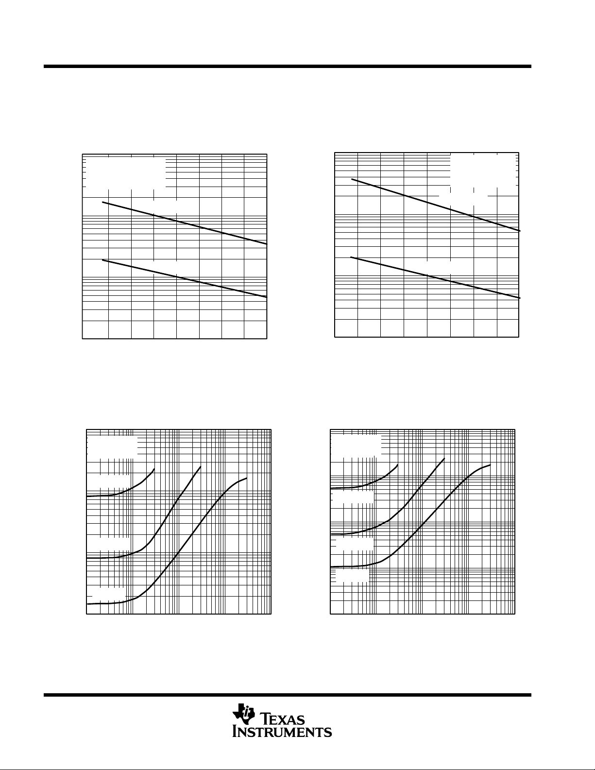
TLV225x, TLV225xA
Advanced LinCMOS RAIL-TO-RAIL
VERY LOW-POWER OPERATIONAL AMPLIFIERS
SLOS185C – FEBRUARY 1997 – REVISED – MARCH 2001
TYPICAL CHARACTERISTICS
LARGE-SIGNAL DIFFERENTIAL
VOLTAGE AMPLIFICATION
vs
FREE-AIR TEMPERATURE
4
10
VDD = 3 V
VIC = 1.5 V
VO = 0.5 V to 2.5 V
3
10
2
10
Amplification – V/mV
– Large-Signal Differential Voltage
VD
A
1
10
–75 125
–50 –25 0 25 50 75 100
TA – Free-Air Temperature – °C
RL = 1 MΩ
RL = 50 kΩ
Figure 28
†‡
Amplification – V/mV
– Large-Signal Differential Voltage
VD
A
10
10
10
10
LARGE-SIGNAL DIFFERENTIAL
VOLTAGE AMPLIFICATION
vs
FREE-AIR TEMPERATURE
4
3
2
1
–50 –25 0 25 50 75 100 125
–75
TA – Free-Air Temperature – °C
RL = 50 kΩ
VDD = 5 V
VIC = 2.5 V
VO = 1 V to 4 V
RL = 1 MΩ
Figure 29
†‡
10
‡
OUTPUT IMPEDANCE
vs
FREQUENCY
1000
VDD = 5 V
TA = 25°C
100
Ω
AV = 100
10
AV = 10
– Output Impedance –
1
o
z
5
10
6
0.1
10
AV = 1
2
3
10
f– Frequency – Hz
10
4
Figure 31
OUTPUT IMPEDANCE
vs
FREQUENCY
1000
VDD = 3 V
TA = 25°C
100
Ω
– Output Impedance –
o
z
10
0.1
1
10
AV = 100
AV = 10
AV = 1
2
3
10
f– Frequency – Hz
10
4
Figure 30
†
Data at high and low temperatures are applicable only within the rated operating free-air temperature ranges of the various devices.
‡
For all curves where VDD = 5 V, all loads are referenced to 2.5 V. For all curves where VDD = 3 V, all loads are referenced to 1.5 V.
10
‡
5
10
6
30
POST OFFICE BOX 655303 • DALLAS, TEXAS 75265
Page 31
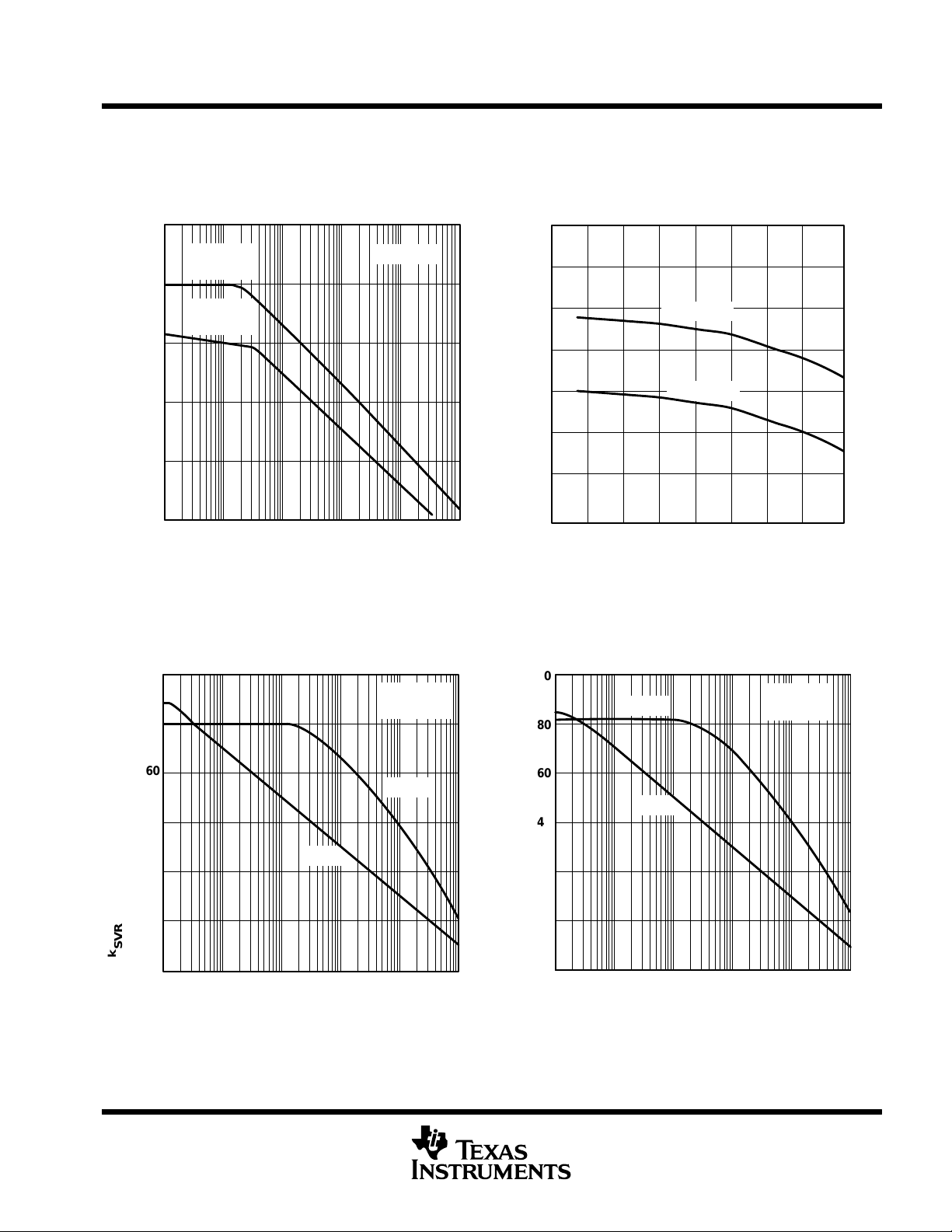
Advanced LinCMOS RAIL-TO-RAIL
VERY LOW-POWER OPERATIONAL AMPLIFIERS
SLOS185C – FEBRUARY 1997 – REVISED – MARCH 2001
TYPICAL CHARACTERISTICS
TLV225x, TLV225xA
CMRR – Common-Mode Rejection Ratio – dB
COMMON-MODE REJECTION RATIO
vs
FREQUENCY
100
VDD = 5 V
VIC = 2.5 V
80
VDD = 3 V
VIC = 1.5 V
60
40
20
0
10
1
2
10
10
f – Frequency – Hz
3
Figure 32
10
4
TA = 25°C
5
10
†
COMMON-MODE REJECTION RATIO
†‡
vs
FREE-AIR TEMPERATURE
94
92
10
90
88
86
84
82
CMMR – Common-Mode Rejection Ratio – dB
6
80
– 75 125
– 50 – 25 0 25 50 75 100
TA – Free-Air Temperature – °C
VDD = 5 V
VDD = 3 V
Figure 33
– Supply-Voltage Rejection Ratio – dB
SVR
k
SUPPLY-VOLTAGE REJECTION RATIO
vs
FREQUENCY
100
80
60
40
k
10
3
SVR–
10
20
–20
0
10
1
2
10
f – Frequency – Hz
Figure 34
4
VDD = 3 V
TA = 25°C
k
SVR+
5
10
†
SUPPLY-VOLTAGE REJECTION RATIO
†
vs
FREQUENCY
100
10
k
SVR+
80
60
k
40
20
– Supply-Voltage Rejection Ratio – dB
0
SVR
k
–20
6
10
1
SVR–
2
10
f – Frequency – Hz
10
3
10
4
VDD = 5 V
TA = 25°C
5
10
10
6
Figure 35
†
For all curves where VDD = 5 V, all loads are referenced to 2.5 V. For all curves where VDD = 3 V, all loads are referenced to 1.5 V.
‡
Data at high and low temperatures are applicable only within the rated operating free-air temperature ranges of the various devices.
POST OFFICE BOX 655303 • DALLAS, TEXAS 75265
31
Page 32

TLV225x, TLV225xA
Á
Advanced LinCMOS RAIL-TO-RAIL
VERY LOW-POWER OPERATIONAL AMPLIFIERS
SLOS185C – FEBRUARY 1997 – REVISED – MARCH 2001
TYPICAL CHARACTERISTICS
– Supply-Voltage Rejection Ratio – dB
SVR
k
SUPPLY-VOLTAGE REJECTION RATIO
vs
FREE-AIR TEMPERATURE
110
VDD = 2.7 V to 8 V
VIC = VO = VDD /2
105
100
95
90
–50 –25 0 25 50 75 100
TA – Free-Air Temperature – °C
Figure 36
†
TLV2252
SUPPLY CURRENT
†
vs
SUPPLY VOLTAGE
120
VO = 0
No Load
100
Aµ
80
60
TA = 25°C
– Supply Current –
40
DD
I
20
125–75
0
012345
VDD – Supply Voltage – V
TA = –40°C
TA = 85°C
678
Figure 37
TLV2254
SUPPLY CURRENT
†
SLEW RATE
vs
SUPPLY VOLTAGE
240
VO = 0
No Load
200
Aµ
160
120
– Supply Current –
80
DD
I
40
0
012345
| V
| – Supply Voltage – V
DD±
TA = –40°C
TA = 85°C
TA = 25°C
678
0.2
VDD = 5 V
AV = –1
0.18
TA = 25°C
0.16
sµ
0.14
V/
0.12
0.1
0.08
SR – Slew Rate –
0.06
0.04
0.02
0
1
10
Figure 38
†
Data at high and low temperatures are applicable only within the rated operating free-air temperature ranges of the various devices.
‡
For all curves where VDD = 5 V, all loads are referenced to 2.5 V. For all curves where VDD = 3 V, all loads are referenced to 1.5 V.
LOAD CAPACITANCE
2
10
CL – Load Capacitance – pF
Figure 39
vs
‡
SR–
SR+
3
10
10
4
32
POST OFFICE BOX 655303 • DALLAS, TEXAS 75265
Page 33

Advanced LinCMOS RAIL-TO-RAIL
VERY LOW-POWER OPERATIONAL AMPLIFIERS
SLOS185C – FEBRUARY 1997 – REVISED – MARCH 2001
TYPICAL CHARACTERISTICS
TLV225x, TLV225xA
SLEW RATE
†‡
vs
FREE-AIR TEMPERATURE
0.2
0.16
sµ
V/
0.12
SR+
0.08
SR – Slew Rate –
0.04
0
–50 –25 0 25 50 75 100
–75 125
TA – Free-Air Temperature – °C
VDD = 5 V
RL = 50 kΩ
CL = 100 pF
AV = 1
SR–
Figure 40
INVERTING LARGE-SIGNAL PULSE
RESPONSE
5
VDD = 5 V
RL = 50 kΩ
CL = 100 pF
4
AV = –1
TA = 25°C
3
†
INVERTING LARGE-SIGNAL PULSE
3
VDD = 3 V
RL = 50 kΩ
CL = 100 pF
2.5
AV = –1
TA = 25°C
2
1.5
1
– Output Voltage – V
O
V
0.5
0
0 102030405060
Figure 41
VOLTAGE-FOLLOWER LARGE-SIGNAL
PULSE RESPONSE
3
VDD = 3 V
RL = 50 kΩ
CL = 100 pF
2.5
AV = 1
TA = 25°C
2
RESPONSE
t – Time – µs
†
70 80 90 100
†
1.5
2
– Output Voltage – V
O
V
1
0
0 102030405060
t – Time – µs
70 80 90 100
Figure 42
†
Data at high and low temperatures are applicable only within the rated operating free-air temperature ranges of the various devices.
‡
For all curves where VDD = 5 V, all loads are referenced to 2.5 V. For all curves where VDD = 3 V, all loads are referenced to 1.5 V.
POST OFFICE BOX 655303 • DALLAS, TEXAS 75265
– Output Voltage – V
1
O
V
0.5
0
0 102030405060
Figure 43
70 80 90 100
t – Time – µs
33
Page 34

TLV225x, TLV225xA
Advanced LinCMOS RAIL-TO-RAIL
VERY LOW-POWER OPERATIONAL AMPLIFIERS
SLOS185C – FEBRUARY 1997 – REVISED – MARCH 2001
TYPICAL CHARACTERISTICS
VOLTAGE-FOLLOWER LARGE-SIGNAL
PULSE RESPONSE
5
VDD = 5 V
RL = 50 kΩ
CL = 100 pF
4
AV = 1
TA = 25°C
3
2
– Output Voltage – V
O
V
1
0
0 102030405060
Figure 44
INVERTING SMALL-SIGNAL
PULSE RESPONSE
2.65
VDD = 5 V
RL = 50 kΩ
CL = 100 pF
2.6
AV = –1
TA = 25°C
t – Time – µs
†
70 80 90 100
†
INVERTING SMALL-SIGNAL
PULSE RESPONSE
0.95
VDD = 3 V
RL = 50 kΩ
0.9
CL = 100 pF
AV = –1
0.85
0.75
– Output Voltage – V
O
V
0.65
TA = 25°C
0.8
0.7
0.6
0102030
t – Time – µs
Figure 45
VOLTAGE-FOLLOWER SMALL-SIGNAL
PULSE RESPONSE
0.95
0.85
0.9
VDD = 3 V
RL = 50 kΩ
CL = 100 pF
AV = 1
TA = 25°C
†
40 50
†
2.55
2.5
O
V
VO – Output Voltage – V
2.45
2.4
0102030
t – Time – µs
40 50
Figure 46
†
For all curves where VDD = 5 V, all loads are referenced to 2.5 V. For all curves where VDD = 3 V, all loads are referenced to 1.5 V.
34
POST OFFICE BOX 655303 • DALLAS, TEXAS 75265
0.8
0.75
O
0.7
V
VO – Output Voltage – V
0.65
0.6
0102030
t – Time – µs
Figure 47
40 50
Page 35

Advanced LinCMOS RAIL-TO-RAIL
VERY LOW-POWER OPERATIONAL AMPLIFIERS
SLOS185C – FEBRUARY 1997 – REVISED – MARCH 2001
TYPICAL CHARACTERISTICS
TLV225x, TLV225xA
VOLTAGE-FOLLOWER SMALL-SIGNAL
PULSE RESPONSE
2.65
VDD = 5 V
RL = 50 kΩ
CL = 100 pF
2.6
AV = 1
TA = 25°C
2.55
2.5
O
V
VO – Output Voltage – V
2.45
2.4
0102030
t – Time – µs
Figure 48
EQUIVALENT INPUT NOISE VOLTAGE
FREQUENCY
60
50
VDD = 5 V
RS = 20 Ω
TA = 25°C
Hz
nV/
vs
†
40 50
EQUIVALENT INPUT NOISE VOLTAGE
†
vs
FREQUENCY
60
VDD = 3 V
RS = 20 Ω
50
40
30
20
10
0
10
TA = 25°C
1
2
10
f – Frequency – Hz
10
3
10
4
nV/ Hz
– Equivalent Input Noise Voltage –
n
V
Figure 49
†
1000
VDD = 5 V
f = 0.1 Hz to 10 Hz
750
TA = 25°C
500
INPUT NOISE VOLTAGE OVER
A 10-SECOND PERIOD
†
40
30
20
10
– Equivalent Input Noise Voltage –
n
V
0
10
1
2
10
f – Frequency – Hz
10
3
10
4
Figure 50
†
For all curves where VDD = 5 V, all loads are referenced to 2.5 V. For all curves where VDD = 3 V, all loads are referenced to 1.5 V.
POST OFFICE BOX 655303 • DALLAS, TEXAS 75265
250
0
–250
Noise Voltage – nV
–500
–750
–1000
0246
t – Time – s
Figure 51
810
35
Page 36

TLV225x, TLV225xA
Advanced LinCMOS RAIL-TO-RAIL
VERY LOW-POWER OPERATIONAL AMPLIFIERS
SLOS185C – FEBRUARY 1997 – REVISED – MARCH 2001
TYPICAL CHARACTERISTICS
10
†
TOTAL HARMONIC DISTORTION PLUS NOISE
vs
FREQUENCY
1
AV = 100
0.1
AV = 10
0.01
0.001
4
10
5
THD + N – Total Harmonic Distortion Plus Noise – %
10
1
AV = 1
2
10
f – Frequency – Hz
10
VDD = 5 V
RL = 50 kΩ
TA = 25°C
3
10
4
Figure 53
GAIN-BANDWIDTH PRODUCT
vs
FREE-AIR TEMPERATURE
300
260
†‡
VDD = 5 V
f = 10 kHz
RL = 50 kHz
CL = 100 pF
INTEGRATED NOISE VOLTAGE
vs
FREQUENCY
100
Calculated Using Ideal Pass-Band Filter
Low Frequency = 1 Hz
Vµ
Integrated Noise Voltage –
TA = 25°C
10
1
0.1
110110
2
f – Frequency – Hz
10
3
Figure 52
GAIN-BANDWIDTH PRODUCT
vs
SUPPLY VOLTAGE
220
210
10
†
5
Gain-Bandwidth Product – kHz
220
180
140
100
–50 –25 0 25 50 10075
TA – Free-Air Temperature – °C
Figure 55
200
190
Gain-Bandwidth Product – kHz
180
170
146
0235
VDD – Supply Voltage – V
78
Figure 54
†
For all curves where VDD = 5 V, all loads are referenced to 2.5 V. For all curves where VDD = 3 V, all loads are referenced to 1.5 V.
36
POST OFFICE BOX 655303 • DALLAS, TEXAS 75265
125–75
Page 37

Advanced LinCMOS RAIL-TO-RAIL
VERY LOW-POWER OPERATIONAL AMPLIFIERS
SLOS185C – FEBRUARY 1997 – REVISED – MARCH 2001
TYPICAL CHARACTERISTICS
TLV225x, TLV225xA
75°
TA = 25°C
60°
45°
30°
m
om – Phase Margin
φ
15°
V
I
0°
1
10
200
TA = 25°C
175
PHASE MARGIN
vs
LOAD CAPACITANCE
R
= 100 Ω
null
R
= 50 Ω
null
R
= 10 Ω
null
50 kΩ
V
50 kΩ
DD+
R
null
–
+
V
DD–
10
CL – Load Capacitance – pF
C
2
Figure 56
UNITY-GAIN BANDWIDTH
vs
LOAD CAPACITANCE
GAIN MARGIN
vs
LOAD CAPACITANCE
Gain Margin – dB
20
15
10
5
0
10
R
= 500 Ω
null
R
= 200 Ω
null
R
= 100 Ω
null
R
= 50 Ω
null
R
= 10 Ω
null
R
= 0
null
TA = 25°C
1
2
10
CL – Load Capacitance – pF
10
3
10
4
10
5
R
= 200 Ω
null
R
= 500 Ω
null
R
= 0
null
L
10
3
10
4
Figure 57
OVERESTIMATION OF PHASE MARGIN
vs
LOAD CAPACITANCE
25
TA = 25°C
R
= 500 Ω
null
20
†
150
125
100
75
50
– Unity-Gain Bandwidth – kHz
1
B
25
0
10
1
2
10
CL – Load Capacitance – pF
10
3
10
4
10
5
Figure 58
†
For all curves where VDD = 5 V, all loads are referenced to 2.5 V. For all curves where VDD = 3 V, all loads are referenced to 1.5 V.
‡
Data at high and low temperatures are applicable only within the rated operating free-air temperature ranges of the various devices.
POST OFFICE BOX 655303 • DALLAS, TEXAS 75265
15
R
= 100 Ω
null
10
R
= 50 Ω
null
R
= 10 Ω
null
5
Overestimation of Phase Margin
0
1
10
†
See application information
2
10
CL – Load Capacitance – pF
Figure 59
10
R
= 200 Ω
null
3
10
4
10
5
37
Page 38

TLV225x, TLV225xA
Advanced LinCMOS RAIL-TO-RAIL
VERY LOW-POWER OPERATIONAL AMPLIFIERS
SLOS185C – FEBRUARY 1997 – REVISED – MARCH 2001
APPLICATION INFORMATION
driving large capacitive loads
The TLV2252 is designed to drive larger capacitive loads than most CMOS operational amplifiers. Figure 56
and Figure 57 illustrate its ability to drive loads up to 1000 pF while maintaining good gain and phase margins
(R
= 0).
null
A smaller series resistor (R
when driving large capacitive loads. Figure 55 and Figure 56 show the effects of adding series resistances of
10 Ω, 50 Ω, 100 Ω, 200 Ω, and 500 Ω. The addition of this series resistor has two effects: the first adds a zero
to the transfer function and the second reduces the frequency of the pole associated with the output load in the
transfer function.
The zero introduced to the transfer function is equal to the series resistance times the load capacitance. To
calculate the improvement in phase margin, equation 1 can be used.
) at the output of the device (see Figure 60) improves the gain and phase margins
null
∆φ
m1
+
tan
–1
ǒ
2 ×π×UGBW × R
null
× C
Ǔ
L
(1)
Where :
∆φm1+
improvement in phase margin
UGBW+unity-gain bandwidth frequency
+
R
null
C
output series resistance
+
load capacitance
L
The unity-gain bandwidth (UGBW) frequency decreases as the capacitive load increases (see Figure 58). To
use equation 1, UGBW must be approximated from Figure 58.
Using equation 1 alone overestimates the improvement in phase margin as illustrated in Figure 59. The
overestimation is caused by the decrease in the frequency of the pole associated with the load, providing
additional phase shift and reducing the overall improvement in phase margin.
Using Figure 60, with equation 1 enables the designer to choose the appropriate output series resistance to
optimize the design of circuits driving large capacitance loads.
50 kΩ
V
DD+
50 kΩ
V
I
–
+
V
DD–
/GND
R
null
C
L
38
Figure 60. Series-Resistance Circuit
POST OFFICE BOX 655303 • DALLAS, TEXAS 75265
Page 39

TLV225x, TLV225xA
Advanced LinCMOS RAIL-TO-RAIL
VERY LOW-POWER OPERATIONAL AMPLIFIERS
SLOS185C – FEBRUARY 1997 – REVISED – MARCH 2001
APPLICATION INFORMATION
macromodel information
Macromodel information provided was derived using Microsim Parts, the model generation software used
with Microsim PSpice. The Boyle macromodel (see Note 5) and subcircuit in Figure 61 are generated using
the TLV2252 typical electrical and operating characteristics at T
simulations of the following key parameters can be generated to a tolerance of 20% (in most cases):
D
Maximum positive output voltage swing
D
Maximum negative output voltage swing
D
Slew rate
D
Quiescent power dissipation
D
Input bias current
D
Open-loop voltage amplification
D
D
D
D
D
D
= 25°C. Using this information, output
A
Unity-gain frequency
Common-mode rejection ratio
Phase margin
DC output resistance
AC output resistance
Short-circuit output current limit
NOTE 5: G. R. Boyle, B. M. Cohn, D. O. Pederson, and J. E. Solomon, “Macromodeling of Integrated Circuit Operational Amplifiers,” IEEE Journal
of Solid-State Circuits, SC-9, 353 (1974).
V
CC+
RSS ISS
RP
2
IN –
DP
IN+
1
V
CC–
.SUBCKT TLV225x 1 2 3 4 5
C1 11 12 6.369E–12
C2 6 7 25.00E–12
DC 5 53 DX
DE 54 5 DX
DLP 90 91 DX
DLN 92 90 DX
DP 43DX
EGND 99 0 POLY (2) (3,0) (4,0) 0 .5 .5
FB 7 99 POLY (5) VB VC VE VLP
+ VLN 0 57.62E6 –60E6 60E6 60E6 –60E6
GA 6 0 1 1 12 26.86E–6
GCM 0 6 10 99 2.686E–9
ISS 3 10 DC 3.1E–6
HLIM 90 0 VLIM 1K
J1 11 2 10 JX
J2 12 1 10 JX
R2 6 9 100.0E3
11
RD1
VAD
10
J1 J2
+
–
99
3
+
VC
12
C1
RD2
60
4
VE
DC
DE
54
+–
R2
–
53
6
GCM
9
EGND
+
FB
+
–
–
VB
C2
GA
RD1 60 11 37.23E3
RD2 60 12 37.23E3
R01 8 5 84
R02 7 99 84
RP 3 4 71.43E3
RSS 10 99 64.52E6
VAD 60 4 –.5
VB 9 0 DC 0
VC 3 53 DC .605
VE 54 4 DC .605
VLIM 7 8 DC 0
VLP 91 0 DC –0.235
VLN 0 92 DC 7.5
.MODEL DX D (IS=800.0E–18)
.MODEL JX PJF (IS=500.0E–15 BETA=139E–6
+ VTO=–.05)
.ENDS
7
VLIM
RO2
HLIM
8
5
OUT
90
+
–
RO1
+
DLP
–
+
–
91
DLN
92
–
VLNVLP
+
Figure 61. Boyle Macromodel and Subcircuit
PSpice and Parts are trademarks of MicroSim Corporation.
POST OFFICE BOX 655303 • DALLAS, TEXAS 75265
39
Page 40

TLV225x, TLV225xA
Advanced LinCMOS RAIL-TO-RAIL
VERY LOW-POWER OPERATIONAL AMPLIFIERS
SLOS185C – FEBRUARY 1997 – REVISED – MARCH 2001
MECHANICAL INFORMATION
D (R-PDSO-G**) PLASTIC SMALL-OUTLINE PACKAGE
14 PIN SHOWN
0.050 (1,27)
14
1
0.069 (1,75) MAX
A
0.020 (0,51)
0.014 (0,35)
0.010 (0,25)
0.004 (0,10)
DIM
8
7
PINS **
0.010 (0,25)
0.157 (4,00)
0.150 (3,81)
M
0.244 (6,20)
0.228 (5,80)
Seating Plane
0.004 (0,10)
8
14
0.008 (0,20) NOM
0°–8°
16
Gage Plane
0.010 (0,25)
0.044 (1,12)
0.016 (0,40)
A MAX
A MIN
NOTES: A. All linear dimensions are in inches (millimeters).
40
B. This drawing is subject to change without notice.
C. Body dimensions do not include mold flash or protrusion, not to exceed 0.006 (0,15).
D. Falls within JEDEC MS-012
POST OFFICE BOX 655303 • DALLAS, TEXAS 75265
0.197
(5,00)
0.189
(4,80)
0.344
(8,75)
0.337
(8,55)
0.394
(10,00)
0.386
(9,80)
4040047/D 10/96
Page 41

TLV225x, TLV225xA
Advanced LinCMOS RAIL-TO-RAIL
VERY LOW-POWER OPERATIONAL AMPLIFIERS
SLOS185C – FEBRUARY 1997 – REVISED – MARCH 2001
MECHANICAL INFORMATION
FK (S-CQCC-N**) LEADLESS CERAMIC CHIP CARRIER
28 TERMINAL SHOWN
A SQ
B SQ
20
22
23
24
25
19
21
12826 27
121314151618 17
0.020 (0,51)
0.010 (0,25)
MIN
0.342
(8,69)
0.442
0.640
0.739
0.938
1.141
A
0.358
(9,09)
0.458
(11,63)
0.660
(16,76)
0.761
(19,32)(18,78)
0.962
(24,43)
1.165
(29,59)
NO. OF
TERMINALS
**
11
10
9
8
7
6
5
432
20
28
44
52
68
84
0.020 (0,51)
0.010 (0,25)
(11,23)
(16,26)
(23,83)
(28,99)
MINMAX
0.307
(7,80)
0.406
(10,31)
0.495
(12,58)
0.495
(12,58)
0.850
(21,6)
1.047
(26,6)
0.080 (2,03)
0.064 (1,63)
B
MAX
0.358
(9,09)
0.458
(11,63)
0.560
(14,22)
0.560
(14,22)
0.858
(21,8)
1.063
(27,0)
0.055 (1,40)
0.045 (1,14)
0.028 (0,71)
0.022 (0,54)
0.050 (1,27)
NOTES: A. All linear dimensions are in inches (millimeters).
B. This drawing is subject to change without notice.
C. This package can be hermetically sealed with a metal lid.
D. The terminals are gold plated.
E. Falls within JEDEC MS-004
POST OFFICE BOX 655303 • DALLAS, TEXAS 75265
0.045 (1,14)
0.035 (0,89)
0.045 (1,14)
0.035 (0,89)
4040140/D 10/96
41
Page 42
TLV225x, TLV225xA
Advanced LinCMOS RAIL-TO-RAIL
VERY LOW-POWER OPERATIONAL AMPLIFIERS
SLOS185C – FEBRUARY 1997 – REVISED – MARCH 2001
MECHANICAL INFORMATION
J (R-GDIP-T**) CERAMIC DUAL-IN-LINE PACKAGE
14 PIN SHOWN
14
1
B
0.100 (2,54)
0.070 (1,78)
0.065 (1,65)
0.045 (1,14)
8
C
7
0.020 (0,51) MIN
0.200 (5,08) MAX
PINS **
DIM
A MAX
A MIN
B MAX
B MIN
C MAX
C MIN
Seating Plane
0.310
(7,87)
0.290
(7,37)
0.785
(19,94)
0.755
(19,18)
0.280
(7,11)
0.245
(6,22)
0.310
(7,87)
0.290
(7,37)
0.785
(19,94)
0.755
(19,18)
0.300
(7,62)
0.245
(6,22)
0.310
(7,87)
0.290
(7,37)
0.910
(23,10)
0.300
(7,62)
0.245
(6,22)
A
20181614
0.310
(7,87)
0.290
(7,37)
0.975
(24,77)
0.930
(23,62)
0.300
(7,62)
0.245
(6,22)
22
0.410
(10,41)
0.390
(9,91)
1.100
(28,00)
0.388
(9,65)
0.130 (3,30) MIN
0.100 (2,54)
0.023 (0,58)
0.015 (0,38)
NOTES: A. All linear dimensions are in inches (millimeters).
B. This drawing is subject to change without notice.
C. This package can be hermetically sealed with a ceramic lid using glass frit.
D. Index point is provided on cap for terminal identification only on press ceramic glass frit seal only.
E. Falls within MIL STD 1835 GDIP1-T14, GDIP1-T16, GDIP1-T18, GDIP1-T20, and GDIP1-T22.
0°–15°
0.014 (0,36)
0.008 (0,20)
4040083/B 04/95
42
POST OFFICE BOX 655303 • DALLAS, TEXAS 75265
Page 43

TLV225x, TLV225xA
Advanced LinCMOS RAIL-TO-RAIL
VERY LOW-POWER OPERATIONAL AMPLIFIERS
SLOS185C – FEBRUARY 1997 – REVISED – MARCH 2001
MECHANICAL INFORMATION
JG (R-GDIP-T8) CERAMIC DUAL-IN-LINE PACKAGE
0.400 (10,20)
0.355 (9,00)
0.063 (1,60)
0.015 (0,38)
0.100 (2,54)
8
1
5
4
0.065 (1,65)
0.045 (1,14)
0.020 (0,51) MIN
0.280 (7,11)
0.245 (6,22)
0.200 (5,08) MAX
0.130 (3,30) MIN
0.023 (0,58)
0.015 (0,38)
0.310 (7,87)
0.290 (7,37)
Seating Plane
0°–15°
0.014 (0,36)
0.008 (0,20)
NOTES: A. All linear dimensions are in inches (millimeters).
B. This drawing is subject to change without notice.
C. This package can be hermetically sealed with a ceramic lid using glass frit.
D. Index point is provided on cap for terminal identification only on press ceramic glass frit seal only.
E. Falls within MIL-STD-1835 GDIP1-T8
POST OFFICE BOX 655303 • DALLAS, TEXAS 75265
4040107/C 08/96
43
Page 44

TLV225x, TLV225xA
Advanced LinCMOS RAIL-TO-RAIL
VERY LOW-POWER OPERATIONAL AMPLIFIERS
SLOS185C – FEBRUARY 1997 – REVISED – MARCH 2001
MECHANICAL INFORMATION
N (R-PDIP-T**) PLASTIC DUAL-IN-LINE PACKAGE
16 PIN SHOWN
16
1
0.035 (0,89) MAX
PINS **
DIM
A
9
0.260 (6,60)
0.240 (6,10)
8
0.070 (1,78) MAX
0.020 (0,51) MIN
0.200 (5,08) MAX
A MAX
A MIN
Seating Plane
14
0.775
(19,69)
0.745
(18,92)
16
0.775
(19,69)
0.745
(18,92)
18
0.920
(23.37)
0.850
(21.59)
20
0.975
(24,77)
0.940
(23,88)
0.310 (7,87)
0.290 (7,37)
0.100 (2,54)
0.021 (0,53)
0.015 (0,38)
NOTES: A. All linear dimensions are in inches (millimeters).
B. This drawing is subject to change without notice.
C. Falls within JEDEC MS-001 (20 pin package is shorter then MS-001.)
0.010 (0,25)
M
0.125 (3,18) MIN
0°–15°
0.010 (0,25) NOM
14/18 PIN ONL Y
4040049/C 08/95
44
POST OFFICE BOX 655303 • DALLAS, TEXAS 75265
Page 45
TLV225x, TLV225xA
Advanced LinCMOS RAIL-TO-RAIL
VERY LOW-POWER OPERATIONAL AMPLIFIERS
SLOS185C – FEBRUARY 1997 – REVISED – MARCH 2001
MECHANICAL INFORMATION
P (R-PDIP-T8) PLASTIC DUAL-IN-LINE PACKAGE
0.400 (10,60)
0.355 (9,02)
58
0.260 (6,60)
0.240 (6,10)
41
0.070 (1,78) MAX
0.020 (0,51) MIN
0.200 (5,08) MAX
0.125 (3,18) MIN
0.100 (2,54)
0.021 (0,53)
0.015 (0,38)
NOTES: A. All linear dimensions are in inches (millimeters).
B. This drawing is subject to change without notice.
C. Falls within JEDEC MS-001
0.010 (0,25)
M
0.310 (7,87)
0.290 (7,37)
Seating Plane
0°–15°
0.010 (0,25) NOM
4040082/B 03/95
POST OFFICE BOX 655303 • DALLAS, TEXAS 75265
45
Page 46
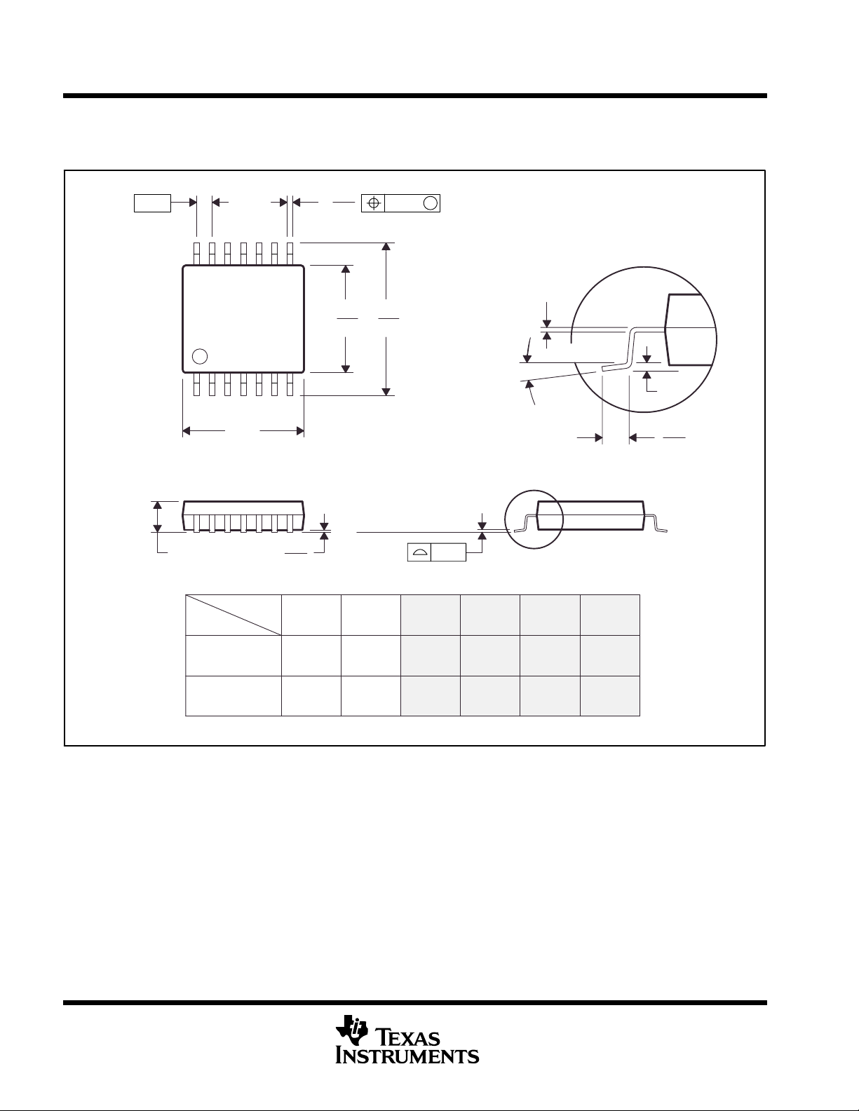
TLV225x, TLV225xA
Advanced LinCMOS RAIL-TO-RAIL
VERY LOW-POWER OPERATIONAL AMPLIFIERS
SLOS185C – FEBRUARY 1997 – REVISED – MARCH 2001
MECHANICAL INFORMATION
PW (R-PDSO-G**) PLASTIC SMALL-OUTLINE PACKAGE
14 PIN SHOWN
0,65
14
1
1,20 MAX
0,30
0,19
8
6,60
4,50
4,30
6,20
7
A
0,15
0,05
M
0,10
Seating Plane
0,10
0,15 NOM
Gage Plane
0,25
0°–8°
0,75
0,50
PINS **
DIM
A MAX
A MIN
NOTES: A. All linear dimensions are in millimeters.
B. This drawing is subject to change without notice.
C. Body dimensions do not include mold flash or protrusion not to exceed 0,15.
D. Falls within JEDEC MO-153
8
3,10
2,90
14
5,10
4,90
16
5,10
20
6,60
6,404,90
24
7,90
7,70
28
9,80
9,60
4040064/E 08/96
46
POST OFFICE BOX 655303 • DALLAS, TEXAS 75265
Page 47
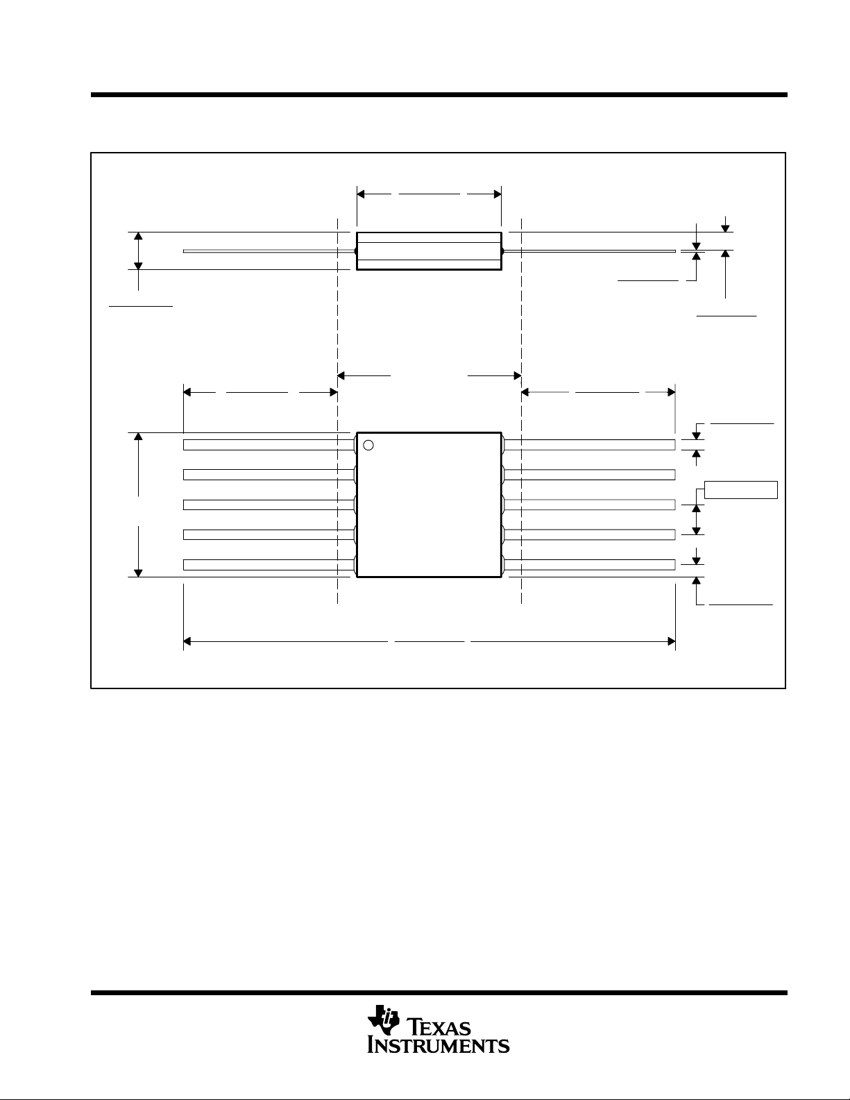
TLV225x, TLV225xA
Advanced LinCMOS RAIL-TO-RAIL
VERY LOW-POWER OPERATIONAL AMPLIFIERS
SLOS185C – FEBRUARY 1997 – REVISED – MARCH 2001
MECHANICAL INFORMATION
U (S-GDFP-F10) CERAMIC DUAL FLATPACK
0.250 (6,35)
0.246 (6,10)
0.006 (0,15)
0.080 (2,03)
0.050 (1,27)
0.004 (0,10)
0.045 (1,14)
0.026 (0,66)
0.250 (6,35)
1
0.250 (6,35)
5
NOTES: A. All linear dimensions are in inches (millimeters).
B. This drawing is subject to change without notice.
C. This package can be hermetically sealed with a ceramic lid using glass frit.
D. Index point is provided on cap for terminal identification only.
E. Falls within MIL STD 1835 GDFP1-F10 and JEDEC MO-092AA
0.300 (7,62)
1.000 (25,40)
0.750 (19,05)
10
0.350 (8,89)0.350 (8,89)
0.250 (6,35)
0.019 (0,48)
0.015 (0,38)
0.050 (1,27)
6
0.025 (0,64)
0.005 (0,13)
4040179/B 03/95
POST OFFICE BOX 655303 • DALLAS, TEXAS 75265
47
Page 48

TLV225x, TLV225xA
Advanced LinCMOS RAIL-TO-RAIL
VERY LOW-POWER OPERATIONAL AMPLIFIERS
SLOS185C – FEBRUARY 1997 – REVISED – MARCH 2001
MECHANICAL INFORMATION
W (R-GDFP-F16) CERAMIC DUAL FLATPACK
0.085 (2,16)
0.045 (1,14)
0.440 (11,18)
0.371 (9,42)
0.285 (7,24)
0.245 (6,22)
0.305 (7,75)
0.355 (9,02) 0.355 (9,02)
0.235 (5,97)
0.275 (6,99)
161
Base and Seating Plane
0.235 (5,97)
0.006 (0,15)
0.004 (0,10)
0.045 (1,14)
0.026 (0,66)
0.019 (0,48)
0.015 (0,38)
0.050 (1,27)
NOTES: A. All linear dimensions are in inches (millimeters).
B. This drawing is subject to change without notice.
C. This package can be hermetically sealed with a ceramic lid using glass frit.
D. Index point is provided on cap for terminal identification only.
E. Falls within MIL-STD-1835 GDFP1-F16 and JEDEC MO-092AC
0.025 (0,64)
0.015 (0,38)
98
1.025 (26,04)
0.745 (18,92)
4040180-3/B 03/95
48
POST OFFICE BOX 655303 • DALLAS, TEXAS 75265
Page 49

PACKAGE OPTION ADDENDUM
www.ti.com
PACKAGING INFORMATION
Orderable Device Status
5962-9550401Q2A ACTIVE LCCC FK 20 1 TBD POST-PLATE Level-NC-NC-NC
5962-9550401QHA ACTIVE CFP U 10 1 TBD A42 SNPB Level-NC-NC-NC
5962-9550401QPA ACTIVE CDIP JG 8 1 TBD A42 SNPB Level-NC-NC-NC
5962-9550403Q2A ACTIVE LCCC FK 20 1 TBD POST-PLATE Level-NC-NC-NC
5962-9550403QHA ACTIVE CFP U 10 1 TBD A42 SNPB Level-NC-NC-NC
5962-9550403QPA ACTIVE CDIP JG 8 1 TBD A42 SNPB Level-NC-NC-NC
TLV2252AID ACTIVE SOIC D 8 75 Green (RoHS &
TLV2252AIDR ACTIVE SOIC D 8 2500 Green (RoHS &
TLV2252AIDRG4 ACTIVE SOIC D 8 2500 Green (RoHS &
TLV2252AIP ACTIVE PDIP P 8 50 Pb-Free
TLV2252AIPE4 ACTIVE PDIP P 8 50 Pb-Free
TLV2252AIPW ACTIVE TSSOP PW 8 150 Green (RoHS &
TLV2252AIPWG4 ACTIVE TSSOP PW 8 150 Green (RoHS &
TLV2252AIPWLE OBSOLETE TSSOP PW 8 TBD Call TI Call TI
TLV2252AIPWR ACTIVE TSSOP PW 8 2000 Green (RoHS &
TLV2252AQD ACTIVE SOIC D 8 75 Pb-Free
TLV2252AQDR ACTIVE SOIC D 8 2500 Pb-Free
TLV2252CP ACTIVE PDIP P 8 TBD Call TI Call TI
TLV2252ID ACTIVE SOIC D 8 75 Green (RoHS &
TLV2252IDG4 ACTIVE SOIC D 8 75 Green (RoHS &
TLV2252IDR ACTIVE SOIC D 8 2500 Green (RoHS &
TLV2252IDRG4 ACTIVE SOIC D 8 2500 Green (RoHS &
TLV2252IP ACTIVE PDIP P 8 50 Pb-Free
TLV2252IPE4 ACTIVE PDIP P 8 50 Pb-Free
TLV2252QD ACTIVE SOIC D 8 75 TBD CU NIPDAU Level-1-220C-UNLIM
TLV2252QDR ACTIVE SOIC D 8 2500 TBD CU NIPDAU Level-1-220C-UNLIM
TLV2254AID ACTIVE SOIC D 14 50 Green (RoHS &
TLV2254AIDG4 ACTIVE SOIC D 14 50 Green (RoHS &
TLV2254AIDR ACTIVE SOIC D 14 2500 Green (RoHS &
(1)
Package
Type
Package
Drawing
Pins Package
Qty
Eco Plan
no Sb/Br)
no Sb/Br)
no Sb/Br)
no Sb/Br)
no Sb/Br)
no Sb/Br)
no Sb/Br)
no Sb/Br)
no Sb/Br)
no Sb/Br)
no Sb/Br)
no Sb/Br)
no Sb/Br)
(RoHS)
(RoHS)
(RoHS)
(RoHS)
(RoHS)
(RoHS)
(2)
Lead/Ball Finish MSL Peak Temp
CU NIPDAU Level-1-260C-UNLIM
CU NIPDAU Level-1-260C-UNLIM
CU NIPDAU Level-1-260C-UNLIM
CU NIPDAU Level-NC-NC-NC
CU NIPDAU Level-NC-NC-NC
CU NIPDAU Level-1-260C-UNLIM
CU NIPDAU Level-1-260C-UNLIM
CU NIPDAU Level-1-260C-UNLIM
CU NIPDAU Level-2-250C-1 YEAR/
CU NIPDAU Level-2-250C-1 YEAR/
CU NIPDAU Level-1-260C-UNLIM
CU NIPDAU Level-1-260C-UNLIM
CU NIPDAU Level-1-260C-UNLIM
CU NIPDAU Level-1-260C-UNLIM
CU NIPDAU Level-NC-NC-NC
CU NIPDAU Level-NC-NC-NC
CU NIPDAU Level-1-260C-UNLIM
CU NIPDAU Level-1-260C-UNLIM
CU NIPDAU Level-1-260C-UNLIM
Level-1-235C-UNLIM
Level-1-235C-UNLIM
13-Sep-2005
(3)
Addendum-Page 1
Page 50

PACKAGE OPTION ADDENDUM
www.ti.com
Orderable Device Status
(1)
Package
Type
Package
Drawing
Pins Package
Qty
Eco Plan
TLV2254AIN ACTIVE PDIP N 14 25 Pb-Free
(2)
Lead/Ball Finish MSL Peak Temp
CU NIPD Level-NC-NC-NC
13-Sep-2005
(3)
(RoHS)
TLV2254AINE4 ACTIVE PDIP N 14 25 Pb-Free
CU NIPD Level-NC-NC-NC
(RoHS)
TLV2254AIPW ACTIVE TSSOP PW 14 90 Green (RoHS &
CU NIPDAU Level-1-260C-UNLIM
no Sb/Br)
TLV2254AIPWG4 ACTIVE TSSOP PW 14 90 Green (RoHS &
CU NIPDAU Level-1-260C-UNLIM
no Sb/Br)
TLV2254AIPWLE OBSOLETE TSSOP PW 14 TBD Call TI Call TI
TLV2254AIPWR ACTIVE TSSOP PW 14 2000 Green (RoHS &
CU NIPDAU Level-1-260C-UNLIM
no Sb/Br)
TLV2254AIPWRG4 ACTIVE TSSOP PW 14 2000 Green (RoHS &
CU NIPDAU Level-1-260C-UNLIM
no Sb/Br)
TLV2254AQD ACTIVE SOIC D 14 50 TBD CU NIPDAU Level-1-220C-UNLIM
TLV2254AQDR ACTIVE SOIC D 14 2500 TBD CU NIPDAU Level-1-220C-UNLIM
TLV2254ID ACTIVE SOIC D 14 50 Green (RoHS &
CU NIPDAU Level-1-260C-UNLIM
no Sb/Br)
TLV2254IDR ACTIVE SOIC D 14 2500 Green (RoHS &
CU NIPDAU Level-1-260C-UNLIM
no Sb/Br)
TLV2254IDRG4 ACTIVE SOIC D 14 2500 Green (RoHS &
CU NIPDAU Level-1-260C-UNLIM
no Sb/Br)
TLV2254IN ACTIVE PDIP N 14 25 Pb-Free
CU NIPD Level-NC-NC-NC
(RoHS)
TLV2254INE4 ACTIVE PDIP N 14 25 Pb-Free
CU NIPD Level-NC-NC-NC
(RoHS)
TLV2254QD ACTIVE SOIC D 14 50 TBD CU NIPDAU Level-1-220C-UNLIM
TLV2254QDR ACTIVE SOIC D 14 2500 TBD CU NIPDAU Level-1-220C-UNLIM
TLV2262AMFKB ACTIVE LCCC FK 20 1 TBD POST-PLATE Level-NC-NC-NC
TLV2262AMJGB ACTIVE CDIP JG 8 1 TBD A42 SNPB Level-NC-NC-NC
TLV2262AMUB ACTIVE CFP U 10 1 TBD A42 SNPB Level-NC-NC-NC
TLV2262MFKB ACTIVE LCCC FK 20 1 TBD POST-PLATE Level-NC-NC-NC
TLV2262MJGB ACTIVE CDIP JG 8 1 TBD A42 SNPB Level-NC-NC-NC
TLV2262MUB ACTIVE CFP U 10 1 TBD A42 SNPB Level-NC-NC-NC
(1)
The marketing status values are defined as follows:
ACTIVE: Product device recommended for new designs.
LIFEBUY: TI has announced that the device will be discontinued, and a lifetime-buy period is in effect.
NRND: Not recommended for new designs. Device is in production to support existing customers, but TI does not recommend using this part in
a new design.
PREVIEW: Device has been announced but is not in production. Samples may or may not be available.
OBSOLETE: TI has discontinued the production of the device.
(2)
Eco Plan - The planned eco-friendly classification: Pb-Free (RoHS) or Green (RoHS & no Sb/Br) - please check
http://www.ti.com/productcontent for the latest availability information and additional product content details.
TBD: The Pb-Free/Green conversion plan has not been defined.
Pb-Free (RoHS): TI's terms "Lead-Free" or "Pb-Free" mean semiconductor products that are compatible with the current RoHS requirements
for all 6 substances, including the requirement that lead not exceed 0.1% by weight in homogeneous materials. Where designed to be soldered
at high temperatures, TI Pb-Free products are suitable for use in specified lead-free processes.
Green (RoHS & no Sb/Br): TI defines "Green" to mean Pb-Free (RoHS compatible), and free of Bromine (Br) and Antimony (Sb) based flame
retardants (Br or Sb do not exceed 0.1% by weight in homogeneous material)
(3)
MSL, Peak Temp. -- The Moisture Sensitivity Level rating according to the JEDEC industry standard classifications, and peak solder
Addendum-Page 2
Page 51

PACKAGE OPTION ADDENDUM
www.ti.com
temperature.
Important Information and Disclaimer:The information provided on this page represents TI's knowledge and belief as of the date that it is
provided. TI bases its knowledge and belief on information provided by third parties, and makes no representation or warranty as to the
accuracy of such information. Efforts are underway to better integrate information from third parties. TI has taken and continues to take
reasonable steps to provide representative and accurate information but may not have conducted destructive testing or chemical analysis on
incoming materials and chemicals. TI and TI suppliers consider certain information to be proprietary, and thus CAS numbers and other limited
information may not be available for release.
In no event shall TI's liability arising out of such information exceed the total purchase price of the TI part(s) at issue in this document sold by TI
to Customer on an annual basis.
13-Sep-2005
Addendum-Page 3
Page 52

MECHANICAL DATA
MCER001A – JANUARY 1995 – REVISED JANUARY 1997
JG (R-GDIP-T8) CERAMIC DUAL-IN-LINE
0.400 (10,16)
0.355 (9,00)
0.063 (1,60)
0.015 (0,38)
0.100 (2,54)
8
1
5
4
0.065 (1,65)
0.045 (1,14)
0.020 (0,51) MIN
0.023 (0,58)
0.015 (0,38)
0.280 (7,11)
0.245 (6,22)
0.310 (7,87)
0.290 (7,37)
0.200 (5,08) MAX
Seating Plane
0.130 (3,30) MIN
0°–15°
0.014 (0,36)
0.008 (0,20)
NOTES: A. All linear dimensions are in inches (millimeters).
B. This drawing is subject to change without notice.
C. This package can be hermetically sealed with a ceramic lid using glass frit.
D. Index point is provided on cap for terminal identification.
E. Falls within MIL STD 1835 GDIP1-T8
4040107/C 08/96
POST OFFICE BOX 655303 • DALLAS, TEXAS 75265
Page 53
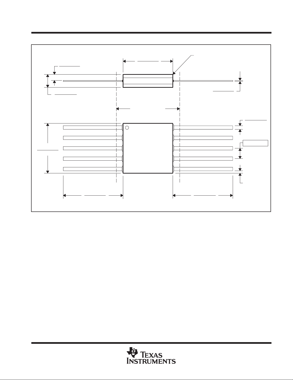
MECHANICAL DATA
MCFP001A – JANUARY 1995 – REVISED DECEMBER 1995
U (S-GDFP-F10) CERAMIC DUAL FLATP ACK
0.280 (7,11)
0.230 (5,84)
0.045 (1,14)
0.026 (0,66)
0.080 (2,03)
0.050 (1,27)
0.250 (6,35)
0.300 (7,62) MAX
1
5
0.250 (6,35)
0.246 (6,10)
10
Base and Seating Plane
0.008 (0,20)
0.004 (0,10)
0.019 (0,48)
0.015 (0,38)
0.050 (1,27)
6
4 Places
0.005 (0,13) MIN
0.350 (8,89)0.350 (8,89)
0.250 (6,35)
NOTES: A. All linear dimensions are in inches (millimeters).
B. This drawing is subject to change without notice.
C. This package can be hermetically sealed with a ceramic lid using glass frit.
D. Index point is provided on cap for terminal identification only.
E. Falls within MIL STD 1835 GDFP1-F10 and JEDEC MO-092AA
4040179/B 03/95
POST OFFICE BOX 655303 • DALLAS, TEXAS 75265
Page 54

MECHANICAL DATA
MLCC006B – OCTOBER 1996
FK (S-CQCC-N**) LEADLESS CERAMIC CHIP CARRIER
28 TERMINAL SHOWN
A SQ
B SQ
20
22
23
24
25
19
21
12826 27
12
1314151618 17
0.020 (0,51)
0.010 (0,25)
MIN
0.342
(8,69)
0.442
0.640
0.739
0.938
1.141
A
0.358
(9,09)
0.458
(11,63)
0.660
(16,76)
0.761
(19,32)(18,78)
0.962
(24,43)
1.165
(29,59)
NO. OF
TERMINALS
**
11
10
9
8
7
6
5
432
20
28
44
52
68
84
0.020 (0,51)
0.010 (0,25)
(11,23)
(16,26)
(23,83)
(28,99)
MINMAX
0.307
(7,80)
0.406
(10,31)
0.495
(12,58)
0.495
(12,58)
0.850
(21,6)
1.047
(26,6)
0.080 (2,03)
0.064 (1,63)
B
MAX
0.358
(9,09)
0.458
(11,63)
0.560
(14,22)
0.560
(14,22)
0.858
(21,8)
1.063
(27,0)
0.055 (1,40)
0.045 (1,14)
0.028 (0,71)
0.022 (0,54)
0.050 (1,27)
NOTES: A. All linear dimensions are in inches (millimeters).
B. This drawing is subject to change without notice.
C. This package can be hermetically sealed with a metal lid.
D. The terminals are gold plated.
E. Falls within JEDEC MS-004
POST OFFICE BOX 655303 • DALLAS, TEXAS 75265
0.045 (1,14)
0.035 (0,89)
0.045 (1,14)
0.035 (0,89)
4040140/D 10/96
Page 55

MECHANICAL DATA
MPDI001A – JANUARY 1995 – REVISED JUNE 1999
P (R-PDIP-T8) PLASTIC DUAL-IN-LINE
0.400 (10,60)
0.355 (9,02)
8
5
0.260 (6,60)
0.240 (6,10)
1
0.021 (0,53)
0.015 (0,38)
NOTES: A. All linear dimensions are in inches (millimeters).
B. This drawing is subject to change without notice.
C. Falls within JEDEC MS-001
4
0.070 (1,78) MAX
0.020 (0,51) MIN
0.200 (5,08) MAX
0.125 (3,18) MIN
0.100 (2,54)
0.010 (0,25)
Seating Plane
M
0.325 (8,26)
0.300 (7,62)
0.015 (0,38)
Gage Plane
0.010 (0,25) NOM
0.430 (10,92)
MAX
4040082/D 05/98
For the latest package information, go to http://www.ti.com/sc/docs/package/pkg_info.htm
POST OFFICE BOX 655303 • DALLAS, TEXAS 75265
Page 56

Page 57

Page 58

Page 59

MECHANICAL DATA
MTSS001C – JANUARY 1995 – REVISED FEBRUARY 1999
PW (R-PDSO-G**) PLASTIC SMALL-OUTLINE PACKAGE
14 PINS SHOWN
0,65
1,20 MAX
14
0,30
0,19
8
4,50
4,30
PINS **
7
Seating Plane
0,15
0,05
8
1
A
DIM
14
0,10
6,60
6,20
M
0,10
0,15 NOM
0°–8°
2016
Gage Plane
24
0,25
0,75
0,50
28
A MAX
A MIN
NOTES: A. All linear dimensions are in millimeters.
B. This drawing is subject to change without notice.
C. Body dimensions do not include mold flash or protrusion not to exceed 0,15.
D. Falls within JEDEC MO-153
3,10
2,90
5,10
4,90
5,10
4,90
6,60
6,40
7,90
7,70
9,80
9,60
4040064/F 01/97
POST OFFICE BOX 655303 • DALLAS, TEXAS 75265
Page 60

IMPORTANT NOTICE
Texas Instruments Incorporated and its subsidiaries (TI) reserve the right to make corrections, modifications,
enhancements, improvements, and other changes to its products and services at any time and to discontinue
any product or service without notice. Customers should obtain the latest relevant information before placing
orders and should verify that such information is current and complete. All products are sold subject to TI’s terms
and conditions of sale supplied at the time of order acknowledgment.
TI warrants performance of its hardware products to the specifications applicable at the time of sale in
accordance with TI’s standard warranty. Testing and other quality control techniques are used to the extent TI
deems necessary to support this warranty . Except where mandated by government requirements, testing of all
parameters of each product is not necessarily performed.
TI assumes no liability for applications assistance or customer product design. Customers are responsible for
their products and applications using TI components. To minimize the risks associated with customer products
and applications, customers should provide adequate design and operating safeguards.
TI does not warrant or represent that any license, either express or implied, is granted under any TI patent right,
copyright, mask work right, or other TI intellectual property right relating to any combination, machine, or process
in which TI products or services are used. Information published by TI regarding third-party products or services
does not constitute a license from TI to use such products or services or a warranty or endorsement thereof.
Use of such information may require a license from a third party under the patents or other intellectual property
of the third party, or a license from TI under the patents or other intellectual property of TI.
Reproduction of information in TI data books or data sheets is permissible only if reproduction is without
alteration and is accompanied by all associated warranties, conditions, limitations, and notices. Reproduction
of this information with alteration is an unfair and deceptive business practice. TI is not responsible or liable for
such altered documentation.
Resale of TI products or services with statements different from or beyond the parameters stated by TI for that
product or service voids all express and any implied warranties for the associated TI product or service and
is an unfair and deceptive business practice. TI is not responsible or liable for any such statements.
Following are URLs where you can obtain information on other Texas Instruments products and application
solutions:
Products Applications
Amplifiers amplifier.ti.com Audio www.ti.com/audio
Data Converters dataconverter.ti.com Automotive www.ti.com/automotive
DSP dsp.ti.com Broadband www.ti.com/broadband
Interface interface.ti.com Digital Control www.ti.com/digitalcontrol
Logic logic.ti.com Military www.ti.com/military
Power Mgmt power.ti.com Optical Networking www.ti.com/opticalnetwork
Microcontrollers microcontroller.ti.com Security www.ti.com/security
Telephony www.ti.com/telephony
Video & Imaging www.ti.com/video
Wireless www.ti.com/wireless
Mailing Address: Texas Instruments
Post Office Box 655303 Dallas, Texas 75265
Copyright 2005, Texas Instruments Incorporated
 Loading...