

Datasheet TLV1562IDW, TLV1562IDWR, TLV1562EVM, TLV1562CPWR, TLV1562CDWR Datasheet (Texas Instruments)
...
TLV1562
2.7 V TO 5.5 V, HIGH-SPEED LOW-POWER RECONFIGURABLE ANALOG-TO-DIGITAL
CONVERTER WITH 4-INPUT, DUAL S/H, PARALLEL INTERFACE, AND POWER DOWN
SLAS162 – SEPTEMBER 1998
1
POST OFFICE BOX 655303 • DALLAS, TEXAS 75265
D
2 MSPS Max Throughput at 10 Bit (Single
Channel), ±1 LSB DNL, ±1 LSB INL MAX
D
3 MSPS Max Throughput at 8 Bit (Single
Channel), ±1 LSB DNL, ±1 LSB INL MAX
D
7 MSPS Max Throughput at 4 Bit (Single
Channel), ±0.4 LSB DNL, ±0.4 LSB INL MAX
D
No Missing Code for External Clock Up to
15 MHz at 5.5 V, 12 MHz at 2.7 V
D
ENOB 9.4 Bit, SINAD 57.8 dB, SFDR
–70.8 dB, THD –68.8 dB, at fi = 800 kHz,
10 Bit
D
Wide Input Bandwidth for Undersampling
(75 MHz at 1 dB, >120 MHz at –3 dB) at
Rs = 1 kΩ
D
Software Programmable Power Down,
(1 µA), Auto Powerdown (120 µA)
D
Single Wide Range Supply 2.7 VDC to
5.5 VDC
D
Low Supply Current 11 mA at 5.5 V, 10 MHz;
7 mA at 2.7 V, 8 MHz Operating
D
Simultaneous Sample and Hold:
Dual Sample and Hold Matched Channels
Multi Chip Simultaneous Sample and Hold
Capable
D
Programmable Conversion Modes:
Interrupt-Driven for Shorter Latency
Continuous Modes Optimized for MIPS
Sensitive DSP Solutions
D
Built-In Internal/System Mid-Scale Error
Calibration
D
Built-In Mux With 2 Differential or 4
Single-Ended Input Channels
D
Low Input Capacitance (10 pF Max Fixed,
1 pF Max Switching)
D
DSP/µ P-Compatible Parallel Interface
applications
D
Portable Digital Radios
D
Personal Communication Assistants
D
Cellular
D
Pager
D
Scanner
D
Digitizers
D
Process Controls
D
Motor Control
D
Remote Sensing
D
Automotive
D
Servo Controls
D
Cameras
1
2
3
4
5
6
7
8
9
10
11
12
13
14
28
27
26
25
24
23
22
21
20
19
18
17
16
15
CSTART
(LSB) D0
D1
D2
D3
D4
BDV
DD
BDGND
D5
D6
D7
D8
(MSB) D9
INT
RD
AP/CH1
AM/CH2
BP/CH3
BM/CH4
AV
DD
VREFP
VREFM
AGND
WR
DGND
DV
DD
CLKIN
CS
/OE
DW OR PW PACKAGE
(TOP VIEW)
Copyright 1998, Texas Instruments Incorporated
PRODUCTION DATA information is current as of publication date.
Products conform to specifications per the terms of Texas Instruments
standard warranty. Production processing does not necessarily include
testing of all parameters.
Please be aware that an important notice concerning availability, standard warranty, and use in critical applications of
Texas Instruments semiconductor products and disclaimers thereto appears at the end of this data sheet.
TLV1562
2.7 V TO 5.5 V, HIGH-SPEED LOW-POWER RECONFIGURABLE ANALOG-TO-DIGITAL
CONVERTER WITH 4-INPUT, DUAL S/H, PARALLEL INTERFACE, AND POWER DOWN
SLAS162 – SEPTEMBER 1998
2
POST OFFICE BOX 655303 • DALLAS, TEXAS 75265
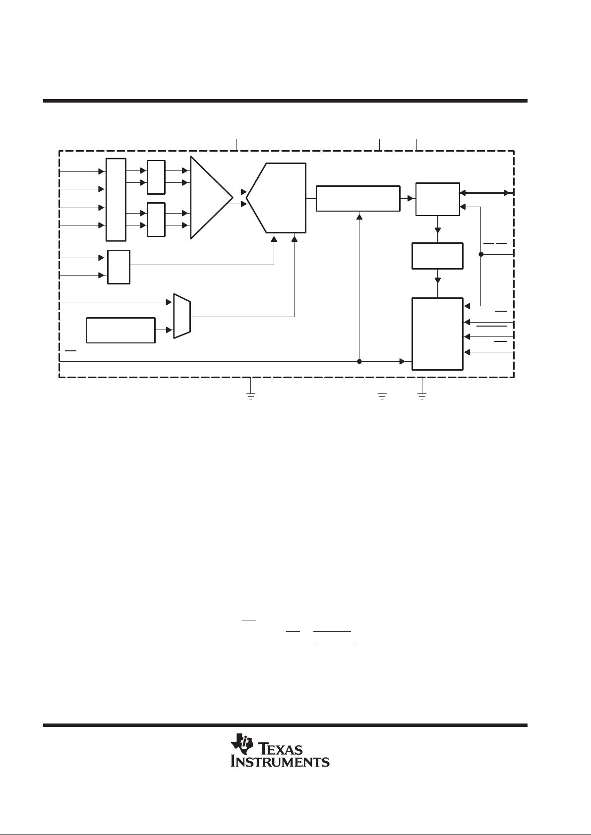
functional block diagram
REF
M
U
X
S/H
4/8/10-Bit
Recyclic
ADC
OSC
(7.5 MHz Min)
Serial/Parallel Conv
and FIFO
3-State
Buffer
Control
Register
Interface
Timing
and
Control
AV
DD
DV
DD
BDV
DD
AGND DGND BDGND
AP/CH1
D (0–9)
CS/OE
INT
CSTART
WR
SysClk
AM/CH2
BP/CH3
BM/CH4
VREFP
VREFM
CLKIN
RD
(15 MHz Max)
VREFMID
S/H
Amplifier
description
The TLV1562 is a 10-bit CMOS low-power, high-speed programmable resolution analog-to-digital converter
based on a low-power recyclic architecture. The unique architecture delivers a throughput up to 2 MSPS (million
samples per second) at 10-bit resolution. The programmable resolution allows a higher conversion throughput
as a tradeoff of lower resolution. A high speed 3-state parallel port directly interfaces to a digital signal processor
(DSP) or microprocessor (µP) system data bus. D0 through D9 are the digital output terminals with D0 being
the least significant bit (LSB). The TLV1562 is designed to operate for a wide range of supply voltages
(2.7 V to 5.5 V) with very low power consumption (1 1 mA maximum at 5.5 V , 10 MHz CLKIN). The power saving
feature is further enhanced with a software power-down feature (1 µA maximum) and auto power-down (1 µA
maximum) feature.
Many programmable features make this device a flexible general-purpose data converter. The device can be
configured as either four single-ended inputs to maximize the capacity or two differential inputs to improve noise
immunity. The internal system clock (SYSCLK) may come from either an internally generated OSC or an
external clock source (CLKIN). Four different modes of conversion are available for different applications. The
interrupt driven modes are mostly suitable for asynchronous applications, while the continuous modes take
advantage of the high speed nature of a pipelined architecture. A pair of built-in sample-and-hold amplifiers
allow simultaneous sampling of two input channels. This makes the TLV1562 perfect for communication
applications. Conversion is started by the RD
signal, which can also be used for reading data, to maximize the
throughput. Conversion can be started either by the RD or CST ART signal when the device is operating in the
interrupt-driven modes. The dedicated conversion start pin, CST ART , provides a mechanism to simultaneously
sample and convert multiple channels when multiple converters are used in an application.
TLV1562
2.7 V TO 5.5 V, HIGH-SPEED LOW-POWER RECONFIGURABLE ANALOG-TO-DIGITAL
CONVERTER WITH 4-INPUT, DUAL S/H, PARALLEL INTERFACE, AND POWER DOWN
SLAS162 – SEPTEMBER 1998
3
POST OFFICE BOX 655303 • DALLAS, TEXAS 75265
description (continued)
The converter incorporates a pair of differential high-impedance reference inputs that facilitate ratiometric
conversion, scaling, and isolation of analog circuitry from logic and supply noise. Other features such as low
input capacitance (10 pF) and very wide input bandwidth (75 MHz) make this device a perfect digital signal
processing (DSP) companion for mobile communication applications. A switched-capacitor design allows
low-error conversion over the full operating free-air temperature range.
The features that make this device truly a DSP friendly converter include: 1) programmable continuous
conversion modes, 2) programmable 2s complement output code format, and 3) programmable resolution. The
TL V1562 is of fered in both 28-pin TSSOP and SOIC packages. The TLV1562C is characterized for operation
from 0°C to 70°C. The TLV1562I is characterized for operation over the full industrial temperature range of
–40°C to 85°C.
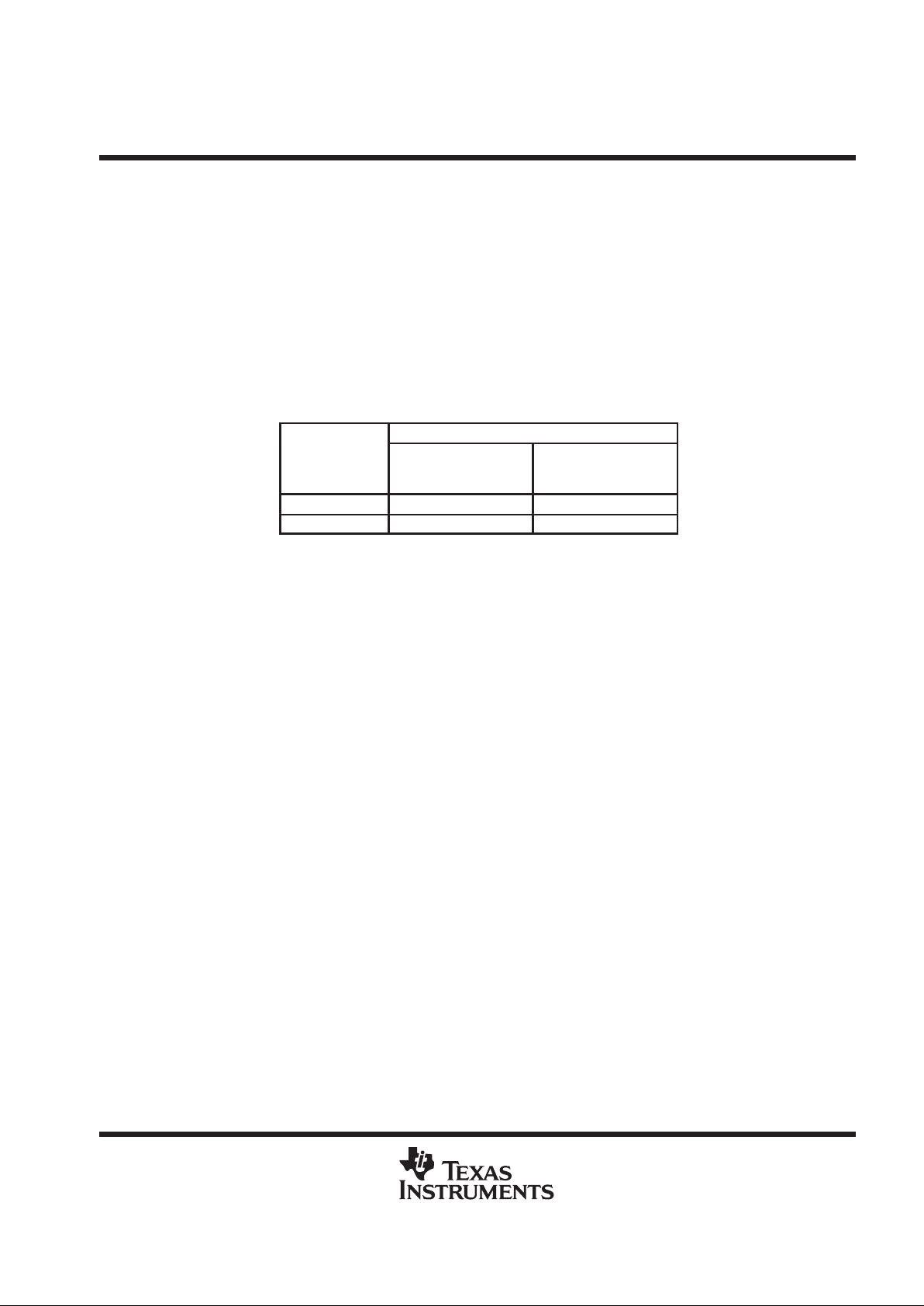
AVAILABLE OPTIONS
PACKAGED DEVICE
T
A
28-TSSOP
(25 MIL PITCH)
(PW)
28-SOIC
(50 MIL PITCH)
(DW)
0°C to 70°C TLV1562CPW TLV1562CDW
–40°C to 85°C TLV1562IPW TLV1562IDW
TLV1562
2.7 V TO 5.5 V, HIGH-SPEED LOW-POWER RECONFIGURABLE ANALOG-TO-DIGITAL
CONVERTER WITH 4-INPUT, DUAL S/H, PARALLEL INTERFACE, AND POWER DOWN
SLAS162 – SEPTEMBER 1998
4
POST OFFICE BOX 655303 • DALLAS, TEXAS 75265
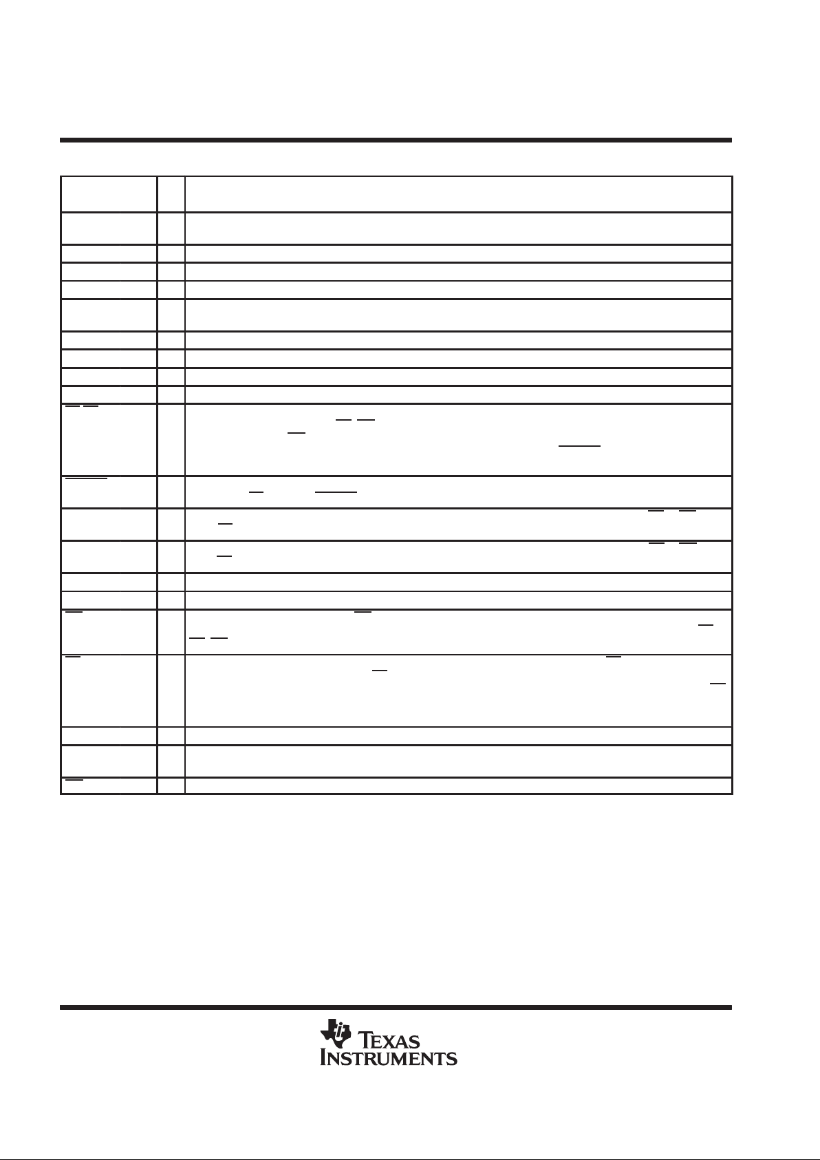
Terminal Functions
TERMINAL
NAME NO.
I/O
DESCRIPTION
AGND 20 I Analog ground return for the internal circuitry. Unless otherwise noted, all analog voltage measurements are with
respect to AGND.
AM/CH2 26 I Differential channel A input minus or single-ended channel 2
AP/CH1 27 I Differential channel A input plus or single-ended channel 1
AV
DD
23 I Positive analog supply voltage
BDGND 8 I Digital ground return for the I/O buffers. Unless otherwise noted, all digital interface voltage measurements are with
respect to DGND.
BDV
DD
7 I Positive digital supply voltage for I/O buffers
BM/CH4 24 I Differential channel B input minus or single-ended channel 4
BP/CH3 25 I Differential channel B input plus or single-ended channel 3
CLKIN 16 I External clock input. (1 MHz to 15 MHz)
CS/OE 15 I Chip select. A high-to-low transition on this input resets the internal counters and controls and enables the output data
bus D(0–9) and control inputs (RD
, WR) within a maximum setup time. A low-to-high transition disables the output
data bus D(9–0) and WR
within a maximum setup time. This signal also serves as an output enable signal when the
device is programmed into both mono and dual interrupt-driven modes using CSTART
as the start of conversion
signal.
CSTART 1 I Conversion start signal. A falling edge starts the sampling period and a rising edge starts the conversion. This signal
acts without CS
activated. CSTAR T connects to DVDD via a 10-kΩ pull-up resistor if not used.
D(0–4) 2–6 I/O The lower bits of the 3-state parallel data bus. Bidirectional. The data bus is 3-stated except when RD or WR is low
when CS
is low.
D(5–9) 9–13 I/O The higher bits of the 3-state parallel data bus. Bidirectional. The data bus is 3-stated except when RD or WR is low
when CS
is low. When the host processor writes to the converter , D(9,8) are used as an index to the internal registers.
DGND 18 I Digital ground return for the internal digital logic circuitry
DV
DD
17 I Positive digital supply voltage
INT 14 O Interrupt output. The falling edge of INT signals the end of conversion. This output goes from a high impedance state
to low logic level on the fifth falling edge of the system clock and remains low until reset by the rising edge of CS
or
RD
. INT requires connection of a 10-kΩ pull-up resistor.
RD 28 I Processor read strobe or synchronous start of conversion/sampling. The falling edge of RD is used to 1) start the
conversion in interrupt-driven mode (if RD
is programmed as the start conversion signal); 2) start both conversion
and next sampling plus release of the previous conversion data in both continuous modes. The rising edge of RD
serves as a read strobe and data is 3-stated (approximately 10 ns at 50 pF bus loading) after this edge. Connection
of a 10-kΩ pull-up resistor is optional.
VREFM 21 I The lower voltage reference value is applied to this terminal.
VREFP 22 I The upper reference voltage value is applied to this terminal. The maximum input voltage range is determined by the
difference between the voltage applied to this terminal and the VREFM terminal.
WR 19 I Processor write strobe. Active low. Connection of a 10-kΩ pull-up resistor is optional.
detailed description
The TL V1562 analog-to-digital converter is based on an advanced low power recyclic architecture. T wo bits of
the conversion result are presented per system clock cycle. A total of 5 system clock (SYSCLK) cycles is
required to complete the conversion. The serial conversion results are converted to a parallel word for output.
The device supports both interrupt-driven (typically found in a SAR type ADC) and continuous (natural for a
pipeline type ADC) modes of conversion. An innovative conversion scheme makes this device perfect for power
sensitive applications with uncompromised speed.
TLV1562
2.7 V TO 5.5 V, HIGH-SPEED LOW-POWER RECONFIGURABLE ANALOG-TO-DIGITAL
CONVERTER WITH 4-INPUT, DUAL S/H, PARALLEL INTERFACE, AND POWER DOWN
SLAS162 – SEPTEMBER 1998
5
POST OFFICE BOX 655303 • DALLAS, TEXAS 75265
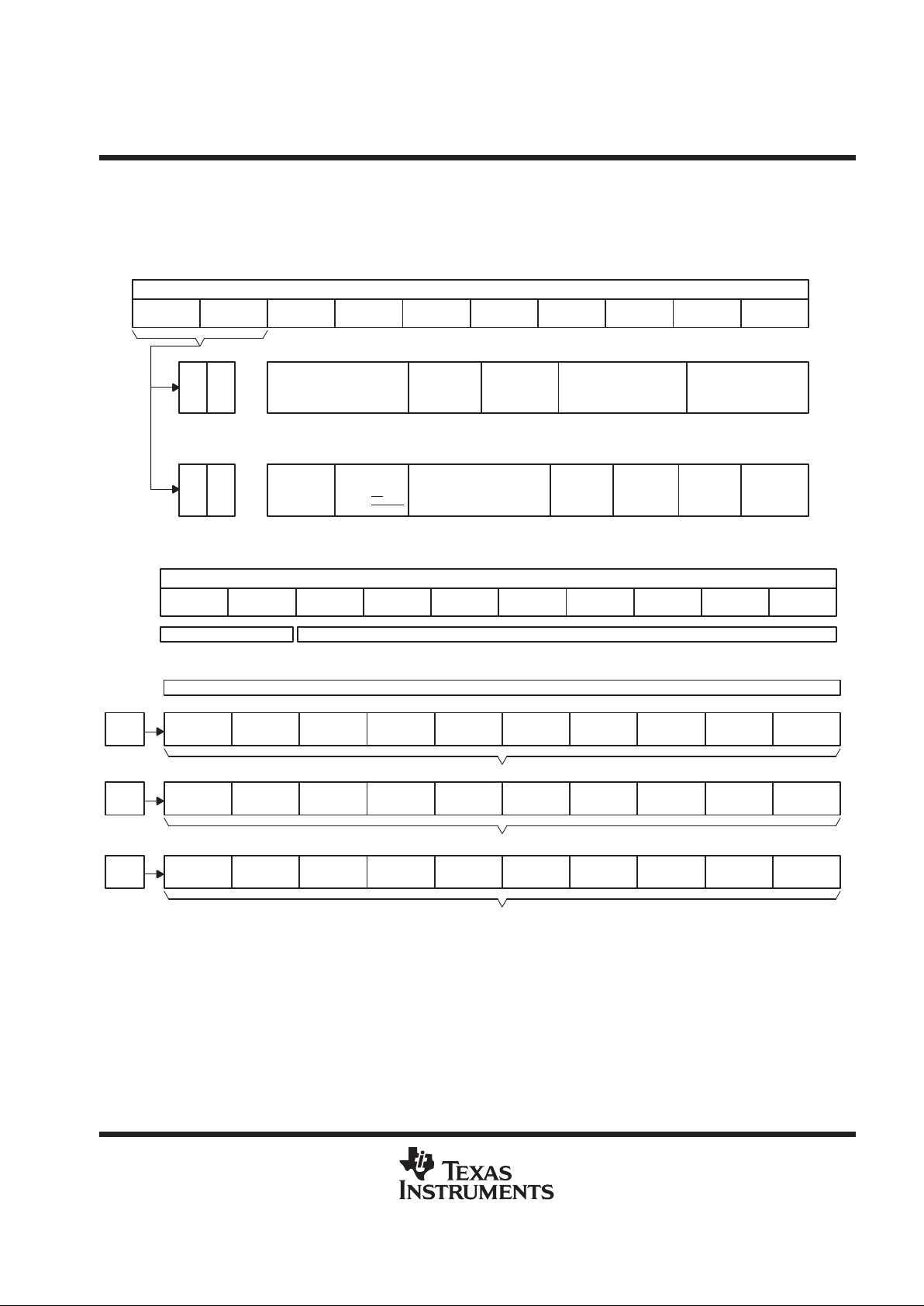
control register
The TL V1562 is software configurable. The first two bits, MSBs (D9,8), are used to address the register set. The
rest of the 8 bits are used as data. There are two control registers, CR0 and CR1, for user configuration. All of
these register bits are written to the control register during a write cycle. A description of the control registers
and the input/output data formats are shown in Figure 1.
Pin D9
Index1
Pin D8
Index0
Pin D7 Pin D6
CR0
0
Offset Calibration Set OMS(1,0)
0,0 = Operate with calibration
0,1 = Measure system offset
1,0 = Measure internal offset
1,1 = Operate without calibration
001
Input Data Format
Pin D9 Pin D8 Pin D7 Pin D6 Pin D5 Pin D4 Pin D3 Pin D2 Pin D1 Pin D0
Output Data Format
10-Bit Conversion Result
4-Bit Conversion Result
8-Bit Conversion Result
CR1
D(5,4)
= 0,0
OD9
OD3
OD7
CR1
MSB
OD8
OD7 OD6 OD5 OD4 OD3 OD2 OD1 OD0
LSB
OD2 OD1 OD0 Z Z Z Z Z Z
OD6 OD5 OD4 OD3 OD2 OD1 OD0 Z Z
MSB LSB
MSB LSB
Conversion
Clock Select
0 = Internal
1 = External
Input Type:
0 = Single end
1 = Differential
Conversion Mode Select MS(1,0)
0,0 = Mono interrupt
0,1 = Dual interrupt
1,0 = Mono continuous
1,1 = Dual continuous
Channel Select CS(1,0)
0,0 = Ch1 or pair A
0,1 = Ch2 or pair A
1,0 = Ch3 or pair B
1,1 = Ch4 or pair B
System Offset Calibration: Short the system input to the system AGND
Internal Offset Calibration: Short the two inputs to the S/HA to AGND
0 Interrupt-Mode
Conversion
Started
0 = By RD
1 = By CSTART
Resolution Select BS(1,0)
0,0 = 10-Bit
0,1 = 4-Bit
1.0 = 8-Bit
1.1 = 12-Bit Test
0 Output Format
0 = 2’s
Complement
1 = Binary
Interrupt-Mode
Auto
Power Down
0 = Disabled
1 = Enabled
SW Power Down
0 = Normal
1 = S/W Power
Down
Register Index Configuration Register Content
Configuration Result
CR1
D(5,4)
= 0,1
CR1
D(5,4)
= 1,0
Reference delta should be greater than 2 V when swing is reduced.
NOTE: Z indicates bits write zero read zero back.
Pin D5 Pin D4 Pin D3 Pin D2 Pin D1 Pin D0
Figure 1. Input/Output Data Formats
NOTE:
Channel select bits CR0.(1,0), CS(1,0) are ignored when the device is in the dual (interrupt or
continuous) modes using differential inputs, since both differential input pairs are automatically
selected. CR0.0 (i.e., CS0 bit) is used to determine if channels 1 and 3 or channels 2 and 4 are
selected if single-ended input mode is used.
TLV1562
2.7 V TO 5.5 V, HIGH-SPEED LOW-POWER RECONFIGURABLE ANALOG-TO-DIGITAL
CONVERTER WITH 4-INPUT, DUAL S/H, PARALLEL INTERFACE, AND POWER DOWN
SLAS162 – SEPTEMBER 1998
6
POST OFFICE BOX 655303 • DALLAS, TEXAS 75265
detailed description (continued)
Table 1. Select Input Channels
CR0.4
(INPUT TYPE)
CR0.(3,2)
(CONVERSION MODE
SELECT)
CR0.(1,0)
(CHANNEL SELECT)
CHANNEL(S)
SELECTED
NOTE
0 (Single-ended) 00 or 10 0,0 CH1 Single channel
0 (Single-ended) 00 or 10 0,1 CH2 Single channel
0 (Single-ended) 00 or 10 1,0 CH3 Single channel
0 (Single-ended) 00 or 10 1,1 CH4 Single channel
1 (Differential) 00 or 10 0,X Differential pair A Single channel
1 (Differential) 00 or 10 1,X Differential pair B Single channel
0 (Single-ended) 01 or 11 X,0 Both CH1 and CH3 Dual channels
0 (Single-ended) 01 or 11 X,1 Both CH2 and CH4 Dual channels
0 (Single-ended) 01 or 11 X,0 Both CH1 and CH3 Dual channels
0 (Single-ended) 01 or 11 X,1 Both CH2 and CH4 Dual channels
1 (Differential) 01 or 11 X,X Both differential pairs A and B Dual channels
configure the device
The device can be configured by writing to control registers CR0 and CR1. A read register is carried out by
auto-sequence when the device is put into the software power-down state. CR0 is read first and then CR1 at
the next two RD rising edges after the device is in the software power-down state. The falling edge of RD has
no meaning and does not trigger a conversion in the software power-down state.
V
IH
V
IL
V
IH
V
IH
V
IL
CS
CSTART
WR
DATA
t
d(CSL-WRL)
t
w(CSH)
t
d(WRH-CSH)
V
IH
V
IL
t
s(DATAIN)
t
w(WRL)
t
h(DATAIN)
Configure Data
Figure 2. Configuration Cycle Timing
TLV1562
2.7 V TO 5.5 V, HIGH-SPEED LOW-POWER RECONFIGURABLE ANALOG-TO-DIGITAL
CONVERTER WITH 4-INPUT, DUAL S/H, PARALLEL INTERFACE, AND POWER DOWN
SLAS162 – SEPTEMBER 1998
7
POST OFFICE BOX 655303 • DALLAS, TEXAS 75265
detailed description (continued)
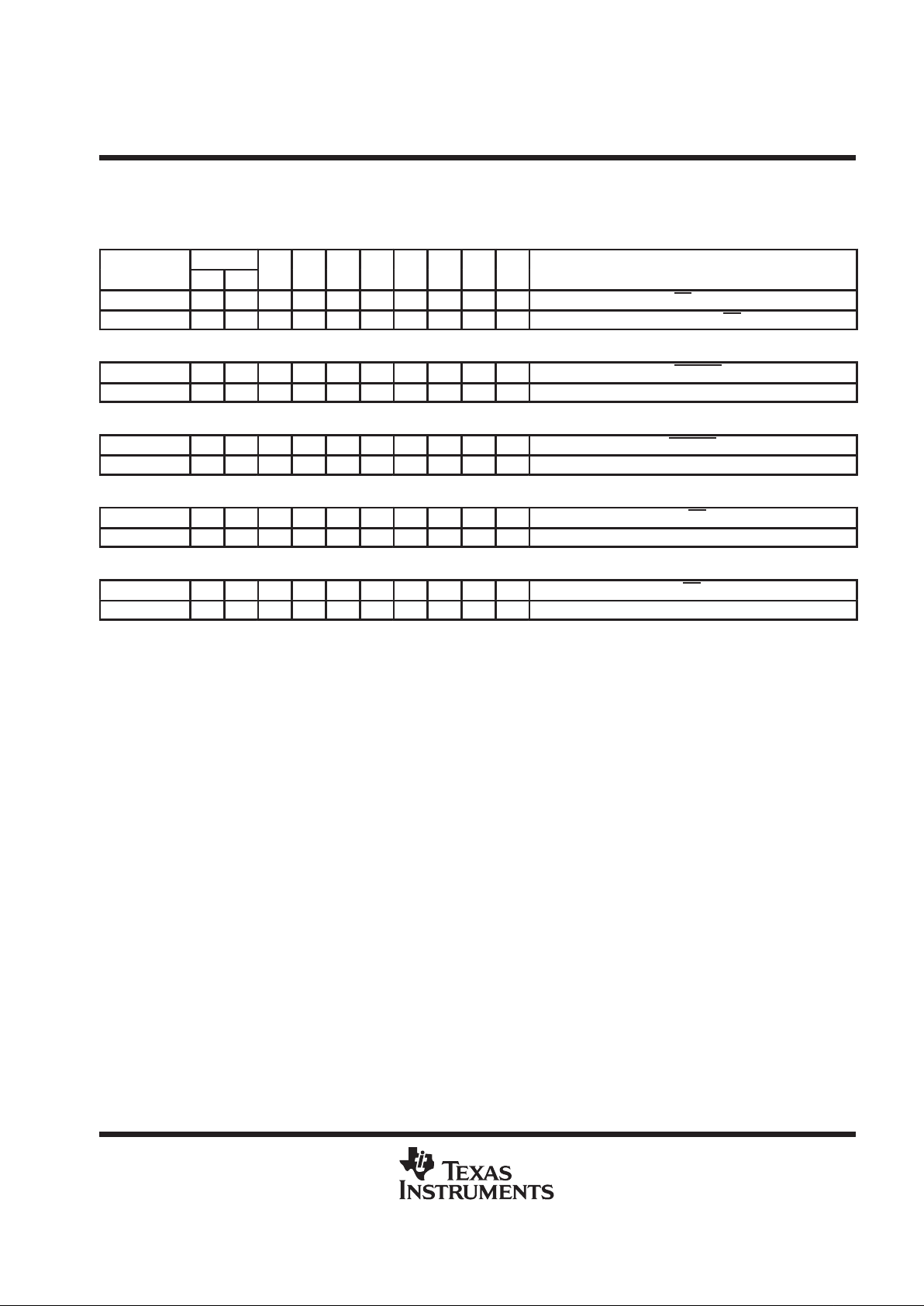
The following examples show how to program configuration registers CR0 and CR1 for different settings.
Example 1:
INDEX
REGISTER
D9 D8
D7 D6 D5 D4 D3 D2 D1 D0
COMMENT
CR0 0 0 1 1 0 1 0 0 0 0 Mono interrupt mode, use RD, write 0D0h to ADC
CR1 0 1 0 0 0 0 0 0 0 0 Use 2s complementary output, use RD, write 104h to ADC
Example 2:
CR0 0 0 1 1 0 1 0 0 0 0 Mono interrupt mode, use CSTART, write 0D0h to ADC
CR1 0 1 0 1 0 0 0 0 0 0 Use 2s complementary output, write 144h to ADC
Example 3:
CR0 0 0 1 1 0 1 0 1 0 0 Dual interrupt mode, use CSTART only, write 0D4h to ADC
CR1 0 1 0 1 0 0 0 0 0 0 Use 2s complementary output, write 144h to ADC
Example 4:
CR0 0 0 1 1 0 1 1 0 0 0 Mono continuous mode, use RD only, write 0D8h to ADC
CR1 0 1 0 0 0 0 0 0 0 0 Use 2s complementary output, write 104h to ADC
Example 5:
CRO 0 0 1 1 0 1 1 1 0 0 Dual continuous mode, use RD only, write 0DCh to ADC
CR1 0 1 0 0 0 0 0 1 0 0 Binary output, write 104h to ADC
analog input
input types
The four analog inputs can be configured as two pairs of differential inputs or four single-ended inputs by setting
the control register 0 bit 4 input type selection (dual or single channel).
differential input (CR0.4=1)
Up to two channels are available when the TL V1562 is programmed for differential input. The output data format
is bipolar when the device is operated in differential input mode.
single-ended input (CR0.4=0)
Up to four channels are available when the TLV1562 is programmed for single-ended input. The output data
format is unipolar when the device is operated in single-ended input mode.
TLV1562
2.7 V TO 5.5 V, HIGH-SPEED LOW-POWER RECONFIGURABLE ANALOG-TO-DIGITAL
CONVERTER WITH 4-INPUT, DUAL S/H, PARALLEL INTERFACE, AND POWER DOWN
SLAS162 – SEPTEMBER 1998
8
POST OFFICE BOX 655303 • DALLAS, TEXAS 75265
detailed description (continued)
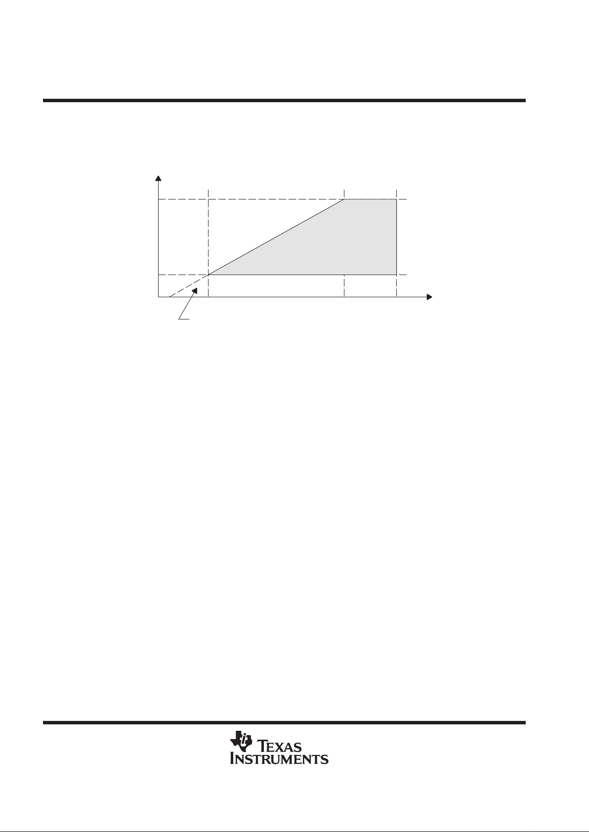
input signal range
The analog input signal range for a specific supply voltage AVDD ranges from (AVDD – 1.9 V) to 0.8 V.
3 V
0.8 V
2.7 4.9 5.5
AVDD (V)
V
SWING
Linearity not Guaranteed
Limited by Noise
Figure 3. Analog Input Range vs AV
DD
VREFCM + 0.5 × V
SWING
≤ AVDD –1 V
VREFCM – 0.5 × V
SWING
≥ 0.8 V
Where:
VREFCM = (VREFP + VREFM)/2 is the common mode reference voltage.
V
SWING
= dynamic range of the input signal,
V
SWING
= VINP – VINM,
And the common mode input voltage is:
VINCM = (VINP + VINM)/2,
MAX V
SWING
= MIN [(AVDD – 1.9 V), 3 V]
For single-ended input, the analog input range is between VREFP and VREFM. So the range of
single-ended VIN is:
3 V if AV
DD
= 3 V
1 V if AV
DD
= 3 V
0.8 V if AVDD = 2.7 V
For differential input, the input common mode voltage VINCM can be between A VDD and AGND as long as
3 V ≥ (VINP–VINM) ≥ 0.8 V.
This means VINCM ≥ 0.4 V.
So the range of differential analog input voltage, (VINP–VINM) is:
3 V if AV
DD
= 3 V
1 V if AVDD = 3 V
0.8 V if AVDD = 2.7 V
TLV1562
2.7 V TO 5.5 V, HIGH-SPEED LOW-POWER RECONFIGURABLE ANALOG-TO-DIGITAL
CONVERTER WITH 4-INPUT, DUAL S/H, PARALLEL INTERFACE, AND POWER DOWN
SLAS162 – SEPTEMBER 1998
9
POST OFFICE BOX 655303 • DALLAS, TEXAS 75265
detailed description (continued)
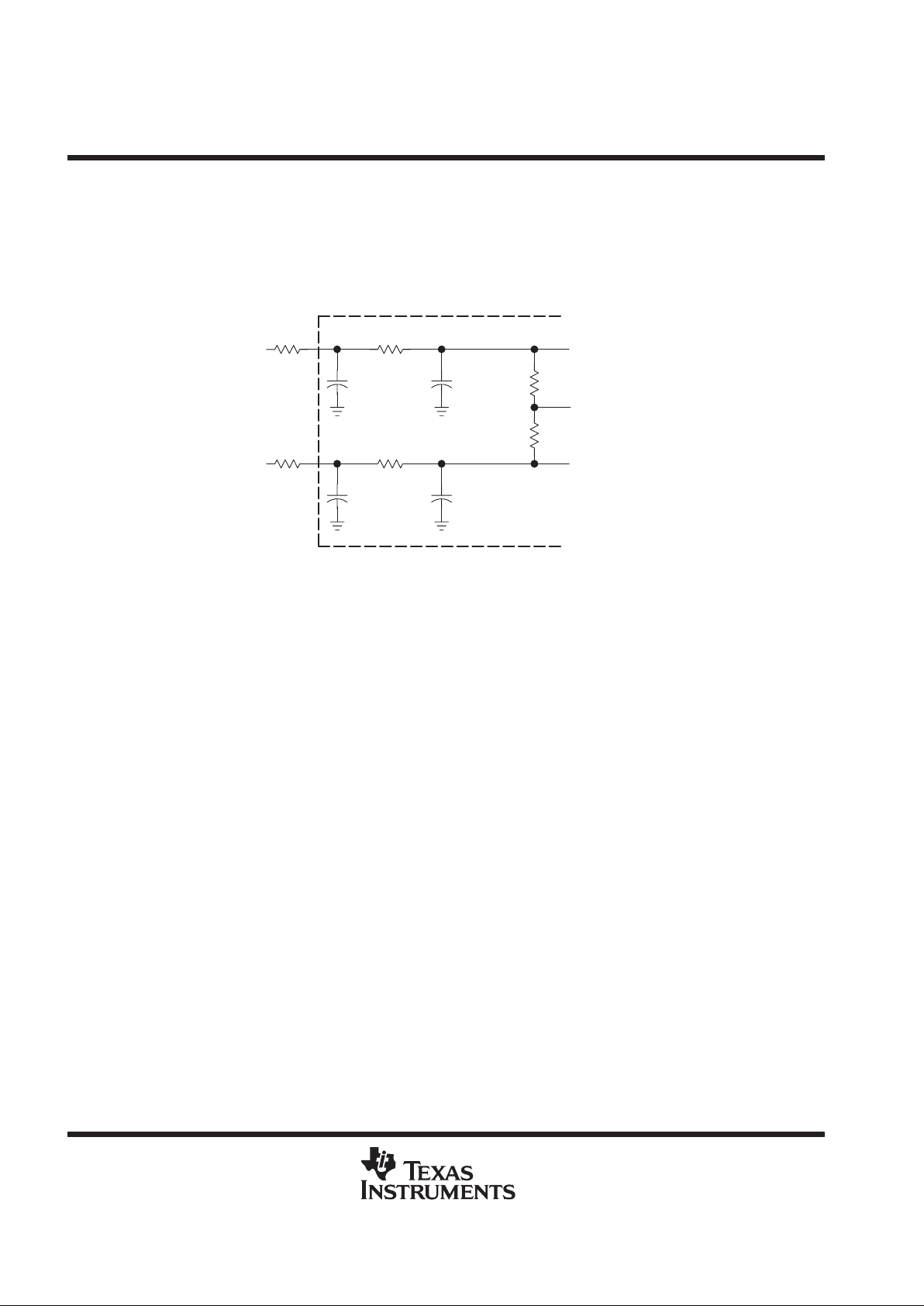
equivalent input impedance
VCC (V)
R
on(Ω)
1 k
0.5 k
2.7 5.5
V
in
C
pad
= 10 pF
0 V
C
sample
= 0.5 pF
FB
R
s
R
on
R
on
Buffer
Figure 4. Equivalent Input Circuit
Figure 5. Input Mux On Resistance vs
Analog Supply Voltage
Req = Vin/Ieq = (Q/Cin)/(Q/T) = T/Cin = 1/(fs × Csample) = 1/(2 MHz × 0.5 pF) = 1 MΩ
Where fs is the sampling frequency, and fc is the conversion frequency
f
s
= fc/5 when the device is in one channel/continuous conversion mode,
fs = fc/10 when the device is in one channel/continuous conversion mode,
f
s
= Conversion trigger strobe frequency when the device is in interrupt mode (RD or CSTART)
Csample = Input capacitance = 0.5 pF
Cparasitic = Parasitic capacitance = 0.5 pF
Cpad = Input PAD capacitance = 10 pF
Ron = Mux switch on series resistance = 1 kΩ at 2.7 V
Rs = Source output resistance = 1 kΩ
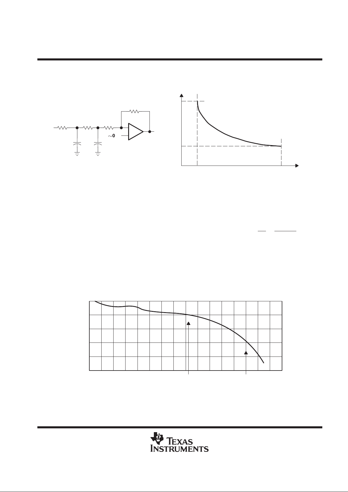
input bandwidth (full power 0 dB input, BW at –1 dB)
BW = 1/[2 × π × (Rtotal y Cac)]
= 1/[2 × π × ((Ron + Rs) × (Csample + Cparasitic))]
= 1/[2 × π × (2K × 1 pF)]
= 79.6 MHz (Theoretical Max)
–3
–4
–5
10
20 40
50
70 90 100
Attenuation in dB
–2
–1
Analog Input Frequency – MHz
0
120
130
15030
60 80
110
140
Figure 6. Typical Analog Input Frequency Input Bandwidth
TLV1562
2.7 V TO 5.5 V, HIGH-SPEED LOW-POWER RECONFIGURABLE ANALOG-TO-DIGITAL
CONVERTER WITH 4-INPUT, DUAL S/H, PARALLEL INTERFACE, AND POWER DOWN
SLAS162 – SEPTEMBER 1998
10
POST OFFICE BOX 655303 • DALLAS, TEXAS 75265
reference voltage inputs
The TL V1562 has two reference input pins: REFP and REFM. The voltage levels applied to these pins establish
the upper and lower limits of the analog inputs to produce a full-scale and zero-scale reading respectively . The
values of VREFP, VREFM, and the analog input should not exceed the positive supply or be less than GND
consistent with the specified absolute maximum ratings. The digital output is at full scale when the input signal
is equal to or higher than VREFP and is at zero when the input signal is equal to or lower than VREFM. The
internal resistance from VREFP to VREFM may be as low as 20 kΩ (±10%).
The reference voltages must satisfy the following conditions:
VREFP ≤ AVDD – 1 V,
AGND + 0.9 V < VREFM and
3 V ≥ (VREFP – VREFM) ≥ 0.8 V
V
REFP
C
pad
= 10 pF
Cin = 1 pF
V
REFM
C
pad
= 10 pF
Cin = 1 pF
10 kΩ
10 kΩ
VREFCM
R
on
R
on
R
s
R
s
Figure 7. Equivalent Circuit for Reference input
TLV1562
2.7 V TO 5.5 V, HIGH-SPEED LOW-POWER RECONFIGURABLE ANALOG-TO-DIGITAL
CONVERTER WITH 4-INPUT, DUAL S/H, PARALLEL INTERFACE, AND POWER DOWN
SLAS162 – SEPTEMBER 1998
11
POST OFFICE BOX 655303 • DALLAS, TEXAS 75265
sampling/conversion
All of the sampling, conversion, and data output in the device are started by a trigger. This trigger can be the
RD or CST ART signal depending on the mode of conversion and configuration. The falling edge of the RD signal
and the rising edge of the CST ART signal are extremely important since they are used to start the conversion.
These edges need to stay as close to the falling edges of the external clock, if they are used as SYSCLK. The
minimum setup time with respect to the rising edge of the external SYSCLK should be 5 ns minimum. When
the internal SYSCLK is used, this is not an issue, since these two edges start the internal clock automatically;
therefore, the setup time is always met.
USING EXTERNAL CLOCK
S/H Hold Time
t
s(TRGL-ECLKH)
Conversion Starts
Next Sampling Starts
t
d(ECLKL-TRGL)
Conversion Starts
Next Sampling Starts
Sampling Period
V
IH
V
IL
V
IH
V
IL
V
IH
V
IL
EXTERNAL
SYSCLK
RD
CSTART
Figure 8. Conversion Trigger Timing – External Clock
USING INTERNAL CLOCK
t
d(TRGL-ICLKH)
S/H Hold Time
Conversion Starts
Next Sampling
Starts
Conversion Starts Next Sampling Starts
V
IH
V
IL
V
IH
V
IL
V
IH
V
IL
RD
CSTART
INTERNAL
SYSCLK
INTERNAL
CLOCK STARTS
Figure 9. Conversion Trigger Timing – Internal Clock
TLV1562
2.7 V TO 5.5 V, HIGH-SPEED LOW-POWER RECONFIGURABLE ANALOG-TO-DIGITAL
CONVERTER WITH 4-INPUT, DUAL S/H, PARALLEL INTERFACE, AND POWER DOWN
SLAS162 – SEPTEMBER 1998
12
POST OFFICE BOX 655303 • DALLAS, TEXAS 75265
Table 2. Conversion Trigger Edge
CONVERSION
MODE
CONVERSION
TRIGGER
START OF
SAMPLING
START OF
CONVERSION
CONVERSION
TIME
(INTERNAL CLK)
CONVERSION
TIME
(EXTERNAL CLK)
INTERRUPT
CANCELED
BY
DATA OUT
Mono
Interrupt
RD WR ↑‡ or
2 SYSCLK from RD
↓
RD ↓ 6 SYSCLK 5 SYSCLK RD ↑ 41 ns§ from INT low
CSTAR T
†
CSTART ↓ CSTART ↑ 6 SYSCLK 5 SYSCLK RD ↓ 41 ns§ from RD low
Dual
Interrupt
CSTAR T CSTART ↓ CSTART ↑ 12 SYSCLK 10 SYSCLK First RD ↓ 41 ns§ from RD low
Mono
Continuous
RD WR ↑‡ or
2 SYSCLK from RD
↓
RD ↓ 6 SYSCLK 5 SYSCLK N/A 41 ns§ from RD low
Dual
Continuous
RD WR ↑‡ or
7 SYSCLK from RD
↓
RD ↓ 12 SYSCLK 10 SYSCLK N/A 41 ns§ from RD low
†
CSTART works with or without CS active.
‡
The first sampling period starts at the last RD
low of the previous cycle or WR high of the configuration cycle. RD low is the falling edge of RD
and WR high is the rising edge of the WR signal. (Minimum sample/hold amp settling time = one SYSCLK, approximately 100 ns min, at Rs ≤
1 kΩ).
§
Output data enable time is dependent on bus loading and supply voltage (BDVDD). For BDVDD = 5 V, the enable time is 19 ns at 25 pF, 23 ns
at 50 pF, and 25 ns at 100 pF. For BDVDD = 2.7 V , the enable time is 37 ns at 25 pF, 41 ns at 50 pF, and 56 ns at 100 pF.
The TLV1562 provides four types of conversion modes. The two interrupt-driven conversion modes are
asynchronous and are simple one-shot conversions. The auto-powerdown conversion feature can be enabled
when interrupt-driven conversion modes are used. The other two continuous conversion modes are
synchronous with the RD
signal (as a clock) from the processor and are more suitable for repetitive signal
measurement. These different modes of conversion offer a tradeoff between simplicity and speed.

TLV1562
2.7 V TO 5.5 V, HIGH-SPEED LOW-POWER RECONFIGURABLE ANALOG-TO-DIGITAL
CONVERTER WITH 4-INPUT, DUAL S/H, PARALLEL INTERFACE, AND POWER DOWN
SLAS162 – SEPTEMBER 1998
13
POST OFFICE BOX 655303 • DALLAS, TEXAS 75265
detailed description (continued)
Table 3. Maximum Conversion Speed (for 1 LSB INL and DNL at 10 bit)
MAXIMUM CONVERSION THROUGHPUT
†
CONVERSION MODE CR0.(3,2)
EXTERNAL CLOCK
(10 MHz)
INTERNAL CLOCK
(8 MHz)
RD 1.5 MSPS 1.1 MSPS
p
RD with auto power down
0.82 MSPS 0.68 MSPS
Mono interrupt-driven conversion mode
CSTART
00
1.5 MSPS 1.1 MSPS
CSTAR T with auto power down 0.82 MSPS 0.68 MSPS
p
CSTART
1.5 MSPS 0.91 MSPS
Dual interrupt-driven conversion mode
‡
CSTART with auto power down
01
1.05 MSPS 0.83 MSPS
Mono continuous conversion mode RD 10 2 MSPS
§
1.33 MSPS
§
Dual continuous conversion mode RD 11 2 MSPS
¶
1.33 MSPS
¶
†
Speed is calculated for 5-V with a 2-V reference
(5.5 V to 3 V , I-temperature and C-temperature: 2 MSPS at 10 bit, 3 MSPS at 8 bit, 7 MSPS at 4 bit;
3 V to 2.7 V , C-temperature: 2 MSPS at 10 bit, 2.5 MSPS at 8 bit, 7 MSPS at 4 bit;
3 V to 2.7 V , I-temperature: 1.6 MSPS at 10 bit, 2.5 MSPS at 8 bit, 7 MSPS at 4 bit).
Higher throughput is possible when the linearity requirement is relaxed.
‡
Dual interrupt mode is available to 8-bit or 10-bit resolution and single-ended input type.
§
Throughput from single selected channel.
¶
Combined throughputs from a pair of selected channels.
RD-Strobe
Mono Interrupt Mode: 0 RD-Delay
Mono Continuous Mode : 1 RD-Delay
Dual Continuous Mode : 2~3 RD
-Delay
Dual Interrupt Mode: 0~1 RD
-Delay
Conversion Results
Conversion Start
Figure 10. Digital Delays for Different Conversion Modes

TLV1562
2.7 V TO 5.5 V, HIGH-SPEED LOW-POWER RECONFIGURABLE ANALOG-TO-DIGITAL
CONVERTER WITH 4-INPUT, DUAL S/H, PARALLEL INTERFACE, AND POWER DOWN
SLAS162 – SEPTEMBER 1998
14
POST OFFICE BOX 655303 • DALLAS, TEXAS 75265
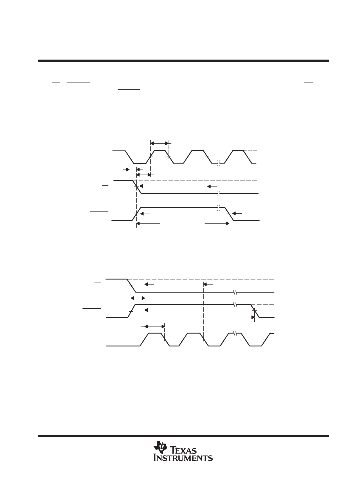
mono interrupt-driven mode (CR0.(3,2) = 0,0)
The mono interrupt-driven conversion mode provides a one-shot conversion. Sampling, conversion, and data
output are all performed in a single cycle. The analog signal is sampled 2 SYSCLKs after the falling edge of RD
(or the rising edge of WR if this is the first sample after configuration) and then converted on the falling edge
of RD. Once the data is ready, INT falls and the data is output to the bus. The rising edge of RD cancels INT
and initiates a read of the data. The data bus is 3-stated when RD goes high. It is not necessary to configure
the converter for each cycle or toggle CS between cycles.
V
IH
V
IL
V
IH
V
IL
V
IH
V
IL
V
IH
V
IL
V
IH
V
IL
t
s1
t
t
s1
t
conv1
t
d(RDL-SAMPLE)
t
d(RDL-CONV)
Hi–Z
t
en(DATAOUT)
t
d(CONV-INTL)
t
(APD)
t
dis(DATAOUT)
t
d(RDH-INTZ)
Power Down
(If Autopower Down is Set)
Power Down
(If Autopower Down is Set)
CS
CSTART
WR
RD
DATA
INT
conv1
Data 1
Sample 1 Conv 1 Sample 2 Conv 2
(With Pullup)
t
1(APDR)
t
1(APDR)
Figure 11. Mono Interrupt-Driven Mode Using RD

TLV1562
2.7 V TO 5.5 V, HIGH-SPEED LOW-POWER RECONFIGURABLE ANALOG-TO-DIGITAL
CONVERTER WITH 4-INPUT, DUAL S/H, PARALLEL INTERFACE, AND POWER DOWN
SLAS162 – SEPTEMBER 1998
15
POST OFFICE BOX 655303 • DALLAS, TEXAS 75265
Conversion can also be started with CSTART. This is useful when an application requires multiple TLV1562s
for simultaneous samplings and conversions. The falling edge of CSTART starts the sampling and the rising
edge of CST ART starts the conversion. Once the data is ready INT falls. INT is terminated by the following falling
edge of RD which also outputs the data to the bus. On the rising edge of RD, the data is read and the data bus
is 3-stated.
t
(APD)
Power Down
(If Autopower Down is Set)
Power Down
t
dis(DATAOUT)
t
d1(WRH–CSTARTL)
t
w(CSTARTL)
t
d(CSL-RDL)
t
d(RDH-CSTARTL)
t
s1
t
conv1
t
w(RDL)
t
s1
t
d(CSTART-SAMPLE)
t
d(INTL-CSL)
t
en(DATAOUT)
t
d(CSTARTL-SAMPLE)
t
d(RDH-INTZ)
t
d(CONV-INTL)
t
d1(CSTARTH–CONV)
V
IH
V
IL
CS
CSTART
WR
RD
DATA
INT
V
IH
V
IL
V
IH
V
IL
V
IH
V
IL
V
IH
V
IL
V
IH
V
IL
Data 1
(With Pullup)
Sample 1 Conv 1 Sample 2
t
1(APDR)
t
1(APDR)
Figure 12. Mono Interrupt-Driven Mode Using CSTART

TLV1562
2.7 V TO 5.5 V, HIGH-SPEED LOW-POWER RECONFIGURABLE ANALOG-TO-DIGITAL
CONVERTER WITH 4-INPUT, DUAL S/H, PARALLEL INTERFACE, AND POWER DOWN
SLAS162 – SEPTEMBER 1998
16
POST OFFICE BOX 655303 • DALLAS, TEXAS 75265
dual interrupt-driven mode (CR0.(3,2) = 0,1)
The dual interrupt-driven conversion mode provides a similar one-shot conversion, sampling, and conversion
but also samples both selected channels simultaneously. Conversion can only be started with the CSTART
signal. The falling edge of CSTART starts the sampling of both of the input channels selected, and the rising
edge of CSTART starts the conversion. Since it takes two consecutive conversions internally, the conversion
time required is doubled (10 SYSCLK cycles). Once the data are ready , INT falls. INT is terminated by the first
falling edge of RD, which also outputs the first data to the bus. On the rising edge of RD, data is read and the
data bus is 3-stated. The second RD falling edge outputs the second data to the bus and then reads it on the
rising edge and 3-states the bus. It is not necessary to configure the converter for each cycle or toggle CS
between cycles.
NOTE:Dual interrupt mode is available to 10-bit or 8-bit resolution and single-ended input
type.
t
EN(DATAOUT)
t
dis(DATAOUT)
t
2(APDR)
t
(APD)
Powerdown
(If Autopowerdown Is Set)
Powerdown
V
IH
V
IL
t
d2(WRH–CSTARTL)
t
d(INT-CSL)
t
w(CSH)
t
w(CSTARTL)
t
s4
t
conv2
t
w(RDL)
t
s4
t
en(DATAOUT)
t
d(RDL-INTZ)
t
2(APDR)
V
IH
V
IL
V
IH
V
IL
V
IH
V
IL
V
IH
V
IL
V
IH
V
IL
CS
CSTART
WR
RD
DATA
INT
Data 1A
Sample 1 Conv 1
Data 1B
Sample 2
t
d2(RDH–CSTARTL)
(With Pullup)
t
d2(CSTART–CONV)
t
dis(DATAOUT)
Figure 13. Dual Interrupt Conversion Mode
(Conversion can only be started with CSTART for the dual interrupt mode)

TLV1562
2.7 V TO 5.5 V, HIGH-SPEED LOW-POWER RECONFIGURABLE ANALOG-TO-DIGITAL
CONVERTER WITH 4-INPUT, DUAL S/H, PARALLEL INTERFACE, AND POWER DOWN
SLAS162 – SEPTEMBER 1998
17
POST OFFICE BOX 655303 • DALLAS, TEXAS 75265
mono continuous mode (CR0.(3,2) = 1,0)
The mono continuous mode of conversion is synchronous with the RD signal. Its cycle time is approximately
5 SYSCLK cycles when an external SYSCLK is used (6 SYSCLK cycles when an internal SYSCLK is used).
In the mono continuous mode, the TL V1562 is always sampling the input regardless of the state of other control
signals when it is not in the hold state (the first half SYSCLK cycle after each falling edge of RD
). This simplifies
control of the ADC. There is no need to generate any special signal to start the sampling.
V
IH
V
IL
V
IH
V
IL
V
IH
V
IL
V
IH
V
IL
t
c(RD)
t
conv1
t
(CONV1)
t
conv1
t
conv1
Hi-Z
CONV 1 CONV 2 CONV 3
t
s5
t
d(RDL-SAMPLE)
t
s2
t
s2
t
s2
Sample 1
Sample 2
Sample 3 Sample 4
Data 1 Data 2
t
en(DATAOUT)
t
dis(DATAOUT)
t
en(DATAOUT)
t
dis(DATAOUT)
Config
CS
WR
RD
DATA
t
w(RDL)
t
d(CSL-RDL)
Figure 14. Mono Continuous Mode

TLV1562
2.7 V TO 5.5 V, HIGH-SPEED LOW-POWER RECONFIGURABLE ANALOG-TO-DIGITAL
CONVERTER WITH 4-INPUT, DUAL S/H, PARALLEL INTERFACE, AND POWER DOWN
SLAS162 – SEPTEMBER 1998
18
POST OFFICE BOX 655303 • DALLAS, TEXAS 75265
dual continuous mode (CR0.(3,2) = 1,1)
When the TL V1562 operates in the dual continuous mode, it samples and then holds two preselected channels
(differential or single ended) simultaneously as RD clocks. These samples are then converted in sequence. This
is designed to optimize the DSP MIPS for communication applications. Its cycle time is approximately 10
SYSCLK cycles when an external SYSCLK is used (12 SYSCLK cycles when an internal SYSCLK is used).
When operating in the dual continuous mode, the TL V1562 is always sampling the input regardless of the state
of the other control signals when it is not in the hold state. This simplifies control of the ADC. There is no need
to generate any special signal to start the sampling. The TLV1562 goes into hold mode on the odd number
(starting from the rising edge of WR
) falling edge of RD for one SYSCLK clock cycle.
A two-depth FIFO is used (only in the dual continuous mode) to ensure the output correlation. Thus on every
alternate RD edge, the result of the previous two conversions is read out. This allows a slower RD clock
frequency (slower than 1/5 of the SYSCLK frequency). Each dual continuous mode cycle (while CS remains
active low) must have an even number of RD cycles to ensure the FIFO operates properly.
CS
WR
RD
DATA
t
dis(DATAOUT)
t
en(DATAOUT)
t
d(RDL-SAMPLE)
t
c(RD)
t
s5
t
conv2
t
conv2
t
conv2
CONV 1 CONV 2 CONV 3
t
s3
Sample 2
t
s3
Sample 3
t
s3
Sample 4
D 1A D 1B D 2AGFG
Sample 1
D 2B
V
IH
V
IL
Figure 15. Dual Continuous Mode
system clock source
The TL V1562 uses multiple clocks for dif ferent internal tasks. SYSCLK is used for most conversion subtasks.
The source of SYSCLK is programmable via control register 0, bit 5 (CR0.5). The source of SYSCLK is changed
at the rising edge of WR of the cycle when CR0.5 is programmed.
internal oscillator (CR0.5 = 0, SYSCLK = internal OSC)
The TL V1562 has a built-in 8-MHz oscillator . When the internal OSC is selected as the source of SYSCLK, the
internal clock starts with a delay (one half of the OSC clock period max) after the falling edge of the conversion
trigger (RD or CSTART).

TLV1562
2.7 V TO 5.5 V, HIGH-SPEED LOW-POWER RECONFIGURABLE ANALOG-TO-DIGITAL
CONVERTER WITH 4-INPUT, DUAL S/H, PARALLEL INTERFACE, AND POWER DOWN
SLAS162 – SEPTEMBER 1998
19
POST OFFICE BOX 655303 • DALLAS, TEXAS 75265
external clock input (CR0.5 = 1, SYSCLK = External Clk)
The TL V1562 is designed to operate with an external clock input (CMOS/TTL) with a frequency from 100 kHz
to 14 MHz. When an external clock is used as the source of SYSCLK, the setup time from the falling edge of
RD to the rising edge of SYSCLK, t
s(TRGL-ECLKH)
is 5 ns minimum. The internal OSC is shut down when the
external clock mode is selected.
host processor interface
parallel processor interface
The TL V1562 provides a generic high-speed parallel interface that is compatible with high-performance DSPs
and general-purpose microprocessors. These include D(0,9), RD, WR, and INT . RD transitions from high to low
to signal the end of acquisition. The parallel I/O has its own power supply to minimize digital noise.
output data format
The output data format is unipolar binary (1023 to 0) when the device is operated in the single-ended input mode
and is bipolar (51 1 to –512) when the device is operated in differential input mode. The output code format can
be either binary or 2s compliment. The output data format is controlled by CR1.2.
power down
The device offers two different power-down modes: Auto power-down mode for interrupt-driven conversions
and software power-down mode for all conversion modes. All configuration information is kept intact when the
device is in software or auto power-down mode.
auto-power down for interrupt-driven conversion modes
When auto-power down is enabled, the device turns off the analog section (the converter except for the
reference network) at the falling edge of INT and resumes after the falling edge of CS (if RD is the conversion
trigger) or CST ART (if CST ART is the conversion trigger). The reference current and I/O are kept alive to ensure
a fast recovery. Average power consumption can be reduced by accessing the converter less often. Special
requirements for using this feature are:
D
It is necessary to toggle CS between cycles so the converter knows when to resume.
D
There is an additional delay to a conversion after the device is accessed due to the auto-power-down
control. Therefore, the time between RD (or CST ART) triggers is longer (longer RD or CST AR T high time).
software power down (CR.10 = 1, software power down enabled)
In addition to the auto-power-down feature, the device has a software powerdown feature to further reduce
power consumption when the device is idle. Writing a 1 to control register bit CR1.0 puts the TLV1562 into
software power-down mode in 200 ns after CS is up. The device consumes less than 1 µA when in the
power-down mode. Writing a 0 to control register bit CR1.0 wakes up the device. Conversion can start 1 µs after
the device is resumed. CS must be high when the device is in power-down mode. Software power-down
operation is slower than auto-power down but is more flexible and consumes almost no power.

TLV1562
2.7 V TO 5.5 V, HIGH-SPEED LOW-POWER RECONFIGURABLE ANALOG-TO-DIGITAL
CONVERTER WITH 4-INPUT, DUAL S/H, PARALLEL INTERFACE, AND POWER DOWN
SLAS162 – SEPTEMBER 1998
20
POST OFFICE BOX 655303 • DALLAS, TEXAS 75265
T able 4. TLV1562 Powerdown Features
FUNCTION BLOCK/POWERDOWN MODE SOFTWARE POWERDOWN AUTO POWERDOWN
DIGITAL CONTROL VOLTAGE LEVEL CMOS TTL CMOS TTL
Converter analog section Inactive Inactive Inactive Inactive
Reference current (amps) Inactive Inactive Active Active
Digital I/O buffers Active active Active Active
Estimated supply current, I
CC
1 µA 80 µA 120 µA 200 µA
Power-down time 200 ns 200 ns 200 ns 200 ns
Resume time 1 µs 1 µs 700 ns 700 ns
Maximum throughput
†
1.2/0.7 MSPS‡1.2/0.7 MSPS
‡
1 MSPS 1 MSPS
†
Dual interrupt, 10-bit, 5-V AVDD, 10-MHz external clock, and 2 V (REFP–REFM).
‡
This assumes the TLV1562 is software powered down between every cycle. In reality this is not the case since auto-power down ma kes much
more sense in this case. So the realistic maximum throughput for software power down will be close to the maximum throughput without
powerdown which is 1.2 MSPS for dual-interrupt mode (and 1.5 MSPS if mono-interrupt mode is used). But this really depends on how long the
device is powered down.
mid-scale error calibration
The device has a ±5% maximum full-scale error, mid-scale error, and zero-scale error due to the gain error in
the sample and hold amplifier.
The TL V1562 is capable of calibrating the mid-scale error . There are two calibration modes: system mid-scale
error calibration and internal mid-scale error calibration as described below.
NOTE:
Set register CR0.(7,6) = 1,1 when the device is not in mid-scale error calibration mode.
These mid-scale error calibrations affect the ADCs transfer characteristics as shown in Figure 16. The absolute
error at code 512 is zero-out (this is the reference point for mid-scale error calibration). The calibration also
makes the FS error and ZS error equal.
internal mid-scale error calibration (CR0.(7,6) = 1,0)
The internal mid-scale error calibration mode is set by writing to the configuration registers with CR0.(7,6) set
to 10. The ADC analog inputs are internally shorted to mid-voltage (REFP+REFM)/2 when the mid-scale error
calibration mode is enabled. One conversion (initiated by the falling edge of RD) is performed to calculate the
offset. The result of this conversion is stored in the mid-scale error register and is subtracted from all subsequent
conversions thus removing any offset. Internal calibration removes any offsets internal to the device. Internal
mid-scale error calibration reduces the mid-scale error to ±2.5% FS single ended inputs (0.3% FS differential
inputs).
system mid-scale error calibration (CR0.(7,6) = 0,1)
System mid-scale error calibration is set by writing to the configuration registers with CR0.(7,6) set to 01. The
analog input to be calibrated is externally connected to the voltage corresponding to mid-code. For differential
operation, this is achieved by shorting the two inputs together; for a single-ended input this is achieved by
connecting the analog input to the system mid-voltage, (SYSTEM_REFP + SYSTEM_REFM)/2. One
conversion (initiated by RD
falling edge) is performed to calculate the offset. The result of this conversion is
stored in the mid-scale error register and is subtracted from all subsequent conversions thus removing any
offset. System mid-scale error calibration removes the offset of not only the ADC but any offsets in the entire
analog circuitry driving the ADC input. System mid-scale error calibration reduces the mid-scale error to ±0.4%
FS single ended inputs (0.25% FS differential inputs).

TLV1562
2.7 V TO 5.5 V, HIGH-SPEED LOW-POWER RECONFIGURABLE ANALOG-TO-DIGITAL
CONVERTER WITH 4-INPUT, DUAL S/H, PARALLEL INTERFACE, AND POWER DOWN
SLAS162 – SEPTEMBER 1998
21
POST OFFICE BOX 655303 • DALLAS, TEXAS 75265
Full-Scale Error
(Before Calibrayion)
Ideal Transfer Function
Transfer Function Before
Mid-Scale Calibration
Mid-Scale Error
(Before Calibration)
Mid-Scale Error
(After Calibration)
Analog Input
REFP
V-Mid (REFCM)
Zero-Scale Error
(Before Calibration)
Zero-Scale Error
(After Calibration)
Full-Scale Error
(After Calibration)
Transfer Function After
Mid-Scale Calibration
REFM
Zero Scale
Mid Scale
Full Scale
Code Output
Figure 16. Mid-Scale Error Calibration
resume normal conversion from mid-scale error calibration modes
A follow on write operation sets CR0.(7,6) to 00 which resumes the normal conversion mode. Typically
mid-scale error calibration needs to be performed only once after power up. If however the operation mode is
changed from single ended to differential, then preferably mid-scale error calibration should be performed
again.
The user writes a bit to enable mid-scale error calibration. Inputs to the ADC are internally shorted therefore
the offset value can be converted to a digital word. The result (a digital word representing the offset) is stored
in a latch. This offset value is then subtracted from the digital output of all conversions except when in mid-scale
error calibration mode.
system design consideration regarding to mid-scale error calibration
Mid-scale error calibration may limit the dynamic range of the ADC. If the offset is negative and has a magnitude
x, then the range of the converter codes is x to 1023. If the offset is positive and has a magnitude of x, then the
range of converter codes is 1 to 1023 –x. Thus the ADCs dynamic range is reduced by x (say x = 20 codes) on
either side of the range effectively with mid-scale error calibration. However this should not be a limitation for
most users.

TLV1562
2.7 V TO 5.5 V, HIGH-SPEED LOW-POWER RECONFIGURABLE ANALOG-TO-DIGITAL
CONVERTER WITH 4-INPUT, DUAL S/H, PARALLEL INTERFACE, AND POWER DOWN
SLAS162 – SEPTEMBER 1998
22
POST OFFICE BOX 655303 • DALLAS, TEXAS 75265
APPLICATION INFORMATION
2.7 V
10 kΩ
A15
A14
R/W
IS
DSPCLK
DSPINT
TMS320C541
Address Decoder
and Control
CS
WR
SYSCLK/5
RD
MODE
MUX
CSTART
INT
SYSCLK
10 kΩ 10 kΩ 10 kΩ
PD(0–9)
DVDDAV
DD
BDV
DD
RD
DGND AGND BDGND
SIG 1
SIG 2
REF
TLV1562
10
CS
WR
CSTART
INT
CLKIN
D(0–9)
CH1
CH3
Figure 17. Typical Interface to a TMS320 DSP

TLV1562
2.7 V TO 5.5 V, HIGH-SPEED LOW-POWER RECONFIGURABLE ANALOG-TO-DIGITAL
CONVERTER WITH 4-INPUT, DUAL S/H, PARALLEL INTERFACE, AND POWER DOWN
SLAS162 – SEPTEMBER 1998
23
POST OFFICE BOX 655303 • DALLAS, TEXAS 75265
APPLICATION INFORMATION
Set #3 in Single Interrupt Mode
Set #1 and #2 in Dual Interrupt Mode (New Mode)
Select (Separate RD Cycle option in Req Z for #1, #2, #3
C541
RD
WR
RD
WR
CSTART
CH0
CH2
Sig 1
Sig 2
1562 #1
INT 1
RD
WR
CSTART
CH0
CH2
Sig 3
Sig 4
#2
INT 2
RD
WR
CSTART
CH0
Sig 5#3
INT 3
CS
CS0
CS1
CS2
PD(0–9)
B I/O
(CSTART)
A
0
A
1
10
Figure 18. Multiple Chips Simultaneous Sampling/Conversion Application

TLV1562
2.7 V TO 5.5 V, HIGH-SPEED LOW-POWER RECONFIGURABLE ANALOG-TO-DIGITAL
CONVERTER WITH 4-INPUT, DUAL S/H, PARALLEL INTERFACE, AND POWER DOWN
SLAS162 – SEPTEMBER 1998
24
POST OFFICE BOX 655303 • DALLAS, TEXAS 75265
APPLICATION INFORMATION
Hi-Z
D Sig1 D Sig3 D Sig4 D Sig5
CS0
CS2
CS1
RD
PD(0–9)
CSTART
INT1
INT2
INT3
0.1 µs
< = 0.2 µs × 5
†
If CLK = 10 MHz
t
en(DATAOUT)
t
s4
t
conv2
V
IH
V
IL
V
IH
V
IL
V
IH
V
IL
V
IH
V
IL
V
IH
V
IL
V
IH
V
IL
V
IH
V
IL
V
IH
V
IL
V
IH
V
IL
D Sig2
t
dis(DATAOUT)
Pullup
Pullup
Pullup
Figure 19. Multiple Chips Simultaneous Sampling/Conversion Application System Timing

TLV1562
2.7 V TO 5.5 V, HIGH-SPEED LOW-POWER RECONFIGURABLE ANALOG-TO-DIGITAL
CONVERTER WITH 4-INPUT, DUAL S/H, PARALLEL INTERFACE, AND POWER DOWN
SLAS162 – SEPTEMBER 1998
25
POST OFFICE BOX 655303 • DALLAS, TEXAS 75265
absolute maximum ratings over operating free-air temperature range (unless otherwise noted)
†
Supply voltage range: AVDD (see Note 1) –0.5 V to 6.5 V. . . . . . . . . . . . . . . . . . . . . . . . . . . . . . . . . . . . . . . . . . . .
BDVDD, DVDD (see Note 2) –0.5 V to 6.5 V. . . . . . . . . . . . . . . . . . . . . . . . . . . . . . . . . . .
AVDD to DVDD or BDVDD –6.5 V to 6.5 V. . . . . . . . . . . . . . . . . . . . . . . . . . . . . . . . . . . . .
Voltage range between AGND and DGND or BDGND –0.3 V to 0.5 V. . . . . . . . . . . . . . . . . . . . . . . . . . . . . . . . .
Digital input voltage range, CLKIN, CS
, WR, RD, CSTART (see Note 2) –0.3 V to DVDD +0.3 V. . . . . . . . . . .
Digital data input voltage range (see Note 2) –0.3 V to DVDD +0.3 V. . . . . . . . . . . . . . . . . . . . . . . . . . . . . . . . . .
Digital data output voltage range (see Note 2) –0.3 V to DVDD +0.3 V. . . . . . . . . . . . . . . . . . . . . . . . . . . . . . . . .
Analog output voltage range, INT
(see Note 2) –0.1 V to AVDD+ 0.1 V. . . . . . . . . . . . . . . . . . . . . . . . . . . . . . . . .
Reference input voltage range, REFP (see Note 1) –0.1 V to AVDD+ 0.1 V. . . . . . . . . . . . . . . . . . . . . . . . . . . . .
Reference input voltage range, REFM (see Note 1) –0.3 V to 0.3 V. . . . . . . . . . . . . . . . . . . . . . . . . . . . . . . . . . .
Peak input current (any input) 20 mA. . . . . . . . . . . . . . . . . . . . . . . . . . . . . . . . . . . . . . . . . . . . . . . . . . . . . . . . . . . . .
Peak total input current (all inputs) –30 mA. . . . . . . . . . . . . . . . . . . . . . . . . . . . . . . . . . . . . . . . . . . . . . . . . . . . . . . .
Operating free-air temperature range, T
A
: TLV1562C –0°C to 70°C. . . . . . . . . . . . . . . . . . . . . . . . . . . . . . . . . . .
TLV1562I –40°C to 85°C. . . . . . . . . . . . . . . . . . . . . . . . . . . . . . . . . . .
Storage temperature range –65°C to 150°C. . . . . . . . . . . . . . . . . . . . . . . . . . . . . . . . . . . . . . . . . . . . . . . . . . . . . . . .
Lead temperature 1,6 mm (1/16 inch) from the case for 10 seconds 260°C. . . . . . . . . . . . . . . . . . . . . . . . . . . .
†
Stresses beyond those listed under “absolute maximum ratings” may cause permanent damage to the device. These are stress ratings only, and
functional operation of the device at these or any other conditions beyond those indicated under “recommended operating conditions” is not
implied. Exposure to absolute-maximum-rated conditions for extended periods may affect device reliability.
NOTES: 1. Measured with respect to AGND with REF – and GND wired together (unless otherwise noted).
2. Measured with respect to DGND.
recommended operating conditions
PARAMETERS MIN NOM MAX UNIT
Supply voltage, AVDD, BDVDD, DVDD (see Note 3) 2.7 5.5 V
Positive external reference voltage input, VREFP (see Note 4) AGND +1.7 AVDD – 1 V
Negative external reference voltage input, VREFM (see Note 4) AGND +0.9 AVDD – 1 V
Differential reference voltage input, (VREFP–VREFM) (see Note 4) 0.8
MIN of
AVDD – 1.9
or 3
V
Single-ended analog input voltage, (AIN – AGND) (see Note 4) VREFM VREFP V
Differential analog input voltage, (AINP–AINM) 0.8 3 V
Common mode analog input voltage, (AINP+AINM)/ 2 AGND AV
DD
V
External SYSCLK 40/60 cycle time, t
c(EXTSYSCLK)
0.067 1 µs
External SYSCLK pulse duraton high, t
wH(EXTSYSCLK)
40% 60%
tc(EXT
SYSCLK)
External SYSCLK pulse duration low, t
wL(EXTSYSCLK)
40% 60%
tc(EXT
SYSCLK)
High-level digital and control input voltage, V
IH
2.1 V
Low-level digital and control input voltage, V
IL
0.8 V
p
p
TLV1562C 0 70
°
Operating free-air temperature, T
A
TLV1562I –40 85
°C
NOTES: 3. The absolute difference between A VDD, BDVDD and DVDD should be less than 0.5 V .
4. Analog input voltages greater than that applied to VREFP convert as all ones (111111111111), while input voltages less than that
applied to VREFM convert as all zeros (000000000000).

TLV1562
2.7 V TO 5.5 V, HIGH-SPEED LOW-POWER RECONFIGURABLE ANALOG-TO-DIGITAL
CONVERTER WITH 4-INPUT, DUAL S/H, PARALLEL INTERFACE, AND POWER DOWN
SLAS162 – SEPTEMBER 1998
26
POST OFFICE BOX 655303 • DALLAS, TEXAS 75265
electrical characteristics over recommended operating free-air temperature range, differential
input, AV
DD
= DVDD =BDVDD = 3 V, VREFP – VREFM = 1 V, external SYSCLK = 10 MHz
(unless otherwise noted)
PARAMETER TEST CONDITIONS MIN TYP MAX UNIT
p
BDVDD = 5.5 V, IOH = –0.2 mA 2.4
VOHDigital high-level output voltage
BDVDD = 2.7 V, IOH = –20 µA BDVDD–0.1
V
p
BDVDD = 5.5 V, IOL = 0.8 mA 0.4
VOLDigital low-level output voltage
BDVDD = 2.7 V, IOL = 20 µA 0.1
V
Off-state output current
VO = BDVDD, CS = BDV
DD
0.005 1
I
OZ
(high-impedance state)
VO = BDGND,
CS = BDV
DD
–1 –0.005
µ
A
I
IH
High-level input current VI = BDV
DD
0.005 1 µA
I
IL
Low-level input current VI = BDGND –0.005 1 µA
Total operating supply current, (from
CS at BDGND, AVDD = 5.5 V,
SYSCLK = 10 MHz
8.5 11
gy ,(
AVDD, DVDD, and BDVDD)
CS at BDGND, AVDD = 2.7 V,
SYSCLK = 8 MHz
5 7
mA
Total auto-powerdown supply current
CS at BDGND, AVDD = 5.5 V,
SYSCLK = 10 MHz,
CMOS control level, Auto powerdown = 1
85 120
I
DD
y
(from AVDD, DVDD, and BDVDD)
CS at BDGND, AVDD = 5.5 V,
SYSCLK = 10 MHz,
TTL control level, Auto powerdown = 1
200 300
µ
A
Total S/W powerdown supply current
CS at BDGND, AVDD = 5.5 V,
SYSCLK = 10 MHz,
CMOS control level, S/W powerdown = 1
0.2 1
y
(from AVDD, DVDD, and BDVDD)
CS at BDGND, AVDD = 5.5 V,
SYSCLK = 10 MHz,
TTL control level, S/W powerdown = 1
60 80
µ
A
Selected channel at AV
DD
0.25 1
Selected channel leakage current
Selected channel at AGND 0.25 –1
µ
A
Maximum static analog reference
current into REFP
VREFP = AVDD – 1.9 V, AVDD = 5.5 V,
VREFM = AGND + 0.9 V, SYSCLK = 10 MHz
150 180 µA
Reference input impedance VDD = 5.5 V, CS = 0, SCLK = 10 MHz 17 25 30 kΩ
Output capacitance 5 pF
Analog inputs fixed 9 10
C
i
Input capacitance
Analog inputs switching
0.5 1
pF
Control inputs 20 25
p
VDD = 5.5 V 0.5
RONInput MUX ON resistance
VDD = 2.7 V 1
kΩ
†
All typical values are at VDD = 5 V, TA = 25°C.

TLV1562
2.7 V TO 5.5 V, HIGH-SPEED LOW-POWER RECONFIGURABLE ANALOG-TO-DIGITAL
CONVERTER WITH 4-INPUT, DUAL S/H, PARALLEL INTERFACE, AND POWER DOWN
SLAS162 – SEPTEMBER 1998
27
POST OFFICE BOX 655303 • DALLAS, TEXAS 75265
timing requirements
PARAMETER TEST CONDITIONS MIN TYP MAX UNIT
Delay time, CS↓ to WR↓, t
d(CSL–WRL)
2 4 ns
Delay time, RD↑ to CSTART↓, t
d1(RDH – CSTARTL)
100 ns
Delay time, RD↑ to CSTART↓, t
d2(RDH – CSTARTL)
300 ns
Delay time, WR↑ to CSTART↓, t
d1(WRH – CSTARTL)
100 ns
Delay time, WR↑ to CSTART↓, t
d2(WRH – CSTARTL)
300 ns
Delay time, CS↓ to RD↓, t
d(CSL–RDL)
2 4 ns
Pulse duration, CS high, t
w(CSH)
50 ns
Setup time, data valid to WR↑, t
su(DATAIN)
5 ns
Hold time, WR↑ to data invalid, t
h(DATAIN)
10 ns
Interrupt modes 50 ns
Pulse duration, RD lo
w,
t
w(RDL)
Continuous modes 200 ns
Pulse duration, WR low, t
w(WRL)
50 ns
Delay time, WR↑ to CS↑, t
d(WRH–CSH)
4 ns
Delay time, RD↑ to CS↑, t
d(RDH–CSH)
4 ns
Delay time, external SYSCLK↓ to RD↓, CSTART↑, t
d(ECLKL–TRGL)
0 2 ns
Setup time, RD↓, CSTART↑, to external SYSCLK↑, t
su(TRGL–ECLKH)
5 6 ns
Auto power down = 1 800
Pulse duration, CSTART lo
w,
t
w(CSTARTL)
Auto power down = 0 100
ns
Delay time, INT↓ to CS↓, t
d(INTL–CSL)
10 ns
External SYSCLK, 10 bit 5 5.5
Internal SYSCLK, 10 bit 6
p
External SYSCLK, 8 bit 4 4.5
Conversion time, mono continuous/interrupt mode, t
conv1
Internal SYSCLK, 8 bit 5
SYSCLK
External SYSCLK, 4 bit 2 2.5
Internal SYSCLK, 4 bit 3
External SYSCLK, 10 bit 10 11
Internal SYSCLK, 10 bit 12
p
External SYSCLK, 8 bit 8 9
Conversion time, dual continuous/interrupt mode, t
conv2
Internal SYSCLK, 8 bit 10
SYSCLK
External SYSCLK, 4 bit 4 5
Internal SYSCLK, 4 bit 6
External SYSCLK, 10 bit 5 5.5
Internal SYSCLK, 10 bit 6
External SYSCLK, 8 bit 4 4.5
Cycle time, continuous mode RD, t
c(RD)
Internal SYSCLK, 8 bit 5
SYSCLK
External SYSCLK, 4 bit 2 2.5
Internal SYSCLK, 4 bit 3
Mono interrupt mode sampling time or first cycle (mono interrupt or
continous mode) sampling time, t
s1
0.2 1000 µs
Dual interrupt mode sampling time or first cycle (dual interrupt or continuous
mode) sampling time, t
s4
0.3 1000 µs
Mono continuous mode sampling time, t
s2
3 SYSCLK
Dual continuous mode sampling time, t
s3
7 SYSCLK
Continuous mode first sampling time, t
(SAMPE5)
0.45 µs
Data rise time, t
r(DATAOUT)
3 5 10 ns

TLV1562
2.7 V TO 5.5 V, HIGH-SPEED LOW-POWER RECONFIGURABLE ANALOG-TO-DIGITAL
CONVERTER WITH 4-INPUT, DUAL S/H, PARALLEL INTERFACE, AND POWER DOWN
SLAS162 – SEPTEMBER 1998
28
POST OFFICE BOX 655303 • DALLAS, TEXAS 75265
timing requirements (continued)
PARAMETER TEST CONDITIONS MIN TYP MAX UNIT
Data fall time, t
f(DATAOUT)
2 4 8 ns
Control signal rise time, RD, RW, CSTART , CS, and DATA, t
r(I/O)
2 1000 ns
Control signal fall time, RD, RW, CSTART , CS, and DATA, t
f(I/O)
2 1000 ns
operating characteristics over recommended operating free-air temperature range (unless
otherwise noted)
PARAMETER TEST CONDITIONS MIN NOM MAX UNIT
fI = 800 kHz at 10 bit 2 MSPS, AVDD = 5 V, VREFP = 3.5 V
VREFM = 1.5 V , mono continuous
±0.6 ±1
fI = 800 kHz at 10 bit 2.5 MSPS, AVDD = 5 V , VREFP=3.5 V,
VREFM = 1.5 V, mono continuous
–1.5 ±0.85 ±1.5
fI = 800 kHz at 10 bit 2.8 MSPS, AVDD = 5 V,
VREFP = 3.5 V , VREFM = 1.5 V, mono continuous
±1.5
Integral linearity error, center best fit
fI = 800 kHz at 10 bit 2 MSPS, AVDD = 3 V, VREFP = 1.7 V,
VREFM = 0.9 V , mono continuous
±0.6 ±1
gy,
(see Note 5)
fI = 800 kHz at 8 bit 3 MSPS, AVDD = 3 V, VREFP = 1.7 V,
VREFM = 0.9 V , mono continuous
±0.6 ±1
LSB
fI = 800 kHz at 8 bit 3.5 MSPS, AVDD = 3 V, VREFP = 1.7 V,
VREFM = 0.9 V , mono continuous
±0.65 ±1
fI = 800 kHz at 8 bit 3.75 MSPS, AVDD = 5 V,
VREFP = 3.5 V , VREFM = 1.5 V, mono continuous
±1
fI = 800 kHz at 4 bit 7 MSPS, AVDD = 3 V, VREFP = 1.7 V,
VREFM = 0.9 V , mono continuous
±0.2 ±0.4
fI = 800 kHz at 10 bit 2 MSPS, AVDD = 5 V, VREFP = 3.5 V,
VREFM = 1.5 V , mono continuous
±0.5 ±1
fI = 800 kHz at 10 bit 2.5 MSPS, AVDD = 5 V,
VREFP = 3.5 V, VREFM = 1.5 V, mono continuous
–0.85 ±0.5 1.5
fI = 800 kHz at 10 bit 2.8 MSPS, AVDD = 5 V,
VREFP = 3.5 V , VREFM = 1.5 V, mono continuous
±0.9 1.5
fI = 800 kHz at 10 bit 2 MSPS, AVDD = 3 V, VREFP = 1.7 V,
VREFM = 0.9 V , mono continuous
±0.6 ±1
Differential linearity error
fI = 800 kHz at 8 bit 3 MSPS, AVDD = 3 V, VREFP = 1.7 V,
VREFM = 0.9 V , mono continuous
±0.5 ±1
LSB
fI = 800 kHz at 8 bit 3.5 MSPS, AVDD = 3 V, VREFP = 1.7 V,
VREFM = 0.9 V , mono continuous
–0.8 ±0.5 1
fI = 800 kHz at 8 bit 3.75 MSPS, AVDD = 5 V,
VREFP = 3.5 V , VREFM = 1.5 V, mono continuous
±1 1
fI = 800 kHz at 4 bit 7 MSPS, AVDD = 3 V, VREFP = 1.7 V,
VREFM = 0.9 V , mono continuous
±0.2 ±0.4
NOTE 5: Linear error is the maximum deviation from the best straight line through the A/D transfer characteristics.

TLV1562
2.7 V TO 5.5 V, HIGH-SPEED LOW-POWER RECONFIGURABLE ANALOG-TO-DIGITAL
CONVERTER WITH 4-INPUT, DUAL S/H, PARALLEL INTERFACE, AND POWER DOWN
SLAS162 – SEPTEMBER 1998
29
POST OFFICE BOX 655303 • DALLAS, TEXAS 75265
operating characteristics over recommended operating free-air temperature range (unless
otherwise noted) (continued)
PARAMETER TEST CONDITIONS MIN NOM MAX UNIT
Before calibration ±5
After system calibration, single-ended input ±0.4
Mid-scale error (see Note 6)
After system calibration, differential input ±0.25
%FS
After internal calibration, single-ended input ±2.5
After internal calibration, differential input ±0.3
Offset error (see Note 6) Before calibration ±5 %FS
Gain error (see Note 6) Before calibration ±5 %FS
Total unadjusted error (see Note 7) Before calibration ±5 %FS
Delay time, RD↓, CSTART↑ to external
SYSCLK↑, t
d(TRGL–ICLKH)
2ns 0.5 SYSCLK
Delay time, RD↓ to start of conversion
t
d(RDL–CONV1)
2 ns
Internal OSC frequency 7.5 MHz
Delay time, RD↑ to INT↑, t
d(RDH–INTZ)
1-kΩ pullup resistor, 10 pF, BDVDD = 5 V, use RD 10 ns
At 25 pF, BDVDD = 5 V 4
At 50 pF, BDVDD = 5 V 5
Disable time, RD↑ to data invalid,
At 100 pF, BDVDD = 5 V 7
, ,
t
dis(DATAOUT)
At 25 pF, BDVDD = 2.7 V 7
ns
At 50 pF, BDVDD = 2.7 V 10
At 100 pF, BDVDD = 2.7 V 14
At 25 pF, BDVDD = 5 V 20
At 50 pF, BDVDD = 5 V 25
Enable time, INT↓ to data valid,
At 100 pF, BDVDD = 5 V 30
, ,
t
en(DATAOUT)
At 25 pF, BDVDD = 2.7 V 37
ns
At 50 pF, BDVDD = 2.7 V 41
At 100 pF, BDVDD = 2.7 V 56
Delay time, mono interrupt mode pow-
Auto powerdown = 1 700
y,
er-up time, t
1(APDR)
Auto powerdown = 0 0
ns
Delay time, dual interrupt mode power-
Auto powerdown = 1 1000
y,
up time, t
2(APD)
Auto powerdown = 0 0
ns
p
Auto powerdown = 1 200
Delay time, INT↓ to powerdown, t
(APD)
Auto powerdown = 0 0
ns
Delay time, end of conversion to INT↓,
t
d(CONV-INTL)
5 10 ns
Delay time, RD↓ to INT Hi-Z,
t
d(RDL-INTZ)
1-kΩ pullup resistor, 10 pF, BDVDD = 5 V, Use CSTART 10 ns
Delay time, CSTAR T↑ to start of conversion 1, t
d1(CSTAR T H-CONV)
2 4 ns
Delay time, CSTAR T↑ to start of conversion 2, t
d2(CSTAR T H-CONV)
0.2 1000 µs
Delay time, RD↓ to sample,
t
d(RDL-SAMPLE)
2 SYSCLK
NOTES: 6. Zero error is the difference between 000000000000 and the converted output for zero input voltage: full-scale error is the difference
between 111111111111 and the converted output for full-scale input voltage
7. Total unadjusted error comprises linearity, zero, and full-scale errors

TLV1562
2.7 V TO 5.5 V, HIGH-SPEED LOW-POWER RECONFIGURABLE ANALOG-TO-DIGITAL
CONVERTER WITH 4-INPUT, DUAL S/H, PARALLEL INTERFACE, AND POWER DOWN
SLAS162 – SEPTEMBER 1998
30
POST OFFICE BOX 655303 • DALLAS, TEXAS 75265
operating characteristics over recommended operating free-air temperature range (unless
otherwise noted) (continued)
ac specifications
PARAMETER TEST CONDITIONS MIN TYP MAX UNIT
10-Bit Mode
fI = 800 kHz, at 10 bit 2 MSPS, AVDD = 5 V,
VREFP = 3.5 V , VREFM = 1.5 V, Mono continuous
8.97 9.4
ENOB
Effective number of bits
fI = 800 kHz, at 10 bit 1.6 MSPS, AVDD = 3 V,
VREFP = 1.7 V , VREFM = 0.9 V, Mono continuous
8.8 8.91
Bits
fI = 800 kHz, at 10 bit 2 MSPS, AVDD = 5 V,
VREFP = 3.5 V , VREFM = 1.5 V, Mono continuous
–68.8 –64.5
THD
Total harmonic distortion
fI = 800 kHz, at 10 bit 1.6 MSPS, AVDD = 3 V,
VREFP = 1.7 V , VREFM = 0.9 V, Mono continuous
–66.8 –64.5
dB
fI = 800 kHz, at 10 bit 2 MSPS, AVDD = 5 V,
VREFP = 3.5 V , VREFM = 1.5 V, Mono continuous
56.4 58.1
SNR
Signal-to-noise ratio
fI = 800 kHz, at 10 bit 1.6 MSPS, AVDD = 3 V,
VREFP = 1.7 V , VREFM = 0.9 V, Mono continuous
54.4 55.6
dB
fI = 800 kHz, at 10 bit 2 MSPS, AVDD = 5 V,
VREFP = 3.5 V , VREFM = 1.5 V, Mono continuous
56.2 57.8
SINAD
Signal-to-noise ratio +distortion
fI = 800 kHz, at 10 bit 1.6 MSPS, AVDD = 3 V,
VREFP = 1.7 V , VREFM = 0.9 V, Mono continuous
54.2 55.3
dB
p
fI = 800 kHz, at 10 bit 2 MSPS, AVDD = 5 V,
VREFP = 3.5 V , VREFM = 1.5 V, Mono continuous
–70.3 –67.5
SFDR
Spurious free dynamic range
fI = 800 kHz, at 10 bit 1.6 MSPS, AVDD = 3 V,
VREFP = 1.7 V , VREFM = 0.9 V, Mono continuous
–69.1 –66.5
dB
8-Bit Mode
ENOB Effective number of bits
fI = 800 kHz, at 8 bit 3 MSPS, AVDD = 3 V,
VREFP = 1.7 V , VREFM = 0.9 V, Mono continuous
7.93 Bits
THD Total harmonic distortion –64 dB
SNR Signal-to-noise ratio 49.2 dB
SINAD Signal-to-noise ratio +distortion 49 dB
SFDR Spurious free dynamic range –65 dB
4-Bit Mode
ENOB Effective number of bits
fI = 800 kHz, at 4 bit 7 MSPS, AVDD = 3 V,
VREFP = 1.7 V , VREFM = 0.9 V, Mono continuous
3.97 Bits
THD Total harmonic distortion –29 dB
SINAD Signal-to-noise ratio + distortion 26 dB
SINAD Signal-to-noise ratio + distortion 24 dB
SFDR Spurious free dynamic range –30.5 dB
Analog input
Cross talk rejection 68 dB
Full-power bandwidth, –3 dB 120 MHz
Full-power bandwidth, –1 dB 75 MHz

TLV1562
2.7 V TO 5.5 V, HIGH-SPEED LOW-POWER RECONFIGURABLE ANALOG-TO-DIGITAL
CONVERTER WITH 4-INPUT, DUAL S/H, PARALLEL INTERFACE, AND POWER DOWN
SLAS162 – SEPTEMBER 1998
31
POST OFFICE BOX 655303 • DALLAS, TEXAS 75265
TYPICAL CHARACTERISTICS
–0.5
–1
0511
INL – Integral Nonlinearity Error – LSB
0
0.5
Digital Output Code
1
1023
10-Bit Resolution,
VREF = 3.5 V–1.5 V ,
SYSCLK = 10 MHz
INTEGRAL NONLINEARITY ERROR
vs
DIGITAL OUTPUT CODE
Figure 20
–0.5
–1
0 127
0
0.5
1
255
INL – Integral Nonlinearity Error – LSB
Digital Output Code
8-Bit Resolution,
VREF = 4 V–1 V,
SYSCLK = 12 MHz
INTEGRAL NONLINEARITY ERROR
vs
DIGITAL OUTPUT CODE
Figure 21

TLV1562
2.7 V TO 5.5 V, HIGH-SPEED LOW-POWER RECONFIGURABLE ANALOG-TO-DIGITAL
CONVERTER WITH 4-INPUT, DUAL S/H, PARALLEL INTERFACE, AND POWER DOWN
SLAS162 – SEPTEMBER 1998
32
POST OFFICE BOX 655303 • DALLAS, TEXAS 75265
TYPICAL CHARACTERISTICS
–0.5
–1
07
INL – Integral Nonlinearity Error – LSB
0
0.5
Digital Output Code
1
15
4-Bit Resolution,
VREF = 4 V–1 V,
SYSCLK = 14 MHz
INTEGRAL NONLINEARITY ERROR
vs
DIGITAL OUTPUT CODE
Figure 22
–0.5
–1
0511
DNL – Differential Nonlinearity Error – LSB
0
0.5
Digital Output Code
1
1023
10-Bit Resolution, VREF = 3.5 V–1.5 V,
SYSCLK = 10 MHz
DIFFERENTIAL NONLINEARITY ERROR
vs
DIGITAL OUTPUT CODE
Figure 23

TLV1562
2.7 V TO 5.5 V, HIGH-SPEED LOW-POWER RECONFIGURABLE ANALOG-TO-DIGITAL
CONVERTER WITH 4-INPUT, DUAL S/H, PARALLEL INTERFACE, AND POWER DOWN
SLAS162 – SEPTEMBER 1998
33
POST OFFICE BOX 655303 • DALLAS, TEXAS 75265
TYPICAL CHARACTERISTICS
–0.5
–1
0 127
0
0.5
1
255
DNL – Differential Nonlinearity Error – LSB
Digital Output Code
8-Bit Resolution, VREF = 4 V–1 V ,
SYSCLK = 12 MHz
DIFFERENTIAL NONLINEARITY ERROR
vs
DIGITAL OUTPUT CODE
Figure 24
–1
07
0
0.5
1
–0.5
15
DNL – Differential Nonlinearity Error – LSB
Digital Output Code
8-Bit Resolution,
VREF = 4 V–1 V,
SYSCLK = 14 MHz
DIFFERENTIAL NONLINEARITY ERROR
vs
DIGITAL OUTPUT CODE
Figure 25

TLV1562
2.7 V TO 5.5 V, HIGH-SPEED LOW-POWER RECONFIGURABLE ANALOG-TO-DIGITAL
CONVERTER WITH 4-INPUT, DUAL S/H, PARALLEL INTERFACE, AND POWER DOWN
SLAS162 – SEPTEMBER 1998
34
POST OFFICE BOX 655303 • DALLAS, TEXAS 75265
TYPICAL CHARACTERISTICS
–0.5
–1
0511
INL – Integral Nonlinearity Error – LSB
0
Digital Output Code
1023
0.5
10-Bit Resolution, AVDD = 2.7 V,
VREF = 1.7 V–0.9 V , SYSCLK = 10 MHz
INTEGRAL NONLINEARITY ERROR
vs
DIGITAL OUTPUT CODE
1
Figure 26
–0.5
–1
0 127
0
0.5
1
255
DNL – Differential Nonlinearity Error – LSB
Digital Output Code
8-Bit Resolution, AVDD = 3 V,
VREF = 1.7 V–0.9 V , SYSCLK = 10 MHz
DIFFERENTIAL NONLINEARITY ERROR
vs
DIGITAL OUTPUT CODE
Figure 27

TLV1562
2.7 V TO 5.5 V, HIGH-SPEED LOW-POWER RECONFIGURABLE ANALOG-TO-DIGITAL
CONVERTER WITH 4-INPUT, DUAL S/H, PARALLEL INTERFACE, AND POWER DOWN
SLAS162 – SEPTEMBER 1998
35
POST OFFICE BOX 655303 • DALLAS, TEXAS 75265
TYPICAL CHARACTERISTICS
–1
07
0
0.5
1
–0.5
15
DNL – Differential Nonlinearity Error – LSB
Digital Output Code
8-Bit Resolution, AVDD = 2.7 V,
VREF = 1.7 V–0.9 V , SYSCLK = 14 MHz
DIFFERENTIAL NONLINEARITY ERROR
vs
DIGITAL OUTPUT CODE
Figure 28
–0.5
–1
0511
0
0.5
1
1023
DNL – Differential Nonlinearity Error – LSB
Digital Output Code
10-Bit Resolution, AVDD = 2.7 V, VREFP = 1.7 V,
VREFM = 0.9 V , Internal Clock
DIFFERENTIAL NONLINEARITY ERROR
vs
DIGITAL OUTPUT CODE
Figure 29

TLV1562
2.7 V TO 5.5 V, HIGH-SPEED LOW-POWER RECONFIGURABLE ANALOG-TO-DIGITAL
CONVERTER WITH 4-INPUT, DUAL S/H, PARALLEL INTERFACE, AND POWER DOWN
SLAS162 – SEPTEMBER 1998
36
POST OFFICE BOX 655303 • DALLAS, TEXAS 75265
TYPICAL CHARACTERISTICS
–0.6
–1
0 127
0
0.8
1
255
0.6
0.4
0.2
–0.2
–0.4
–0.8
DNL – Differential Nonlinearity Error – LSB
Digital Output Code
8-Bit Resolution, AVDD = 2.7 V, REFP = 1.7 V, REFM = 0.9 V, 12 MHz
External Clock
DIFFERENTIAL NONLINEARITY ERROR
vs
DIGITAL OUTPUT CODE
Figure 30
–0.6
–1
07
DNL – Differential Nonlinearity Error – LSB
0
0.4
Digital Output Code
1
15
0.8
0.6
0.2
–0.2
–0.4
–0.8
4-Bit Resolution, AVDD = 2.7 V, REFP = 1.7 V, REFM = 0.9 V, 14 MHz
External Clock
DIFFERENTIAL NONLINEARITY ERROR
vs
DIGITAL OUTPUT CODE
Figure 31

TLV1562
2.7 V TO 5.5 V, HIGH-SPEED LOW-POWER RECONFIGURABLE ANALOG-TO-DIGITAL
CONVERTER WITH 4-INPUT, DUAL S/H, PARALLEL INTERFACE, AND POWER DOWN
SLAS162 – SEPTEMBER 1998
37
POST OFFICE BOX 655303 • DALLAS, TEXAS 75265
TYPICAL CHARACTERISTICS
Figure 32
8
6
2
0
0 2 4 7 10 12 15
Typical Supply Current – mA
10
14
f – Clock Frequency – MHz
TYPICAL SUPPLY CURRENT
vs
FREQUENCY
16
20
AVDD = 5.5 V
AVDD = 2.7 V
12
4
Figure 33
40
20
0
Total Current –
60
80
TYPICAL POWER DOWN CURRENT
vs
TEMPERATURE
100
Aµ
T – Temperature –°C
AVDD = 5.5 V at 90°C
AVDD = 5.5 V at 25°C
AVDD = 5.5 V at 40°C
AVDD = 3 V at 40°C
Figure 34
–70.5
–71
–72
–72.5
50 100 200 300 400 500 600
SFDR – Magnitude – dB
–70
–69
Analog Input Frequency – kHz
SPURIOUS FREE DYNAMIC RANGE
vs
INPUT FREQUENCY
–68.5
700 800 900 1000
–69.5
–71.5
AVDD = 3 V, VREF+ = 2 V, VREF = 1 V
AVDD = 5 V, VREF+ = 3.5 V, VREF = 1.5 V
AVDD = 5 V, VREF+ = 4 V, VREF = 1.5 V
Figure 35
57
56
54
53
50 100 200 300 400 500 600
SNR – Magnitude – dB
59
60
Analog Input Frequency – kHz
SIGNAL TO NOISE
vs
INPUT FREQUENCY
61
700 800 9001000
58
55
AVDD = 5 V, VREF+ = 4 V, VREF = 1 V
AVDD = 5 V, VREF+ = 3.5 V, VREF = 1.5 V
AVDD = 3 V, VREF+ = 2 V, VREF = 1 V

TLV1562
2.7 V TO 5.5 V, HIGH-SPEED LOW-POWER RECONFIGURABLE ANALOG-TO-DIGITAL
CONVERTER WITH 4-INPUT, DUAL S/H, PARALLEL INTERFACE, AND POWER DOWN
SLAS162 – SEPTEMBER 1998
38
POST OFFICE BOX 655303 • DALLAS, TEXAS 75265
TYPICAL CHARACTERISTICS
Figure 36
AVDD = 3 V, VREF+ = 2 V, VREF = 1 V
57
56
54
53
50 100 200 300 400 500 600
SINAD – Magnitude – dB
59
60
Analog Input Frequency – kHz
SIGNAL TO NOISE HARMONIC DISTORTION
vs
INPUT FREQUENCY
61
700 800 900 1000
58
55
AVDD = 5 V, VREF+ = 4 V, VREF = 1 V
AVDD = 5 V, VREF+ = 3.5 V, VREF = 1.5 V
Figure 37
9
8.8
8.6
8.4
50 100 200 300 400 500 600
Effective Number of Bits
9.4
9.6
Analog Input Frequency – kHz
EFFECTIVE NUMBER OF BITS
vs
INPUT FREQUENCY
9.8
700 800 900 1000
9.2
AVDD = 5 V, VREF+ = 3.5 V, VREF = 1.5 V
AVDD = 5 V, VREF+ = 4 V, VREF = 1 V
AVDD = 3 V, VREF+ = 2 V, VREF = 1 V
AVDD = 5 V, VREF+ = 3.5 V, VREF = 1.5 V
–69
–69.5
–70
–70.5
50 100 200 300 400 500 600
THD – Magnitude – dB
–68
–67.5
Analog Input Frequency – kHz
TOTAL HARMONIC DISTORTION
vs
INPUT FREQUENCY
–67
700 800 900 1000
–68.5
AVDD = 3 V, VREF+ = 2 V, VREF = 1 V
AVDD = 5 V, VREF+ = 4 V, VREF = 1 V
Figure 38

TLV1562
2.7 V TO 5.5 V, HIGH-SPEED LOW-POWER RECONFIGURABLE ANALOG-TO-DIGITAL
CONVERTER WITH 4-INPUT, DUAL S/H, PARALLEL INTERFACE, AND POWER DOWN
SLAS162 – SEPTEMBER 1998
39
POST OFFICE BOX 655303 • DALLAS, TEXAS 75265
APPLICATION INFORMATION
1000000000
0111111111
0000000010
0000000001
0000000000
1111111110
0 0.0096 2.4528 2.4576 2.4624
Digital Output Code
1000000001
1111111101
1111111111
4.9056 4.9104 4.9152
512
511
2
1
0
1022
Step
513
1021
1023
0.0024
VI – Analog Input Voltage – V
VZT = VZS + 1/2 LSB
V
ZS
See Notes A and B
4.9080
0.0048
VFT = VFS – 1/2 LSB
V
FS
NOTES: A. This curve is based on the assumption that V
ref+
and V
ref–
have been adjusted so that the voltage at the transition from digital 0
to 1 (VZT) is 0.0024 V and the transition to full scale (VFT) is 4.908 V . 1 LSB = 4.8 mV.
B. The full-scale value (VFS) is the step whose nominal midstep value has the highest absolute value. The zero-scale value (VZS) is
the step whose nominal midstep value equals zero.
Figure 39. Ideal 12-Bit ADC Conversion Characteristics

IMPORTANT NOTICE
T exas Instruments and its subsidiaries (TI) reserve the right to make changes to their products or to discontinue
any product or service without notice, and advise customers to obtain the latest version of relevant information
to verify, before placing orders, that information being relied on is current and complete. All products are sold
subject to the terms and conditions of sale supplied at the time of order acknowledgement, including those
pertaining to warranty, patent infringement, and limitation of liability.
TI warrants performance of its semiconductor products to the specifications applicable at the time of sale in
accordance with TI’s standard warranty. Testing and other quality control techniques are utilized to the extent
TI deems necessary to support this warranty. Specific testing of all parameters of each device is not necessarily
performed, except those mandated by government requirements.
CERT AIN APPLICATIONS USING SEMICONDUCTOR PRODUCTS MAY INVOLVE POTENTIAL RISKS OF
DEATH, PERSONAL INJURY, OR SEVERE PROPERTY OR ENVIRONMENTAL DAMAGE (“CRITICAL
APPLICATIONS”). TI SEMICONDUCTOR PRODUCTS ARE NOT DESIGNED, AUTHORIZED, OR
WARRANTED TO BE SUITABLE FOR USE IN LIFE-SUPPORT DEVICES OR SYSTEMS OR OTHER
CRITICAL APPLICATIONS. INCLUSION OF TI PRODUCTS IN SUCH APPLICA TIONS IS UNDERSTOOD T O
BE FULLY AT THE CUSTOMER’S RISK.
In order to minimize risks associated with the customer’s applications, adequate design and operating
safeguards must be provided by the customer to minimize inherent or procedural hazards.
TI assumes no liability for applications assistance or customer product design. TI does not warrant or represent
that any license, either express or implied, is granted under any patent right, copyright, mask work right, or other
intellectual property right of TI covering or relating to any combination, machine, or process in which such
semiconductor products or services might be or are used. TI’s publication of information regarding any third
party’s products or services does not constitute TI’s approval, warranty or endorsement thereof.
Copyright 1999, Texas Instruments Incorporated
 Loading...