

T
SYMBOL
TLV1391
SINGLE DIFFERENTIAL COMPARATORS
SLCS128B – APRIL 1996 – REVISED JUNE 1999
D
Low-Voltage and Single-Supply Operation
V
= 2 V to 7 V
CC
D
Common-Mode Voltage Range Includes
Ground
D
Fast Response Time . . . 0.7 µs Typ
D
Low Supply Current ...80 µA Typ and
150 µA Max
D
Fully Specified at 3-V and 5-V Supply
V
/GND
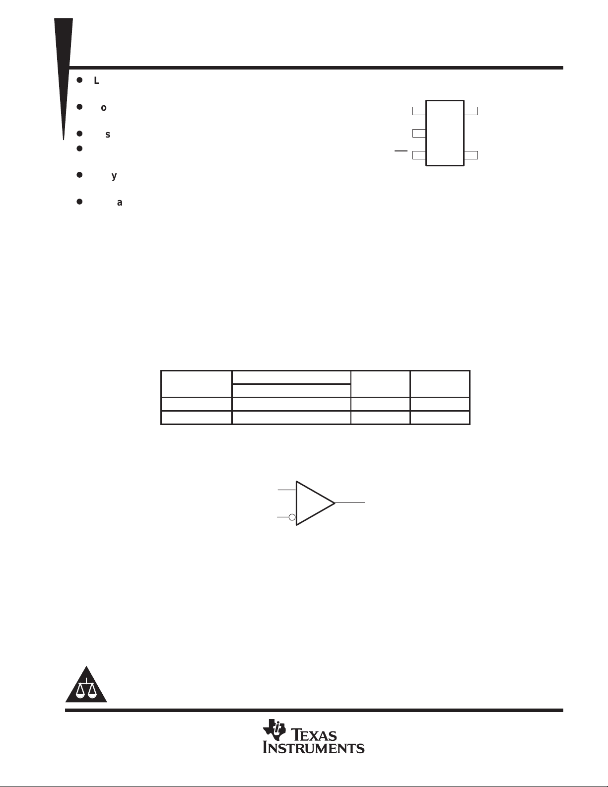
DBV PACKAGE
IN–
CC–
IN+
(TOP VIEW)
1
5
2
3
4
V
CC+
OUT
Voltages
D
Available in SOT-23 (DBV) Packaging
description
The TLV1391 is a differential comparator built using a Texas Instruments low-voltage, high-speed bipolar
process. These devices have been developed specifically for low-voltage, single-supply applications. Their
enhanced performance makes them excellent replacements for the LM393 in the improved 3-V and 5-V system
designs of today.
The TL V1391, with its typical supply current of only 80 µA, is ideal for low-power systems. Response time also
has been improved to 0.7 µs.
The TL V1391C is characterized for operation from 0°C to 70°C and the TL V1391I is characterized for operation
from –40°C to 85°C.
AVAILABLE OPTIONS
A
0°C to 70°C TLV1391CDBV VABC TLV1391Y
–40°C to 85°C TLV1391IDBV VABI
†
The DBV package is only available taped and reeled. Chip forms are specified for
operation at 25°C only.
PACKAGED DEVICES
SOT-23 (DBV)
CHIP FORM
(Y)
symbol (each comparator)
Please be aware that an important notice concerning availability, standard warranty, and use in critical applications of
Texas Instruments semiconductor products and disclaimers thereto appears at the end of this data sheet.
PRODUCTION DATA information is current as of publication date.
Products conform to specifications per the terms of Texas Instruments
standard warranty. Production processing does not necessarily include
testing of all parameters.
IN+
OUT
IN–
Copyright 1999, Texas Instruments Incorporated
POST OFFICE BOX 655303 • DALLAS, TEXAS 75265
1
TLV1391
SINGLE DIFFERENTIAL COMPARATORS
SLCS128B – APRIL 1996 – REVISED JUNE 1999
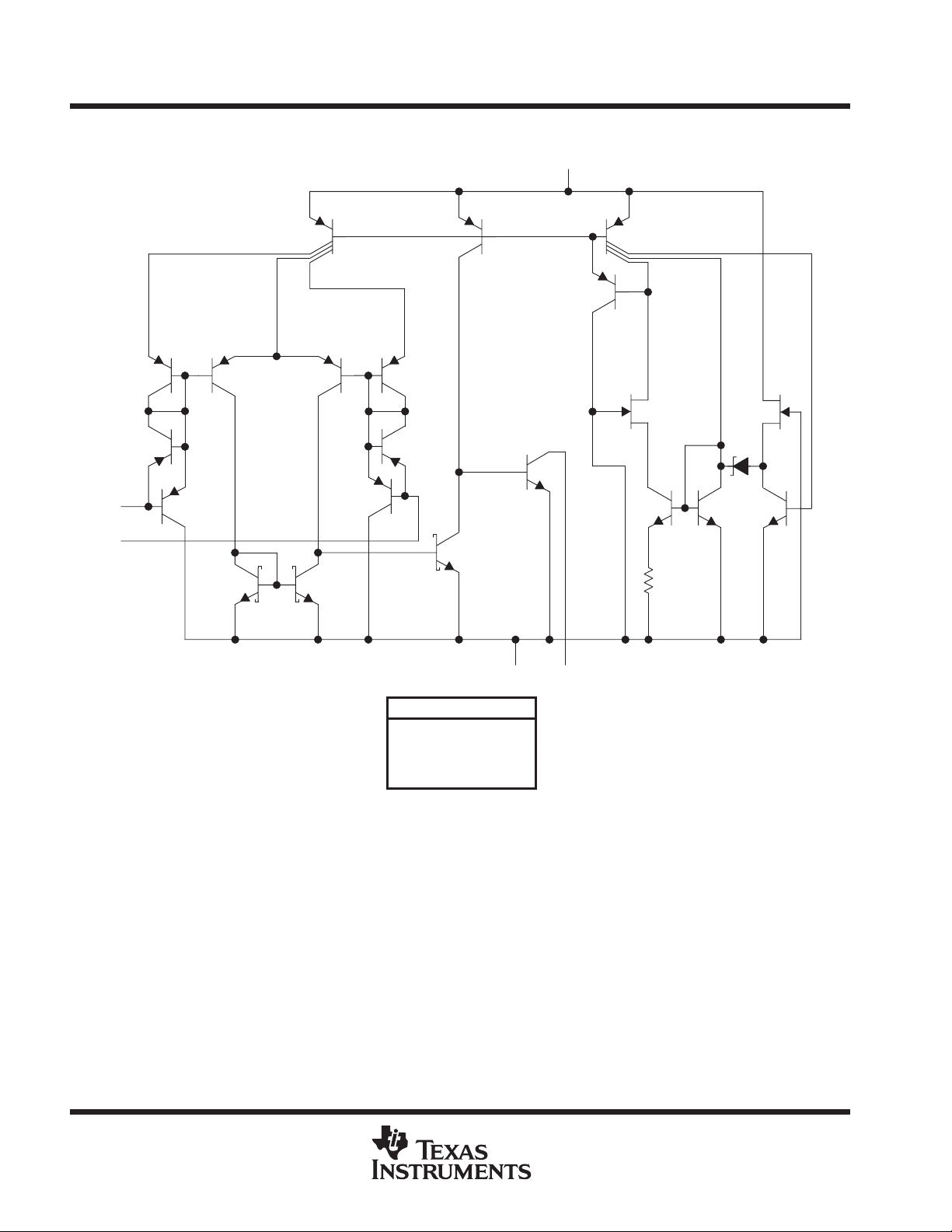
TLV1391, TLV1391Y equivalent schematic
V
CC
IN +
IN –
GND OUT
COMPONENT COUNT
Transistors 26
Resistors 1
Diodes
Epi-FET 1
4
2
POST OFFICE BOX 655303 • DALLAS, TEXAS 75265
O erating free-air tem erature, T
A
°C
TLV1391
SINGLE DIFFERENTIAL COMPARATORS
SLCS128B – APRIL 1996 – REVISED JUNE 1999
absolute maximum ratings over operating free-air temperature range (unless otherwise noted)
Supply voltage, V
Differential input voltage, V
Input voltage, V
Output voltage, V
Output current, I
Duration of short-circuit current to GND (see Note 3) Unlimited. . . . . . . . . . . . . . . . . . . . . . . . . . . . . . . . . . . . . . .
Package thermal impedance, θ
Lead temperature 1,6 mm (1/16 inch) from case for 10 seconds 260°C. . . . . . . . . . . . . . . . . . . . . . . . . . . . . . .
Storage temperature range, T
†
Stresses beyond those listed under “absolute maximum ratings” may cause permanent damage to the device. These are stress ratings only, and
functional operation of the device at these or any other conditions beyond those indicated under “recommended operating conditions” is not
implied. Exposure to absolute-maximum-rated conditions for extended periods may affect device reliability.
NOTES: 1. All voltage values, except differential voltages, are with respect to the network GND.
2. Differential voltages are at the noninverting input with respect to the inverting input.
3. Short circuits from the outputs to VCC can cause excessive heating and eventual destruction of the chip.
4. Maximum power dissipation is a function of TJ(max),
ambient temperature is PD = (TJ(max) – TA)/
5. The package thermal impedance is calculated in accordance with JESD 51.
(see Note 1) 7 V. . . . . . . . . . . . . . . . . . . . . . . . . . . . . . . . . . . . . . . . . . . . . . . . . . . . . . . . . . . . .
CC
(any input) –0.3 V to V
I
7 V. . . . . . . . . . . . . . . . . . . . . . . . . . . . . . . . . . . . . . . . . . . . . . . . . . . . . . . . . . . . . . . . . . . . . . . . . .
O
(each output) 20 mA. . . . . . . . . . . . . . . . . . . . . . . . . . . . . . . . . . . . . . . . . . . . . . . . . . . . . . . . . . .
O
(see Note 2) ±7 V. . . . . . . . . . . . . . . . . . . . . . . . . . . . . . . . . . . . . . . . . . . . . . . . . . . .
ID
. . . . . . . . . . . . . . . . . . . . . . . . . . . . . . . . . . . . . . . . . . . . . . . . . . . . . . . .
(see Note 4 and 5) 347°C/W. . . . . . . . . . . . . . . . . . . . . . . . . . . . . . . . . . . . . . .
JA
–65°C to 150°C. . . . . . . . . . . . . . . . . . . . . . . . . . . . . . . . . . . . . . . . . . . . . . . . . . .
stg
θ
, and TA. The maximum allowable power dissipation at any allowable
θ
JA
JA
. Operating at the absolute maximum TJ of 150°C can impact reliability.
recommended operating conditions
Supply voltage, V
p
CC
MIN MAX
2 7 V
p
TLV1391C 0 70
TLV1391I –40 85
UNIT
°
†
CC
POST OFFICE BOX 655303 • DALLAS, TEXAS 75265
3

TLV1391
PARAMETER
TEST CONDITIONS
T
†
UNIT
VIOInput offset voltage
V
V
V
(min)
mV
V
Common-mode input voltage range
V
IIOInput offset current
V
V
nA
IIBInput bias current
V
V
nA
IOHHigh-level output current
nA
I
High-level supply current
V
V
A
I
Low-level supply current
V
V
A
PARAMETER
TEST CONDITIONS
UNIT
SINGLE DIFFERENTIAL COMPARATORS
SLCS128B – APRIL 1996 – REVISED JUNE 1999
electrical characteristics, VCC = 3 V
p
ICR
V
OL
I
OL
CC(H)
CC(L)
†
Full range is 0°C to 70°C.
Low-level output voltage VID = –1 V, IOL = 500 µA Full range 120 300 mV
p
p
Low-level output current VID = –1 V, VOL = 1.5 V 25°C 500 µA
p
p
pp
pp
= 1.4 V,
O
= 1.4
O
= 1.4
O
VID = 1 V, VOH = 3 V 25°C 0.1
VID = 1 V, VOH = 5 V Full range 100
=
O
OH
=
O
OL
A
=
IC
ICR
25°C 1.5 5
Full range 9
25°C
Full range
25°C 5 50
Full range 150
25°C –40 –250
Full range –400
25°C 80 125
Full range 150
25°C 80 125
Full range 150
VCC – 1.5
VCC –2
TLV1391C
MIN TYP MAX
0 to
0 to
0 to
VCC –1.2
µ
µ
switching characteristics, VCC = 3 V, CL = 15 pF‡, T
Response time
‡
CL includes the probe and jig capacitance.
100-mV input step with 5-mV overdrive, RL = 5.1 kΩ
= 25°C
A
TLV1391C
MIN TYP MAX
0.7 µs
4
POST OFFICE BOX 655303 • DALLAS, TEXAS 75265

PARAMETER
TEST CONDITIONS
T
†
UNIT
VIOInput offset voltage
V
V
V
(min)
mV
V
Common-mode input voltage range
V
IIOInput offset current
V
V
nA
IIBInput bias current
V
V
nA
IOHHigh-level output current
nA
I
High-level supply current
V
V
A
I
Low-level supply current
V
V
A
PARAMETER
TEST CONDITIONS
UNIT
Response time
s
electrical characteristics, VCC = 5 V
p
ICR
V
I
OL
CC(H)
CC(L)
†
Full range is 0°C to 70°C.
Low-level output voltage VID = –1 V, IOL = 500 µA Full range 120 300 mV
OL
p
p
Low-level output current VID = –1 V, VOL = 1.5 V 25°C 600 µA
p
p
pp
pp
SINGLE DIFFERENTIAL COMPARATORS
SLCS128B – APRIL 1996 – REVISED JUNE 1999
A
= 1.4 V,
O
= 1.4
O
= 1.4
O
VID = 1 V, VOH = 3 V 25°C 0.1
VID = 1 V, VOH = 5 V Full range 100
=
O
OH
=
O
OL
=
IC
ICR
25°C 1.5 5
Full range 9
25°C
Full range
25°C 5 50
Full range 150
25°C –40 –250
Full range –400
25°C 100 150
Full range 175
25°C 100 150
Full range 175
VCC – 1.5
VCC –2
TLV1391C
MIN TYP MAX
0 to
0 to
0 to
VCC –1.2
TLV1391
µ
µ
switching characteristics, VCC = 5 V, CL = 15 pF‡, T
p
‡
CL includes the probe and jig capacitance.
100-mV input step with 5-mV overdrive, RL = 5.1 kΩ 0.65
TTL-level input step, RL = 5.1 kΩ
= 25°C
A
TLV1391C
MIN TYP MAX
0.18
µ
POST OFFICE BOX 655303 • DALLAS, TEXAS 75265
5

TLV1391
PARAMETER
TEST CONDITIONS
T
†
UNIT
VIOInput offset voltage
V
V
V
(min)
mV
V
Common-mode input voltage range
V
IIOInput offset current
V
V
nA
IIBInput bias current
V
V
nA
IOHHigh-level output current
nA
I
High-level supply current
V
V
A
I
Low-level supply current
V
V
A
PARAMETER
TEST CONDITIONS
UNIT
SINGLE DIFFERENTIAL COMPARATORS
SLCS128B – APRIL 1996 – REVISED JUNE 1999
electrical characteristics, VCC = 3 V
p
ICR
V
OL
I
OL
CC(H)
CC(L)
†
Full range is –40°C to 85°C.
Low-level output voltage VID = –1 V, IOL = 500 µA Full range 120 300 mV
p
p
Low-level output current VID = –1 V, VOL = 1.5 V 25°C 500 µA
p
p
pp
pp
= 1.4 V,
O
= 1.4
O
= 1.4
O
VID = 1 V, VOH = 3 V 25°C 0.1
VID = 1 V, VOH = 5 V Full range 100
=
O
OH
=
O
OL
A
=
IC
ICR
25°C 1.5 5
Full range 9
25°C
Full range
25°C 5 50
Full range 150
25°C –40 –250
Full range –400
25°C 80 125
Full range 150
25°C 80 125
Full range 150
VCC – 1.5
VCC –2
TLV1391I
MIN TYP MAX
0 to
0 to
0 to
VCC –1.2
µ
µ
switching characteristics, VCC = 3 V, CL = 15 pF‡, T
Response time
‡
CL includes the probe and jig capacitance.
100-mV input step with 5-mV overdrive, RL = 5.1 kΩ
= 25°C
A
TLV1391I
MIN TYP MAX
0.7 µs
6
POST OFFICE BOX 655303 • DALLAS, TEXAS 75265

PARAMETER
TEST CONDITIONS
T
†
UNIT
VIOInput offset voltage
V
V
V
(min)
mV
V
Common-mode input voltage range
V
IIOInput offset current
V
V
nA
IIBInput bias current
V
V
nA
IOHHigh-level output current
nA
I
High-level supply current
V
V
A
I
Low-level supply current
V
V
A
PARAMETER
TEST CONDITIONS
UNIT
Response time
s
electrical characteristics, VCC = 5 V
p
ICR
V
OL
I
OL
CC(H)
CC(L)
†
Full range is –40°C to 85°C.
Low-level output voltage VID = –1 V, IOL = 500 µA Full range 120 300 mV
p
p
Low-level output current VID = –1 V, VOL = 1.5 V 25°C 600 µA
p
p
pp
pp
SINGLE DIFFERENTIAL COMPARATORS
SLCS128B – APRIL 1996 – REVISED JUNE 1999
A
= 1.4 V,
O
= 1.4
O
= 1.4
O
VID = 1 V, VOH = 3 V 25°C 0.1
VID = 1 V, VOH = 5 V Full range 100
=
O
OH
=
O
OL
=
IC
ICR
25°C 1.5 5
Full range 9
25°C
Full range
25°C 5 50
Full range 150
25°C –40 –250
Full range –400
25°C 100 150
Full range 175
25°C 100 150
Full range 175
VCC – 1.5
VCC –2
TLV1391I
MIN TYP MAX
0 to
0 to
0 to
VCC –1.2
TLV1391
µ
µ
switching characteristics, VCC = 5 V, CL = 15 pF‡, T
p
‡
CL includes the probe and jig capacitance.
100-mV input step with 5-mV overdrive, RL = 5.1 kΩ 0.65
TTL-level input step, RL = 5.1 kΩ
= 25°C
A
TLV1391I
MIN TYP MAX
0.18
µ
POST OFFICE BOX 655303 • DALLAS, TEXAS 75265
7

TLV1391
PARAMETER
TEST CONDITIONS
UNIT
PARAMETER
TEST CONDITIONS
UNIT
PARAMETER
TEST CONDITIONS
UNIT
PARAMETER
TEST CONDITIONS
UNIT
Response time
s
SINGLE DIFFERENTIAL COMPARATORS
SLCS128B – APRIL 1996 – REVISED JUNE 1999
electrical characteristics, VCC = 3 V, T
V
IO
V
ICR
I
IO
I
IB
I
OH
I
OL
I
CC(H)
I
CC(L)
Input offset voltage VO = 1.4 V, VIC = V
Common-mode input voltage range
Input offset current VO = 1.4 V 5 50 nA
Input bias current VO = 1.4 V –40 –250 nA
High-level output current VID = 1 V, VOH = 3 V 0.1 nA
Low-level output current VID = –1 V, VOL = 1.5 V 500 µA
High-level supply current VO = V
Low-level supply current
switching characteristics, VCC = 3 V, CL = 15 pF†, T
Response time 100-mV input step with 5-mV overdrive, RL = 5.1 kΩ 0.7 µs
†
CL includes the probe and jig capacitance.
electrical characteristics, VCC = 5 V, T
V
IO
V
ICR
I
IO
I
IB
I
OH
I
OL
I
CC(H)
I
CC(L)
Input offset voltage VO = 1.4 V, VIC = V
Common-mode input voltage range
Input offset current VO = 1.4 V 5 50 nA
Input bias current VO = 1.4 V –40 –250 nA
High-level output current VID = 1 V, VOH = 3 V 0.1 nA
Low-level output current VID = –1 V, VOL = 1.5 V 600 µA
High-level supply current VO = V
Low-level supply current
= 25°C
A
= 25°C
A
VO = V
VO = V
OH
OL
OH
OL
= 25°C
A
TLV1391Y
MIN TYP MAX
(min) 1.5 5 mV
ICR
0 to
VCC – 1.5
MIN TYP MAX
(min) 1.5 5 mV
ICR
0 to
VCC – 1.5
0 to
VCC –1.2
80 125 µA
80 125 µA
TLV1391Y
MIN TYP MAX
TLV1391Y
0 to
VCC –1.2
100 150 µA
100 150 µA
V
V
switching characteristics, VCC = 5 V, CL = 15 pF‡, T
‡
8
p
CL includes the probe and jig capacitance.
= 25°C
A
TLV1391Y
MIN TYP MAX
100-mV input step with 5-mV overdrive, RL = 5.1 kΩ 0.65
TTL-level input step, RL = 5.1 kΩ
POST OFFICE BOX 655303 • DALLAS, TEXAS 75265
0.18
µ
TLV1391
SINGLE DIFFERENTIAL COMPARATORS
SLCS128B – APRIL 1996 – REVISED JUNE 1999
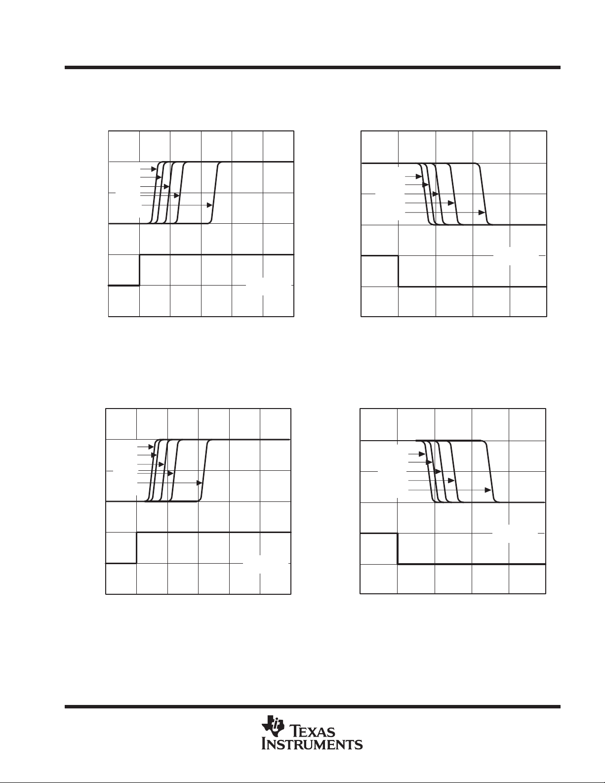
TYPICAL CHARACTERISTICS
LOW-TO HIGH-LEVEL OUTPUT
RESPONSE FOR VARIOUS INPUT OVERDRIVES
4.5
3
40 mV
20 mV
10 mV
1.5
5 mV
– Output Voltage – VV
O
– InputV
I(STEP)
Voltage Step – mV
2 mV
0
100
0
0 0.5 1 1.5 2 2.5
Low-to High-Level Output Response Time – µs
Figure 1
LOW-TO HIGH-LEVEL OUTPUT
RESPONSE FOR VARIOUS INPUT OVERDRIVES
7.5
VCC = 3 V
TA = 25° C
HIGH-TO LOW-LEVEL OUTPUT
RESPONSE FOR VARIOUS INPUT OVERDRIVES
4.5
3
40 mV
1.5
– Output Voltage – VV
O
100
– InputV
I(STEP)
Voltage Step – mV
20 mV
10 mV
5 mV
2 mV
0
VCC = 3 V
TA = 25° C
0
0 0.2 0.4 0.6 0.8
High-to Low-Level Output Response Time – µs
Figure 2
HIGH-TO LOW-LEVEL OUTPUT
RESPONSE FOR VARIOUS INPUT OVERDRIVES
7.5
5
40 mV
20 mV
10 mV
2.5
– Output Voltage – VV
OVoltage Step – mV
0
100
– InputV
0
I(STEP)
Low-to High-Level Output Response Time – µs
5 mV
2 mV
VCC = 5 V
TA = 25° C
0 0.5 1 1.5 2 2.5
Figure 3
5
2.5
– Output Voltage – VV
O
0
100
– InputV
0
I(STEP)
Voltage Step – mV
High-to Low-Level Output Response Time – µs
40 mV
20 mV
10 mV
5 mV
2 mV
VCC = 5 V
TA = 25° C
0 0.2 0.4 0.6 0.8
Figure 4
POST OFFICE BOX 655303 • DALLAS, TEXAS 75265
9

IMPORTANT NOTICE
T exas Instruments and its subsidiaries (TI) reserve the right to make changes to their products or to discontinue
any product or service without notice, and advise customers to obtain the latest version of relevant information
to verify, before placing orders, that information being relied on is current and complete. All products are sold
subject to the terms and conditions of sale supplied at the time of order acknowledgement, including those
pertaining to warranty, patent infringement, and limitation of liability.
TI warrants performance of its semiconductor products to the specifications applicable at the time of sale in
accordance with TI’s standard warranty. Testing and other quality control techniques are utilized to the extent
TI deems necessary to support this warranty . Specific testing of all parameters of each device is not necessarily
performed, except those mandated by government requirements.
CERT AIN APPLICATIONS USING SEMICONDUCTOR PRODUCTS MAY INVOLVE POTENTIAL RISKS OF
DEATH, PERSONAL INJURY, OR SEVERE PROPERTY OR ENVIRONMENTAL DAMAGE (“CRITICAL
APPLICATIONS”). TI SEMICONDUCTOR PRODUCTS ARE NOT DESIGNED, AUTHORIZED, OR
WARRANTED TO BE SUITABLE FOR USE IN LIFE-SUPPORT DEVICES OR SYSTEMS OR OTHER
CRITICAL APPLICA TIONS. INCLUSION OF TI PRODUCTS IN SUCH APPLICATIONS IS UNDERST OOD TO
BE FULLY AT THE CUSTOMER’S RISK.
In order to minimize risks associated with the customer’s applications, adequate design and operating
safeguards must be provided by the customer to minimize inherent or procedural hazards.
TI assumes no liability for applications assistance or customer product design. TI does not warrant or represent
that any license, either express or implied, is granted under any patent right, copyright, mask work right, or other
intellectual property right of TI covering or relating to any combination, machine, or process in which such
semiconductor products or services might be or are used. TI’s publication of information regarding any third
party’s products or services does not constitute TI’s approval, warranty or endorsement thereof.
Copyright 1999, Texas Instruments Incorporated
 Loading...