

Datasheet TLV0831IDR, TLV0831CP, TLV0831ID, TLV0831CDR, TLV0831CD Datasheet (Texas Instruments)
...
TLV0831C, TLV0831I
TLV0832C, TLV0832I
3-VOLT 8-BIT ANALOG-TO-DIGITAL CONVERTERS WITH SERIAL CONTROL
SLAS148 – SEPTEMBER 1996
1
POST OFFICE BOX 655303 • DALLAS, TEXAS 75265
D
8-Bit Resolution
D
2.7 V to 3.6 V V
CC
D
Easy Microprocessor Interface or
Standalone Operation
D
Operates Ratiometrically or With V
CC
Reference
D
Single Channel or Multiplexed Twin
Channels With Single-Ended or Differential
Input Options
D
Input Range 0 V to VCC With VCC Reference
D
Inputs and Outputs Are Compatible With
TTL and MOS
D
Conversion Time of 32 µs at
f
(CLK)
= 250 kHz
D
Designed to Be Functionally Equivalent to
the National Semiconductor ADC0831 and
ADC0832 at 3 V Supply
D
T otal Unadjusted Error...±1 LSB
description
These devices are 8-bit successive-approximation analog-to-digital converters. The TL V0831 has single input
channels; the TLV0832 has multiplexed twin input channels. The serial output is configured to interface with
standard shift registers or microprocessors.
The TL V0832 multiplexer is software configured for single-ended or dif ferential inputs. The dif ferential analog
voltage input allows for common-mode rejection or offset of the analog zero input voltage value. In addition, the
voltage reference input can be adjusted to allow encoding any smaller analog voltage span to the full 8 bits of
resolution.
The operation of the TL V0831 and TLV0832 devices is very similar to the more complex TL V0834 and TL V0838
devices. Ratiometric conversion can be attained by setting the REF input equal to the maximum analog input
signal value, which gives the highest possible conversion resolution. Typically, REF is set equal to V
CC
(done
internally on the TLV0832).
The TL V0831C and TL V0832C are characterized for operation from 0°C to 70°C. The TL V0831I and TL V0832I
are characterized for operation from –40°C to 85°C.
AVAILABLE OPTIONS
PACKAGE
T
A
SMALL OUTLINE
(D)
PLASTIC DIP
(P)
0°C to 70°C TLV0831CD TLV0832CD TLV0831CP TLV0832CP
–40°C to 85°C TLV0831ID TLV0832ID TLV0831IP TLV0832IP
Please be aware that an important notice concerning availability, standard warranty, and use in critical applications of
Texas Instruments semiconductor products and disclaimers thereto appears at the end of this data sheet.
1
2
3
4
8
7
6
5
CS
IN+
IN–
GND
V
CC
CLK
DO
REF
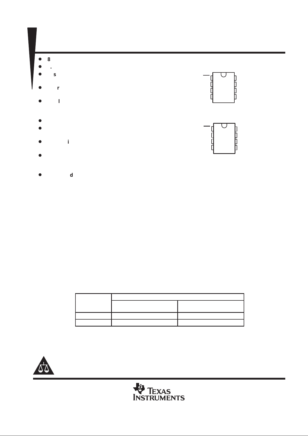
TLV0831...D OR P PACKAGE
(TOP VIEW)
1
2
3
4
8
7
6
5
CS
CH0
CH1
GND
V
CC
/REF
CLK
DO
DI
TLV0832...D OR P PACKAGE
(TOP VIEW)
PRODUCTION DATA information is current as of publication date.
Products conform to specifications per the terms of Texas Instruments
standard warranty. Production processing does not necessarily include
testing of all parameters.
Copyright 1996, Texas Instruments Incorporated
TLV0831C, TLV0831I
TLV0832C, TLV0832I
3-VOLT 8-BIT ANALOG-TO-DIGITAL CONVERTERS WITH SERIAL CONTROL
SLAS148 – SEPTEMBER 1996
2
POST OFFICE BOX 655303 • DALLAS, TEXAS 75265
functional block diagram
R
Start
Flip-Flop
S
CLK
CLK
Time
Delay
S
R
CS
DO
CS
CS
D
CLK
R
EOC
9-Bit
Shift
Register
CS
R
CLK
First
LSB
Bit 1
Bits 0–7
First
One
Shot
SAR
Logic
and
Latch
R
EN
CS
Bits 0–7
REF
Ladder
and
Decoder
EN
Comparator
EN
Analog
MUX
CH1/IN–
CH0/IN+
SGL/DIF
ODD/EVEN
Start
CLK
D
Shift Register
To Internal
Circuits
(TLV0832
only)
DI
CS
CLK
MSB
(TLV0831
only)

TLV0831C, TLV0831I
TLV0832C, TLV0832I
3-VOLT 8-BIT ANALOG-TO-DIGITAL CONVERTERS WITH SERIAL CONTROL
SLAS148 – SEPTEMBER 1996
3
POST OFFICE BOX 655303 • DALLAS, TEXAS 75265
functional description
The TL V0831 and TL V0832 use a sample-data-comparator structure that converts differential analog inputs by
a successive-approximation routine. The input voltage to be converted is applied to an input terminal and is
compared to ground (single ended), or to an adjacent input (differential). The TL V0832 input terminals can be
assigned a positive (+) or negative (–) polarity . The TLV0831 contains only one differential input channel with
fixed polarity assignment; therefore it does not require addressing. The signal can be applied differentially,
between IN+ and IN–, to the TL V0831 or can be applied to IN+ with IN– grounded as a single ended input. When
the signal input applied to the assigned positive terminal is less than the signal on the negative terminal, the
converter output is all zeros.
Channel selection and input configuration are under software control using a serial-data link from the controlling
processor. A serial-communication format allows more functions to be included in a converter package with no
increase in size. In addition, it eliminates the transmission of low-level analog signals by locating the converter
at the analog sensor and communicating serially with the controlling processor. This process returns noise-free
digital data to the processor.
A conversion is initiated by setting CS
low, which enables all logic circuits. CS must be held low for the complete
conversion process. A clock input is then received from the processor. An interval of one clock period is
automatically inserted to allow the selected multiplexed channel to settle. DO comes out of the high-impedance
state and provides a leading low for one clock period of multiplexer settling time. The SAR comparator compares
successive outputs from the resistive ladder with the incoming analog signal. The comparator output indicates
whether the analog input is greater than or less than the resistive-ladder output. As the conversion proceeds,
conversion data is simultaneously output from DO, with the most significant bit (MSB) first. After eight clock
periods, the conversion is complete. When CS
goes high, all internal registers are cleared. At this time, the
output circuits go to the high-impedance state. If another conversion is desired, CS
must make a high-to-low
transition followed by address information.
A TLV0832 input configuration is assigned during the multiplexer-addressing sequence. The multiplexer
address shifts into the converter through the data input (DI) line. The multiplexer address selects the analog
inputs to be enabled and determines whether the input is single ended or differential. When the input is
differential, the polarity of the channel input is assigned. In addition to selecting the differential mode, the polarity
may also be selected. Either channel of the channel pair may be designated as the negative or positive input.
On each low-to-high transition of the clock input, the data on DI is clocked into the multiplexer-address shift
register. The first logic high on the input is the start bit. A 2-bit assignment word follows the start bit on the
TLV0832. On each successive low-to-high transition of the clock input, the start bit and assignment word are
shifted through the shift register. When the start bit is shifted into the start location of the multiplexer register,
the input channel is selected and conversion starts. The TLV0832 DI terminal to the multiplexer shift register
is disabled for the duration of the conversion.
The TL V0832 outputs the least-significant-bit (LSB) first data after the MSB-first data stream. The DI and DO
terminals can be tied together and controlled by a bidirectional processor I/O bit received on a single wire. This
is possible because DI is only examined during the multiplexer-addressing interval and DO is still in the
high-impedance state.
TLV0831C, TLV0831I
TLV0832C, TLV0832I
3-VOLT 8-BIT ANALOG-TO-DIGITAL CONVERTERS WITH SERIAL CONTROL
SLAS148 – SEPTEMBER 1996
4
POST OFFICE BOX 655303 • DALLAS, TEXAS 75265
sequence of operation
Don’t Care
176201267
MSBLSB
LSB-First Data
EVEN
DIF
+Sign Bit
ODD
SGL
Start
Bit
1765 243
MSB
DI
DO
CS
t
su
CLK
21201918141312123456 1011
TLV0832
Hi-Z
0
LSB
t
conv
MSB-First Data
MSB
Hi-Z
DO
MUX
Settling Time
CS
CLK
10987654321
t
su
t
conv
TLV0831
Hi-Z
MSB-First Data
TLV0832 MUX-ADDRESS CONTROL LOGIC TABLE
MUX ADDRESS
CHANNEL NUMBER
SGL/DIF
ODD/EVEN CH0 CH1
L
H
L
H
L
L
H
H
+
–
+
–
+
+
MUX
Settling Time
H = high level, L = low level,
– or + = terminal polarity for the selected input channel
(TLV0832
only)

TLV0831C, TLV0831I
TLV0832C, TLV0832I
3-VOLT 8-BIT ANALOG-TO-DIGITAL CONVERTERS WITH SERIAL CONTROL
SLAS148 – SEPTEMBER 1996
5
POST OFFICE BOX 655303 • DALLAS, TEXAS 75265
absolute maximum ratings over recommended operating free-air temperature range (unless
otherwise noted)
†
Supply voltage, V
CC
(see Note 1) 6.5 V. . . . . . . . . . . . . . . . . . . . . . . . . . . . . . . . . . . . . . . . . . . . . . . . . . . . . . . . . . .
Input voltage range, V
I
: Logic –0.3 V to VCC + 0.3 V. . . . . . . . . . . . . . . . . . . . . . . . . . . . . . . . . . . . . . . . . . . . . . .
Analog –0.3 V to V
CC
+ 0.3 V. . . . . . . . . . . . . . . . . . . . . . . . . . . . . . . . . . . . . . . . . . . . . .
Input current, I
I
±5 mA. . . . . . . . . . . . . . . . . . . . . . . . . . . . . . . . . . . . . . . . . . . . . . . . . . . . . . . . . . . . . . . . . . . . . . . . . .
Total input current ±20 mA. . . . . . . . . . . . . . . . . . . . . . . . . . . . . . . . . . . . . . . . . . . . . . . . . . . . . . . . . . . . . . . . . . . . . . .
Operating free-air temperature range, T
A
: C suffix 0°C to 70°C. . . . . . . . . . . . . . . . . . . . . . . . . . . . . . . . . . . . . .
I suffix –40°C to 85°C. . . . . . . . . . . . . . . . . . . . . . . . . . . . . . . . . . . . .
Storage temperature range, T
stg
–65°C to 150°C. . . . . . . . . . . . . . . . . . . . . . . . . . . . . . . . . . . . . . . . . . . . . . . . . . .
Lead temperature 1,6 mm (1/16 inch) from case for 10 seconds: P package 260°C. . . . . . . . . . . . . . . . . . . . .
†
Stresses beyond those listed under “absolute maximum ratings” may cause permanent damage to the device. These are stress ratings only, and
functional operation of the device at these or any other conditions beyond those indicated under “recommended operating conditions” is not
implied. Exposure to absolute-maximum-rated conditions for extended periods may affect device reliability.
NOTE 1: All voltage values, except differential voltages, are with respect to the network ground terminal.
recommended operating conditions
MIN NOM MAX UNIT
Supply voltage, VCC (see clock operating conditions) 2.7 3.3 3.6 V
High-level input voltage, V
IH
2 V
Low-level input voltage, V
IL
0.8 V
VCC = 2.7 V 250 kHz
Clock frequenc
y,
f
(CLK)
VCC = 3.3 V 10 600 kHz
Clock duty cycle (see Note 2) 40% 60%
Pulse duration, CS high, t
wH(CS)
220 ns
Setup time, CS low or TLV0832 data valid before CLK↑, t
su
350 ns
Hold time, TLV0832 data valid after CLK↑, t
h
90 ns
p
p
C suffix 0 70
°
Operating free-air temperature, T
A
I suffix –40 85
°C
NOTE 2: The clock-duty-cycle range ensures proper operation at all clock frequencies. When a clock frequency is used outside the
recommended duty-cycle range, the minimum pulse duration (high or low) is 1 µs.

TLV0831C, TLV0831I
TLV0832C, TLV0832I
3-VOLT 8-BIT ANALOG-TO-DIGITAL CONVERTERS WITH SERIAL CONTROL
SLAS148 – SEPTEMBER 1996
6
POST OFFICE BOX 655303 • DALLAS, TEXAS 75265
electrical characteristics over recommended range of operating free-air temperature, VCC = 3.3 V ,
f
(CLK)
= 250 kHz (unless otherwise noted)
digital section
C SUFFIX I SUFFIX
PARAMETER
TEST CONDITIONS
†
MIN TYP‡MAX MIN TYP‡MAX
UNIT
p
VCC = 3 V, IOH = –360 µA 2.8 2.4
VOHHigh-level output voltage
VCC = 3 V, IOH = –10 µA 2.9 2.8
V
V
OL
Low-level output voltage VCC = 3 V, IOL = 1.6 mA 0.34 0.4 V
I
IH
High-level input current VIH = 3.6 V 0.005 1 0.005 1 µA
I
IL
Low-level input current VIL = 0 –0.005 –1 –0.005 –1 µA
I
OH
High-level output
(source) current
At VOH, DO= 0 V, TA = 25°C –6.5 –15 –6.5 –15 mA
I
OL
Low-level output (sink) current At VOL, DO= 0 V, TA = 25°C 8 –16 8 –16 mA
High-impedance-state output
VO = 3.3 V, TA = 25°C 0.01 3 0.01 3
I
OZ
g
current (DO)
VO = 0, TA = 25°C
–0.01 –3 –0.01 –3
µ
A
C
i
Input capacitance 5 5 pF
C
o
Output capacitance 5 5 pF
†
All parameters are measured under open-loop conditions with zero common-mode input voltage.
‡
All typical values are at VCC = 3.3 V, TA = 25°C.
analog and converter section
PARAMETER TEST CONDITIONS
†
MIN TYP‡MAX UNIT
V
IC
Common-mode input voltage See Note 3
–0.05
to
VCC+0.05
V
On channel VI = 3.3 V 1
p
Off channel VI = 0 –1
I
I(stdby)
Standby input current (see Note 4)
On channel VI = 0 –1
µ
A
Off channel VI = 3.3 V 1
r
i(REF)
Input resistance to REF 1.3 2.4 5.9 kΩ
†
All parameters are measured under open-loop conditions with zero common-mode input voltage.
‡
All typical values are at VCC = 3.3 V, TA = 25°C.
NOTES: 3. When channel IN– is more positive than channel IN+, the digital output code is 0000 0000. Connected to each analog input are two
on-chip diodes that conduct forward current for analog input voltages one diode drop above VCC. Care must be taken during testing
at low VCC levels (3 V) because high-level analog input voltage (3.6 V) can, especially at high temperatures, cause the input diode
to conduct and cause errors for analog inputs that are near full scale. As long as the analog voltage does not exceed the supply
voltage by more than 50 mV, the output code is correct. To achieve an absolute 0- to 3.3-V input range requires a minimum VCC of
3.25 V for all variations of temperature and load.
4. Standby input currents go in or out of the on or off channels when the A/D converter is not performing conversion and the clock is
in a high or low steady-state conditions.
total device
PARAMETER MIN TYP‡MAX UNIT
pp
TLV0831 0.2 0.75
I
CC
Supply current
TLV0832 1.5 2.5
mA
‡
All typical values are at VCC = 3.3 V, TA = 25°C.

TLV0831C, TLV0831I
TLV0832C, TLV0832I
3-VOLT 8-BIT ANALOG-TO-DIGITAL CONVERTERS WITH SERIAL CONTROL
SLAS148 – SEPTEMBER 1996
7
POST OFFICE BOX 655303 • DALLAS, TEXAS 75265
operating characteristics VCC = V
ref
= 3.3 V, f
(CLK)
= 250 kHz, tr = tf = 20 ns, TA = 25°C (unless
otherwise noted)
PARAMETER
TEST CONDITIONS
†
MIN TYP MAX UNIT
Supply-voltage variation error VCC = 3 V to 3.6 V ±1/16 ±1/4 LSB
Total unadjusted error (see Note 5)
V
ref
= 3.3 V,
TA = MIN to MAX
±1 LSB
Common-mode error Differential mode ±1/16 ±1/4 LSB
Propagation delay time,
p
MSB-first data
p
200 500
t
pd
output data after
CLK↑
(see Note 6)
LSB-first data
C
L
=
100 pF
80 200
ns
CL = 10 pF, RL = 10 kΩ 80 125
t
dis
Output disable ti
me, DO after
CS↑
CL = 100 pF, RL = 2 kΩ 250
ns
t
conv
Conversion time (multiplexer-addressing
time not included)
8
clock
periods
†
All parameters are measured under open-loop conditions with zero common-mode input voltage. For conditions shown as MIN or MAX, use the
appropriate value specified under recommended operating conditions.
NOTES: 5. Total unadjusted error includes offset, full-scale, linearity, and multiplexer errors.
6. The MSB-first data is output directly from the comparator and, therefore, requires additional delay to allow for comparator response
time. LSB-first data applies only to TLV0832.

TLV0831C, TLV0831I
TLV0832C, TLV0832I
3-VOLT 8-BIT ANALOG-TO-DIGITAL CONVERTERS WITH SERIAL CONTROL
SLAS148 – SEPTEMBER 1996
8
POST OFFICE BOX 655303 • DALLAS, TEXAS 75265
PARAMETER MEASUREMENT INFORMATION
50%
t
pd
50%
GND
V
OL
V
OH
V
CC
CLK
DO
50%
t
su
t
h
t
h
t
su
50%
V
CC
GND
GND
GND
0.4 V0.4 V
2 V
2 V
DI
0.4 V
CS
CLK
V
CC
V
CC
Figure 1. TLV0832 Data-Input Timing
Figure 2. Data-Output Timing
VOLTAGE WAVEFORMS
S2 open
S1 closed
10%
10%
90%
t
r
VOLTAGE WAVEFORMS
S2 closed
S1 open
DO
Output
t
r
S1
S2
LOAD CIRCUIT
(see Note A)
C
L
From Output
Under Test
Test
Point
CS
CS
t
dis
90%
10%
90%
50%
50%
V
CC
GND
GND
GND
GND
V
CC
V
CC
V
CC
V
CC
R
L
DO
Output
t
dis
NOTE A: CL includes probe and jig capacitance.
Figure 3. Output Disable Time Test Circuit and Voltage Waveforms

TLV0831C, TLV0831I
TLV0832C, TLV0832I
3-VOLT 8-BIT ANALOG-TO-DIGITAL CONVERTERS WITH SERIAL CONTROL
SLAS148 – SEPTEMBER 1996
9
POST OFFICE BOX 655303 • DALLAS, TEXAS 75265
TYPICAL CHARACTERISTICS
V
ref –
Reference Voltage – VV
ref
– Reference V oltage – V
VCC = 3.3 V
f
(CLK)
= 250 kHz
TA = 25°C
4321
0
0.25
0.5
0.75
1.0
1.25
0
1.5
101.00.10.01
VI+ = VI– = 0 V
0
2
4
6
8
10
12
14
16
UNADJUSTED OFFSET ERROR
vs
REFERENCE VOLTAGE
LINEARITY ERROR
vs
REFERENCE VOLTAGE
E
O(unadj)
– Unadjusted Offset Error – LSB
– Linearity Error – LSB
E
L
Figure 4 Figure 5
f
(
CLK
)
– Clock Frequency – kHzTA – Free-Air Tempertature – °C
V
ref
= 3.3 V
f
(CLK)
= 250 kHz
1007550250–25
0.5
0.45
0.4
0.35
0.3
–50
0.25
LINEARITY ERROR
vs
FREE-AIR TEMPERATURE
LINEARITY ERROR
vs
CLOCK FREQUENCY
– Linearity Error – LSB
E
L
– Linearity Error – LSB
E
L
600500400300200100
2.0
1.8
1.2
1
0.8
0.2
0
0
85°C
25°C
–40°C
V
ref
= 3.3 V
VCC = 3.3 V
1.6
1.4
0.6
0.4
700 800
Figure 6 Figure 7
TLV0831C, TLV0831I
TLV0832C, TLV0832I
3-VOLT 8-BIT ANALOG-TO-DIGITAL CONVERTERS WITH SERIAL CONTROL
SLAS148 – SEPTEMBER 1996
10
POST OFFICE BOX 655303 • DALLAS, TEXAS 75265
TYPICAL CHARACTERISTICS
f
(
CLK
)
– Clock Frequency – kHzTA – Free-Air Temperature — °C
f
(CLK)
= 250 kHz
CS
= High
VCC = 3.6 V
VCC = 3 V
1007550250–25
0.3
0.2
–50
0.1
– Supply Current – mA
TLV0831
SUPPLY CURRENT
vs
FREE-AIR TEMPERATURE
TLV0831
SUPPLY CURRENT
vs
CLOCK FREQUENCY
CC
I
– Supply Current – mA
CC
I
VCC = 3.3 V
VCC = 3.3 V
TA = 25°C
5004003002001000
0
0.1
0.2
0.3
0.4
0.5
Figure 8 Figure 9
TA – Free-Air Temperature – °C
VCC = 3.3 V
IOL
(DO = 0.4 V)
16
16.5
15.5
15
14.5
1007550250–25–50
14
– Output Current – mA
OUTPUT CURRENT
vs
FREE-AIR TEMPERATURE
I
O
IOL
(DO = 3.3 V)
–IOH
(DO = 0 V)
–IOH
(DO = 2.4 V)
Figure 10
TLV0831C, TLV0831I
TLV0832C, TLV0832I
3-VOLT 8-BIT ANALOG-TO-DIGITAL CONVERTERS WITH SERIAL CONTROL
SLAS148 – SEPTEMBER 1996
11
POST OFFICE BOX 655303 • DALLAS, TEXAS 75265
TYPICAL CHARACTERISTICS
Differential Nonlinearity – LSB
–1
Output Code
1
0.5
0
–0.5
0 32 64 96 128 160 192 224 256
V
ref
= 3.3 V
TA = 25°C
F
(CLK)
= 250 kHz
VDD = 3.3 V
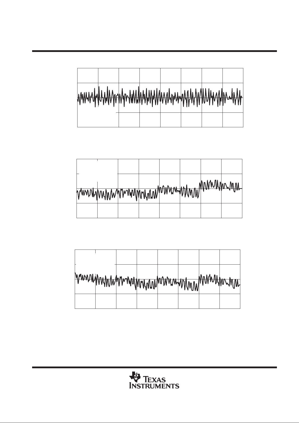
Figure 11. Differential Nonlinearity With Output Code
Integral Nonlinearity – LSB
–1
Output Code
1
0.5
0
–0.5
0 32 64 96 128 160 192 224 256
V
ref
= 3.3 V
TA = 25°C
F
(CLK)
= 250 kHz
VDD = 3.3 V
Figure 12. Integral Nonlinearity With Output Code
Total Unadjusted Error – LSB
–1
Output Code
1
0.5
0
–0.5
0 32 64 96 128 160 192 224 256
V
ref
= 3.3 V
TA = 25°C
F
(CLK)
= 250 kHz
VDD = 3.3 V
Figure 13. Total Unadjusted Error With Output Code

IMPORTANT NOTICE
T exas Instruments and its subsidiaries (TI) reserve the right to make changes to their products or to discontinue
any product or service without notice, and advise customers to obtain the latest version of relevant information
to verify, before placing orders, that information being relied on is current and complete. All products are sold
subject to the terms and conditions of sale supplied at the time of order acknowledgement, including those
pertaining to warranty, patent infringement, and limitation of liability.
TI warrants performance of its semiconductor products to the specifications applicable at the time of sale in
accordance with TI’s standard warranty. Testing and other quality control techniques are utilized to the extent
TI deems necessary to support this warranty. Specific testing of all parameters of each device is not necessarily
performed, except those mandated by government requirements.
CERT AIN APPLICATIONS USING SEMICONDUCTOR PRODUCTS MAY INVOLVE POTENTIAL RISKS OF
DEATH, PERSONAL INJURY, OR SEVERE PROPERTY OR ENVIRONMENTAL DAMAGE (“CRITICAL
APPLICATIONS”). TI SEMICONDUCTOR PRODUCTS ARE NOT DESIGNED, AUTHORIZED, OR
WARRANTED TO BE SUITABLE FOR USE IN LIFE-SUPPORT DEVICES OR SYSTEMS OR OTHER
CRITICAL APPLICATIONS. INCLUSION OF TI PRODUCTS IN SUCH APPLICA TIONS IS UNDERST OOD TO
BE FULLY AT THE CUSTOMER’S RISK.
In order to minimize risks associated with the customer’s applications, adequate design and operating
safeguards must be provided by the customer to minimize inherent or procedural hazards.
TI assumes no liability for applications assistance or customer product design. TI does not warrant or represent
that any license, either express or implied, is granted under any patent right, copyright, mask work right, or other
intellectual property right of TI covering or relating to any combination, machine, or process in which such
semiconductor products or services might be or are used. TI’s publication of information regarding any third
party’s products or services does not constitute TI’s approval, warranty or endorsement thereof.
Copyright 1998, Texas Instruments Incorporated
 Loading...