

Page 1
User’s Guide Rev 0.1
SLLU104A - September 2007
September 2007
TLK3134 XAUI Transceiver / 4 Channel Multi-Rate
Transceiver Evaluation Module (EVM) Users’ Guide
ABSTRACT
This User’s Guide describes the usage and construction of the TLK3134 evaluation module
(EVM). This document provides guidance on proper use by showing some de
and test modes. In addition, design, layout and schematic information is provided to the
customer. Information in this guide can be used to assist the customer in choosing the optimal
design methods and materials in designing a complete system.
vice configurations
This equipment is intended for use in a laboratory test environment only. It generates, uses, and can radiate radio frequency energy
and has not bee
designed to provide reasonable protection against radio frequency interference. Operation of this equipment in other environments
may cause interference with radio communications, in which case the user at own expense will be required to take whatever
measures may be required to correct this interference.
n tested for compliance with the limits of computing devices pursuant to subpart J of part 15 of FCC rules, which are
WARNING
1
Page 2

SLLU104A - September 2007
Contents
Introduction.................................................................................................................................................... 4
TLK3134 EVM Kit Contents........................................................................................................................... 5
Power .............................................................................................................................................................. 6
Power Monitoring LEDs ................................................................................................................................ 9
Control Signals ............................................................................................................................................ 12
MDIO ............................................................................................................................................................. 16
JTAG ............................................................................................................................................................. 17
Reset ............................................................................................................................................................. 18
Parallel Signals ............................................................................................................................................ 19
XAUI Mode (XGMII) Test and Setup Configuration ................................................................................... 21
Gigabit Ethernet Mode (RGMII) Test and Setup Configuration ............................................................... 24
Schematics................................................................................................................................................... 27
Board Layouts.............................................................................................................................................. 45
Figures
Figure 1. TLK3134 EVM Power Source Selection Example.....................................................................6
Figure 2. TLK3134 EVM VDDM Voltage Source Selection.......................................................................6
Figure 3. TLK3134 EVM VDDM Voltage Source Selection.......................................................................7
Figure 4. TLK3134 EVM Regulator Margin Selection...............................................................................7
Figure 5. TLK3134 EVM Voltage Monitor LED Enabled Example ...........................................................9
Figure 6. TLK3134 EVM Voltage Monitor LED Disabled Example ........................................................10
Figure 7. TLK3134 EVM Voltage Monitor LED Connected Directly to Plane Example........................10
Figure 8. Control Connectors (JMP13, JMP15, JMP20, JMP21, JMP25, JMP26).................................12
Figure 9. TLK3134 EVM MDIO Connector (JMP22) ................................................................................16
Figure 10. TLK3134 EVM JTAG Connector (JMP23).............................................................................17
Figure 11. RESET Switch (SW1, JMP10, or JMP11)..............................................................................18
Figure 12. Parallel Signal Header Block Example.................................................................................19
Figure 13. Parallel Signal Header Block Example.................................................................................19
Figure 14. Parallel Loop Back with Static Data Pattern Example........................................................20
Figure 15. Parallel Loop Back with Static Data Pattern Example........................................................20
Figure 16. Example TLK3134 EVM Test Configuration – XAUI Mode (XGMII) Parallel Loopback ....23
Figure 17. Example TLK3134 EVM Test Configuration – Gigabit Ethernet Mode (RGMII) Serial
Loopback ................................................................................................................................................26
Figure 18. TLK3134 EVM Schematic, Sheet 1 Index .............................................................................27
Figure 19. TLK3134 EVM Schematic, Sheet 2 Device Power and Ground..........................................28
Figure 20. TLK3134 EVM Schematic, Sheet 3 Global Signals .............................................................29
Figure 21. TLK3134 EVM Schematic, Sheet 4 High Speed Differential...............................................30
Figure 22. TLK3134 EVM Schematic, Sheet 5 Jitter Cleaner Clock.....................................................31
Figure 23. TLK3134 EVM Schematic, Sheet 6 JTAG and MDIO ...........................................................32
Figure 24. TLK3134 EVM Schematic, Sheet 7 TX and RX Data Lines .................................................33
Figure 25. TLK3134 EVM Schematic, Sheet 8 TX/RX Clocks and Control..........................................34
Figure 26. TLK3134 EVM Schematic, Sheet 9 Power Regulation ........................................................35
Figure 27. TLK3134 EVM Schematic, Sheet 10 Power Distribution ....................................................36
Figure 28. TLK3134 EVM Schematic, Sheet 11 1P2V and 2P5V Supply LEDs ...................................37
Figure 29. TLK3134 EVM Schematic, Sheet 12 1P5V, 1P8V, and 5V Supply LEDs............................38
Figure 30. TLK3134 EVM Schematic, Sheet 13 VDDM Supply LEDs...................................................39
Figure 31. TLK3134 EVM Schematic, Sheet 14 VDDR Supply LEDs ...................................................40
Figure 32. TLK3134 EVM Schematic, Sheet 15 VREF Supply LEDs....................................................41
Figure 33. TLK3134 EVM Schematic, Sheet 16 VJIT Supply LEDs......................................................42
Figure 34. TLK3134 EVM Layout, Top Signal (Layer 1) ........................................................................45
2 TLK3134 XAUI Transceiver / 4 Channel Multi-Rate Transceiver Evaluation Module (EVM) Users’ Guide
Page 3

Figure 35. TLK3134 EVM Layout, Ground (Layers 2,4,6,8,10,11) .......................................................46
SLLU104A - September 2007
Figure 36. TLK3134 EVM Layout, Internal Signal (Layer 3).................................................................47
Figure 37. TLK3134 EVM Layout, Internal Signal (Layer 5).................................................................48
Figure 38. TLK3134 EVM Layout, Power (Layer 7)................................................................................49
Figure 39. TLK3134 EVM Layout, Power (Layer 9)................................................................................50
Figure 40. TLK3134 EVM Layout, Internal Signal (Layer 12)...............................................................51
Figure 41. TLK3134 EVM Layout, Ground (Layer 13) ...........................................................................52
Figure 42. TLK3134 EVM Layout, Internal Signal (Layer 14)................................................................53
Figure 43. TLK3134 EVM Layout, Ground (Layers 15) .........................................................................54
Figure 44. TLK3134 EVM Layout, Bottom Signal (Layers 16) ..............................................................55
TLK3134 EVM Layer Construction ..............................................................................................................56
Tables
Table 1. TLK3134 EVM Bill of Materials.................................................................................................43
.
TLK3134 XAUI Transceiver / 4 Channel Multi-Rate Transceiver Evaluation Module (EVM) Users’ Guide 3
Page 4

SLLU104A - September 2007
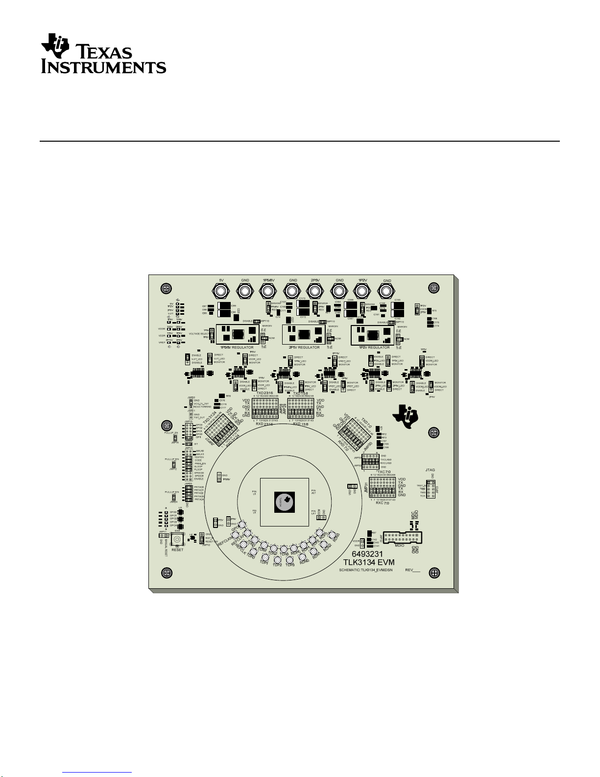
Introduction
The Texas Instruments (TI™) TLK3134 SerDes evaluation module (EVM) board is used to
evaluate the functionality and the performance of TLK3134 XAUI Transceiver/4 Channel MultiRate Transceiver device (289-ball BGA). The TLK3134 is a flexible four channel independently
configurable serial transceiver that can be configured to be compliant with the 10Gbps Ethernet
XAUI Specification, the 1000Base-X 1Gbps Ethernet Specification and will also support
1X/2X/10X Fibre Channel (FC), CPRI (x1/x2/x3), OBSAI (x1/x2/x4) data rates. Many common
applications may be enabled by way of externally available control pins and detailed control of
the TLK3134 on a per channel basis is available by way of accessing a register space of control
bits available through a two-wire access port called the Management Data Input/Output (MDIO)
interface.
1
EVM PCB and High-speed Design Considerations
The board can be used to evaluate device parameters in addition to acting as a guide for highspeed board layout. As the frequency of op
special care to ensure that the highest signal integrity is maintained. To achieve this, the board's
impedance is controlled to 50 Ω for both the high-speed differential serial and low-speed parallel
data and clock connections. Vias are minimized and, when necessary, are designed to minimize
impedance discontinuities along the transmission line. Since the board contains both, serial and
parallel transmission lines, care was taken also to control trace length mismatch (board skew) to
less than +/- 1MIL.
Overall, the board layout is designed and optimized to support high-speed operation. Thus,
understanding impedance control and transmission line eff
speed boards. Some of the advanced features offered by this board include:
• PCB (printed circuit board) is designed for optimal high-speed signal integrity.
• SMP and parallel header fixtures are easily connected to test equipment.
• All input/output signals are accessible for rapid prototyping.
• The entire board can be powered from a single 5V power supply where the power planes
can be supplied through on-board regulators or t
• On-board capacitors provide AC coupling of high-speed receive signals.
• External parallel loop-back function can be achieved easily using simple 0.1 inch jumpers.
eration increases, the board designer must take
ects are crucial when designing high-
hrough separate banana jacks for isolation.
• Entire Board can operate from a single 5V power supply, or from individual power supplies.
•
Voltage Monitoring LED circuits provide quick indication that the voltage is within
specification.
1
The MDIO register map is located within the TLK3134 XAUI Transceiver/4 Channel Multi-Rate Transceiver datasheet.
4 TLK3134 XAUI Transceiver / 4 Channel Multi-Rate Transceiver Evaluation Module (EVM) Users’ Guide
Page 5

SLLU104A - September 2007
TLK3134 EVM Kit Contents
The TLK3134 EVM kit contains the following:
• TLK3134 EVM board
• TLK3134 EVM User’s Guide (this document)
• TLK3134 XAUI Transceiver/4 Channel Multi-Rate Transceiver datasheet
• MDIO Interface EVM
• MDIO Interface EVM Documentation
• RS-232 Cable
• 20-conductor MDIO Ribbon Cable
• CD-ROM Containing MDIO Software
• 18 3-Foot SMA to SMP cables
.
• 8 1-Foot SMP to SMP cables
TLK3134 XAUI Transceiver / 4 Channel Multi-Rate Transceiver Evaluation Module (EVM) Users’ Guide 5
Page 6
SLLU104A - September 2007
Power
The TLK3134 EVM can be operated off of a single 5V Power Supply utilizing the on-board
voltage regulators to generate the voltages required to correctly operate the TLK3134, off of
individual 1.2V, 1.5V or 1.8V, 2.5V, and 5V Power supplies, or a combination of both regulators
and separate individual supplies.
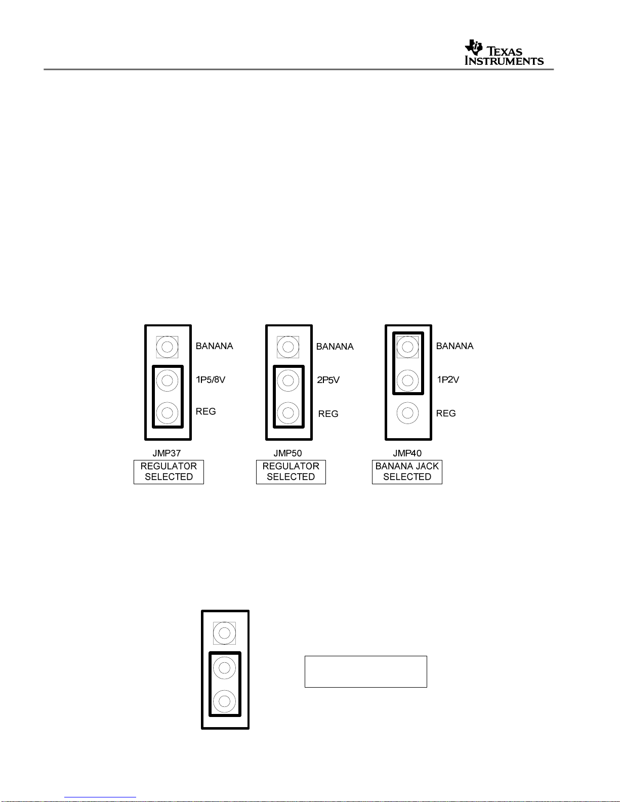
To modify your power supply configuration between either all Individual Supplies, all on-board
regulators, or a combinat
supply headers (JMP37, JMP40, and JMP50) selecting either the “BANANA” or the “REG” pin in
combination with the center pin. The following figure shows how to use the on-board regulators
for the 1.5V or 1.8V and 2.5V supply rails, and an individual power supply connected to the 1.2V
Banana Jack (P21). The 5V power supply is required for operation of the LEDs on this board
even if you are not using the on-board voltage regulators.
ion of both, simply change the jumper position on the appropriate power
Figure 1. TLK3134 EVM Power Source Selection Example
The MDIO power supply VDDM can be operated off of either 1.2V or 2.5V depending upon your
specific setup. If
you are using the supplied MDIO controller board that came with this
EVM kit, the 2.5V setting should be selected on the VDDM Power Select Header (JMP43).
Figure 2. TLK3134 EVM VDDM Voltage Source Selection
JMP43
1P2V
VDDM
2P5V
2.5V SELECTED AS
VDDM SUPPLY VOLTAGE
6 TLK3134 XAUI Transceiver / 4 Channel Multi-Rate Transceiver Evaluation Module (EVM) Users’ Guide
Page 7
The PTH05010WAS voltage regulators included on the TLK3134 EVM are adjustable and are
SLLU104A - September 2007
set with a single external resistor. Separate regulators have been provided and set to output
1.2V and 2.5V because both voltages are required simultaneously. However, since 1.5V and
1.8V are not necessarily required simultaneously, a single regulator has been configured to
provide both of those voltages, although not at the same time depending upon the jumper
position on JMP115 shown in the following figure. JMP115 selects between the 1.5V set resistor
and the 1.8V set resistor and connects one or the other to the Voltage Adjust pin of the regulator.
Figure 3. TLK3134 EVM VDDM Voltage Source Selection
.
JMP115
1P8V
SELECTED
1P5V
VOLTAGE SELECT
1P8V
JMP115
1P5V
VOLTAGE SELECT
1P8V
1P5V
SELECTED
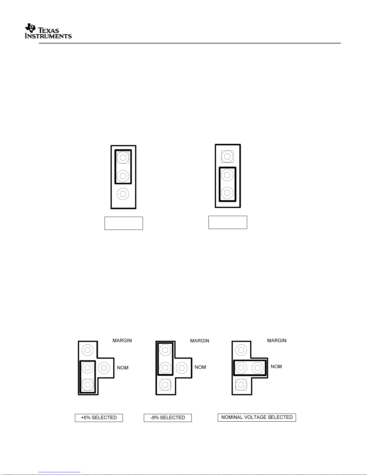
The PTH05010WAS voltage regulators are also equipped with a +/- 5% selectable Margin
Control allowing easy t
esting of the device near the
min/max voltage limits specified in the
datasheet. Place the jumper position to either the “UP 5%”, “DN 5%”, or “NOM” positions
keeping the center pin in common as demonstrated in the following figure.
Figure 4. TLK3134 EVM Regulator Margin Selection
DN
5%
UP
5%
TLK3134 XAUI Transceiver / 4 Channel Multi-Rate Transceiver Evaluation Module (EVM) Users’ Guide 7
DN
UP
5%
5%
DN
UP
5%
5%
Page 8

SLLU104A - September 2007
When the on-board regulators are not being used and independent power supplies are being
used instead, i.e. the case of a voltage tolerance test, the on-board regulators should be disabled
to prevent the regulator’s voltage sense line from trying to regulate the voltage supplied through
the banana jack and not from its own output. This is accomplished by placing a short on the
headers (JMP108, JMP110, and JMP114) labeled “DISABLE”. The remote sense feature is not
designed to compensate for the forward drop of non-linear or frequency dependent components
that may be placed in series with the converter output. Examples include OR-ing diodes, filter
inductors, ferrite beads, and fuses. When these components are enclosed by the remote sense
connection they are effectively placed inside the regulation control loop, which can adversely
affect the stability of the regulator. A large 0 ohm resistor has been installed at the voltage
entrance point of each power plane and can be replaced with a ferrite bead of desired. In this
situation, the 0 ohm resistors on the sense lines can be interchanged to connect the sense line
directly to its output and eliminate the additional components that could otherwise create
instability on the regulator’s output. For the 1.2V regulator, the R223 0 ohm resistor should be
removed and the R222 populated with a 0 ohm resistor. For the 1.5V or 1.8V regulator, R221
should be removed and placed on R220, and similarly R223 should be moved to R222 for the
2.5V regulator.
The VREF plane is sourced through a Voltage Divider providing half of the voltage on the 1P5/8V
plane. The VDDQ and VDDR power
pins of the TLK3134 can both be operated off of either 1.5V
or 1.8V with VREF being half of whatever voltage is on the VDDQ pins. The VREF plane can be
powered through the plane monitoring header (JMP3) and removing the 0 ohm resistor (R71)
although this is not recommended. A separate VDDR plane has been added as there is no
relationship between the VDDR pin and the VDDQ pins, however, the VDDR plane is sourced
through a 0 ohm resistor (R67) from the voltage on the 1P5/8V plane that provides power the
VDDQ pins. This resistor can be replaced with a ferrite bead or removed completely and an
external supply can be connected to the VDDR Header (JMP5) in the case different voltages are
desired on the two planes.
Furthermore, for more accurate current readings the PULLUP_EN Jumpers on all control pin
headers can be removed quickly disconnecting the pullu
p resistors from the voltage plane.
However, the removal of the PULLUP_EN jumpers will also require manual high/low control of
the control pins.
Better Performance can be achieved when the Jitter Cleaner is enabled by using an external
power supply on the 1.2
V Banana Jack. A dedicated LDO 1.2V Regulator powering the Jitter
Cleaner Power Plane should be considered for the end application.
8 TLK3134 XAUI Transceiver / 4 Channel Multi-Rate Transceiver Evaluation Module (EVM) Users’ Guide
Page 9

Power Monitoring LEDs
SLLU104A - September 2007
Each plane of the TLK3134 EVM has been equipped with a Voltage Monitoring circuit that will
monitor the voltage on the plane and light the LEDs when the voltage is within the min/max
datasheet limits for that power supply. A precision TI Voltage Reference chip is used along with
0.1% precision resistors setting min and max reference levels providing a detection circuit that is
accurate to approximately +/- 10mV. The LEDs should be used as a basic indication of the
status of power on the board being within the acceptable min/max limits given in the datasheet,
and not as a precise measurement tool as some LED circuits may turn off at slightly different
voltages when approaching the limits due to the manufacturing tolerances and available
component values.
The voltage monitor circuits can also be bypassed and the LEDs driven directly from the voltage
on the individual planes such as when performing voltage tolerance tests. Inste
only when the voltage on the plane is within the min/max range, the LED will be lit when the
voltage is greater than the voltage needed to turn on the LED drive circuit’s NPN transistor,
allowing current to flow, and the LED to be lit from the 5V source. In the Direct Connect mode,
the base resistors has been given extra margin to allow the LEDs to light when the voltage on
the plane is a little below the minimum limit of that supply in order to provide a LED indicator of
power on the plane during voltage tolerance tests near the lower supply limits.
.
ad of being lit
Figure 5. TLK3134 EVM Voltage Monitor LED Enabled Example
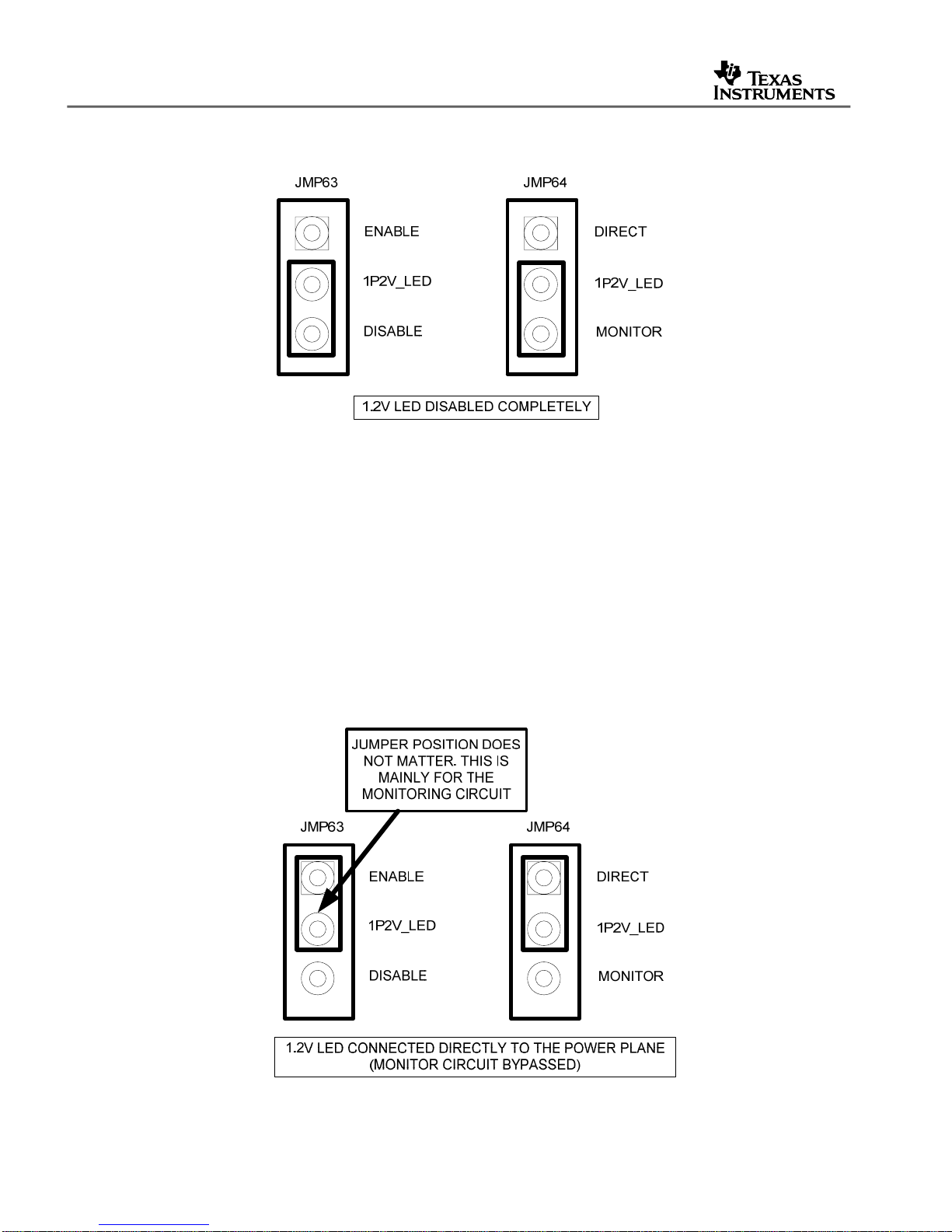
Placing the jumper on the ENABLE side of the Voltage Monitor Enable/Disable header connects
the power plane to the input of the voltage moni
toring circuit. This input is high impedance and
will not load down the power source providing the voltage to the plane.
Placing the header on the MONITOR side of the LED Monitor/Direct Connect selection header
connects the LED drive circui
t to the output of the Voltage Monitor circuit causing the LED to be
lit only when the voltage is within the acceptable range.
TLK3134 XAUI Transceiver / 4 Channel Multi-Rate Transceiver Evaluation Module (EVM) Users’ Guide 9
Page 10
SLLU104A - September 2007
Figure 6. TLK3134 EVM Voltage Monitor LED Disabled Example
Placing the jumper on the DISABLE side of the Voltage Monitor Enable/Disable header
disconnects the power plane to the input of the voltage monitoring cir
cuit and instead ties the
input to GND. This prevents the output of the Voltage Monitoring Circuit from floating and
possibly causing the LED to flicker during contact with the board.
Placing the jumper on the MONITOR side of the LED Monitor/Direct Connect selection header
connects the LED drive circui
t to the output of the Voltage Monitor circuit causing the LED to be
off since the voltage monitor circuit will sense that the plane voltage is GND which is less than
the acceptable plane voltage.
Figure 7. TLK3134 EVM Voltage Monitor LED Connected Directly to Plane Example
10 TLK3134 XAUI Transceiver / 4 Channel Multi-Rate Transceiver Evaluation Module (EVM) Users’ Guide
Page 11

Placing the jumper on the DIRECT side of the LED Monitor/Direct Connect selection header
SLLU104A - September 2007
connects the LED drive circuit to the power plane itself causing the LED to be lit when the
voltage is great enough to cause current to flow through the LED drive circuit. This LED
configuration has been designed to be used when pushing the lower limits of the acceptable
voltage range to continue to provide an indicator that power is on the plane, however without
regards to what that voltage may actually be.
The jumper on the Voltage Monitor Enable/Disable header does not matter as this is only the
input to the voltage monitor circuit which has been bypassed when the LED dri
ve circuit is
connected directly to the power plane itself.
.
TLK3134 XAUI Transceiver / 4 Channel Multi-Rate Transceiver Evaluation Module (EVM) Users’ Guide 11
Page 12
SLLU104A - September 2007
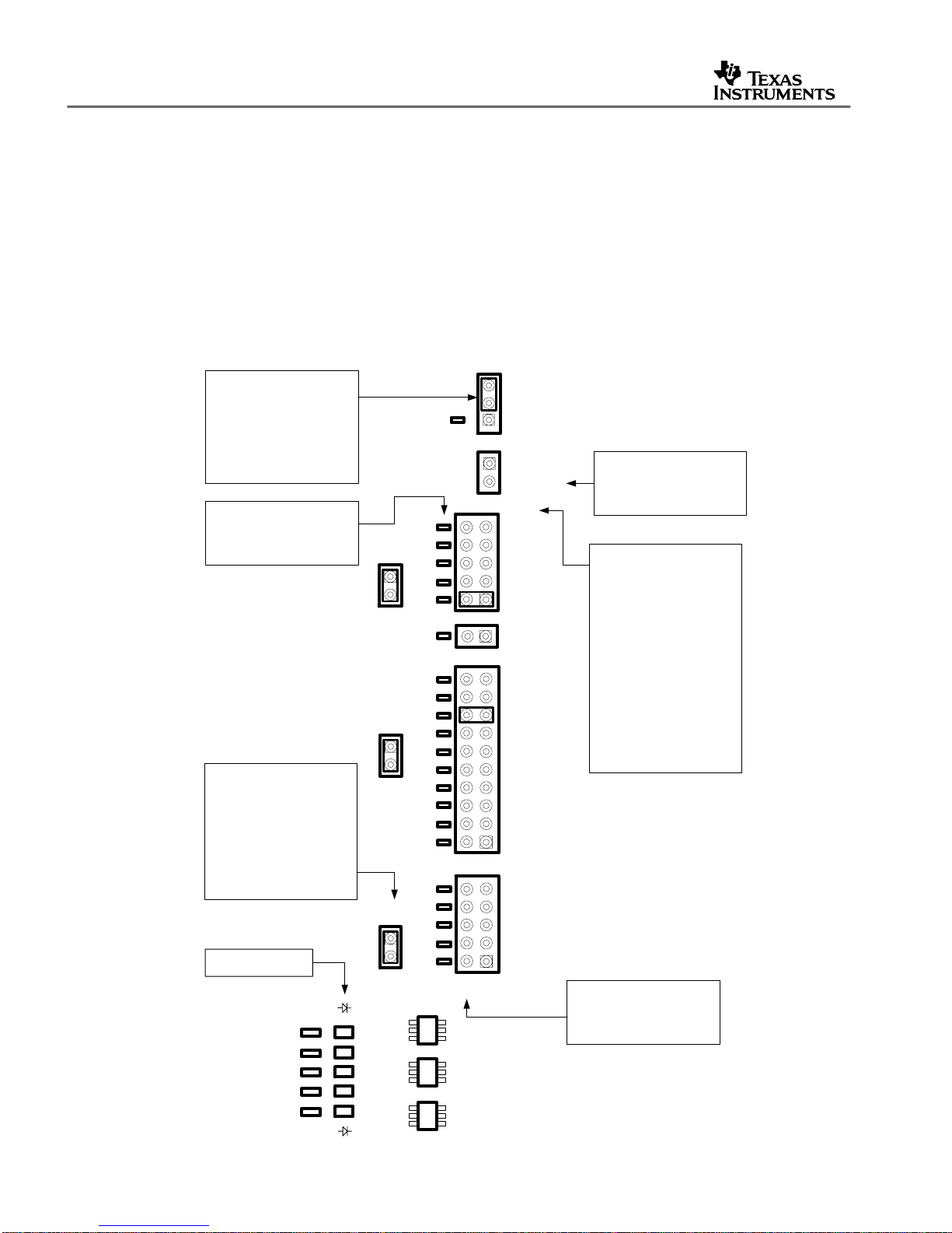
Control Signals
All of the external control pins on the TLK3134 EVM have been consolidated to a single location
on the board and broken out into several header blocks for easier reference. LEDs have been
added to the GPO[4:0] lines in addition to the headers for scope probes, to allow easy monitoring
of the High/Low value on the line. The LED will be ON when the line is a Logic High, and the
LED will be OFF when the line is a Logic Low.
Figure 8. Control Connectors (JMP13, JMP15, JMP20, JMP21, JMP25, JMP26)
THE VCO_TL_TST PIN
GND. A LOCATION FOR
A SERIES INDUCTOR TO
GND HAS BEEN ADDED
HEADER BLOCKS ARE
PULLUP_EN HEADERS
WILL DISCONNECT THE
ACCURATE CURRENT
GPO[4:0] LEDS
SHOULD BE TIED TO
SHOULD IT BECOME
NEEDED.
THE RESISTORS ON
THIS SIDE OF ALL
PULL UP RESISTORS
REMOVING THE
JUMPER ON THE
PULL UP RESISTORS
FROM THE VOLTAGE
PLANE FOR MORE
MEASUREMENTS
R4
R15
R16
R17
R24
PULLUP_EN
PULLUP_EN
PULLUP_EN
D1
GPO0
D2
GPO1
D3
GPO2
D4
GPO3
D5
GPO4
JMP14
JMP12
JMP24
JMP20
GND
JMP21
JMP26
JMP13
GND
VCO_TL_TST
INDUCTOR/GND
GND
TST_OUT
GPO3
GPO2
GPO1
GPO0
GPI1
ST
AMUX0
AMUX1
TESTEN
CODE
PRBS_EN
SLOOP
PLOOP
SPEED0
SPEED1
ENABLE
PRTAD0
PRTAD1
PRTAD2
PRTAD3
PRTAD4
THE PINS ON THIS SIDE
THE TST_OUT PIN
SHOULD BE LEFT OPEN
IN THE APPLICATION
GPO4 HAS NOT BEEN
CONNECTED TO THIS
HEADER BLOCK BUT
RATHER TO A SMP
CONNECTOR LOCATED
ON THE BOTTOM OF
THE BOARD WITH THE
HIGH SPEED LINES.
LEDS HAVE BEEN
CONNECTED TO EACH
OF THE GP0[4:0] PINS
AND ARE LOCATED
BELOW JMP24 AND
JMP25
OF ALL HEADER
BLOCKS ARE GND
L1
JMP15
R39
R38
R37
R36
R35
R55
R14
R13
R12
R11
R10
R9
R8
R7
R6
R5
JMP25
R50
R51
R52
R53
R54
U3
U4
U5
12 TLK3134 XAUI Transceiver / 4 Channel Multi-Rate Transceiver Evaluation Module (EVM) Users’ Guide
Page 13

Control Signal Pin Description:
SLLU104A - September 2007
.
VCO_TL_TST: This pin is the VCO Testability Input and should be grounded in the
application.
TST_OUT: This is the Jitter Cleaner Testability Pin. This signal should be left open
(unconnected) in the System Application.
GPO[4:0]:
These are General Purpose Outputs and must be left open (unconnected) in the
System Application.
GPI1: This is the General Purpose I
ST: This is the MDIO
Select pin and used to select Clause 22 (ST =1) or Clause 45 (ST=0)
nput and must be Grounded in the System Application.
operation.
AMU
X0: This is the SERDES Analog Mux 0 TX pin and must be open (unconnected) in the
System Application.
AMUX1:
This is the SERDES Analog Mux 1 RX pin and must be open (unconnected) in the
System Application.
TESTEN:
This is the Test Mode Enable Input pin and must be Grounded in the System
Application.
CODE
: This is the Code Enable pin. Th
is signal selects different functionality based on the
setting of the ST primary chip input pin.
: This signal is logically OR’d with the XAUI_ORDER register bit (Register
ST=0
Bit 32809.15). XAUI applications can either tie this input signal high (preferred)
or tie this signal low (must program the XAUI_ORDER register bit after device
reset to high if CODE is tied off low). 10GFC applications MUST tie this signal
low.
ST=1
: This signal is logically OR’d with the PCS_EN register bit (Register Bit
17.3). RGMII/GMII applications can either tie this input signal high (preferred) or
tie this signal low (must program the PCS_EN 17.3 register bit after device reset
to high if CODE is tied off low). Nom RGMII/GMII applications MUST tie this
input signal low.
PRBS_EN: This is th
e PRBS Enable Pin. When this pin is asserted HIGH, the internal PRBS
generator and comparator circuits are enabled on the transmit and receive data paths of all
channels. The PRBS results for each channel can be read through MDIO counters. Primary
chip output signals GPO3/GPO2/GPO2/GPO0 remain low during PRBS testing when the input
serial stream PRBS pattern is correct, and pulse high when PRBS errors are detected on the
input serial stream on a per channel basis.
GPO3
GPO2
GPO1
GPO0
: Contains the Channel 3 PRBS currently passing (when low) indication.
: Contains the Channel 2 PRBS currently passing (when low) indication.
: Contains the Channel 1 PRBS currently passing (when low) indication.
: Contains the Channel 0 PRBS currently passing (when low) indication.
An external loopback connection (via external cables) is required during PRBS
testing.
TLK3134 XAUI Transceiver / 4 Channel Multi-Rate Transceiver Evaluation Module (EVM) Users’ Guide 13
Page 14

SLLU104A - September 2007
ST=0: PRBS 223-1 is transmitted on each transmit channel serial output, and
compared on each receive channel serial input.
: PRBS 27-1 is transmitted on each transmit channel serial output, and
ST=1
compared on each receive channel serial input.
SLOOP: This pin is the Serial Loop Enable pin. When SLOOP is asserted HIGH, the serial
input from each channel is internally looped back to that
channel’s serial output, making that
channel a serial repeater. In device configurations where clock tolerance compensation is not
performed in the transmit direction, there are two options for error free serial loopback operation:
1) Frequency lock (0 ppm) the incoming serial data rate to the local reference
clock device
input.
2) Provision the TX SERDES REFCLK to run from
a jitter cleaned version of the
RX SERDES RXBCLK (Receive Byte Clock).
PLOOP: This pin is the Parallel Loop Enable pin. When PLOOP is asserted HIGH, the serial
output for each channel is internally looped back to its serial input so t
hat the transmit parallel
interface input data is output onto the receive parallel interface.
SPEED[1:0]: These are the Speed Selection Pins and put all four channels of the TLK3134 into
one of the three supported (full/half/
quarter) channel operation speeds.
00 – All Four Channels in Full Rate mode
01 – All Four Channels in Half Rate mode
10 – All Four Channels in Quarter Rate mode
11 – Software Selectable Rate
In the Software selectable rate mode, the rate for each channel may be
configured independently by the
The SPEED[1:0] inputs
control both RX and TX directions for all four channels
(Including XAUI and 10GFC
MDIO interface.
modes).
Please see Appendix A of the TLK3134 Datasheet for further information on
speed selection (full/half/quarter) for proper settings as a function
of the
application mode and reference clock frequency.
Please note that if these pins are not configured on the application board to
select “Software Selectable Rate”, then th
cannot be used to control the rate settings, and the full/half/quarter rate
selection is fixed.
ENABLE: This is the Device Enable pin. When ENABLE is held low, the device is in a low
power state. When ENABLE is high the device operates normally. A hard or soft reset muc
be applied after a change of state occurs on this input signal.
14 TLK3134 XAUI Transceiver / 4 Channel Multi-Rate Transceiver Evaluation Module (EVM) Users’ Guide
e internal speed register bits
h
Page 15

PRTAD[4:0]: These are the Port Address Assignment Pins and are used to select the Device
SLLU104A - September 2007
ID/Port ID in Clause 22/Clause 45 MDIO modes.
.
ST=0 (Clause 45 Mode)
:
If PRTAD[0] is a 0, then a PHY device is selected for XAUI/10GFC register
accesses (4.x
xxxx.x).
If PRTAD[0] is a 1, then a DTE device is selected for XAUI/10GFC register
accesses (5.x
xxxx.x).
PRTAD[4:1] selects the Clause 45 port address (TLK3134 must be located on
even boundaries since the lowest port address bit determines DTE/PHY, and is
used as a d
ST=1 (Clause 22 Mode)
evice address instead of port address).
:
PRTAD[4:2] selects a block of four sequential Clause 22 port addresses. Each
channel is implemented as a different port address, and can be accessed by
setting the a
ppropriate port address field within the Clause 22 MDIO transaction.
PRTAD[1:0] pins are not used in Clause 22 mode.
Channel 0 responds to port address 0 within the block of four port addresses.
Channel 1 responds to port address 1 within the block of four port addresses.
Channel 2 responds to port address 2 within the block of four port addresses.
Channel 3 responds to port address 3 within the block of four port addresses.
TLK3134 XAUI Transceiver / 4 Channel Multi-Rate Transceiver Evaluation Module (EVM) Users’ Guide 15
Page 16

SLLU104A - September 2007
MDIO
The TLK3134 supports the Management Data Input/Output (MDIO) Interface as defined in Clauses 22
and 45 of the IEEE 802.3ae Ethernet Specification. The MDIO allows register-based management and
control of the serial links. Normal operation of the TLK3134 is possible without the use of this interface,
however, some additional features are accessible only through this interface.
The MDIO Management Interface consists of a bi-directional data path (MDI
O) and a clock reference
(MDC). The device ID and port address are determined by control pins PRTAD[4:0]. The ST pin
controls whether the device responds as a Clause 22 or Clause 45 device.
In Clause 45 (ST=0), the top 4 control pins PRTAD[4:1] determine the device port address. In Clause
45 mode the TLK3134 can be accessed only through even port addresses. In th
is mode, the TLK3134
will respond if the PHY address field on the MDIO protocol (PA[4:0]) matches {PRTAD[4:1], 1’b0}. The
PRTAD[0] pin acts as a device ID pin where it determines whether the TLK3134 is a DTE or PHY
device and is required to be either 4 (PHY) or 5 (DTE), so only one bit is required to differentiate. If
PRTAD[0] is a 0, then a PHY device is selected for the XGXS. If PRTAD[0] is a 1, then a DTE device is
selected for the XGXS. In this mode, TLK3134 will respond as PHY if the Device address field
(DA[4:0]) on the MDIO protocol is 5’b00100 and as DTE if it is 5’b00101. Note, each register is
accessed as either DTE or PHY devices in the TLK3134, although physically there is only one register
accessed two different ways.
In Clause 22 (ST=1), the top 3 control pins PRTAD[4:2] determine the device port address. In this
mode the 4 individual channels in TLK3134 are classif
ied as 4 different ports. So for any PRTAD[4:2]
value there will be 4 ports per TLK3134. The TLK3134 will respond if the 3 MSB’s of PHY address field
on MDIO protocol (PA[4:2]) matches PRTAD[4:2]. The 2 LSB’s of PHY address field (PA[1:0]) will
determine which channel/port within the TLK3134 to respond.
If PA[1:0] = 2’b00, TLK3134’s Channel 0 will respond.
If PA[1:0] = 2’b01, TLK3134’s Channel 1 will respond.
If PA[1:0] = 2’b10, TLK3134’s Channel 2 will respond.
If PA[1:0] = 2’b11, TLK3134’s Channel 3 will respond.
Write transactions to invalid registers or read only registers will be ignored. Read transactions of invalid
registers will return a “0”.
The bi-directional MDIO pin is pulled up to 1.2V or 2.5V (VDDM) with a 1.5k Ω re
sistor as per the MDI
O
Standard.
Figure 9. TLK3134 EVM MDIO Connector (JMP22)
MDIO
MDC
NC
NC
NC
NC
NC
NC
NC
NC
JMP22
16 TLK3134 XAUI Transceiver / 4 Channel Multi-Rate Transceiver Evaluation Module (EVM) Users’ Guide
GND
GND
NC
NC
NC
NC
NC
NC
NC
NC
Page 17
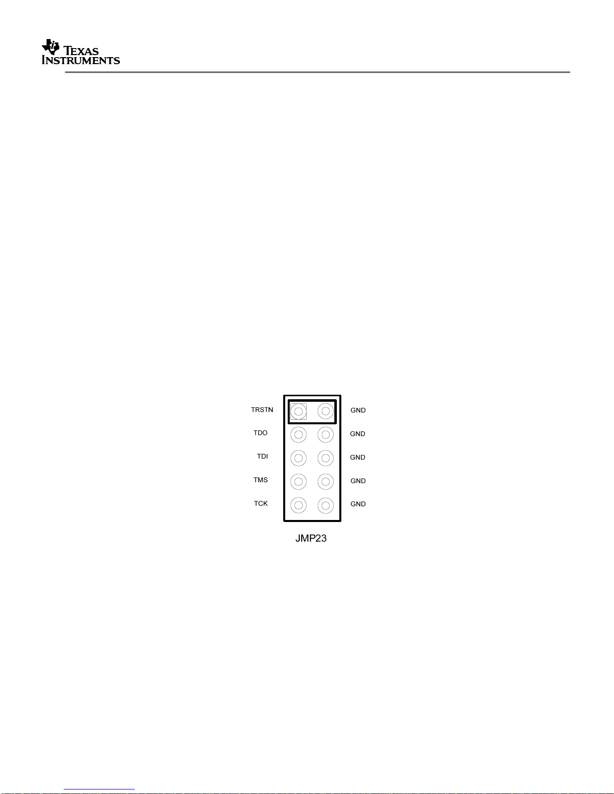
JTAG
SLLU104A - September 2007
The EVM also provides a separate connector to support the full five-pin JTAG interface of the TLK3134
as defined in IEEE 1149.1 for manufacturing tests.
.
TDI: This pin is the JTAG Input Data pin and is used
to serially shift test data and test
instructions into the device during the operation of the test port.
TDO: This pin is the JTAG Outp
ut Data pin and is used to serially shift test data and test
instructions out of the device during operation of the test port. When JTAG port is not in use,
TDO is in a high impedance state.
TMS: This pin is the JTAG Mode Select pin and is used to control the state of the internal testport controller.
TCK: This is the JTAG Clock pin and is used to clock stat
e information and test data into and
out of the device during the operation of the test port.
TRST_N: This is the JTAG Test Reset pin and is used to reset the JTAG logic into system
operational mode. NOTE
: TRST_N should be tied low when the JTAG port is not in use and
during normal operation of the port as shown in the following figure.
Figure 10. TLK3134 EVM JTAG Connector (JMP23)
TLK3134 XAUI Transceiver / 4 Channel Multi-Rate Transceiver Evaluation Module (EVM) Users’ Guide 17
Page 18
SLLU104A - September 2007
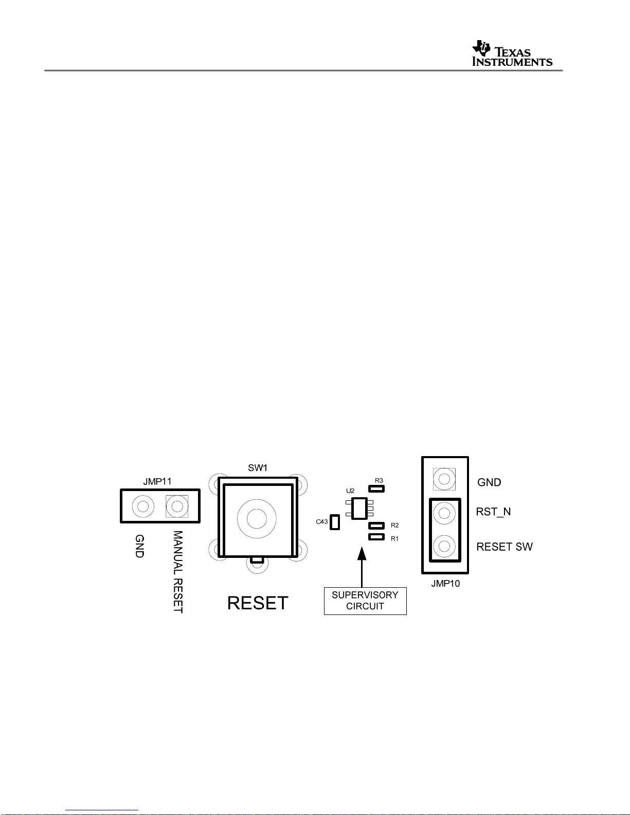
Reset
The TLK3134 EVM comes configured for Manual Reset operations involving the Pushbutton
Reset Switch (SW1). When switch SW1 is pressed, the TLK3134 device RESET pin (RST_N)
goes LOW and the entire TLK3134 device is reinitialized. A TI TPS3125J18 Ultra Low Voltage
Processor Supervisory Circuit is used to control the Reset line. During power-on, /RESET pin of
U2 is asserted when the supply voltage becomes higher than 0.75V. Thereafter, the supply
voltage supervisor monitors the voltage and keeps /RESET output active as long as the Voltage
remains below the threshold voltage (V
inactive state (high) to ensure proper system reset. The delay time, t
voltage has risen above the threshold voltage (V
There is also a manual reset input to the supervisory circuit, /MR, which accepts the input from
the pushbutton switch SW
the TLK3134 device whenever the pushbutton RESET is pressed. By placing a jumper on
JMP11, the Manual Reset (/MR) is tied hard to ground causing the TLK3134 to be held in a
constant state of Reset without the need to continually hold the Reset Pushbutton SW1. The
Supervisory circuit will release the Reset line to a HIGH 180mS (t
becomes greater than the threshold voltage (V
By removing the jumper from JMP10, the Supervised Reset Circuit is disconnected from the
RST_N line. Reset control from an external controller or piec
directly to pin 2 (RST_N) of JMP10 and a ground pin GND has been added to the JMP10 header
next to the RST_N pin to allow easy access for the return current on that cable.
). An internal timer delays the return of the output to the
IT
=180ms, starts after the
d
).
IT
1. A low level at /MR causes /RESET to become active, thus resetting
) from the time the /MR line
d
).
IT
e of equipment can be connected
Figure 11. RESET Switch (SW1, JMP10, or JMP11)
NOTE: The Jumper on JMP10 connecting RESET SW to RST_N must be connected as shown
in order to cause the TLK3134 to be reset and reinitialized If switch
SW1 is pressed, the device
RESET pin (RST_N) goes LOW, the entire TLK3134 device is reinitialized.
18 TLK3134 XAUI Transceiver / 4 Channel Multi-Rate Transceiver Evaluation Module (EVM) Users’ Guide
Page 19
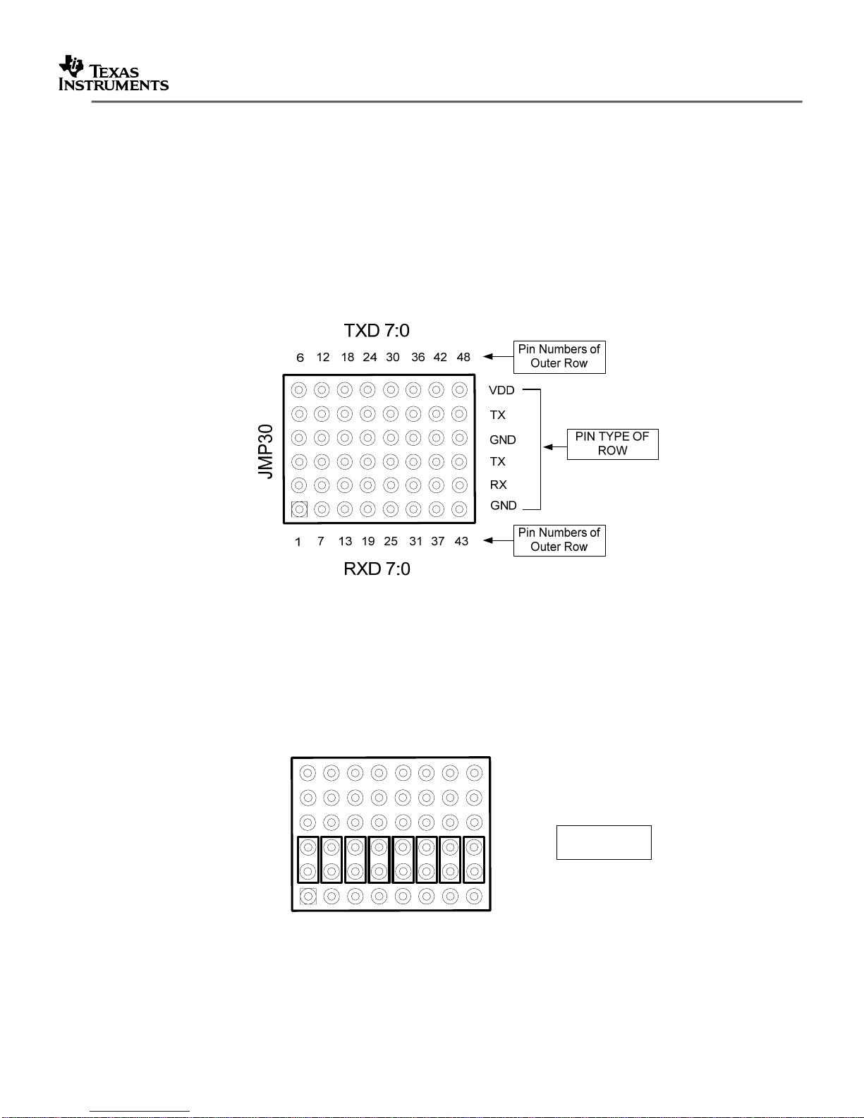
Parallel Signals
SLLU104A - September 2007
The parallel signals have on the TLK3134 EVM have been routed to a 0.1” header block that is
configured like the following figure. All RXD pins on all 4 header blocks (RXD[7:0], RXD[15:8],
RXD[23:16], RXD[31:24]), as well as all TXD pins on all 4 header blocks (TXD[7:0], TXD[15:8],
TXD[23:16], TXD[31:24]), have matched trace lengths to themselves +/- 1MIL. Due to routing
constraints RXD[31:0] and TXD[31:0] trace lengths are not matched to each other, but only to
themselves.
.
Figure 12. Parallel Signal Header Block Example
Parallel Loop back, shown in the following figure, can be easily implemented by placing Jumper
s
on the RX/TX pins of the header. For example, placing a jumper on pins 2 and 3 of JMP30 will
loop back TXD7 to RXD7.
Figure 13. Parallel Signal Header Block Example
TXD 7:0
JMP30
12
6
7
1
RXD 7:0
484218 24 30 36
VDD
TX
GND
TX
RX
GND
433713 19 25 31
PARALLEL
LOOPBACK
TLK3134 XAUI Transceiver / 4 Channel Multi-Rate Transceiver Evaluation Module (EVM) Users’ Guide 19
Page 20

SLLU104A - September 2007
Additional GND and VDD pins have been added into the header block for several reasons. The
GND pins next to the RXD and TXD pins provide a convenient ground reference for a scope
probe or coax cables. The additional TXD row and VDD pins allow a static pattern to be driven
into the TXD bus by placing jumpers across either the TXD and VDD pins for a HIGH, or TXD
and GND pins for a LOW eliminating the need for cables during quick tests. The extra row of
TXD can also be used to monitor the signals on the TXD pins while simultaneously looping back
into the RXD pins. The following figure shows a clock pattern (01010101) on TXD[7:0] being
looped back onto the RXD[7:0] pins.
Figure 14. Parallel Loop Back with Static Data Pattern Example
TXD 7:0
12
6
JMP30
7
1
RXD 7:0
484218 24 30 36
VDD
TX
GND
TX
RX
GND
433713 19 25 31
PARALLEL
LOOPBACK
The Transmit Data Clocks and Receive Data Clocks (XGMII) are located in header blocks
JMP32 and JMP33 with the clock pins next to
each other. These four signals are the parallel
(XGMII) side input and output clocks per channel. In XAUI/10GFC mode, TXCLK_1 and
RXCLK_1 are used. During Parallel Loopback, the clocks can be jumpered together as shown in
the following diagram.
Figure 15. Parallel Loop Back with Static Data Pattern Example
20 TLK3134 XAUI Transceiver / 4 Channel Multi-Rate Transceiver Evaluation Module (EVM) Users’ Guide
Page 21

XAUI Mode (XGMII) Test and Setup Configuration
SLLU104A - September 2007
The device reset requirements and setup procedure to configure the TLK3134 for XAUII Mode
(XGMII) is as follows:
REFCLK frequency = 156.25 MHz, Serdes Data Rate = Full Rate, Mode = Transceiver,
Edge Mode = Source Centered, RX_CLK out = TXBCLK, Jitter Cleaner PLL Multiplier Ratio = 1X or Off
• Device Pin Setting(s) – Pin settings allow for maximum software configurability.
Ensure ST input pin is Low.
o
o Ensure CODE input pin is Low.
o Ensure PLOOP input pin is Low.
o Ensure SLOOP input pin is Low.
o Ensure SPEED [1:0] input pins are both High.
o Ensure ENABLE input pin is High.
o Ensure PRBS_EN input pin is Low.
• Reset Device
Issue a hard or soft reset (RST_N asserted for at least 10 us -or- Write 1’b1 to 4/5.0.15)
o
• Clock Configuration
If using JCPLL (JCPLL 1X)
o
JCPLL Mux Settings (Figure 3
Select REFCLK input (Default = Differential)
• If Single Ended REFCLK used – Write 2’b01 to 4/5.37120.15:14
• If Differential REFCLK used – Write 2’b00 to 4/5.37120.15:14
Write 2’b11 to 4/5.37120.13:12 to select differential REFCLKP/N as RXBYTECLK
Write 4’b0000 to 4/5.37120.11:8 to select jitter clean
Write 2’b00 to 4/5.37120.5:4 to select jitter clean
Write 2’b00 to 4/5.32810.15:14 to select SERDES TX clock as RX_CLK output
Write 16’h0081 to 4/5.37126 to set Charge pump control
Write 16’h0080 to 4/5.37128 to set TXRX output divider
Clock Divid
If using clock bypass mode (JCPLL Off)
o
JCPLL Mux Settings (Figure 3
TLK3134 XAUI Transceiver / 4 Channel Multi-Rate Transceiver Evaluation Module (EVM) Users’ Guide 21
e Settings (Table 211
Write 7’b1000000 to 4/5.37124.14:8 to set REF_DIV to value of 1
Write 1’b1 to 4/5.37124.15 REFDIV_EN to enable reference clock divider
Write 7’h14 to 4/5.37124.6:0 to set FB
Write 1’b1 to 4/5.37124.7 FBDIV_EN to enable feedback divider
Write 7’h14 to 4/5.37125.6:0 to set RXTX_DIV to value of 20
Write 1’b1 to 4/5.37125.7 OUTDIV_EN to enable output divider
Write 7’h0D to 4/5.37121.14:8 to set HSTL_DIV to value of 13
Write 7’h06 to 4/5.37121.6:0 to set HSTL_DIV2 to value
Write 15’h1515 to 4/5.36864.14:0 SERDES_PLL_CONFIG to set MPY RX/T
Write 16’h0000 to 4/5.36865 SERDES_RATE_CONFIG_TX_RX to set Full Rate
Write 1’b1 to 4/5.37127.15 to enable Jitter Cleaner
Wait 2 ms in order for JCPLL to lock
Select REFCLK input (Default = Differential)
• If Single Ended REFCLK used – Write 2’b01 to 4/5.37120.15:14
• If Differential REFCLK used – Write 2’b00 to 4/5.37120.15:14
Select RXBYTE_CLK (Default = Differential)
• If Single Ended REFCLK used – Write 2’b10 to 4/5.37120.13:12
• If Differential REFCLK used – Write 2’b11 to 4/5.37120.13:12
Select SERDES TX Reference Clock Input (Default = Differential)
• If Single Ended REFCLK used – Write 2’b10 to 4/5.37120.11:10
• If Differential REFCLK used – Write 2’b11 to 4/5.37120.11:10
Select SERDES RX Reference Clock Input (Default = Differential)
• If Single Ended REFCLK used – Write 2’b10 to 4/5.37120.9:8
• If Differential REFCLK used – W
Select HSTL_2X_CLK (Default = Differential)
• If Single Ended REFCLK used – Write 2’b10 to 4/5.37120.5:4
• If Differential REFCLK used – W
of the TLK3134 Datasheet)
of the TLK3134 Datasheet)
_DIV to value of 20
of the TLK3134 Datasheet)
ite 2’b11 to 4/5.37120.9:8
r
ite 2’b11 to 4/5.37120.5:4
r
ed clock
ed clock for HSTL VTP 2x
for SERDES TX/RX.
of 6
.
X multiplier factor to 10
Page 22

SLLU104A - September 2007
Write 2’b00 to 4/5.32810.15:14 to select SERDES TX clock as RX_CLK output
Write 6’h04 to 4/5.37121.6:0 to set HSTL_DIV2 to value of 4.
Write 16’h0000 to 4/5.36865 SERDES_RATE_CONFIG_TX_RX to set Full Rate
• Mode Control (Table 2
o Write 1’b1 to 4/5.32809.15
o Write 1’b0 to 4/5.32808.15 to set source centered data for TX side
o Write 1’b0 to 4/5.32808.11 to set source centered data for RX side
o Write 1’b0 to 4/5.32792.1 to disable XAUI data loop back
o Write 1’b0 to 4/5.32792.0 to disable XGMII data loop back
o Write 1’b0 to 4/5.0.14 to disable loop back mode
o Write 3’b110 to 4/5.36874.11:9 to set lane 0 TX swing setting amplitude to 1250 mVdfpp
o Write 3’b110 to 4/5.36876.11:9 to set lane 1 TX
o Write 3’b110 to 4/5.36878.11:9 to set lane 2 TX
o Write 3’b110 to 4/5.36880.11:9 to set lane 3 TX
• Poll Serdes PLL Status for Locked State
o Read 4/5.36891.4,0 SERDES_PLL_STAT
o Keep polling until both bits are high.
•
Issue Data path Reset
Write 1’b1 to 4/5.32800.15
o
• Clear Latched Registers
o
Read 4/5.1 XS_STATUS_1 to clear
o Read 4/5.8 XS_STATUS_2 to clear
o Read 4/5.32770 TX_FIFO_STATUS to clear
o Read 4/5.32771 TX_FIFO_DROP_COUNT to clear
o Read 4/5.32772 TX_FIFO_INSERT_COUNT to clear
o Read 4/5.32773 TX_CODEGEN_STATUS to clear
o Read 4/5.(32780,1,2,3) LANE_0~3_EOP_E
o Read 4/5.(32784,5,6,7) LANE_0~3_CODE_ERROR
o Read 4/5.32789 RX_LANE_ALIGN_STATUS to clear
o Read 4/5.32790 RX_CHANNEL_SYNC_STATUS to clear
o Read 4/5.32794 RX_CTC_STATUS to clear
o Read 4/5.32795 RX_CTC_INSERT_COUNT to clear
o Read 4/5.32796 RX_CTC_DELETE_COUNT to clear
o Read 4/5.32797 DATA_DOWN to clear
o Read 4/5.32799 CLOCK_DOWN_STATUS to clear
o Read 4/5.36891 SERDES_PLL_STATUS to clear
• Operational Mode Status
o Read Verify 4/5.1.7 XS_STATUS_1 – Fault (1’b0)
o Read Verify 4/5.1.2 XS_STATUS_1 – XS Transmit Link Status (1’b1)
o Read Verify 4/5.8.11 XS_STATUS_2 – Transmit fault (1’b0)
o Read Verify 4/5.8.10 XS_STATUS_2 – Receive fault (1’b0)
o Read Verify 4/5.24.12 XS_LANE_STAT
o Read Verify 4/5.24.3:0 XS_LANE_STAT
o Read Verify 4/5.32773.6:0 TX_CODEGEN_STATUS (6’b000000)
o Read Verify 4/5.36891.4 SERDES_PLL_STATUS – PLL_LOCK_RX (1’b1)
o Read Verify 4/5.36891.0 SERDES_PLL_STATUS – PLL_LOCK_TX (1’b1)
of the TLK3134 Datasheet)
XAUI_ORDER
swing setting amplitude to 1250 mVdfpp
swing setting amplitude to 1250 mVdfpp
swing setting amplitude to 1250 mVdfpp
US – PLL_LOCK_TX/RX
RROR_COUNT to clear
_COUNT to clear
US – Align status (1’b1)
US – Lane (3-0) sync (4’b1111)
22 TLK3134 XAUI Transceiver / 4 Channel Multi-Rate Transceiver Evaluation Module (EVM) Users’ Guide
Page 23

Figure 16. Example TLK3134 EVM Test Configuration – XAUI Mode (XGMII) Parallel Loopback
SLLU104A - September 2007
D
D
8
4
V
4
2
X
2
:
4
T
D
1
6
N
3
3
G
0
D
X
T
1
2
1
6
7
X
3
T
X
4
2
8
2
P
M
J
D
R
N
G
3
4
7
3
1
3
4
5
2
2
:
9
1
1
3
3
D
1
X
7
R
1
V
D
D
T
6
G
X
1
T
N
2
X
D
1
T
R
G
X
N
D
1
7
R
D
8
X
1
X
7
2
:
4
0
3
0
3
6
4
2
4
3
1
9
2
5
D
7
:
0
8
0
3
P
3
1
M
3
J
7
4
3
.
TLK3134 XAUI Transceiver / 4 Channel Multi-Rate Transceiver Evaluation Module (EVM) Users’ Guide 23
Page 24

SLLU104A - September 2007
Gigabit Ethernet Mode (RGMII) Test and Setup Configuration
The device reset requirements and setup procedure to configure the TLK3134 for Gigabit
Ethernet Mode (RGMII) is as follows:
*Note: All global registers must be accessed indirectly through Clause 22.
REFCLK frequency = 125 MHz, Serdes Data Rate = Half Rate, Mode = Tr
RX_CLK[n] out = TXBCLK[n], Jitter Cleaner PLL Multiplier Ratio = 1X or Off
• Device Pin Setting(s) – Pin settings allow for maximum software configurability.
o Ensure ST input pin is high.
o Ensure CODE input pin is Low.
o Ensure PLOOP input pin is Low.
o Ensure SLOOP input pin is Low.
o Ensure SPEED [1:0] input pins are both High.
o Ensure ENABLE input pin is High.
o Ensure PRBS_EN input pin is Low.
• Reset Device
Issue a hard or soft reset (RST_N asserted for at least 10 us -or- W
o
• Clock Configuration
o If using JCPLL (JCPLL 1X)
JCPLL Mux Settings (
Select REFCLK input (Default = Differential)
• If Single Ended REFCLK used – Write 2’b01 to 4/5.37120.15:14
• If Differential REFCLK used – Write 2’b00 to 4/5.37120.15:14
Write 2’b11 to 4/5.37120.13:12 to select differential REFCLKP/N as RXBYTECLK
Write 4’b0000 to 4/5.37120.11:8 to select jitter cleaned clock
Write 2’b11 to 4/5.37120.7:6 to select differential REFC
Write 2’b00 to 4/5.37120.5:4 to select jitter clean
Write 2’b00 to 16.10:9 to select SERDES TX clock as RX_CLK output (per channel)
Write 16’h0081 to 4/5.37126 to set Charge pump control
Write 16’h0080 to 4/5.37128 to set TXRX output divider
Clock Divid
Write 7’b1000000 to 4/5.37124.14:8 to set REF_DIV to value of 1
Write 1’b1 to 4/5.37124.15 REFDIV_EN to enable reference clock divider
Write 7’h18 to 4/5.37124.6:0 to set FB_DIV to value of 24
Write 1’b1 to 4/5.37124.7 FBDIV_EN to enable feedback divider
Write 7’h18 to 4/5.37125.6:0 to set RXTX_DIV to value of 24
Write 1’b1 to 4/5.37125.7 OUTDIV_EN to enable RXTX_DIV output divider
Write 7’h0D to 4/5.37121.14:8 to set HSTL_DIV to value of 13
Write 7’h06 to 4/5.37121.6:0 to set HSTL_DIV2 to value
Write 15’h1515 to 4/5.36864.14:0 SERDES_PLL_CONFIG to set MPY RX/T
Write 16’h5555 to 4/5.36865 SERDES_RATE_CONFIG_TX_RX to set Half Rate
Write 1’b1 to 4/5.37127.15 to enable Jitter Cleaner
Wait 2 ms in order for JCPLL to lock
Else if using clock bypass mode (JCPLL Off)
o
JCPLL Mux Settings (
Select REFCLK input (Default = Differential)
• If Single Ended REFCLK used – Write 2’b01 to 4/5.37120.15:14
• If Differential REFCLK used – Write 2’b00 to 4/5.37120.15:14
Select RXBYTE_CLK (Default = Differential)
• If Single Ended REFCLK used – Write 2’b10 to 4/5.37120.13:12
• If Differential REFCLK used – Write 2’b11 to 4/5.37120.13:12
Select SERDES TX Reference Clock Input (Default = Differential)
• If Single Ended REFCLK used – Write 2’b10 to 4/5.37120.11:10
Figure 3 of the TLK3134 Datasheet)
e Settings (Table 211 of the TLK3134 Datasheet)
Figure 3 of the TLK3134 Datasheet)
• If Differential REFCLK used – Write 2’b11 to 4/5.37120.11:10
Select SERDES RX Reference Clock Input (Default = Differential)
ansceiver, Edge Mode = Source Centered Mode,
rite 1’b1 to 0.15)
for SERDES TX/RX.
LKP/N as Delay Stopwatch clock input
ed clock for HSTL VTP 2x
of 6
X multiplier factor to 10
24 TLK3134 XAUI Transceiver / 4 Channel Multi-Rate Transceiver Evaluation Module (EVM) Users’ Guide
Page 25

• If Single Ended REFCLK used – Write 2’b10 to 4/5.37120.9:8
SLLU104A - September 2007
• If Differential REFCLK used – Write 2’b11 to 4/5.37120.9:8
Select DELAY_CLK (Default = Differential)
• If Single Ended REFCLK used – Write 2’b10 to 4/5.37120.7:6
• If Differential REFCLK used – Write 2’b11 to 4/5.37120.7:6
Select HSTL_2X_CLK (Default = Differential)
• If Single Ended REFCLK used – Write 2’b10 to 4/5.37120.5:4
• If Differential REFCLK used – W
Write 2’b00 to 16.10:9 to select SERDES TX clock as RX_CLK output (per channel)
Write 6’h04 to 4/5.37121.6:0 to set HSTL_DIV2 to value of 4.
Write 15’h1515 to 4/5.36864.14:0 SERDES_PLL_CONFIG to set MPY RX/T
Write 16’h5555 to 4/5.36865 SERDES_RATE_CONFIG_TX_RX to set Half Rate
• Mode Control (Table 2
o Write 1’b0 to 17.0 for RX source centered mode (per channel)
o Write 1’b0 to 17.1 for TX source centered mode (per channel)
o Write 1’b1 to 17.2 to enable 8B/10B encode decode functions (per channel)
o Write 1’b1 to 17.3 to enable 1000Base-X PCS TX & PCS RX functions (per channel)
o Write 1’b1 to 17.4 to set nibble order, LSB on rising edge, MSB on falling edge (per channel)
o Write 1’b1 to 17.5 to enable DDR data on TX/RX directions (per channel)
o Write 1’b0 to 17.6 to disable FC_PH overlay detection (per channel)
o Write 1’b1 to 17.7 to enable comma detection (per channel)
o Write 1’b0 to 17.9 to disable full DDR mode (per channel)
o Write 1’b0 to 16.8 to disable Farend Loop back (per channel)
o Write 1’b0 to 0.14 to disable loop back mode (per channel)
o Write 3’b111 to 4/5.36874.11:9 to set channel 0 TX swing setting amplitude to 1375 mVdfpp
o Write 3’b111 to 4/5.36876.11:9 to set channel 1 TX s
o Write 3’b111 to 4/5.36878.11:9 to set channel 2 TX s
o Write 3’b111 to 4/5.36880.11:9 to set channel 3 TX s
• Poll Serdes PLL Status for Locked State
o
Read 4/5.36891.4,0 SERDES_PLL_STAT
o Keep polling until both bits are high.
• Issue Data path Reset
Write 1’b1 to 16.11 (per channel)
o
• Clear Latched Registers
Read 1 PHY_STATUS_1 to clear (per channel)
o
o Read 18 PHY_RX_CTC_FIFO_STATUS to clear (per channel)
o Read 19 PHY_TX_CTC_FIFO_STATUS to clear (per channel)
o Read 28 PHY_CHANNEL_STATUS to clear (per channel)
o Read 4/5.36891 SERDES_PLL_STATUS to clear
• Operational Mode Status
o
Read Verify 1.2 PHY_STATUS_1 – Link Status (1’b1) (per channel)
o Read Verify 18.15 PHY_RX_CTC_FIFO_STATUS – RX_CTC_Reset (1’b0) (per channel)
o Read Verify 19.15 PHY_TX_CTC_FIFO_STATUS – TX_FIFO_Reset_1Gx (1’b0) (per channel)
o Read Verify 28.13:12 PHY_CHANNEL_STATUS – Enc/Dec Invalid Code Word (2’b00) (per channel)
o Read Verify 4/5.36891.4 SERDES_PLL_STATUS – PLL_LOCK_RX (1’b1)
of the TLK3134 Datasheet)
o Read Verify 4/5.36891.0 SERDES_PLL_STATUS – PLL_LOCK_TX (1’b1)
ite 2’b11 to 4/5.37120.5:4
r
wing setting amplitude to 1375 mVdfpp
wing setting amplitude to 1375 mVdfpp
wing setting amplitude to 1375 mVdfpp
US – PLL_LOCK_TX/RX
.
X multiplier factor to 10
TLK3134 XAUI Transceiver / 4 Channel Multi-Rate Transceiver Evaluation Module (EVM) Users’ Guide 25
Page 26

SLLU104A - September 2007
Figure 17. Example TLK3134 EVM Test Configuration – Gigabit Ethernet Mode (RGMII) Serial Loopback
D
D
84
V
4
2
TX
D
6
N
31:24
3
G
TX
TXD
182430
12
6
X
D
R
N
G
43
71
3
31
4
5
2
2
:
9
1
1
3
3
D
JMP27
X
7
R
1
V
D
D
TX
6
G
1
TXD 7:0
N
2
D
TX
R
GND
X
1
7
131925
R
X
D 7:0
4
2182430 36
48
0
3
3
1
JMP
7
4
33
4
O
P
G
P
K
N
T
L
K
D
C
L
C
F
E
R
N
F
R
E
0
E
R
FC
T
DN1
LK
T
D
P
0
3
P
D
R
2
P
D
2
R
1
N
P
D
D
R
R
1
N
D
R
26 TLK3134 XAUI Transceiver / 4 Channel Multi-Rate Transceiver Evaluation Module (EVM) Users’ Guide
Page 27

Schematics
SLLU104A - September 2007
.
Figure 18. TLK3134 EVM Schematic, Sheet 1 Index
TLK3134 XAUI Transceiver / 4 Channel Multi-Rate Transceiver Evaluation Module (EVM) Users’ Guide 27
Page 28

SLLU104A - September 2007
Figure 19. TLK3134 EVM Schematic, Sheet 2 Device Power and Ground
28 TLK3134 XAUI Transceiver / 4 Channel Multi-Rate Transceiver Evaluation Module (EVM) Users’ Guide
Page 29

Figure 20. TLK3134 EVM Schematic, Sheet 3 Global Signals
SLLU104A - September 2007
.
TLK3134 XAUI Transceiver / 4 Channel Multi-Rate Transceiver Evaluation Module (EVM) Users’ Guide 29
Page 30

SLLU104A - September 2007
Figure 21. TLK3134 EVM Schematic, Sheet 4 High Speed Differential
30 TLK3134 XAUI Transceiver / 4 Channel Multi-Rate Transceiver Evaluation Module (EVM) Users’ Guide
Page 31

Figure 22. TLK3134 EVM Schematic, Sheet 5 Jitter Cleaner Clock
SLLU104A - September 2007
.
TLK3134 XAUI Transceiver / 4 Channel Multi-Rate Transceiver Evaluation Module (EVM) Users’ Guide 31
Page 32

SLLU104A - September 2007
Figure 23. TLK3134 EVM Schematic, Sheet 6 JTAG and MDIO
of
616
REV PAGEDOCUMENT NUMBERSIZE
1
1
TEXAS INSTURMENTS
6493231
2 Pin Berg Jumper
JMP24
1
MDIO KEYED CONNECTOR
PRTAD4
PRTAD3
PRTAD2
PRTAD4N5PRTAD3N4PRTAD2N3PRTAD1N2PRTAD0
2
2P5V
PRTAD_PULLUP_EN
PRTAD1
PRTAD0
M5
T1
M2
ST
REFCLK
JMP22
1 2
3 4
5 6
7 8
9 10
11 12
13 14
15 16
17 18
19 20
C94
NP
MDIO_CON
MDC_CON
C93
NP
2
R45 0
R46 0
R48
NP
R44
NP
R47
VDDM
R43
1.5K
3
NP
MDC
MDIO
U16
T16
MDC
MDIO
U1C
246810
JMP25
Header 5x2
13579
R54 4.99K
R53 4.99K
R52 4.99K
R51 4.99K
R50 4.99K
2P5V
R49
49.9
TLK3134
NOTE: PLACE THIS
TERMINATION RESISTOR
AS CLOSE TO THE
DEVICE PIN AS
POSSIBLE.
1
2
JMP26
R55 4.99K
ST
J20
REFCLK
2 Pin Berg Jumper
REFCLK
B
JTAG AND MDIO
PAGE TITLE
2
3
4
5
D D
32 TLK3134 XAUI Transceiver / 4 Channel Multi-Rate Transceiver Evaluation Module (EVM) Users’ Guide
246810
13579
TDI
TRST_N
TDO
N13
R15
N15
TDO
TRST_N
Header 5x2
TCK
TMS
P15
P17
TDI
TMS
TCK
TLK3134
B B
A A
4
5
JMP23
U1B
C C
Page 33

Figure 24. TLK3134 EVM Schematic, Sheet 7 TX and RX Data Lines
SLLU104A - September 2007
47
47
48
41
42
35
36
29
30
23
24
17
18
11
12
5
6
47
48
41
42
35
36
29
30
23
24
17
18
11
12
5
6
48
41
42
35
36
29
30
23
24
17
18
11
12
5
6
47
48
41
42
35
36
29
30
23
24
17
18
11
12
5
6
.
TLK3134 XAUI Transceiver / 4 Channel Multi-Rate Transceiver Evaluation Module (EVM) Users’ Guide 33
Page 34

SLLU104A - September 2007
Figure 25. TLK3134 EVM Schematic, Sheet 8 TX/RX Clocks and Control
34 TLK3134 XAUI Transceiver / 4 Channel Multi-Rate Transceiver Evaluation Module (EVM) Users’ Guide
Page 35

Figure 26. TLK3134 EVM Schematic, Sheet 9 Power Regulation
SLLU104A - September 2007
3
2
1P8V_VADJ
1
1P5V_VADJ
.
12
12
12
12
12
C99 .01uf
C98 0.1uf
C97 1.0uf
C96 10uf
C95 68uf
12
12
12
12
12
12
12
12
12
12
TLK3134 XAUI Transceiver / 4 Channel Multi-Rate Transceiver Evaluation Module (EVM) Users’ Guide 35
Page 36

SLLU104A - September 2007
Figure 27. TLK3134 EVM Schematic, Sheet 10 Power Distribution
C142 .01uf
C141 0.1uf
C140 1.0uf
C170 0.1uf
C169 1.0uf
C173 10uf
C167 .01uf
C166 0.1uf
C165 1.0uf
R73 100
C181 .01uf
C180 0.1uf
C179 1.0uf
C183 10uf
C182 68uf
C176 .01uf
C178 0.1uf
C177 100uf
C168 .01uf
C175 0.1uf
C174 1.0uf
C186 .01uf C171 .01uf
C185 0.1uf
C184 1.0uf
C188 10uf
C187 68uf C172 68uf
1
36 TLK3134 XAUI Transceiver / 4 Channel Multi-Rate Transceiver Evaluation Module (EVM) Users’ Guide
1
1
Page 37

Figure 28. TLK3134 EVM Schematic, Sheet 11 1P2V and 2P5V Supply LEDs
SLLU104A - September 2007
.
TLK3134 XAUI Transceiver / 4 Channel Multi-Rate Transceiver Evaluation Module (EVM) Users’ Guide 37
Page 38

SLLU104A - September 2007
Figure 29. TLK3134 EVM Schematic, Sheet 12 1P5V, 1P8V, and 5V Supply LEDs
of
12 16
REV PAGEDOCUMENT NUMBERSIZE
1
2
3
R94 49 .9
5V 5V
R93 49 .9
5V
1P5V_LED_WINDOW_OUT
R96
105K
1
1 OUT
LM339AU14B
-
+
1 IN_P71 IN_N
6
1P8V_LED_VF
1P5V_LED_VF
LM339AU14C
21
21
2
2 OUT
-
+
2 IN_N42 IN_P
5
D9
D8
HSMB-C170
HSMB-C170
1P5V_LED_COL
C11E12C2
U16
JMP68
TEXAS INSTURMENTS
1P8V_LED_COL
3
5
E2
B2
B1
6
1P5V_LED_BASE
LED SELECT
123
JMP69
1P5V_LED_PLANE_OUT
R99 18.7K
R100 26.7K
1P5/8V
1P5/8V
123
1P8V_LED_PLANE_OUT
4
1P8V_LED_BASE
ZXTD09N50DE6
LED SELECT
5V
1P8V_LED_WINDOW_OUT
R102
105K
14
LM339AU14D
+
9
13
3 OUT
4 OUT
LM339AU14E
-
3 IN_N83 IN_P
+
4 IN_P114 IN_N
-
10
12
GND
LM339AU14A
VCC
3
5V
1
6493231
B
1P5V, 1P8V, AND 5V SUPPLY LEDS
PAGE TITLE
2
3
4
4P096V_REF2
5
NOTE: VOLTAGE WINDOW DETECTOR CIRCUITS MONITOR THE VOLTAGE O N THE PLANE AND LIGHTS THE
APPROPRIATE LED IF IT IS WITHIN THE ALLOWABLE DATASHEET RANGE.
USE 0.1% PRECISION RESISTORS FOR THE MOST
ACCURATE VOLTAGE DIVIDER REFERENCE LEVELS ON THE INPUT TO THE VOLTAGE WINDOW DETECTOR CIRCUIT
D D
38 TLK3134 XAUI Transceiver / 4 Channel Multi-Rate Transceiver Evaluation Module (EVM) Users’ Guide
1P5/8V_LED_N
1P5V_VREF_HIGH
JMP67
123
1P5V_VREF_LOW
R95
17.4K
R97
1.4K
C214
0.47uF
5V
1
VIN
U15
R98
9.76K
2
VOUT
GND
REF2940
3
C C
LED ENABLE
1P5/8V
1P8V_VREF_HIGH
R101
13.0K
B B
1P8V_VREF_LOW
R103
1.2K
5V
R104
10.2K
HSMB-C170
21
5V_LED_VF
R114 49.9
D12
A A
4
5
Page 39

Figure 30. TLK3134 EVM Schematic, Sheet 13 VDDM Supply LEDs
SLLU104A - September 2007
.
of
13 16
REV PAGEDOCUMENT NUMBERSIZE
1
5V 5V
1
TEXAS INSTURMENTS
6493231
2P5V_VDDM_LED_COL
1P2V_VDDM_LED_COL
3
C11E12C2
B1
U34
6
2
1P2V_VDDM_LED_BASE
JMP91
3
5V
1P2V_VDDM_LED_WINDOW_OUT
R169
105K
1
1 OUT
LM339AU32B
+
1 IN_P71 IN_N
2
2 OUT
LM339AU32C
-
+
5
6
R172 11.0K
VDDM
-
2 IN_N42 IN_P
5
E2
B2
ZXTD09N50DE6
4
2P5V_VDDM_LED_BASE
LED SELECT
LED SELECT
123
123
JMP93
1P2V_VDDM_LED_PLANE_OUT
2P5V_VDDM_LED_PLANE_OUT
2P5V_VDDM_LED_WINDOW_OUT
R173 41.2K
5V
R175
105K
14
LM339AU32D
+
9
13
3 OUT
4 OUT
LM339AU32E
+
4 IN_P114 IN_N
-
10
-
3 IN_N83 IN_P
12
GND
LM339AU32A
VCC
3
5V
B
VDDM SUPPLY LEDS
PAGE TITLE
2
3
4
4P096V_REF3
5
NOTE: VOLTAGE WINDOW DETECTOR CIRCUITS MONITOR THE VOLTAGE ON THE PLANE AND LIGHTS THE
APPROPRIATE LED IF IT IS WITHIN THE ALLOWABLE DATASHEET RANGE.
USE 0.1% PRECISION RESISTORS FOR THE MOST
ACCURATE VOLTAGE DIVIDER REFERENCE LEVELS ON THE INPUT TO THE V OLTAGE WINDOW DETECTOR CIRCUIT
D D
TLK3134 XAUI Transceiver / 4 Channel Multi-Rate Transceiver Evaluation Module (EVM) Users’ Guide 39
4
1P2V_VDDM_VREF_HIGH
1P2V_VDDM_VREF_LOW
R168
24.9K
R170
1.05K
C220
0.47uF
5V
2
1
VIN
VOUT
U33
GND
3
JMP92
123
LED ENABLE
VDDM
R171
10.0K
REF2940
C C
2P5V_VDDM_VREF_HIGH
R174
6.19K
B B
2P5V_VDDM_VREF_LOW
R176
1.1K
R177
10.0K
5
A A
Page 40

SLLU104A - September 2007
Figure 31. TLK3134 EVM Schematic, Sheet 14 VDDR Supply LEDs
HSMB-C170
21
1P8V_VDDR_LED_VF
1P5V_VDDR_LED_VF
D26
21
D25
HSMB-C170
R191 49.9
R190 49.9
40 TLK3134 XAUI Transceiver / 4 Channel Multi-Rate Transceiver Evaluation Module (EVM) Users’ Guide
VDDR_LED_IN
Page 41

Figure 32. TLK3134 EVM Schematic, Sheet 15 VREF Supply LEDs
SLLU104A - September 2007
.
TLK3134 XAUI Transceiver / 4 Channel Multi-Rate Transceiver Evaluation Module (EVM) Users’ Guide 41
Page 42

SLLU104A - September 2007
Figure 33. TLK3134 EVM Schematic, Sheet 16 VJIT Supply LEDs
42 TLK3134 XAUI Transceiver / 4 Channel Multi-Rate Transceiver Evaluation Module (EVM) Users’ Guide
Page 43

Table 1. TLK3134 EVM Bill of Materials
SLLU104A - September 2007
Item Qty Reference Value Part Part_Number Manufacturer
1 4 C1,C2,C17,C31 2.2uF 0402 CAP GRM155R60J225ME15D Murata Electronics
2 5 C3,C4,C18,C25,C32 1uF 0402 CAP C0402X5R6R3-105KNE Venkel
3 6 C5,C6,C19,C26,C33,C39 0.47uF 0402 CAP GRM155R61A474KE15D Murata Electronics
4 30 C7,C8,C9,C10,C11,C12,C20,C21,C22,C27,
C28,C34,C35,C36,C40,C41,C44,C53,C54,
C63,C64,C73,C74,C83,C84,C85,C86,C87,
C88,C89
5 6 C13,C14,C23,C29,C37,C42 100pF 0402 CAP C0402COG500-101JNE Venkel
6 5 C15,C16,C24,C30,C38 10pF 0402 CAP C0402COG500-100JNE Venkel
7 1 C43 0.1uF 0603 CAP C1206C104J5RACTU Kemet
8 1 C90 1.5nF 0402 CAP C0402C152K5RACTU Kemet
9 1 C91 1.8nF 0402 CAP C0402C182K5RACTU Kemet
10 1 C92 3.3uF 0603 CAP C0603C335K9PACTU Kemet
11 2 C93,C94 UNINSTALLED 0603 CAP
12 4 C95,C172,C182,C187 68uF 7343 CAP TA025TCM106KDR Kemet
13 4 C96,C173,C183,C188 10uF 7343 CAP 293D106X0035D2W Venkel
14 8 C97,C140,C165,C169,C174,C177,C179,C1
84
15 8 C98,C141,C166,C170,C175,C178,C180,C1
85
16 8 C99,C142,C167,C168,C171,C176,C181,C1
86
17 6 C213,C214,C215,C220,C222,C223 0.47uF 0603 CAP GRM188R71E474KA12D Murata Electronics
18 3 C224,C225,C227 100uF 1812 CAP GRM43SR60J107ME20L Murata Electronics
19 9 C512,C513,C515,C517,C519,C520,C522,
C524,C525
20 3 C514,C518,C523 0.47uF 0402 CAP GRM188R71E474KA12D Murata Electronics
21 3 C516,C521,C526 10uF 3216 CAP
22 17 D1,D2,D3,D4,D5,D6,D7,D8,D9,D10,D12,D
21, D22,D25,D26,D27,D28
23 15 JMP1,JMP2,JMP3,JMP5,JMP7,JMP9,JMP11,
JMP12,JMP14,JMP21,JMP24,JMP26,JMP108,
JMP110,JMP114
24 25 JMP10,JMP20,JMP37,JMP40,JMP43,JMP50,
JMP63,JMP66,JMP67,JMP73,JMP92,JMP98,
JMP101,JMP64,JMP65,JMP68,JMP69,JMP72,
JMP91,JMP93,JMP97,JMP99,JMP100,JMP102
,JMP115
25 1 JMP13 Header
26 3 JMP15,JMP23,JMP25 Header
27 5 JMP27,JMP28,JMP29,JMP30,JMP31 Header
28 2 JMP32,JMP33 Header
29 3 JMP107,JMP109,JMP113 Header T
30 1 JMP22 20 Pin
31 20 J1,J2,J3,J4,J5,J6,J7,J8,J9,J10,J11,J12,J13,
J14,J15,J16,J17,J18,J19,J20
32 1 L1 INDUCTOR TBD 0603 IND UNINSTALLED
33 8 P1,P2,P3,P4,P11,P19,P20,P21 Banana
34 20 R1,R5,R6,R7,R8,R9,R10,R11,R12,R35,R3
6,
R37,R38,R39,R50,R51,R52,R53,R54,R55
35 6 R2,R4,R15,R16,R17,R24 49.9 0603 RES RG1608P-49R9-B-T1 Susumu Co
0.01uF 0402 CAP GRM21BR72A103KA01L Murata Electronics
1.0uF 1206 CAP C1206X7R250-105KNE Venkel
0.1uF 1206 CAP C1206C104J5RACTU Kemet
0.01uF 0805 CAP GRM21BR72A103KA01L Murata Electronics
220uF 7343 CAP
Blue Diffused 0805 LED HSMB-C170 Agilent
2 Pin
Header
3 Pin
Header
10x2
5x2
8x6
4x2
4pin
Ribbon
Connector
SMP
Connector
Jack
4.99K 0603 RES RG1608P-4991-B-T5 Susumu Co
HTSW-150-07-G-S Samtec
HTSW-150-07-G-S Samtec
HTSW-150-07-G-D Samtec
HTSW-150-07-G-D Samtec
HTSW-150-07-G-T Samtec
HTSW-150-07-G-D Samtec
HTSW-150-07-G-S Samtec
5103308-5 Tyco
19S101-40ME4 Rosenberger
108-0740-001 Emerson Network
Technologies
Electronics/Amp
Power Co
.
TLK3134 XAUI Transceiver / 4 Channel Multi-Rate Transceiver Evaluation Module (EVM) Users’ Guide 43
Page 44

SLLU104A - September 2007
36 1 R3 100K 0603 RES TNPW06031003BT9 Vishay/Dale
37 10 R13,R14,R20,R21,R44,R47,R48,R220,R22
2, R224
38 4 R18,R19,R25,R26 UNINSTALLED 0402 RES
39 3 R22,R23 0 0402 RES ERJ-2GE0R00X Panasonic - Ecg
40 2 R27,R28 150 0402 RES RG1005P-151-B-T5 Susumu Co
41 3 R29,R30,R49 49.9 0402 RES RG1005P-49R9-B-T5 Susumu Co
42 5 R31,R32,R33,R34,R40 40.2K 0402 RES RG1005P-4022-B-T5 Susumu Co
43 1 R42 100 0402 RES
44 1 R43 1.5K 0603 RES RG1608P-152-B-T5 Susumu Co
45 2 R45,R46 0 0603 RES ERJ-3GEY0R00V Panasonic - Ecg
46 10 R67,R71,R74,R75,R76,R77,R78,R221,R22
3, R225
47 2 R72,R73 100 0805 RES RG2012P-101-B-T5 Susumu Co.
48 12 R81,R82,R93,R94,R113,R114,R166,R167,
R190,R191,R202,R203
49 3 R83,R112,R168 24.9K 0603 RES RG1608P-2492-B-T5 Susumu Co.
50 11 R84,R90,R96,R102,R108,R169,R175,R193
, R199,R205,R211
51 3 R85,R105,R170 1.05K 0603 RES RR0816P-1051-B-T5-03H Susumu Co.
52 6 R86,R92,R106,R171,R177,R207 10.0K 0603 RES ERA-3AEB103V Panasonic - Ecg
53 3 R87,R110,R172 11.0K 0603 RES RG1608P-113-B-T5 Susumu Co.
54 2 R88,R173 41.2K 0603 RES RG1608P-4122-B-T5 Susumu Co.
55 2 R89,R174 6.19K 0603 RES RR0816P-6191-B-T5-77H Susumu Co.
56 2 R91,R176 1.1K 0603 RES RG1608P-112-B-T5 Susumu Co.
57 2 R95,R192 17.4K 0603 RES RR0816P-1742-B-T5-24C Susumu Co.
58 3 R97,R194,R206 1.4K 0603 RES RG1608P-1401-B-T5 Susumu Co.
59 3 R98,R195,R213 9.76K 0603 RES RR0816P-9761-B-T5-96H Susumu Co.
60 2 R99,R196 18.7K 0603 RES RG1608P-1872-B-T5 Susumu Co.
61 2 R100,R197 26.7K 0603 RES RR0816P-2672-B-T5-42C Susumu Co.
62 2 R101,R198 13.0K 0603 RES RG1608P-133-B-T5 Susumu Co.
63 2 R103,R200 1.2K 0603 RES RG1608P-122-B-T5 Susumu Co.
64 2 R104,R201 10.2K 0603 RES RG1608P-1022-B-T5 Susumu Co.
65 1 R204 47.0K 0603 RES RG1608P-473-B-T5 Susumu Co.
66 1 R208 1.0K 0603 RES RR0816P-102-B-T5 Susumu Co.
67 1 R209 3.9K 0603 RES RG1608P-392-B-T5 Susumu Co.
68 1 R210 36.0K 0603 RES RR0816P-363-B-T5 Susumu Co.
69 1 R212 1.15K 0603 RES RG1608P-1151-B-T5 Susumu Co.
70 1 R214 17.5K 0603 RES
71 1 R215 8.94K 0603 RES
72 1 R216 5.51K 0603 RES
73 1 R217 2.22K 0603 RES
74 1 SW1 Light Touch Switch EVQ-PBE05R Panasonic - Ecg
75 1 U1 TLK3134 IC TLK3134-ZEL TI
76 1 U2 TPS3125J18 IC TPS3125J18DBVR TI
77 9 U3,U4,U5,U13,U16,U18,U34,U40,U43 ZXTD09N50DE6 IC ZXTD09N50DE6TA Zetek
78 6 U11,U14,U32,U38,U41,U48 LM339A IC LM339AD TI
79 6 U12,U15,U17,U33,U39,U42 REF2940 IC REF2940AIDBZT TI
80 3 U44,U45,U47 PTH05010W IC PTH05010WAS TI
81 93 Shunts 2 pin Shunt 382811-6 Tyco
82 1 R78 (Ferrite Bead) 915 Ohm 100mA 1206 RES LF1206A302R-10 Steward
83 1 R41 1.21K 0402 RES
84 1 C177 100uF 1206 CAP
UNINSTALLED 0603 RES
0 1210 RES RK73Z2ETTE Koa Speer
49.9 0603 RES RG1608P-49R9-B-T1 Susumu Co.
105K 0603 RES RR0816P-1053-B-T5-03D Susumu Co.
Electronics/Amp
44 TLK3134 XAUI Transceiver / 4 Channel Multi-Rate Transceiver Evaluation Module (EVM) Users’ Guide
Page 45

Board Layouts
SLLU104A - September 2007
.
Figure 34. TLK3134 EVM Layout, Top Signal (Layer 1)
J
M
P
2
7
0
3
P
M
J
TLK3134 XAUI Transceiver / 4 Channel Multi-Rate Transceiver Evaluation Module (EVM) Users’ Guide 45
Page 46

SLLU104A - September 2007
Figure 35. TLK3134 EVM Layout, Ground (Layers 2,4,6,8,10,11)
46 TLK3134 XAUI Transceiver / 4 Channel Multi-Rate Transceiver Evaluation Module (EVM) Users’ Guide
Page 47

Figure 36. TLK3134 EVM Layout, Internal Signal (Layer 3)
SLLU104A - September 2007
.
TLK3134 XAUI Transceiver / 4 Channel Multi-Rate Transceiver Evaluation Module (EVM) Users’ Guide 47
Page 48

SLLU104A - September 2007
Figure 37. TLK3134 EVM Layout, Internal Signal (Layer 5)
48 TLK3134 XAUI Transceiver / 4 Channel Multi-Rate Transceiver Evaluation Module (EVM) Users’ Guide
Page 49

Figure 38. TLK3134 EVM Layout, Power (Layer 7)
SLLU104A - September 2007
.
TLK3134 XAUI Transceiver / 4 Channel Multi-Rate Transceiver Evaluation Module (EVM) Users’ Guide 49
Page 50

SLLU104A - September 2007
Figure 39. TLK3134 EVM Layout, Power (Layer 9)
50 TLK3134 XAUI Transceiver / 4 Channel Multi-Rate Transceiver Evaluation Module (EVM) Users’ Guide
Page 51

Figure 40. TLK3134 EVM Layout, Internal Signal (Layer 12)
SLLU104A - September 2007
.
TLK3134 XAUI Transceiver / 4 Channel Multi-Rate Transceiver Evaluation Module (EVM) Users’ Guide 51
Page 52

SLLU104A - September 2007
Figure 41. TLK3134 EVM Layout, Ground (Layer 13)
52 TLK3134 XAUI Transceiver / 4 Channel Multi-Rate Transceiver Evaluation Module (EVM) Users’ Guide
Page 53

Figure 42. TLK3134 EVM Layout, Internal Signal (Layer 14)
SLLU104A - September 2007
.
TLK3134 XAUI Transceiver / 4 Channel Multi-Rate Transceiver Evaluation Module (EVM) Users’ Guide 53
Page 54

SLLU104A - September 2007
Figure 43. TLK3134 EVM Layout, Ground (Layers 15)
54 TLK3134 XAUI Transceiver / 4 Channel Multi-Rate Transceiver Evaluation Module (EVM) Users’ Guide
Page 55

Figure 44. TLK3134 EVM Layout, Bottom Signal (Layers 16)
SLLU104A - September 2007
.
TLK3134 XAUI Transceiver / 4 Channel Multi-Rate Transceiver Evaluation Module (EVM) Users’ Guide 55
Page 56

SLLU104A - September 2007
TLK3134 EVM Layer Construction
Subclass
Name Type Material
SURFACE AIR
TOP CONDUCTOR COPPER 2.4 595900 1 0 POSITIVE 9.25 48.6
DIELECTRIC FR-4 5 0 4.1 0.035
L2_GND PLANE COPPER 1.2 595900 1 0 NEGATIVE
DIELECTRIC FR-4 7 0 4.1 0.035
L3_SIG CONDUCTOR COPPER 1.2 595900 1 0 POSITIVE 6 50.371
DIELECTRIC FR-4 7 0 4.1 0.035
L4_GND PLANE COPPER 1.2 595900 1 0 NEGATIVE
DIELECTRIC FR-4 7 0 4.1 0.035
L5_SIG CONDUCTOR COPPER 1.2 595900 1 0 POSITIVE 6 50.371
DIELECTRIC FR-4 7 0 4.1 0.035
L6_GND PLANE COPPER 1.2 595900 1 0 NEGATIVE
DIELECTRIC FR-4 5 0 4.1 0.035
L7_VCC PLANE COPPER 1.2 595900 1 0 NEGATIVE
DIELECTRIC FR-4 5 0 4.1 0.035
L8_GND PLANE COPPER 1.2 595900 1 0 NEGATIVE
DIELECTRIC FR-4 5 0 4.1 0.035
L9_VCC PLANE COPPER 1.2 595900 1 0 NEGATIVE
DIELECTRIC FR-4 5 0 4.1 0.035
L10_GND PLANE COPPER 1.2 595900 1 0 NEGATIVE
DIELECTRIC FR-4 5 0 4.1 0.035
L11_GND PLANE COPPER 1.2 595900 1 0 NEGATIVE
DIELECTRIC FR-4 7 0 4.1 0.035
L12_SIG CONDUCTOR COPPER 1.2 595900 1 0 POSITIVE 6 50.371
DIELECTRIC FR-4 7 0 4.1 0.035
L13_GND PLANE COPPER 1.2 595900 1 0 NEGATIVE
DIELECTRIC FR-4 7 0 4.1 0.035
L14_SIG CONDUCTOR COPPER 1.2 595900 1 0 POSITIVE 6 50.371
DIELECTRIC FR-4 7 0 4.1 0.035
L15_GND PLANE COPPER 1.2 595900 1 0 NEGATIVE
DIELECTRIC FR-4 7 0 4.1 0.035
BOTTOM CONDUCTOR COPPER 2.4 595900 1 0 POSITIVE 9.25 48.6
SURFACE AIR
Thickness
(MIL)
Conductivity
(mho/cm)
Dielectric
Constant
Loss
Tangent Artwork
Width
(MIL)
Impedance
(ohm)
**NOTE: The Impedance is set to 48.6 on the external signal traces (Top and Bottom) to
compensate for our manufacturer’s etching process. The end impedance after etching
should result in a 50 ohm Impedance. Always consult with your board manufacturer for
their process/design requirements to ensure the desired impedance is achieved.
56 TLK3134 XAUI Transceiver / 4 Channel Multi-Rate Transceiver Evaluation Module (EVM) Users’ Guide
Page 57

Revision History
SLLU104A - September 2007
.
Rev 0.1: Updated the Schematic Figures, BOM and Power Supply Section
Updated Jitter Cleaner Loop Filter Circuit. (09/17/07 JN)
regarding the
TLK3134 XAUI Transceiver / 4 Channel Multi-Rate Transceiver Evaluation Module (EVM) Users’ Guide 57
Page 58

EVALUATION BOARD/KIT/MODULE (EVM) ADDITIONAL TERMS
Texas Instruments (TI) provides the enclosed Evaluation Board/Kit/Module (EVM) under the following conditions:
The user assumes all responsibility and liability for proper and safe handling of the goods. Further, the user indemnifies TI from all claims
arising from the handling or use of the goods.
Should this evaluation board/kit not meet the specifications indicated in the User’s Guide, the board/kit may be returned within 30 days from
the date of delivery for a full refund. THE FOREGOING LIMITED WARRANTY IS THE EXCLUSIVE WARRANTY MADE BY SELLER TO
BUYER AND IS IN LIEU OF ALL OTHER WARRANTIES, EXPRESSED, IMPLIED, OR STATUTORY, INCLUDING ANY WARRANTY OF
MERCHANTABILITY OR FITNESS FOR ANY PARTICULAR PURPOSE. EXCEPT TO THE EXTENT OF THE INDEMNITY SET FORTH
ABOVE, NEITHER PARTY SHALL BE LIABLE TO THE OTHER FOR ANY INDIRECT, SPECIAL, INCIDENTAL, OR CONSEQUENTIAL
DAMAGES.
Please read the User's Guide and, specifically, the Warnings and Restrictions notice in the User's Guide prior to handling the product. This
notice contains important safety information about temperatures and voltages. For additional information on TI's environmental and/or safety
programs, please visit www.ti.com/esh or contact TI.
No license is granted under any patent right or other intellectual property right of TI covering or relating to any machine, process, or
combination in which such TI products or services might be or are used. TI currently deals with a variety of customers for products, and
therefore our arrangement with the user is not exclusive. TI assumes no liability for applications assistance, customer product design,
software performance, or infringement of patents or services described herein.
REGULATORY COMPLIANCE INFORMATION
As noted in the EVM User’s Guide and/or EVM itself, this EVM and/or accompanying hardware may or may not be subject to the Federal
Communications Commission (FCC) and Industry Canada (IC) rules.
For EVMs not subject to the above rules, this evaluation board/kit/module is intended for use for ENGINEERING DEVELOPMENT,
DEMONSTRATION OR EVALUATION PURPOSES ONLY and is not considered by TI to be a finished end product fit for general consumer
use. It generates, uses, and can radiate radio frequency energy and has not been tested for compliance with the limits of computing
devices pursuant to part 15 of FCC or ICES-003 rules, which are designed to provide reasonable protection against radio frequency
interference. Operation of the equipment may cause interference with radio communications, in which case the user at his own expense will
be required to take whatever measures may be required to correct this interference.
General Statement for EVMs including a radio
User Power/Frequency Use Obligations: This radio is intended for development/professional use only in legally allocated frequency and
power limits. Any use of radio frequencies and/or power availability of this EVM and its development application(s) must comply with local
laws governing radio spectrum allocation and power limits for this evaluation module. It is the user’s sole responsibility to only operate this
radio in legally acceptable frequency space and within legally mandated power limitations. Any exceptions to this are strictly prohibited and
unauthorized by Texas Instruments unless user has obtained appropriate experimental/development licenses from local regulatory
authorities, which is responsibility of user including its acceptable authorization.
For EVMs annotated as FCC – FEDERAL COMMUNICATIONS COMMISSION Part 15 Compliant
Caution
This device complies with part 15 of the FCC Rules. Operation is subject to the following two conditions: (1) This device may not cause
harmful interference, and (2) this device must accept any interference received, including interference that may cause undesired operation.
Changes or modifications not expressly approved by the party responsible for compliance could void the user's authority to operate the
equipment.
FCC Interference Statement for Class A EVM devices
This equipment has been tested and found to comply with the limits for a Class A digital device, pursuant to part 15 of the FCC Rules.
These limits are designed to provide reasonable protection against harmful interference when the equipment is operated in a commercial
environment. This equipment generates, uses, and can radiate radio frequency energy and, if not installed and used in accordance with the
instruction manual, may cause harmful interference to radio communications. Operation of this equipment in a residential area is likely to
cause harmful interference in which case the user will be required to correct the interference at his own expense.
Page 59

FCC Interference Statement for Class B EVM devices
This equipment has been tested and found to comply with the limits for a Class B digital device, pursuant to part 15 of the FCC Rules.
These limits are designed to provide reasonable protection against harmful interference in a residential installation. This equipment
generates, uses and can radiate radio frequency energy and, if not installed and used in accordance with the instructions, may cause
harmful interference to radio communications. However, there is no guarantee that interference will not occur in a particular installation. If
this equipment does cause harmful interference to radio or television reception, which can be determined by turning the equipment off and
on, the user is encouraged to try to correct the interference by one or more of the following measures:
• Reorient or relocate the receiving antenna.
• Increase the separation between the equipment and receiver.
• Connect the equipment into an outlet on a circuit different from that to which the receiver is connected.
• Consult the dealer or an experienced radio/TV technician for help.
For EVMs annotated as IC – INDUSTRY CANADA Compliant
This Class A or B digital apparatus complies with Canadian ICES-003.
Changes or modifications not expressly approved by the party responsible for compliance could void the user’s authority to operate the
equipment.
Concerning EVMs including radio transmitters
This device complies with Industry Canada licence-exempt RSS standard(s). Operation is subject to the following two conditions: (1) this
device may not cause interference, and (2) this device must accept any interference, including interference that may cause undesired
operation of the device.
Concerning EVMs including detachable antennas
Under Industry Canada regulations, this radio transmitter may only operate using an antenna of a type and maximum (or lesser) gain
approved for the transmitter by Industry Canada. To reduce potential radio interference to other users, the antenna type and its gain should
be so chosen that the equivalent isotropically radiated power (e.i.r.p.) is not more than that necessary for successful communication.
This radio transmitter has been approved by Industry Canada to operate with the antenna types listed in the user guide with the maximum
permissible gain and required antenna impedance for each antenna type indicated. Antenna types not included in this list, having a gain
greater than the maximum gain indicated for that type, are strictly prohibited for use with this device.
Cet appareil numérique de la classe A ou B est conforme à la norme NMB-003 du Canada.
Les changements ou les modifications pas expressément approuvés par la partie responsable de la conformité ont pu vider l’autorité de
l'utilisateur pour actionner l'équipement.
Concernant les EVMs avec appareils radio
Le présent appareil est conforme aux CNR d'Industrie Canada applicables aux appareils radio exempts de licence. L'exploitation est
autorisée aux deux conditions suivantes : (1) l'appareil ne doit pas produire de brouillage, et (2) l'utilisateur de l'appareil doit accepter tout
brouillage radioélectrique subi, même si le brouillage est susceptible d'en compromettre le fonctionnement.
Concernant les EVMs avec antennes détachables
Conformément à la réglementation d'Industrie Canada, le présent émetteur radio peut fonctionner avec une antenne d'un type et d'un gain
maximal (ou inférieur) approuvé pour l'émetteur par Industrie Canada. Dans le but de réduire les risques de brouillage radioélectrique à
l'intention des autres utilisateurs, il faut choisir le type d'antenne et son gain de sorte que la puissance isotrope rayonnée équivalente
(p.i.r.e.) ne dépasse pas l'intensité nécessaire à l'établissement d'une communication satisfaisante.
Le présent émetteur radio a été approuvé par Industrie Canada pour fonctionner avec les types d'antenne énumérés dans le manuel
d’usage et ayant un gain admissible maximal et l'impédance requise pour chaque type d'antenne. Les types d'antenne non inclus dans
cette liste, ou dont le gain est supérieur au gain maximal indiqué, sont strictement interdits pour l'exploitation de l'émetteur.
SPACER
SPACER
SPACER
SPACER
SPACER
SPACER
SPACER
SPACER
Page 60

【【Important Notice for Users of EVMs for RF Products in Japan】】
This development kit is NOT certified as Confirming to Technical Regulations of Radio Law of Japan
If you use this product in Japan, you are required by Radio Law of Japan to follow the instructions below with respect to this product:
1. Use this product in a shielded room or any other test facility as defined in the notification #173 issued by Ministry of Internal Affairs and
Communications on March 28, 2006, based on Sub-section 1.1 of Article 6 of the Ministry’s Rule for Enforcement of Radio Law of
Japan,
2. Use this product only after you obtained the license of Test Radio Station as provided in Radio Law of Japan with respect to this
product, or
3. Use of this product only after you obtained the Technical Regulations Conformity Certification as provided in Radio Law of Japan with
respect to this product. Also, please do not transfer this product, unless you give the same notice above to the transferee. Please note
that if you could not follow the instructions above, you will be subject to penalties of Radio Law of Japan.
(address) 24-1, Nishi-Shinjuku 6 chome, Shinjuku-ku, Tokyo, Japan
http://www.tij.co.jp
【無線電波を送信する製品の開発キットをお使いになる際の注意事項】
本開発キットは技術基準適合証明を受けておりません。
本製品のご使用に際しては、電波法遵守のため、以下のいずれかの措置を取っていただく必要がありますのでご注意ください。
1. 電波法施行規則第6条第1項第1号に基づく平成18年3月28日総務省告示第173号で定められた電波暗室等の試験設備でご使用いただく。
2. 実験局の免許を取得後ご使用いただく。
3. 技術基準適合証明を取得後ご使用いただく。
なお、本製品は、上記の「ご使用にあたっての注意」を譲渡先、移転先に通知しない限り、譲渡、移転できないものとします。
上記を遵守頂けない場合は、電波法の罰則が適用される可能性があることをご留意ください。
日本テキサス・インスツルメンツ株式会社
東京都新宿区西新宿6丁目24番1号
西新宿三井ビル
http://www.tij.co.jp
Texas Instruments Japan Limited
SPACER
SPACER
SPACER
SPACER
SPACER
SPACER
SPACER
SPACER
SPACER
SPACER
SPACER
SPACER
SPACER
SPACER
SPACER
SPACER
SPACER
Page 61

EVALUATION BOARD/KIT/MODULE (EVM)
WARNINGS, RESTRICTIONS AND DISCLAIMERS
For Feasibility Evaluation Only, in Laboratory/Development Environments. Unless otherwise indicated, this EVM is not a finished
electrical equipment and not intended for consumer use. It is intended solely for use for preliminary feasibility evaluation in
laboratory/development environments by technically qualified electronics experts who are familiar with the dangers and application risks
associated with handling electrical mechanical components, systems and subsystems. It should not be used as all or part of a finished end
product.
Your Sole Responsibility and Risk. You acknowledge, represent and agree that:
1. You have unique knowledge concerning Federal, State and local regulatory requirements (including but not limited to Food and Drug
Administration regulations, if applicable) which relate to your products and which relate to your use (and/or that of your employees,
affiliates, contractors or designees) of the EVM for evaluation, testing and other purposes.
2. You have full and exclusive responsibility to assure the safety and compliance of your products with all such laws and other applicable
regulatory requirements, and also to assure the safety of any activities to be conducted by you and/or your employees, affiliates,
contractors or designees, using the EVM. Further, you are responsible to assure that any interfaces (electronic and/or mechanical)
between the EVM and any human body are designed with suitable isolation and means to safely limit accessible leakage currents to
minimize the risk of electrical shock hazard.
3. Since the EVM is not a completed product, it may not meet all applicable regulatory and safety compliance standards (such as UL,
CSA, VDE, CE, RoHS and WEEE) which may normally be associated with similar items. You assume full responsibility to determine
and/or assure compliance with any such standards and related certifications as may be applicable. You will employ reasonable
safeguards to ensure that your use of the EVM will not result in any property damage, injury or death, even if the EVM should fail to
perform as described or expected.
4. You will take care of proper disposal and recycling of the EVM’s electronic components and packing materials.
Certain Instructions. It is important to operate this EVM within TI’s recommended specifications and environmental considerations per the
user guidelines. Exceeding the specified EVM ratings (including but not limited to input and output voltage, current, power, and
environmental ranges) may cause property damage, personal injury or death. If there are questions concerning these ratings please contact
a TI field representative prior to connecting interface electronics including input power and intended loads. Any loads applied outside of the
specified output range may result in unintended and/or inaccurate operation and/or possible permanent damage to the EVM and/or
interface electronics. Please consult the EVM User's Guide prior to connecting any load to the EVM output. If there is uncertainty as to the
load specification, please contact a TI field representative. During normal operation, some circuit components may have case temperatures
greater than 60°C as long as the input and output are maintained at a normal ambient operating temperature. These components include
but are not limited to linear regulators, switching transistors, pass transistors, and current sense resistors which can be identified using the
EVM schematic located in the EVM User's Guide. When placing measurement probes near these devices during normal operation, please
be aware that these devices may be very warm to the touch. As with all electronic evaluation tools, only qualified personnel knowledgeable
in electronic measurement and diagnostics normally found in development environments should use these EVMs.
Agreement to Defend, Indemnify and Hold Harmless. You agree to defend, indemnify and hold TI, its licensors and their representatives
harmless from and against any and all claims, damages, losses, expenses, costs and liabilities (collectively, "Claims") arising out of or in
connection with any use of the EVM that is not in accordance with the terms of the agreement. This obligation shall apply whether Claims
arise under law of tort or contract or any other legal theory, and even if the EVM fails to perform as described or expected.
Safety-Critical or Life-Critical Applications. If you intend to evaluate the components for possible use in safety critical applications (such
as life support) where a failure of the TI product would reasonably be expected to cause severe personal injury or death, such as devices
which are classified as FDA Class III or similar classification, then you must specifically notify TI of such intent and enter into a separate
Assurance and Indemnity Agreement.
Mailing Address: Texas Instruments, Post Office Box 655303, Dallas, Texas 75265
Copyright © 2013, Texas Instruments Incorporated
Page 62

IMPORTANT NOTICE
Texas Instruments Incorporated and its subsidiaries (TI) reserve the right to make corrections, enhancements, improvements and other
changes to its semiconductor products and services per JESD46, latest issue, and to discontinue any product or service per JESD48, latest
issue. Buyers should obtain the latest relevant information before placing orders and should verify that such information is current and
complete. All semiconductor products (also referred to herein as “components”) are sold subject to TI’s terms and conditions of sale
supplied at the time of order acknowledgment.
TI warrants performance of its components to the specifications applicable at the time of sale, in accordance with the warranty in TI’s terms
and conditions of sale of semiconductor products. Testing and other quality control techniques are used to the extent TI deems necessary
to support this warranty. Except where mandated by applicable law, testing of all parameters of each component is not necessarily
performed.
TI assumes no liability for applications assistance or the design of Buyers’ products. Buyers are responsible for their products and
applications using TI components. To minimize the risks associated with Buyers’ products and applications, Buyers should provide
adequate design and operating safeguards.
TI does not warrant or represent that any license, either express or implied, is granted under any patent right, copyright, mask work right, or
other intellectual property right relating to any combination, machine, or process in which TI components or services are used. Information
published by TI regarding third-party products or services does not constitute a license to use such products or services or a warranty or
endorsement thereof. Use of such information may require a license from a third party under the patents or other intellectual property of the
third party, or a license from TI under the patents or other intellectual property of TI.
Reproduction of significant portions of TI information in TI data books or data sheets is permissible only if reproduction is without alteration
and is accompanied by all associated warranties, conditions, limitations, and notices. TI is not responsible or liable for such altered
documentation. Information of third parties may be subject to additional restrictions.
Resale of TI components or services with statements different from or beyond the parameters stated by TI for that component or service
voids all express and any implied warranties for the associated TI component or service and is an unfair and deceptive business practice.
TI is not responsible or liable for any such statements.
Buyer acknowledges and agrees that it is solely responsible for compliance with all legal, regulatory and safety-related requirements
concerning its products, and any use of TI components in its applications, notwithstanding any applications-related information or support
that may be provided by TI. Buyer represents and agrees that it has all the necessary expertise to create and implement safeguards which
anticipate dangerous consequences of failures, monitor failures and their consequences, lessen the likelihood of failures that might cause
harm and take appropriate remedial actions. Buyer will fully indemnify TI and its representatives against any damages arising out of the use
of any TI components in safety-critical applications.
In some cases, TI components may be promoted specifically to facilitate safety-related applications. With such components, TI’s goal is to
help enable customers to design and create their own end-product solutions that meet applicable functional safety standards and
requirements. Nonetheless, such components are subject to these terms.
No TI components are authorized for use in FDA Class III (or similar life-critical medical equipment) unless authorized officers of the parties
have executed a special agreement specifically governing such use.
Only those TI components which TI has specifically designated as military grade or “enhanced plastic” are designed and intended for use in
military/aerospace applications or environments. Buyer acknowledges and agrees that any military or aerospace use of TI components
which have not been so designated is solely at the Buyer's risk, and that Buyer is solely responsible for compliance with all legal and
regulatory requirements in connection with such use.
TI has specifically designated certain components as meeting ISO/TS16949 requirements, mainly for automotive use. In any case of use of
non-designated products, TI will not be responsible for any failure to meet ISO/TS16949.
Products Applications
Audio www.ti.com/audio Automotive and Transportation www.ti.com/automotive
Amplifiers amplifier.ti.com Communications and Telecom www.ti.com/communications
Data Converters dataconverter.ti.com Computers and Peripherals www.ti.com/computers
DLP® Products www.dlp.com Consumer Electronics www.ti.com/consumer-apps
DSP dsp.ti.com Energy and Lighting www.ti.com/energy
Clocks and Timers www.ti.com/clocks Industrial www.ti.com/industrial
Interface interface.ti.com Medical www.ti.com/medical
Logic logic.ti.com Security www.ti.com/security
Power Mgmt power.ti.com Space, Avionics and Defense www.ti.com/space-avionics-defense
Microcontrollers microcontroller.ti.com Video and Imaging www.ti.com/video
RFID www.ti-rfid.com
OMAP Applications Processors www.ti.com/omap TI E2E Community e2e.ti.com
Wireless Connectivity www.ti.com/wirelessconnectivity
Mailing Address: Texas Instruments, Post Office Box 655303, Dallas, Texas 75265
Copyright © 2013, Texas Instruments Incorporated
 Loading...