

Page 1

TLK3134
4-Channel Multi-Rate Transceiver
Data Manual
PRODUCTION DATA information is current as of publication date.
Products conform to specifications per the terms of the Texas
Instruments standard warranty. Production processing does not
necessarily include testing of all parameters.
Literature Number: SLLS838F
May 2007–Revised December 2009
Page 2

TLK3134
SLLS838F–MAY 2007–REVISED DECEMBER 2009
www.ti.com
Contents
1 Introduction ...................................................................................................................... 11
1.1 Features .................................................................................................................... 11
1.2 Applications ................................................................................................................ 11
1.3 Pin Out ...................................................................................................................... 12
1.4 Description ................................................................................................................. 12
2 Detailed Description .......................................................................................................... 14
2.1 Clocking Modes ............................................................................................................ 14
2.2 Operating Frequency Range ............................................................................................. 15
2.3 CPRI Latency Support .................................................................................................... 15
2.4 Powerdown Mode ......................................................................................................... 15
2.5 Application Examples ..................................................................................................... 15
2.6 Device Operation Modes ................................................................................................. 20
2.7 Parallel Interface Modes - Detailed Description ....................................................................... 21
2.7.1 XAUI/10GFC Mode ............................................................................................. 21
2.7.2 RGMII Mode (Reduced Gigabit Media Independent Interface) ........................................... 22
2.7.3 RTBI Mode (Reduced Ten Bit Interface) .................................................................... 23
2.7.4 TBI Mode (Ten Bit Interface) .................................................................................. 24
2.7.5 GMII Mode (Gigabit Media Independent Interface) ........................................................ 25
2.7.6 EBI Mode (Eight Bit Interface) ................................................................................ 26
2.7.7 REBI Mode (Reduced Eight Bit Interface) ................................................................... 27
2.7.8 NBI Mode (Nine Bit Interface Mode) ......................................................................... 28
2.7.9 RNBI Mode (Reduced Nine Bit Interface) ................................................................... 29
2.7.10 TBID Mode (Ten Bit Interface DDR) ......................................................................... 30
2.7.11 NBID Mode (Nine Bit Interface DDR) ........................................................................ 31
2.7.12 Parallel Interface Clocking Modes ............................................................................ 32
2.7.13 Parallel Interface Data ......................................................................................... 33
2.7.14 Transmission Latency .......................................................................................... 33
2.7.15 Channel Clock to Serial Transmit Clock Synchronization ................................................. 34
2.7.16 Data Reception Latency ....................................................................................... 34
2.7.17 8B/10B Encoder ................................................................................................ 34
2.7.18 Comma Detect and 8B/10B Decoding ....................................................................... 36
2.7.19 Channel Initialization and Synchronization .................................................................. 36
2.7.20 Channel State Descriptions: ................................................................................... 37
2.7.21 End of Packet Error Detection ................................................................................ 38
2.7.22 Fault Detection and Reporting ................................................................................ 38
2.7.23 Receive Synchronization and Skew Compensation ....................................................... 39
2.7.24 Column State Descriptions: ................................................................................... 40
2.7.25 Inter-Packet Gap Management ............................................................................... 41
2.7.26 Clock Tolerance Compensation (CTC) ...................................................................... 44
2.7.27 Parallel to Serial ................................................................................................ 45
2.7.28 Serial to Parallel ................................................................................................ 45
2.7.29 High Speed CML Output ....................................................................................... 45
2.7.30 High Speed Receiver .......................................................................................... 47
2.7.31 Loopback ........................................................................................................ 47
2 Contents Copyright © 2007–2009, Texas Instruments Incorporated
Page 3

TLK3134
www.ti.com
2.7.32 Link Test Functions ............................................................................................. 47
2.7.33 MDIO Management Interface ................................................................................. 47
2.7.34 MDIO Protocol Timing ......................................................................................... 48
2.7.35 Clause 22 Indirect Addressing ................................................................................ 49
2.8 Programmers Reference ................................................................................................. 51
2.8.1 10G XAUI Programmers Reference (ST = 0) ............................................................... 51
2.9 1G Programmers Reference ............................................................................................. 62
2.10 Top Level Programmers Reference ..................................................................................... 68
SLLS838F–MAY 2007–REVISED DECEMBER 2009
3 Device Reset Requirements/Procedure ................................................................................ 91
3.1 XAUI MODE (XGMII) ...................................................................................................... 91
3.2 Gigabit Ethernet Mode (RGMII) ......................................................................................... 94
3.3 Jitter Test Pattern Generation and Verification Procedures ......................................................... 97
3.4 PRBS Test Generation and Verification Procedures ................................................................ 101
3.5 Signal Pin Description ................................................................................................... 104
4 Electrical Specifications ................................................................................................... 112
4.1 ABSOLUTE MAXIMUM RATINGS .................................................................................... 112
4.2 RECOMMENDED OPERATING CONDITIONS ..................................................................... 112
4.3 REFERENCE CLOCK TIMING REQUIREMENTS (REFCLKP/N) ................................................ 113
4.4 REFERENCE CLOCK ELECTRICAL CHARACTERISTICS (REFCLKP/N) ..................................... 113
4.5 SINGLE ENDED REFERENCE CLOCK ELECTRICAL CHARACTERISTICS (REFCLK) ..................... 113
4.6 JITTER CLEANER TIMING PARAMETERS ......................................................................... 113
4.7 LVCMOS ELECTRICAL CHARACTERISTICS ...................................................................... 114
4.8 MDIO ELECTRICAL CHARACTERISTICS ........................................................................... 114
4.9 HSTL SIGNALS (VDDQ = 1.5/1.8 V) ELECTRICAL CHARACTERISTICS ...................................... 114
4.10 SERIAL TRANSMITTER/RECEIVER CHARACTERISTICS ....................................................... 115
4.11 Parameter Measurement ................................................................................................ 116
4.12 HSTL Output Switching Characteristics (DDR Timing Mode Only) ............................................... 120
4.13 HSTL Output Switching Characteristics (SDR Timing Mode Only) ................................................ 121
4.14 HSTL (DDR Timing Mode Only) Input Timing Requirements ...................................................... 122
4.15 HSTL (SDR Timing Mode Only) Input Timing Requirements ...................................................... 123
4.16 MDIO Timing Requirements Over Recommended Operating Conditions ........................................ 124
4.17 JTAG Timing Requirements Over Recommended Operating Conditions ........................................ 125
4.18 Package Dissipation Rating ............................................................................................ 127
A APPENDIX A – Frequency Ranges Supported ..................................................................... 129
A.1 Recovered Byte Clock Jitter Cleaner Mode: ......................................................................... 144
B APPENDIX B – Jitter Cleaner PLL External Loop Filter ......................................................... 146
C APPENDIX C – Device Test Mode ....................................................................................... 147
Copyright © 2007–2009, Texas Instruments Incorporated Contents 3
Page 4

TLK3134
SLLS838F–MAY 2007–REVISED DECEMBER 2009
www.ti.com
List of Figures
1-1 System Block Diagram – XAUI................................................................................................. 13
1-2 System Block Diagram – XAUI Backplane.................................................................................... 14
1-3 Block Diagram – TLK3134 Clocking Architecture............................................................................ 14
2-1 Quad 10-Bit SERDES Application ............................................................................................. 16
2-2 XAUI Mode – XAUI (Serial) Loopback Application........................................................................... 16
2-3 XAUI Mode - XGMII (Parallel ) Loopback Application....................................................................... 16
2-4 Custom Independent Configuration Application.............................................................................. 17
2-5 TLK3134 Block Diagram ........................................................................................................ 18
2-6 Detailed XAUI/1000Base-X Core Block Diagram ............................................................................ 19
2-7 Block Diagram of SERDES Core............................................................................................... 19
2-8 RGMII – Individual Channel Byte Ordering – Channel 0 Example ........................................................ 22
2-9 RTBI – Individual Channel Byte Ordering – Channel 0 Example.......................................................... 23
2-10 TBI – Individual Channel Byte Ordering – Channel 0 Example............................................................ 24
2-11 GMII – Individual Channel Byte Ordering – Channel 0 Example .......................................................... 25
2-12 EBI – Individual Channel Byte Ordering – Channel 0 Example............................................................ 26
2-13 REBI – Individual Channel Byte Ordering – Channel 0 Example.......................................................... 27
2-14 NBI – Individual Channel Byte Ordering – Channel 0 Example............................................................ 28
2-15 RNBI – Individual Channel Byte Ordering – Channel 0 Example.......................................................... 29
2-16 TBID – Individual Channel Byte Ordering – Channel 0 Example .......................................................... 30
2-17 NBID – Individual Channel Byte Ordering – Channel 0 Example.......................................................... 31
2-18 Receive Interface Timing – Source Centered/Aligned....................................................................... 32
2-19 Transmit Interface Timing....................................................................................................... 33
2-20 Transmission Latency ........................................................................................................... 34
2-21 Receiver Latency................................................................................................................. 34
2-22 Channel Synchronization State Machine...................................................................................... 37
2-23 End of Packet Error Detection.................................................................................................. 38
2-24 Column De-Skew State Machine............................................................................................... 39
2-25 Channel Deskew Using Alignment Code...................................................................................... 41
2-26 Inter-Packet Gap Management................................................................................................. 42
2-27 IPG Management State Machine .............................................................................................. 43
2-28 Clock Tolerance Compensation: Add.......................................................................................... 44
2-29 Clock Tolerance Compensation: Drop......................................................................................... 45
2-30 Example High Speed I/O AC Coupled Mode................................................................................. 46
2-31 Output differential voltage with 1-tap FIR de-emphasis..................................................................... 47
2-32 CL45 - Management Interface Extended Space Address Timing.......................................................... 48
2-33 CL45 – Management Interface Extended Space Write Timing............................................................. 48
2-34 CL45 – Management Interface Extended Space Read Timing ............................................................ 49
2-35 CL45 – Management Interface Extended Space Read And Increment Timing.......................................... 49
2-36 CL22 – Management Interface Read Timing................................................................................. 49
2-37 CL22 - Management Interface Write Timing.................................................................................. 49
2-38 CL22 – Indirect Address Method – Address Write........................................................................... 50
2-39 CL22 – Indirect Address Method – Data Write............................................................................... 50
2-40 CL22 – Indirect Address Method – Address Write........................................................................... 50
2-41 CL22 – Indirect Address Method – Data Read............................................................................... 50
3-1 Device Pinout Diagram – Part 1 (Top View) ................................................................................ 111
3-2 Device Pinout Diagram – Part 2 (Top View) ................................................................................ 111
4 List of Figures Copyright © 2007–2009, Texas Instruments Incorporated
Page 5

TLK3134
www.ti.com
SLLS838F–MAY 2007–REVISED DECEMBER 2009
4-1 Transmit Output Waveform Parameter Definitions......................................................................... 116
4-2 Transmit Template.............................................................................................................. 117
4-3 Receive Template .............................................................................................................. 117
4-4 Input Jitter........................................................................................................................ 117
4-5 HSTL (DDR Timing Mode Only) Source Centered Output Timing Requirements ..................................... 120
4-6 HSTL (DDR Timing Mode Only) Source Aligned Output Timing Requirements........................................ 120
4-7 HSTL (SDR Timing Mode Only) Rising Edge Aligned Output Timing Requirements.................................. 121
4-8 HSTL (SDR Timing Mode Only) Falling Edge Aligned Output Timing Requirements ................................. 121
4-9 HSTL (DDR Timing Mode Only) Source Centered Data Input Timing Requirements................................. 122
4-10 HSTL (DDR Timing Mode Only) Source Aligned Data Input Timing Requirements ................................... 122
4-11 HSTL (SDR Timing Mode Only) Falling Edge Aligned (Rising Edge Sampled) Data Input Timing
Requirements ................................................................................................................... 123
4-12 HSTL (SDR Timing Mode Only) Rising Edge Aligned (Falling Edge Sampled) Data Input Timing
Requirements ................................................................................................................... 123
4-13 MDIO Read/Write Timing...................................................................................................... 124
4-14 HSTL I/O Schematic............................................................................................................ 124
4-15 JTAG Timing .................................................................................................................... 126
4-16 TLK3134 Application Mode vs Interface Timing Mode Support .......................................................... 127
4-17 PACKAGE Information (Package Designator = ZEL)...................................................................... 127
4-18 Worst Case Device Power Dissipation....................................................................................... 128
A-1 Reference Clock Selection – XAUI – 10 GbE Mode....................................................................... 130
A-2 Reference Clock Selection – 10 Gigabit Fibre Channel Mode............................................................ 130
A-3 Reference Clock Selection – Gigabit Ethernet Mode ...................................................................... 131
A-4 Reference Clock Selection – 1X/2X Fibre Channel Mode................................................................. 131
A-5 Reference Clock Selection – OBSAI Mode ................................................................................. 132
A-6 Reference Clock Selection – CPRI Mode ................................................................................... 132
A-7 Reference Clock Selection – 9/10 Bit SERDES Mode – Full Rate (SPEED[1:0] == 00).............................. 133
A-8 Reference Clock Selection – 9/10 Bit SERDES Mode – Half Rate (SPEED[1:0] == 01) ............................. 133
A-9 Reference Clock Selection –9/10 Bit SERDES Mode – Quarter Rate (SPEED[1:0] == 10).......................... 134
A-10 Reference Clock Selection – 8 Bit SERDES Mode – Full Rate (SPEED[1:0] == 00).................................. 134
A-11 Reference Clock Selection – 8 Bit SERDES Mode – Half Rate (SPEED[1:0] == 01) ................................. 135
A-12 Reference Clock Selection – 8 Bit SERDES Mode – Quarter Rate (SPEED[1:0] == 10)............................. 136
A-13 Standard Based Jitter Cleaner/SERDES Provisioning..................................................................... 137
A-14 9/10 BIT SERDES Mode – Jitter Cleaner/SERDES (2x) Provisioning................................................... 138
A-15 9/10 BIT SERDES Mode – Jitter Cleaner/SERDES (1x) Provisioning................................................... 139
A-16 9/10 BIT SERDES Mode – Jitter Cleaner/SERDES (0.5x) Provisioning ................................................ 140
A-17 9/10 BIT SERDES Mode – Jitter Cleaner/SERDES (0.25x) Provisioning............................................... 141
A-18 8 BIT SERDES Mode – Jitter Cleaner/SERDES (2x) Provisioning ..................................................... 142
A-20 8 BIT SERDES Mode – Jitter Cleaner/SERDES (0.5x) Provisioning .................................................... 144
A-21 Recovered Byte Clock Jitter Cleaner Mode................................................................................. 145
B-1 Jitter Cleaner External Loop Filter............................................................................................ 146
Copyright © 2007–2009, Texas Instruments Incorporated List of Figures 5
Page 6

TLK3134
SLLS838F–MAY 2007–REVISED DECEMBER 2009
www.ti.com
List of Tables
2-1 Supported Protocol Rates and REFCLK Values............................................................................. 15
2-2 Device Operation Modes ........................................................................................................ 20
2-3 XAUI – Lane To Functional Pin Mapping (XAUI_ORDER = 1) ............................................................ 21
2-4 10GFC – Lane To Functional Pin Mapping (XAUI_ORDER = 0) .......................................................... 21
2-5 RGMII – Lane To Functional Pin Mapping.................................................................................... 22
2-6 RTBI – Lane To Functional Pin Mapping ..................................................................................... 23
2-7 TBI – Lane To Functional Pin Mapping ....................................................................................... 24
2-8 GMII – Lane To Functional Pin Mapping...................................................................................... 25
2-9 EBI – Lane To Functional Pin Mapping ....................................................................................... 26
2-10 REBI – Lane To Functional Pin Mapping ..................................................................................... 27
2-11 NBI – Lane To Functional Pin Mapping....................................................................................... 28
2-12 RNBI – Lane To Functional Pin Mapping ..................................................................................... 29
2-13 TBID – Lane To Functional Pin Mapping ..................................................................................... 30
2-14 NBID – Lane To Functional Pin Mapping ..................................................................................... 31
2-15 Valid K-Codes .................................................................................................................... 35
2-16 Valid XGMII Channel Encodings ............................................................................................... 35
2-17 Receive Data Controls........................................................................................................... 36
2-18 IPG Management State Machine Notation.................................................................................... 43
2-19 XS_CONTROL_1 ................................................................................................................ 51
2-20 XS_STATUS_1................................................................................................................... 51
2-21 XS_DEVICE_IDENTIFIER_1 ................................................................................................... 51
2-22 XS_DEVICE_IDENTIFIER_2 ................................................................................................... 51
2-23 XS_SPEED_ABILITY............................................................................................................ 52
2-24 XS_DEVICES_IN_PACKAGE_1 ............................................................................................... 52
2-25 XS_DEVICES_IN_PACKAGE_2 ............................................................................................... 52
2-26 XS_STATUS_2................................................................................................................... 52
2-27 XS_PACKAGE_IDENTIFIER_1 ................................................................................................ 52
2-28 XS_PACKAGE_IDENTIFIER_2 ................................................................................................ 53
2-29 XS_LANE_STATUS.............................................................................................................. 53
2-30 XS_TEST_CONTROL ........................................................................................................... 53
2-31 TEST_CONFIG................................................................................................................... 53
2-32 TEST_VERIFICATION_CONTROL............................................................................................ 53
2-33 TX_FIFO_STATUS............................................................................................................... 54
2-34 TX_FIFO_DROP_COUNT ...................................................................................................... 54
2-35 TX_FIFO_INSERT_COUNT .................................................................................................... 54
2-36 TX_CODEGEN_STATUS....................................................................................................... 54
2-37 LANE_0_TEST_ERROR_COUNT............................................................................................. 54
2-38 LANE_1_ TEST_ERROR_COUNT ............................................................................................ 55
2-39 LANE_2_ TEST_ERROR_COUNT ............................................................................................ 55
2-40 LANE_3_ TEST_ERROR_COUNT ............................................................................................ 55
2-41 10GFCCJPAT_CRPAT_CJPAT_TEST_ERROR_COUNT_1 ............................................................. 55
2-42 10GFCCJPAT_CRPAT_CJPAT_TEST_ERROR_COUNT_2 ............................................................. 55
2-43 LANE_0_EOP_ERROR_COUNT ............................................................................................. 55
2-44 LANE_1_EOP_ERROR_COUNT ............................................................................................. 56
2-45 LANE_2_EOP_ERROR_COUNT ............................................................................................. 56
2-46 LANE_3_EOP_ERROR_COUNT ............................................................................................. 56
6 List of Tables Copyright © 2007–2009, Texas Instruments Incorporated
Page 7

TLK3134
www.ti.com
SLLS838F–MAY 2007–REVISED DECEMBER 2009
2-47 LANE_0_CODE_ERROR_COUNT ........................................................................................... 56
2-48 LANE_1_CODE_ERROR_COUNT ........................................................................................... 56
2-49 LANE_2_CODE_ERROR_COUNT ........................................................................................... 57
2-50 LANE_3_CODE_ERROR_COUNT ........................................................................................... 57
2-51 RX_CHANNEL_SYNC_STATE ................................................................................................ 57
2-52 RX_LANE_ALIGN_STATUS.................................................................................................... 57
2-53 RX_CHANNEL_SYNC_STATUS............................................................................................... 57
2-54 BIT_ORDER ...................................................................................................................... 57
2-55 LOOPBACK_CONTROL ....................................................................................................... 58
2-56 TX_MODE_CONTROL.......................................................................................................... 58
2-57 RX_CTC_STATUS............................................................................................................... 58
2-58 RX_CTC_INSERT_COUNT..................................................................................................... 58
2-59 RX_CTC_DELETE_COUNT.................................................................................................... 59
2-60 DATA_DOWN..................................................................................................................... 59
2-61 RX_MODE_CONTROL.......................................................................................................... 59
2-62 CLOCK_DOWN_STATUS ...................................................................................................... 59
2-63 DATAPATH_RESET_CONTROL .............................................................................................. 59
2-64 TEST_PATTERN_STATUS..................................................................................................... 60
2-65 LANE_0_ERROR_CODE ....................................................................................................... 60
2-66 LANE_1_ERROR_CODE ....................................................................................................... 60
2-67 LANE_2_ERROR_CODE ....................................................................................................... 60
2-68 LANE_3_ERROR_CODE ....................................................................................................... 60
2-69 RX_PHASE_SHIFT_CONTROL ............................................................................................... 60
2-70 CHANNEL_SYNC_CONTROL ................................................................................................. 61
2-71 XGMII_IO_MODE_CONTROL.................................................................................................. 61
2-72 10G_MODE_CONTROL ........................................................................................................ 61
2-73 RX_CLK_OUTPUT_CONTROL................................................................................................ 61
2-74 PHY_CONTROL_1............................................................................................................... 62
2-75 PHY_STATUS_1 ................................................................................................................. 63
2-76 PHY_IDENTIFIER_1............................................................................................................. 63
2-77 PHY_IDENTIFIER_2............................................................................................................. 63
2-78 PHY_EXT_STATUS ............................................................................................................. 63
2-79 PHY_CH_CONTROL_1 ......................................................................................................... 64
2-80 PHY_CH_CONTROL_2 ......................................................................................................... 64
2-81 PHY_RX_CTC_FIFO_STATUS ................................................................................................ 66
2-82 PHY_TX_CTC_FIFO_STATUS ................................................................................................ 66
2-83 PHY_TX_WIDE_FIFO _STATUS.............................................................................................. 66
2-84 PHY_TEST_PATTERN_SYNC_STATUS..................................................................................... 66
2-85 PHY_TEST_PATTERN_COUNTER........................................................................................... 66
2-86 PHY_CRPAT_PATTERN_COUNTER_1 ..................................................................................... 66
2-87 PHY_CRPAT_PATTERN_COUNTER_2 ..................................................................................... 67
2-88 PHY_TEST_MODE_CONTROL................................................................................................ 67
2-89 PHY_CHANNEL_STATUS...................................................................................................... 67
2-90 PHY_PRBS_HIGH_SPEED_TEST_COUNTER ............................................................................. 67
2-91 PHY_EXT_ADDRESS_CONTROL ........................................................................................... 67
2-92 PHY_EXT_ADDRESS_DATA ................................................................................................. 67
2-93 SERDES_PLL_CONFIG ........................................................................................................ 68
2-94 PLL Multiplier Control............................................................................................................ 68
Copyright © 2007–2009, Texas Instruments Incorporated List of Tables 7
Page 8

TLK3134
SLLS838F–MAY 2007–REVISED DECEMBER 2009
www.ti.com
2-95 SERDES_RATE_CONFIG_TX_RX ........................................................................................... 68
2-96 SERDES_RX0_CONFIG ....................................................................................................... 70
2-97 SERDES_RX1_CONFIG ....................................................................................................... 70
2-98 SERDES_RX2_CONFIG ....................................................................................................... 71
2-99 SERDES_RX3_CONFIG ....................................................................................................... 71
2-100 SERDES_TX0_CONFIG ....................................................................................................... 72
2-101 SERDES_TX1_CONFIG ....................................................................................................... 72
2-102 SERDES_TX2_CONFIG ....................................................................................................... 73
2-103 SERDES_TX3_CONFIG ....................................................................................................... 73
2-104 Transmit De-emphasis Control................................................................................................. 74
2-105 Output Swing Control............................................................................................................ 74
2-106 SERDES_TEST_CONFIG_TX ................................................................................................. 74
2-107 SERDES_TEST_CONFIG_RX ................................................................................................ 76
2-108 SERDES_RX0_STATUS ....................................................................................................... 76
2-109 SERDES_RX1_STATUS ....................................................................................................... 76
2-110 SERDES_RX2_STATUS ....................................................................................................... 77
2-111 SERDES_RX3_STATUS ....................................................................................................... 77
2-112 SERDES_TX0_STATUS ....................................................................................................... 77
2-113 SERDES_TX1_STATUS ....................................................................................................... 77
2-114 SERDES_TX2_STATUS ....................................................................................................... 77
2-115 SERDES_TX3_STATUS ....................................................................................................... 78
2-116 SERDES_PLL_STATUS ........................................................................................................ 78
2-117 JC_CLOCK_MUX_CONTROL.................................................................................................. 78
2-118 JC_VTP_CLK_DIV_CONTROL ................................................................................................ 79
2-119 JC_DELAY_STOPWATCH_CLK_DIV_CONTROL.......................................................................... 79
2-120 JC_DELAY_STOPWATCH_COUNTER....................................................................................... 79
2-121 JC_REFCLK_FB_DIV_CONTROL............................................................................................. 79
2-122 JC_RXB_OUTPUT_CLK_DIV_CONTROL ................................................................................... 80
2-123 JC_CHARGE_PUMP_ CONTROL ............................................................................................ 80
2-124 Charge Pump Control Setting (CP_CTRL) ................................................................................... 80
2-125 JC_PLL_CONTROL.............................................................................................................. 81
2-126 JC_TEST_CONTROL_1 ........................................................................................................ 81
2-127 JC_TEST_CONTROL_2 ........................................................................................................ 81
2-128 JC_TI_TEST_CONTROL_1..................................................................................................... 81
2-129 JC_TI_TEST_CONTROL_2..................................................................................................... 82
2-130 JC_TRIM_STATUS .............................................................................................................. 82
2-131 DIE_ID_7.......................................................................................................................... 82
2-132 DIE_ID_6.......................................................................................................................... 82
2-133 DIE_ID_5.......................................................................................................................... 82
2-134 DIE_ID_4.......................................................................................................................... 82
2-135 DIE_ID_3.......................................................................................................................... 82
2-136 DIE_ID_2.......................................................................................................................... 82
2-137 DIE_ID_1.......................................................................................................................... 83
2-138 DIE_ID_0.......................................................................................................................... 83
2-139 EFUSE_STATUS................................................................................................................. 83
2-140 EFUSE_CONTROL .............................................................................................................. 83
2-141 HSTL_INPUT_TERMINATION_CONTROL................................................................................... 83
2-142 HSTL_OUTPUT_SLEWRATE_CONTROL ................................................................................... 84
8 List of Tables Copyright © 2007–2009, Texas Instruments Incorporated
Page 9

TLK3134
www.ti.com
SLLS838F–MAY 2007–REVISED DECEMBER 2009
2-143 HSTL_INPUT_VTP_CONTROL................................................................................................ 84
2-144 HSTL_OUTPUT_VTP_CONTROL............................................................................................. 85
2-145 HSTL_GLOBAL_CONTROL.................................................................................................... 85
2-146 TX0_DLL_CONTROL............................................................................................................ 86
2-147 TX1_DLL_CONTROL............................................................................................................ 86
2-148 TX2_DLL_CONTROL............................................................................................................ 86
2-149 TX3_DLL_CONTROL............................................................................................................ 86
2-150 RX0_DLL_CONTROL ........................................................................................................... 87
2-151 RX1_DLL_CONTROL ........................................................................................................... 87
2-152 RX2_DLL_CONTROL ........................................................................................................... 87
2-153 RX3_DLL_CONTROL ........................................................................................................... 87
2-154 DLL Offset Control ............................................................................................................... 87
2-155 TX0_DLL_STATUS .............................................................................................................. 88
2-156 TX1_DLL_STATUS .............................................................................................................. 88
2-157 TX2_DLL_STATUS .............................................................................................................. 88
2-158 TX3_DLL_STATUS .............................................................................................................. 88
2-159 RX0_DLL_STATUS.............................................................................................................. 88
2-160 RX1_DLL_STATUS.............................................................................................................. 88
2-161 RX2_DLL_STATUS.............................................................................................................. 88
2-162 RX3_DLL_STATUS.............................................................................................................. 89
2-163 CH0_TESTFAIL_ERR_COUNTER ............................................................................................ 89
2-164 CH1_TESTFAIL_ERR_COUNTER ............................................................................................ 89
2-165 CH2_TESTFAIL_ERR_COUNTER ............................................................................................ 89
2-166 CH3_TESTFAIL_ERR_COUNTER ............................................................................................ 89
2-167 STCI_CONTROL_STATUS..................................................................................................... 89
2-168 TESTCLK_CONTROL........................................................................................................... 90
2-169 BIDI_CMOS_CONTROL ........................................................................................................ 90
2-170 DEBUG_CONTROL.............................................................................................................. 90
2-171 DUTY_CYCLE_CONTROL ..................................................................................................... 90
3-1 Global Signals................................................................................................................... 104
3-2 JTAG Signals.................................................................................................................... 105
3-3 MDIO Related Signals ......................................................................................................... 105
3-4 Parallel Data Pins............................................................................................................... 106
3-5 Serial Side Data/Clock Pins ................................................................................................... 108
3-6 Miscellaneous Pins ............................................................................................................. 108
3-7 Voltage Supply and Reference Pins ......................................................................................... 109
3-8 Jitter Cleaner Related Pins.................................................................................................... 110
4-1 XAUI Driver Template Parameters ........................................................................................... 116
4-2 Parallel Interface – Valid Signal Operational Mode Definitions........................................................... 118
C-1 Device Mode Configuration.................................................................................................... 147
C-2 Device Test Mode Pin Configuration......................................................................................... 147
Copyright © 2007–2009, Texas Instruments Incorporated List of Tables 9
Page 10

TLK3134
SLLS838F–MAY 2007–REVISED DECEMBER 2009
www.ti.com
10 List of Tables Copyright © 2007–2009, Texas Instruments Incorporated
Page 11

TLK3134
www.ti.com
SLLS838F–MAY 2007–REVISED DECEMBER 2009
4-Channel Multi-Rate Transceiver
Check for Samples: TLK3134
1 Introduction
1.1 Features
1
• Four-Channel 600Mbps to 3.75Gbps Multi-Rate • XGMII/GMII/RGMII: Source And Data Centered
Transceiver I/O Timing Modes
• Supports 10GbE (XAUI), 1X/2X/10X Fibre • Supports Jumbo Packet (9600 byte maximum)
Channel (FC), CPRI (x1/x2/x4), OBSAI Operation.
(x1/x2/x4), and 1GbE (1000Base-X) Data Rates
• Complete IEEE Compliant 10 GbE XGXS (XAUI) Times at Chip Pins
Compliant Core and 1000Base-X PCS Support
• Supports Independent Channel SERDES Compliant Management Data Input / Output
Operation Modes in 8/10 Bit Data Modes (TBI Interface Modes (Either 1.2 V or 2.5 V MDIO I/O)
and 8 Bit + Control)
• Serial Side Transmit De-Emphasis and Receive V LVCMOS I/O Supply
Adaptive Equalization to Allow Extended
Backplane Reach
• Low Jitter LC Oscillator Jitter-Cleaner Allows
use of Poor Quality REFCLK
• Full Datapath Loopback Capability
(Serial/Parallel Side)
• Support PRBS 27-1 and 223- 1 Gen/Verify.
Support standard defined CJPAT, CRPAT, High
and Low Frequency, and Mixed Freq Testing.
• XGMII/GMII/RGMII: HSTL Class 1 I/O With
On-Chip 50Ω Termination on Inputs/Outputs
(1.5/1.8 V Power Supply)
• XAUI Align Character Skew Support of 30 Bit
• MDIO: IEEE 802.3ae Clause 22 and Clause 45
• 1.2 V Core, 1.5 V/1.8 V HSTL I/O Supply, and 2.5
• JTAG: IEEE 1149.1/1149.6 Test Interface
• ±200 ppm Clock Tolerance in XAUI TX and
1000Base-X/XAUI RX Datapaths
• 90 nm Advanced CMOS Technology
• Package: PBGA, 19×19mm, 289 Ball, 1mm Pitch
• 1.3W Maximum Power Dissipation (1.5 V HSTL
XAUI Mode, Input HSTL Termination Disabled)
• Asymmetric RX/TX Rates Supported in
Independent Channel Modes
• Industrial Ambient Operating Temperature
(–40°C to 85°C) at Full Rate
1.2 Applications
• Gigabit Ethernet links
• CPRI/OBSAI Links
• Point-to-Point High-Speed Backplane Links
1
Please be aware that an important notice concerning availability, standard warranty, and use in critical applications of Texas
Instruments semiconductor products and disclaimers thereto appears at the end of this data sheet.
PRODUCTION DATA information is current as of publication date.
Products conform to specifications per the terms of the Texas
Instruments standard warranty. Production processing does not
necessarily include testing of all parameters.
Copyright © 2007–2009, Texas Instruments Incorporated
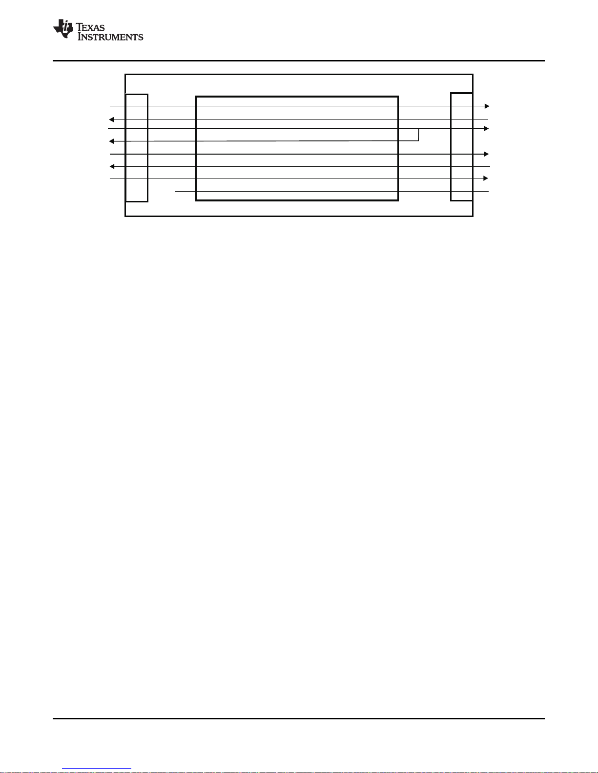
Page 12
TLK3134
4
4
TDP/N[3:0]
RDP/N[3:0]
TD(31..0)
TCLK(3:0)
TC(7..0)
RCLK(3:0)
RD(31..0)
RC(7..0)
(R)GMII/XGMII
XAUI/SerialI/F
TLK3134
SLLS838F–MAY 2007–REVISED DECEMBER 2009
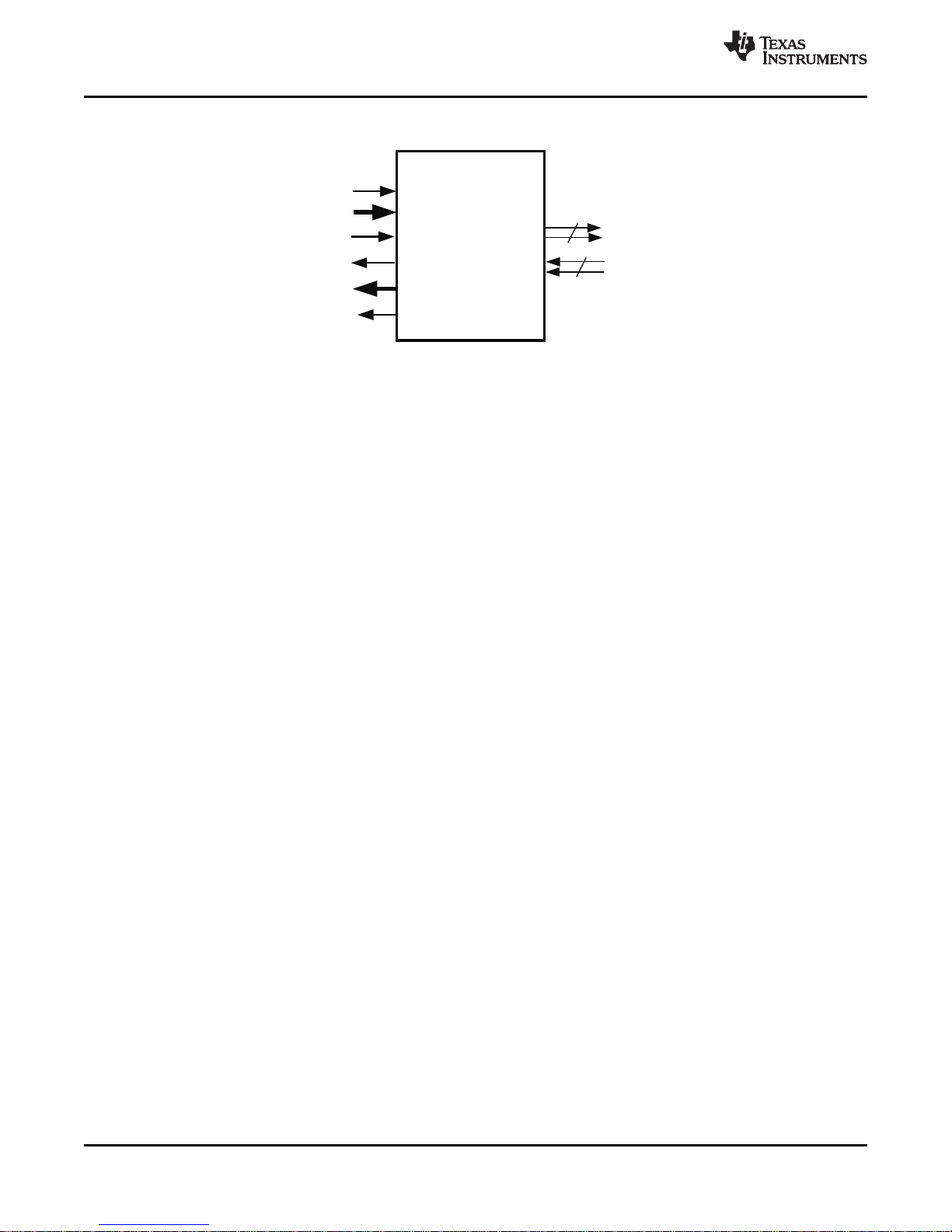
1.3 Pin Out
1.4 Description
The TLK3134 is a flexible four-channel independently configurable serial transceiver. It can be configured
to be compliant with the 10Gbps Ethernet XAUI specification. It can also be configured to be compliant
with the 1000Base-X 1Gbps Ethernet Specification (Auto-Negotiation not supported). The TLK3134
provides high-speed bidirectional point-to-point data transmissions with up to 30 Gbps of raw data
transmission capacity. The primary application of this device is in backplanes and front panel connections
requiring 10Gbps connections over controlled impedance media of approximately 50Ω. The transmission
media can be printed circuit board (PCB) traces, copper cables or fiber-optical media. The ultimate rate
and distance of data transfer is dependent upon the attenuation characteristics of the media and the noise
coupling into the lines.
www.ti.com
The TLK3134 performs the parallel-to-serial, serial-to-parallel conversion, and clock extraction functions
for a physical layer interface. The TLK3134 provides a complete XGXS/PCS function defined in Clause
47/48 of the IEEE 802.3ae 10Gbps Ethernet standard. The TLK3134 also provides 1000Base-X (PCS)
layer functionality described in Clause 36 of 802.3-2002. The serial transmitter is implemented using
differential Current Mode Logic (CML) with integrated termination resistors.
The TLK3134 can be optionally configured as a XAUI or 10GFC transceiver. TLK3134 supports a 32-bit
data path, 4-bit control, 10 Gigabit Media Independent Interface (XGMII) to the protocol device. Figure 1-1
shows an example system block diagram for TLK3134 used to provide the 10Gbps Ethernet Physical
Coding Sublayer to Coarse Wave-length Division Multiplexed optical transceiver or parallel optics.
Many common applications may be enabled by way of externally available control pins. Detailed control of
the TLK3134 on a per channel basis is available by way of accessing a register space of control bits
available through a two-wire access port called the Management Data Input/Output (MDIO) interface.
The PCS (Physical Coding Sublayer) functions such as the CTC FIFO are designed to be compliant for an
IEEE 802.3 XAUI or 1000Base-X PCS link. However, each of the PCS functions may be disabled or
bypassed until the TLK3134 is operating at its most basic state, that of a simple four channel 10-bit
SERDES suitable for a wide range of applications such as CPRI or OBSAI wireless infrastructure links.
The differential output swing for the TLK3134 is suitable for compliance with IEEE 802.3 XAUI links, which
is also suitable for CPRI LV serial links. The TLK3134 provides for setting larger output signal swing
suitable for CPRI HV links by setting an appropriate register bit available though MDIO.
12 Introduction Copyright © 2007–2009, Texas Instruments Incorporated
Submit Documentation Feedback
Product Folder Link(s): TLK3134
Page 13
TLK3134TLK3134
TD(31:0)
TCLK
RCLK
RD(31:0)
LineCard
4
4
4
4
TC(3:0)
RC(3:0)
XAUIBackplane
XAUI
XGMIRX
A
XGMITX
A
MAC/
Packet
Processor
XAUI
CWDMor
Parallel
Optics
LineCard
4
4
4
4
TLK3134
TD(31:0)
RD(31:0)
TCLK
RCLK
RDP/N[3:0]
TDP/N[3:0]
TC(3:0)
TLK3134
TD(31:0)
RD(31:0)
TCLK
RCLK
RDP/N[3:0]
TDP/N[3:0]
TC(3:0)
RC(3:0)
RC(3:0)
MAC/
PACKET
PROCESSOR
FRAMER/
PCS
PHY/
OPTICS
SystemBackplane
SWITCH
FABRIC
TLK3134
www.ti.com
Figure 1-2 shows an example system block diagram for TLK3134 used to provide the system backplane
interconnect.
SLLS838F–MAY 2007–REVISED DECEMBER 2009
Figure 1-1. System Block Diagram – XAUI
Copyright © 2007–2009, Texas Instruments Incorporated Introduction 13
Figure 1-2. System Block Diagram – XAUI Backplane
Submit Documentation Feedback
Product Folder Link(s): TLK3134
Page 14
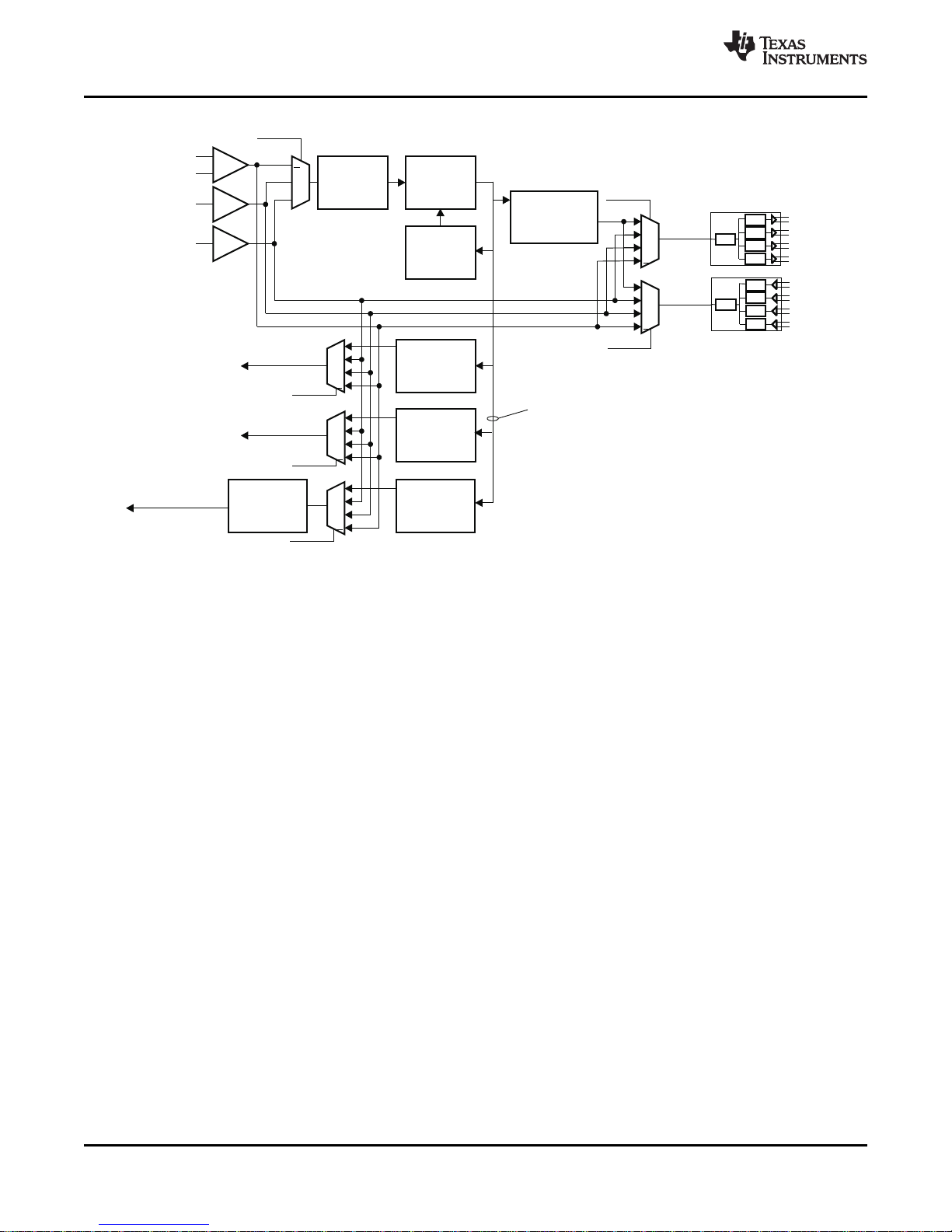
REFCLK_P
REFCLK_N
REFCLK
RXBCLK[0]
REF_SEL[1:0]
REFCLK
Divider
REF_DIV[6:0]
PLL
Feedback
Divider
FB_DIV[6:0]
FirstPLL Output
Divider
RXTX_DIV[6:0]
JitterCleaner
PLL Core
SecondPLL
Output
Divider
RXB_DIV[6:0]
TX_SEL[1:0]
RX_SEL[1:0]
REFCLK_TX
REFCLK_RX
ThirdPLL
Output
Divider
DEL_DIV[6:0]
DELAY_CLK
DEL_SEL[1:0]
RXB_SEL[1:0]
RXBYTE_CLK
00
01
1X
00
01
10
11
00
01
10
11
00
01
10
11
00
01
10
11
(2.875GhzMin.,3GhzTyp.,3.125GhzMax.)
FourthPLL
Output
Divider
HSTL_DIV1[6:0]
HSTL_2X_CLK
HSTL_SEL[1:0]
00
01
10
11
SERDESTX
SERDESRX
TX3P/N
TX2P/N
TX1P/N
TX0P/N
RX3P/N
RX2P/N
RX1P/N
RX0P/N
PLL
P2S
P2S
P2S
P2S
PLL
S2P
S2P
S2P
S2P
Note:DefaultMuxSelects AreUnderlined.
HSTL Output
Divider
HSTL_DIV2[6:0]
TLK3134
SLLS838F–MAY 2007–REVISED DECEMBER 2009
www.ti.com
Figure 1-3. Block Diagram – TLK3134 Clocking Architecture
2 Detailed Description
2.1 Clocking Modes
The TLK3134 contains an internal low-bandwidth, low-jitter high quality LC oscillator that may be
configured as a jitter cleaner. The jitter cleaner oscillator has a high frequency narrow band of operation
that may be used to generate all common reference clock frequencies by way of programmable pre-scaler
and post-scaler registers. In this manner a poor quality input reference clock can be input to the jitter
cleaner which will lock to the reference clock and provide a clean reference to the internal SERDES PLLs.
Appendix A defines in detail the clocking possibilities, and device settings.
Alternatively, the jitter cleaner may be used to lock to a recovered byte clock from RX channel 0 and
remove jitter that may have transferred through the clock/data recovery circuit from the serial data stream
to the recovered byte clock (including parallel output data timing). In this way the recovered byte clock
may be extracted from the serial data stream yet be suitable for use in applications that require a clean
clock source derived from the serial data stream. The TLK3134 jitter cleaner may only be used on the
recovered byte clock from Channel 0. If the jitter cleaner is used to clean the recovered byte clock, it may
not be used to clean the input reference clock, and the PLL at the center of the deserializer core must
have a clean low-jitter reference clock from an external clock source, preferably a low-jitter crystal based
oscillator. Note that the Transmit SERDES macro can run from the cleaned recovered RX channel 0 byte
clock which allows for the outgoing TX serial data rate for all channels to exactly match the incoming data
rate of RX Channel 0.
The TLK3134 clocking architecture allows for bypass of the Jitter cleaner PLL in cases where power or
application board area is critical.
See Figure 1-3 Clocking Architecture for a representation of the use of the jitter cleaner in the TLK3134.
14 Detailed Description Copyright © 2007–2009, Texas Instruments Incorporated
Submit Documentation Feedback
Product Folder Link(s): TLK3134
Page 15

TLK3134
www.ti.com
2.2 Operating Frequency Range
The TLK3134 is optimized for operation at a serial data rate of 600 Mbit/s through 3.75 Gbit/s. The
external differential (optionally single-ended) reference clock has a large operating frequency range
allowing support for many different applications. The reference clock frequency must be within ±200 PPM
of the incoming serial data rate, and have less than 40ps of jitter. Table 2-1 shows a summary of
frequency ranges supported. For more details, see Appendix A. In all applications except XAUI/10GFC,
the transmit parallel clock must be frequency locked (0 ppm) to the supplied REFCLK frequency
(XAUI/10GFC allows ±200 ppm).
Table 2-1. Supported Protocol Rates and REFCLK Values
PROTOCOL Refclk (MHz) LINE RATE (Gbps)
XAUI – 10G Ethernet 78.125/156.25/312.5 3.125
10 Gigabit Fibre Channel 79.6875/159.375/ 318.75 3.1875
1G Ethernet 62.5/125/250 1.25
1X/2X Fibre Channel 53.125/106.25/212.5
OBSAI 76.8/153.6/307.2 1.536
CPRI 61.44/122.88/245.76 1.2288
Generic TBI 50 → 375 MHz 0.600 → 3.75
Generic RTBI 50 → 375 MHz 0.600 → 1.6
Generic NBID/TBID 50 → 375 MHz 0.600 → 3.2
SLLS838F–MAY 2007–REVISED DECEMBER 2009
2.125
1.0625
3.072
0.768
2.4576
0.6144
2.3 CPRI Latency Support
The TLK3134 has a round trip latency measurement capability to support its use in CPRI applications.
When enabled, the TLK3134 will measure the elapsed time from the transmission of a K28.5 code in a
CPRI frame until the reception of a K28.5 code in the receive path. This measurement result may be read
through an MDIO readable register. The measurement has an accuracy of ±4 ns with the Jitter Cleaner
PLL enabled, and an accuracy of ±2 parallel byte clock periods if the Jitter Cleaner PLL is disabled.
2.4 Powerdown Mode
The TLK3134 (through the ENABLE pin and through register control) is capable of going into a low power
quiescent state. In this state, all analog and digital circuitry is disabled.
2.5 Application Examples
TLK3134 supports many different application modes. Detailed register settings per application mode are
shown in Table 2-2. The following application diagrams do not show all possible applications, and are
intended only to illustrate the flexibility of the device.
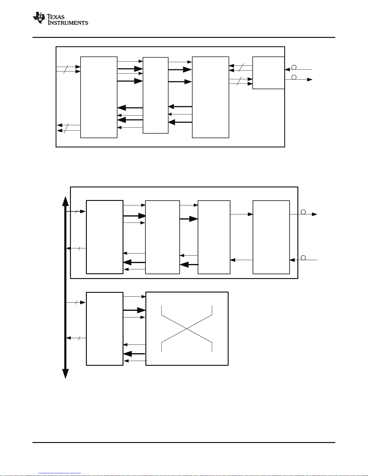
Figure 2-1 shows the TLK3134 in a Quad independent channel SERDES Application. The 1000Base-X
PCS layer can be enabled or disabled. Note that in independent channel mode, the 8B/10B
encoder/decoder functions can either be turned on or turned off. When turned off, either 5 or 10 bits
(DDR/SDR) of data is accepted from and presented to the parallel side. When the 8B/10B
encoder/decoder functions are enabled, 1 bit of control and 8 bits of data are accepted from and
presented to the parallel side using the standardized (R)GMII control characters.
Copyright © 2007–2009, Texas Instruments Incorporated Detailed Description 15
Submit Documentation Feedback
Product Folder Link(s): TLK3134
Page 16
XGMII
10
1
10
1
10
1
10
1
10
1
10
1
10
1
10
1
XAUI
TLK3134
TLK3134
XGXSCORE
36
4
4
XGMII
XAUI
TLK3134
XGXSCORE A
36
4
XGMII
XAUI
TLK3134
SLLS838F–MAY 2007–REVISED DECEMBER 2009
Figure 2-1. Quad 10-Bit SERDES Application
Figure 2-2 shows the TLK3134 in a XAUI Loopback Application. It is possible to configure XAUI side
loopback in SERDES mode for all 4 channels on an individual basis.
www.ti.com
Figure 2-2. XAUI Mode – XAUI (Serial) Loopback Application
Figure 2-3 shows the TLK3134 in a XGMII Loopback Application. It is possible to configure XGMII side
loopback in SERDES mode for all 4 channels on an individual basis.
Figure 2-3. XAUI Mode - XGMII (Parallel ) Loopback Application
Figure 2-4 shows the TLK3134 in a custom application example with mixed modes per Channel.
• Channel 1 in Parallel independent loopback mode
• Channel 3 in Serial independent loopback mode
• Channel 0 & 2 in independent channel transceiver mode
16 Detailed Description Copyright © 2007–2009, Texas Instruments Incorporated
Submit Documentation Feedback
Product Folder Link(s): TLK3134
Page 17
PARALLEL
XGXSCORE
LANE0
LANE1
LANE2
LANE3
SERIAL
TLK3134
TLK3134
www.ti.com
The TLK3134 supports the IEEE 802.3 defined Management Data Input/Output (MDIO) Interface to allow
ease in configuration and status monitoring of the link. The bi-directional data pin (MDIO) must be
externally pulled up to 1.2 V or 2.5 V (VDDM) per the standard for MDIO.
The TLK3134 supports the IEEE 1149.1/1149.6 defined JTAG test port for ease in board manufacturing
test. It also supports a comprehensive series of built-in tests for self-test purposes including PRBS
generation and verification, CRPAT, CJPAT, Mixed/High/Low Frequency testing.
SLLS838F–MAY 2007–REVISED DECEMBER 2009
Figure 2-4. Custom Independent Configuration Application
The TLK3134 operates with a 1.2 V core voltage supply, a 1.5/1.8 V HSTL I/O voltage supply and a 2.5 V
LVCMOS/bias supply.
The TLK3134 is packaged in a 19×19mm, 289-ball, 1mm ball pitch Plastic Ball Grid Array (PBGA)
package and is characterized for operation from –40°C to 85°C Ambient, 105°C Junction, and 5% power
supply variation at the balls of the device unless noted otherwise.
The following block diagram provides a high level description of the TLK3134.
Copyright © 2007–2009, Texas Instruments Incorporated Detailed Description 17
Submit Documentation Feedback
Product Folder Link(s): TLK3134
Page 18
XGMII/
GMII/
RGMII/
TBI/
RTBI
TX
TXD(31:0)
XGMII/
GMII/
RGMII/
TBI/
RTBI
RX
RXD(31:0)
Serial
I/F
Core
MDIO
PRTAD[4:0]
MDIO
MDC
JTAG
TCK
TDI
TMS
TRSTN
TDO
TDP[3:0]
TDN[3:0]
4
TCLK(3:0)
RCLK(3:0)
4
TXC(7:0)
RXC(7:0)
XAUICore+
1000Base-XPCS
RDN[3:0]
RDP[3:0]
Jitter
Cleaner
PLL
TDP3/TDN3
RDP3/RDN3
CHANNEL 3
Test
mode
TDP2/TDN2
RDP2/RDN2
CHANNEL 2
Test
mode
TDP1/TDN1
RDP1/RDN1
CHANNEL 1
Test
mode
Self
Test
SERDES
Core
TCLK
TXD[7:0]
8Bit
10Bit
RCLK
REFCLKP
REFCLKN
8b/10b
Decoding
And
SelfTest
Verification/
Reporting
RX
FIFO
/
CTC
RCLK
RXD(7:0)
TDP0
TDN0
RDP0
RDN0
RCLK
CHANNEL 0
10Bit
Test
mode
8Bit
8b/
10b
enc
TX
FIFO
/
CTC
TLK3134
SLLS838F–MAY 2007–REVISED DECEMBER 2009
www.ti.com
Following is a more detailed block diagram description of the XAUI core.
18 Detailed Description Copyright © 2007–2009, Texas Instruments Incorporated
Figure 2-6. Detailed XAUI/1000Base-X Core Block Diagram
Figure 2-5. TLK3134 Block Diagram
Submit Documentation Feedback
Product Folder Link(s): TLK3134
Page 19
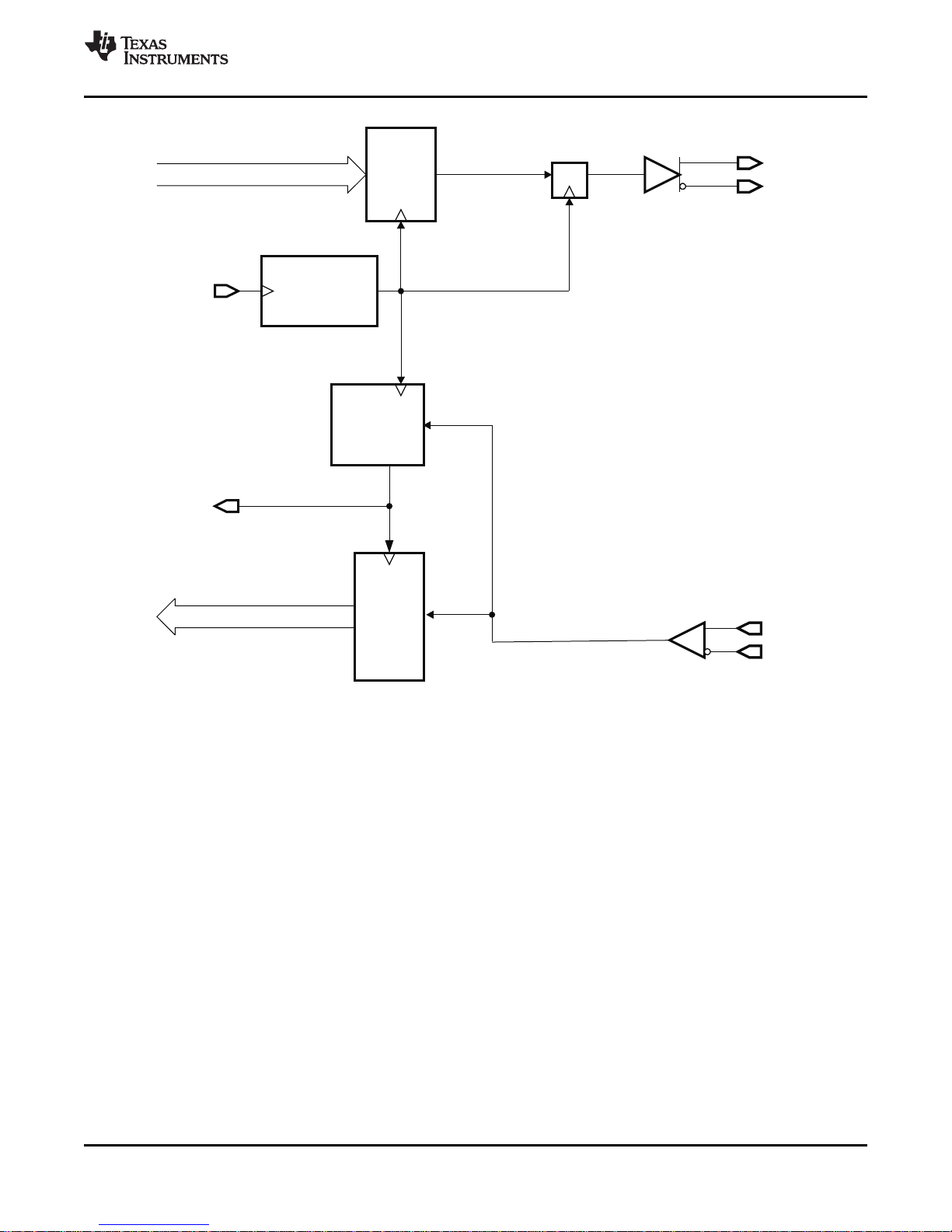
Parallel
toSerial
REFCLKP
/
N
Baud
Clock
D Q
Serialto
Parallel
and
Comma
Detect
Interpolator
andClock
Recovery
Multiplying
Clock
Synthesizer
RCLK
Recovered
Clock
TDP
TDN
RDP
RDN
ParallelDataIn
ParallelDataOut
TLK3134
www.ti.com
SLLS838F–MAY 2007–REVISED DECEMBER 2009
Copyright © 2007–2009, Texas Instruments Incorporated Detailed Description 19
Figure 2-7. Block Diagram of SERDES Core
Submit Documentation Feedback
Product Folder Link(s): TLK3134
Page 20
TLK3134
SLLS838F–MAY 2007–REVISED DECEMBER 2009
www.ti.com
2.6 Device Operation Modes
Table 2-2. Device Operation Modes
(1)
DEVICE MODE (DDR (SDR (SDR
ST Primary Chip Input 0 1
MDIO Access Method Clause 45 Clause 22
XAUI_ORDER 32809.15
Logical Or w/CODE pin
XAUI_TX_EDGE_ALIGN 32808.15
XAUI_RX_EDGE_ALIGN 32808.11
DDR_SDR 17.5 1 0 1 0 1 0 1 0 X
NIBBLE_ORDER 17.4 0/1 X 0/1 X 0/1 X 0/1 X
TX_EDGE_MODE 17.1
RX_EDGE_MODE 17.0
FC_ENC_MODE 17.6 0 0/1 0 0/1
COMMA_DET_EN 17.7 0/1 0 1 0/1 1
PCS_EN 17.3 Logical OR w/CODE pin 1 0
ENC_DEC_EN 17.2 0 1 0 1
BUSWIDTH 36864.7 0 1 0
FULL_DDR 17.9 0 1
Legend : (X = Don’t Care) — (0 = Must Be Zero) — (1 = Must Be One) — (0/1 = Can Be Either Zero-or-One)
XAUI
(DDR) (DDR) (DDR) (SDR) (DDR) (SDR) (DDR) (DDR) (DDR)
1 0
0/1
X
10GFC
(2)
RGMII GMII REBI EBI RNBI TBID NBID
(1) Default Mode if ST Primary Chip Input Pin “0”, CODE Primary Chip Input Pin “1”.
(2) Default Mode if ST Primary Chip Input Pin “0”, CODE Primary Chip Input Pin “0”.
(3) All Clause 22 Registers are Per Device Channel.
RTBI TBI NBI
) ) )
(3)
X
0/1
20 Detailed Description Copyright © 2007–2009, Texas Instruments Incorporated
Submit Documentation Feedback
Product Folder Link(s): TLK3134
Page 21
TLK3134
www.ti.com
SLLS838F–MAY 2007–REVISED DECEMBER 2009
2.7 Parallel Interface Modes - Detailed Description
The TLK3134 has several parallel interface modes. The major parallel interface modes of operation are
presented below:
2.7.1 XAUI/10GFC Mode
Table 2-3. XAUI – Lane To Functional Pin Mapping (XAUI_ORDER = 1)
XAUI LANE CONTROL BIT DATA BYTE CONTROL BIT CONTROL BYTE CLOCK CLOCK
Lane 3 TXC_[3] TXD_[31:24] RXC_[3] RXD_[31:24] TXCLK_[1] RXCLK_[1]
Lane 2 TXC_[2] TXD_[23:16] RXC_[2] RXD_[23:16] TXCLK_[1] RXCLK_[1]
Lane 1 TXC_[1] TXD_[15:8] RXC_[1] RXD_[15:8] TXCLK_[1] RXCLK_[1]
Lane 0 TXC_[0] TXD_[7:0] RXC_[0] RXD_[7:0] TXCLK_[1] RXCLK_[1]
10GFC LANE CONTROL BIT DATA BYTE CONTROL BIT CONTROL BYTE CLOCK CLOCK
Lane 0 TXC_[3] TXD_[31:24] RXC_[3] RXD_[31:24] TXCLK_[1] RXCLK_[1]
Lane 1 TXC_[2] TXD_[23:16] RXC_[2] RXD_[23:16] TXCLK_[1] RXCLK_[1]
Lane 2 TXC_[1] TXD_[15:8] RXC_[1] RXD_[15:8] TXCLK_[1] RXCLK_[1]
Lane 3 TXC_[0] TXD_[7:0] RXC_[0] RXD_[7:0] TXCLK_[1] RXCLK_[1]
TRANSMIT TRANSMIT RECEIVE RECEIVE TRANSMIT RECEIVE
(INPUT) (INPUT) (OUTPUT) (OUTPUT) (INPUT) (OUTPUT)
Table 2-4. 10GFC – Lane To Functional Pin Mapping (XAUI_ORDER = 0)
TRANSMIT TRANSMIT RECEIVE RECEIVE TRANSMIT RECEIVE
(INPUT) (INPUT) (OUTPUT) (OUTPUT) (INPUT) (OUTPUT)
Copyright © 2007–2009, Texas Instruments Incorporated Detailed Description 21
Submit Documentation Feedback
Product Folder Link(s): TLK3134
Page 22
TXCLK_[0]
{TX_EN,Data0[3:0]}
{TX_EN^TX_ER,
Data0[7:4]}
{TX_EN,Data1[3:0]}
{TX_EN^TX_ER,
Data1[7:4]}
TXD_[4:0]
RXCLK_[0]
{RX_DV,Data0[3:0]}
{RX_DV^RX_ER,
Data0[7:4]}
{RX_DV,Data1[3:0]}
{RX_DV^RX_ER,
Data1[7:4]}
RXD_[4:0]
DDRSourceCenteredTiming
NibbleOrder=1(Default)
TXCLK_[0]
{TX_EN,Data0[3:0]}
{TX_EN^TX_ER,
Data0[7:4]}
{TX_EN,Data1[3:0]}
{TX_EN^TX_ER,
Data1[7:4]}
TXD_[4:0]
RXCLK_[0]
{RX_DV,Data0[3:0]}
{RX_DV^RX_ER,
Data0[7:4]}
{RX_DV,Data1[3:0]}
{RX_DV^RX_ER,
Data1[7:4]}
RXD_[4:0]
DDRSource AlignedTiming
NibbleOrder=1(Default)
Note:IfNibbleOrder=0,thepictureis
thesameexceptthat
{TX_EN,DataN[3:0]}and
{TX_EN^TX_ER,DataN[7:4]}swap
locations.
Note:IfNibbleOrder=0,thepictureis
thesameexceptthat
{RX_DV,DataN[3:0]}and
{RX_DV^RX_ER,DataN[7:4]}swap
locations.
Note:IfNibbleOrder=0,thepictureis
thesameexceptthat
{TX_EN,DataN[3:0]}and
{TX_EN^TX_ER,DataN[7:4]}swap
locations.
Note:IfNibbleOrder=0,thepictureis
thesameexceptthat
{RX_DV,DataN[3:0]}and
{RX_DV^RX_ER,DataN[7:4]}swap
locations.
TLK3134
SLLS838F–MAY 2007–REVISED DECEMBER 2009
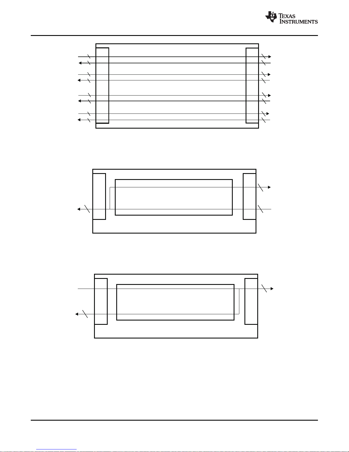
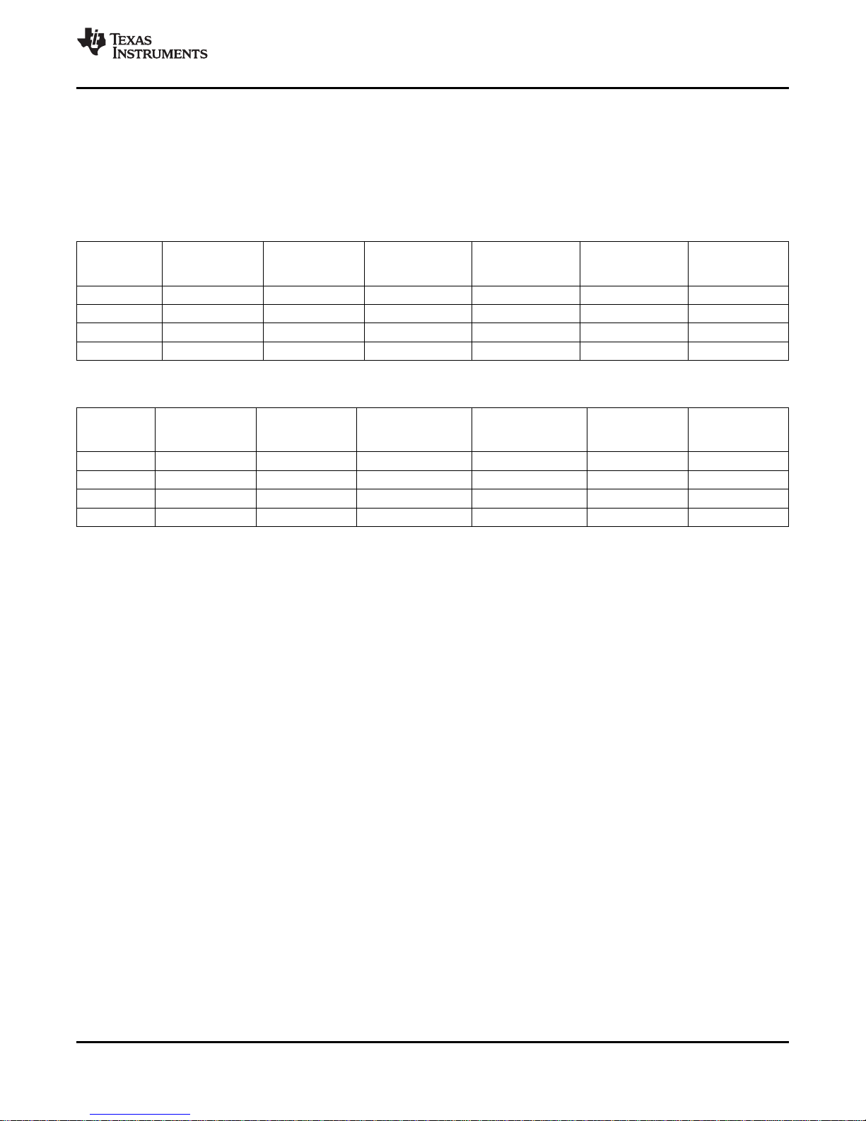
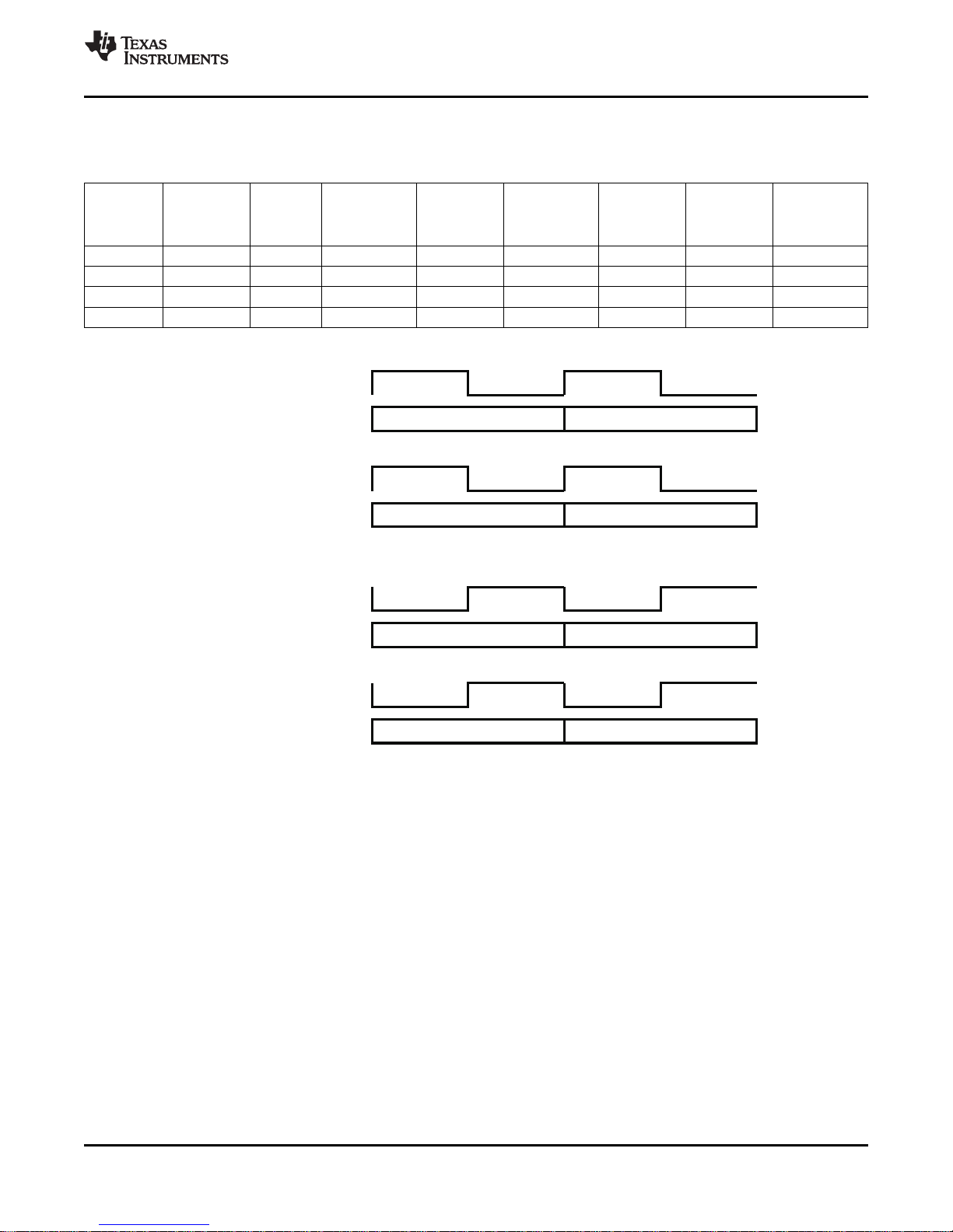
2.7.2 RGMII Mode (Reduced Gigabit Media Independent Interface)
Table 2-5. RGMII – Lane To Functional Pin Mapping
DATA TX_EN/TX_ER TRANSMIT RX_DV/RX_ER TRANSMIT RECEIVE
CHANNEL CONTROL BIT DATA NIBBLE CONTROL BIT CLOCK CLOCK
NUMBER (INPUT) (INPUT) (OUTPUT) (INPUT) (OUTPUT)
Channel 0 TXD_[4] TXD_[3:0] RXD_[4] RXD_[3:0] TXCLK_[0] RXCLK_[0]
Channel 1 TXD_[12] TXD_[11:8] RXD_[12] RXD_[11:8] TXCLK_[1] RXCLK_[1]
Channel 2 TXD_[20] TXD_[19:16] RXD_[20] RXD_[19:16] TXCLK_[2] RXCLK_[2]
Channel 3 TXD_[28] TXD_[27:24] RXD_[28] RXD_[27:24] TXCLK_[3] RXCLK_[3]
RECEIVE
CONTROL
NIBBLE
(OUTPUT)
www.ti.com
Figure 2-8. RGMII – Individual Channel Byte Ordering – Channel 0 Example
22 Detailed Description Copyright © 2007–2009, Texas Instruments Incorporated
Submit Documentation Feedback
Product Folder Link(s): TLK3134
Page 23
TXCLK_[0]
Data0[4:0] Data0[9:5]
TXD_[4:0]
RXCLK_[0]
Data0[4:0] Data0[9:5]
RXD_[4:0]
DDRSourceCenteredTiming
(NibbleOrder=1Default)
TXCLK_[0]
TXD_[4:0]
RXCLK_[0]
RXD_[4:0]
DDRSource AlignedTiming
(NibbleOrder=1Default)
Data0[4:0] Data0[9:5]
Data0[4:0] Data0[9:5]
TXCLK_[0]
Data0[4:0]Data0[9:5]
TXD_[4:0]
RXCLK_[0]
Data0[4:0]Data0[9:5]
RXD_[4:0]
DDRSourceCenteredTiming
(NibbleOrder=0)
TXCLK_[0]
TXD_[4:0]
RXCLK_[0]
RXD_[4:0]
DDRSource AlignedTiming
(NibbleOrder=0)
Data0[4:0]Data0[9:5]
Data0[4:0]Data0[9:5]
TLK3134
www.ti.com
SLLS838F–MAY 2007–REVISED DECEMBER 2009
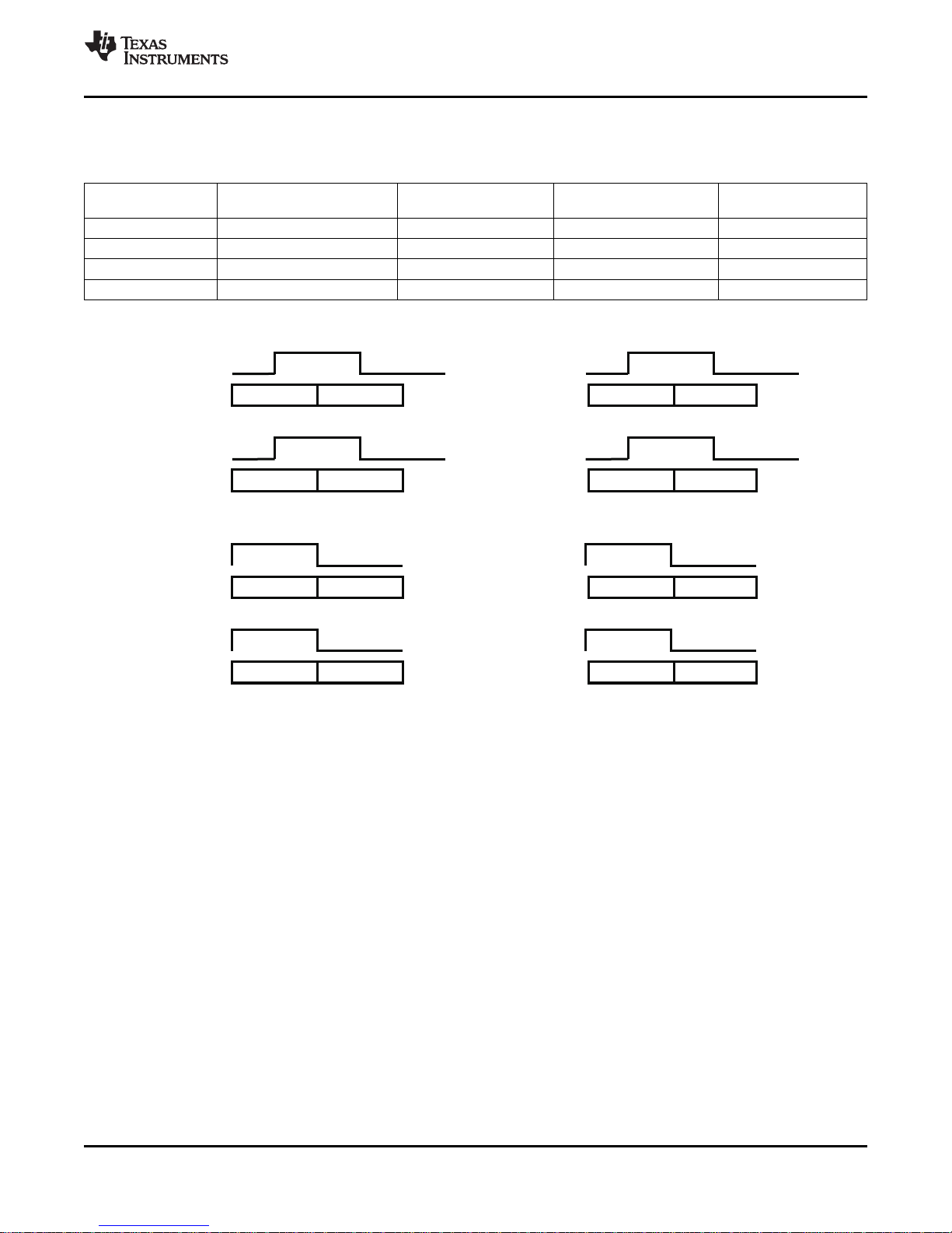
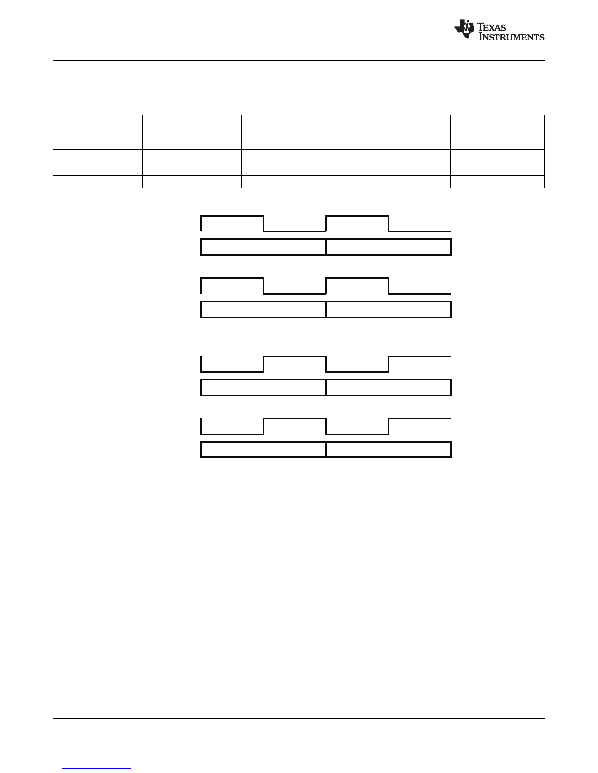
2.7.3 RTBI Mode (Reduced Ten Bit Interface)
Table 2-6. RTBI – Lane To Functional Pin Mapping
DATA CHANNEL TRANSMIT DATA 5 BITS RECEIVE DATA 5 BITS TRANSMIT CLOCK RECEIVE CLOCK
NUMBER (INPUT) (OUTPUT) (INPUT) (OUTPUT)
Channel 0 TXD_[4:0] RXD_[4:0] TXCLK_[0] RXCLK_[0]
Channel 1 TXD_[12:8] RXD_[12:8] TXCLK_[1] RXCLK_[1]
Channel 2 TXD_[20:16] RXD_[20:16] TXCLK_[2] RXCLK_[2]
Channel 3 TXD_[28:24] RXD_[28:24] TXCLK_[3] RXCLK_[3]
Figure 2-9. RTBI – Individual Channel Byte Ordering – Channel 0 Example
Copyright © 2007–2009, Texas Instruments Incorporated Detailed Description 23
Submit Documentation Feedback
Product Folder Link(s): TLK3134
Page 24
TXCLK_[0]
TXC_[4],TXC_[0],TXD_[7:0]
RXCLK_[0]
RXC_[4],RXC_[0],RXD_[7:0]
SDRRisingEdge AlignedTiming
TXCLK_[0]
TXC_[4],TXC_[0],TXD_[7:0]
RXCLK_[0]
RXC_[4],RXC_[0],RXD_[7:0]
SDRFallingEdge AlignedTiming
Data0[9:0] Data1[9:0]
Data0[9:0] Data1[9:0]
Data0[9:0] Data1[9:0]
Data0[9:0] Data1[9:0]
TLK3134
SLLS838F–MAY 2007–REVISED DECEMBER 2009
www.ti.com
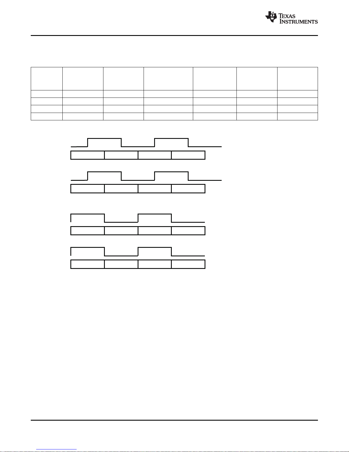
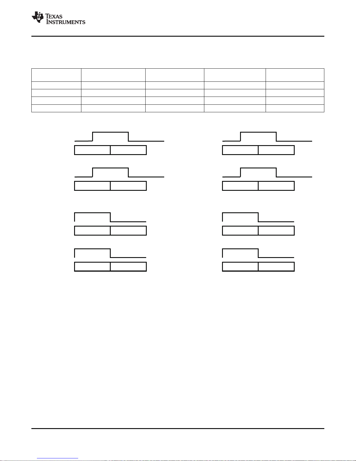
2.7.4 TBI Mode (Ten Bit Interface)
Table 2-7. TBI – Lane To Functional Pin Mapping
DATA CHANNEL TRANSMIT DATA 10 BITS RECEIVE DATA 10 BITS TRANSMIT CLOCK RECEIVE CLOCK
NUMBER (INPUT) (OUTPUT) (INPUT) (OUTPUT)
Channel 0 {TXC_[4], TXC_[0],TXD_[7:0]} {RXC_[4], RXC_[0],RXD_[7:0]} TXCLK_[0] RXCLK_ [0]
Channel 1 {TXC_[5],TXC_[1],TXD_[15:8]} {RXC_[5], RXC_[1],RXD_[15:8]} TXCLK_[1] RXCLK_ [1]
Channel 2 {TXC_[6],TXC_[2],TXD_[23:16]} {RXC_[6],RXC_[2],RXD_[23:16]} TXCLK_[2] RXCLK_ [2]
Channel 3 {TXC_[7],TXC_[3],TXD_[31:24]} {RXC_[7],RXC_[3],RXD_[31:24]} TXCLK_[3] RXCLK_ [3]
Figure 2-10. TBI – Individual Channel Byte Ordering – Channel 0 Example
24 Detailed Description Copyright © 2007–2009, Texas Instruments Incorporated
Submit Documentation Feedback
Product Folder Link(s): TLK3134
Page 25
TXCLK_[0]
TXC_[0],TXC_[4],TXD_[7:0]
RXCLK_[0]
RXC_[0],RXC_[4],RXD_[7:0]
TXCLK_[0]
TXC_[0],TXC_[4],TXD_[7:0]
RXCLK_[0]
RXC_[0],RXC_[4],RXD_[7:0]
SDRRisingEdge AlignedTiming
SDRFallingEdge AlignedTiming
{TX_EN,TX_ER,Data0[7:0]} {TX_EN,TX_ER,Data1[7:0]}
{RX_DV,RX_ER,Data0[7:0]} {RX_DV,RX_ER,Data1[7:0]}
{TX_EN,TX_ER,Data0[7:0]} {TX_EN,TX_ER,Data1[7:0]}
{RX_DV,RX_ER,Data0[7:0]} {RX_DV,RX_ER,Data1[7:0]}
TLK3134
www.ti.com
SLLS838F–MAY 2007–REVISED DECEMBER 2009
2.7.5 GMII Mode (Gigabit Media Independent Interface)
Table 2-8. GMII – Lane To Functional Pin Mapping
DATA TRANSMIT RX_ER RECEIVE TRANSMIT RECEIVE
CHANNEL DATA BYTE CONTROL BIT DATA BYTE CLOCK CLOCK
NUMBER (INPUT) (OUTPUT) (OUTPUT) (INPUT) (OUTPUT)
Channel 0 TXC_[0] TXC_[4] TXD_[7:0] RXC_[0] RXC_[4] RXD_[7:0] TXCLK_[0] RXCLK_[0]
Channel 1 TXC_[1] TXC_[5] TXD_[15:8] RXC_[1] RXC_[5] RXD_[15:8] TXCLK_[1] RXCLK_[1]
Channel 2 TXC_[2] TXC_[6] TXD_[23:16] RXC_[2] RXC_[6] RXD_[23:16] TXCLK_[2] RXCLK_[2]
Channel 3 TXC_[3] TXC_[7] TXD_[31:24] RXC_[3] RXC_[7] RXD_[31:24] TXCLK_[3] RXCLK_[3]
TX_EN TX_ER RX_DV
CONTROL CONTROL CONTROL
BIT BIT BIT
(INPUT) (INPUT) (OUTPUT)
Figure 2-11. GMII – Individual Channel Byte Ordering – Channel 0 Example
Copyright © 2007–2009, Texas Instruments Incorporated Detailed Description 25
Submit Documentation Feedback
Product Folder Link(s): TLK3134
Page 26
TXCLK_[0]
Data0[7:0]
TXD_[7:0]
RXCLK_[0]
RXD_[7:0]
SDRRisingEdge AlignedTiming
TXCLK_[0]
TXD_[7:0]
RXCLK_[0]
RXD_[7:0]
SDRFallingEdge AlignedTiming
Data1[7:0]
Data0[7:0] Data1[7:0]
Data0[7:0] Data1[7:0]
Data0[7:0] Data1[7:0]
TLK3134
SLLS838F–MAY 2007–REVISED DECEMBER 2009
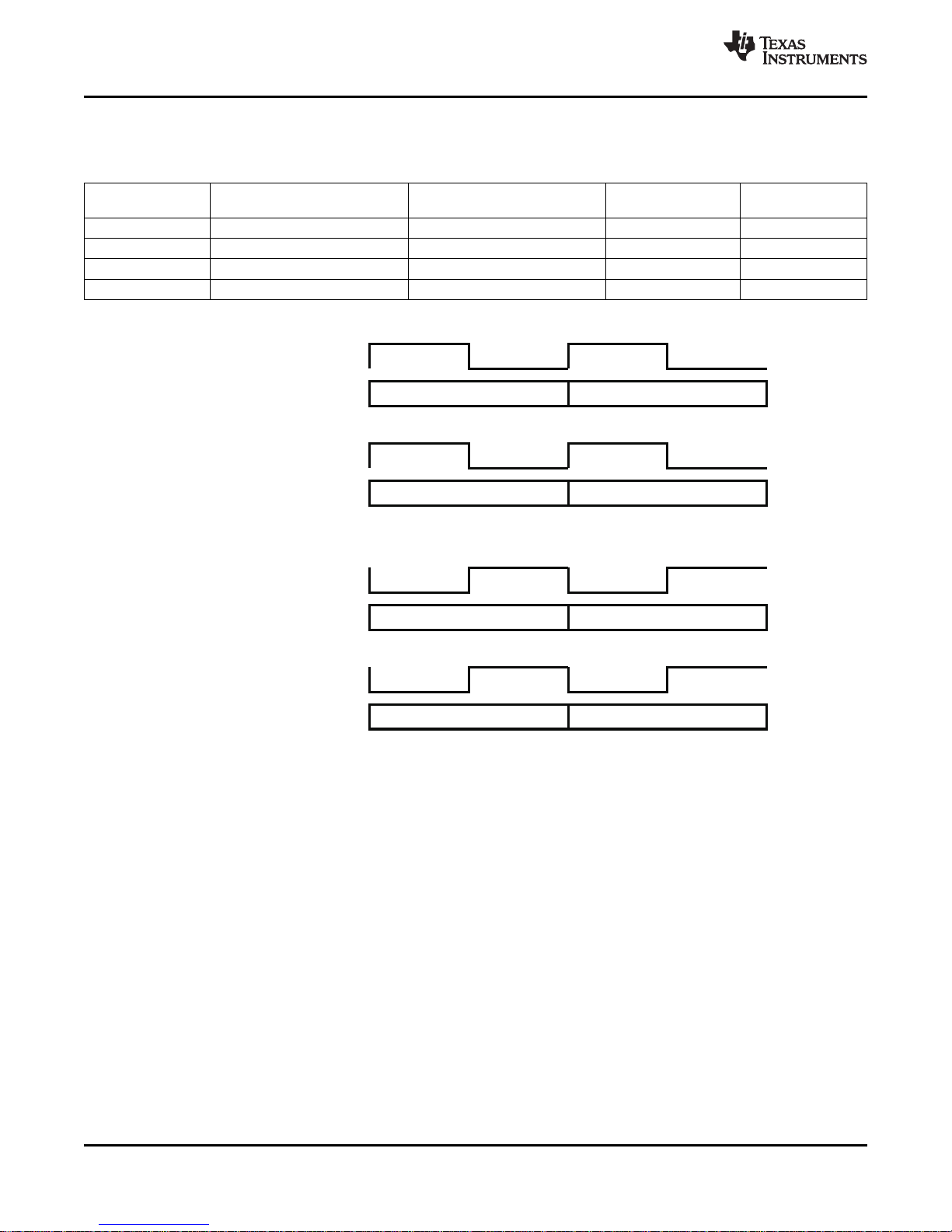
2.7.6 EBI Mode (Eight Bit Interface)
Table 2-9. EBI – Lane To Functional Pin Mapping
DATA CHANNEL TRANSMIT DATA 8 BITS RECEIVE DATA 8 BITS TRANSMIT CLOCK RECEIVE CLOCK
NUMBER (INPUT) (OUTPUT) (INPUT) (OUTPUT)
Channel 0 TXD_[7:0] RXD_[7:0] TXCLK_[0] RXCLK_[0]
Channel 1 TXD_[15:8] RXD_[15:8] TXCLK_[1] RXCLK_[1]
Channel 2 TXD_[23:16] RXD_[23:16] TXCLK_[2] RXCLK_[2]
Channel 3 TXD_[31:24] RXD_[31:24] TXCLK_[3] RXCLK_[3]
www.ti.com
Figure 2-12. EBI – Individual Channel Byte Ordering – Channel 0 Example
26 Detailed Description Copyright © 2007–2009, Texas Instruments Incorporated
Submit Documentation Feedback
Product Folder Link(s): TLK3134
Page 27
TXCLK_[0]
Data0[3:0] Data0[7:4]
TXD_[3:0]
RXCLK_[0]
Data0[3:0] Data0[7:4]
RXD_[3:0]
DDRSourceCenteredTiming
(NibbleOrder=1Default)
TXCLK_[0]
TXD_[3:0]
RXCLK_[0]
RXD_[3:0]
DDRSource AlignedTiming
(NibbleOrder=1Default)
Data0[3:0] Data0[7:4]
Data0[3:0] Data0[7:4]
TXCLK_[0]
TXD_[3:0]
RXCLK_[0]
RXD_[3:0]
DDRSourceCenteredTiming
(NibbleOrder=0)
TXCLK_[0]
TXD_[3:0]
RXCLK_[0]
RXD_[3:0]
DDRSource AlignedTiming
(NibbleOrder=0)
Data0[3:0]Data0[7:4]
Data0[3:0]Data0[7:4]
Data0[3:0]Data0[7:4]
Data0[3:0]Data0[7:4]
TLK3134
www.ti.com
SLLS838F–MAY 2007–REVISED DECEMBER 2009
2.7.7 REBI Mode (Reduced Eight Bit Interface)
Table 2-10. REBI – Lane To Functional Pin Mapping
DATA CHANNEL TRANSMIT DATA 4 BITS RECEIVE DATA 4 BITS TRANSMIT CLOCK RECEIVE CLOCK
NUMBER (INPUT) (OUTPUT) (INPUT) (OUTPUT)
Channel 0 TXD_[3:0] RXD_[3:0] TXCLK_[0] RXCLK_[0]
Channel 1 TXD_[11:8] RXD_[11:8] TXCLK_[1] RXCLK_[1]
Channel 2 TXD_[19:16] RXD_[19:16] TXCLK_[2] RXCLK_[2]
Channel 3 TXD_[27:24] RXD_[27:24] TXCLK_[3] RXCLK_[3]
Figure 2-13. REBI – Individual Channel Byte Ordering – Channel 0 Example
Copyright © 2007–2009, Texas Instruments Incorporated Detailed Description 27
Submit Documentation Feedback
Product Folder Link(s): TLK3134
Page 28
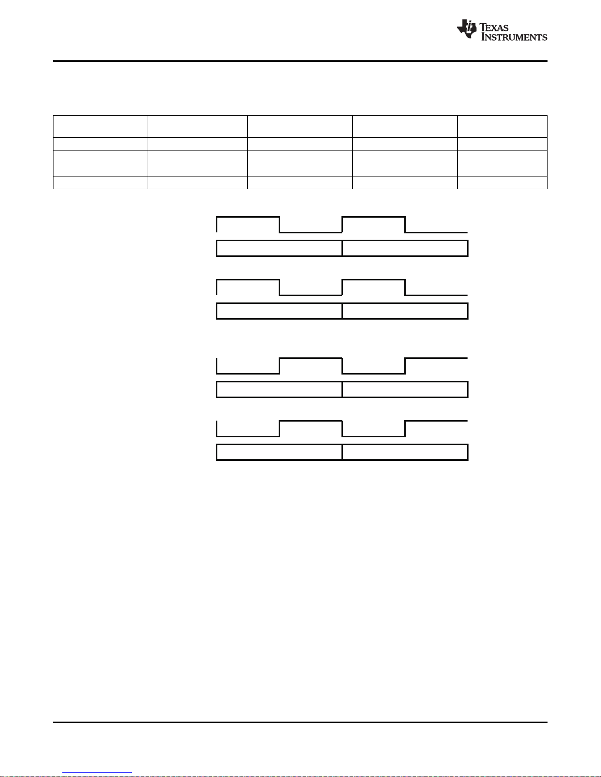
TXCLK_[0]
TXC_[0],TXD_[7:0]
RXCLK_[0]
RXC_[0],RXD_[7:0]
SDRRisingEdge AlignedTiming
TXCLK_[0]
TXC_[0],TXD_[7:0]
RXCLK_[0]
RXC_[0],RXD_[7:0]
SDRFallingEdge AlignedTiming
Data0[8:0]={ControlBit,DataByte} Data1[8:0]={ControlBit,DataByte}
Data0[8:0]={ControlBit,DataByte} Data1[8:0]={ControlBit,DataByte}
Data0[8:0]={ControlBit,DataByte} Data1[8:0]={ControlBit,DataByte}
Data0[8:0]={ControlBit,DataByte} Data1[8:0]={ControlBit,DataByte}
TLK3134
SLLS838F–MAY 2007–REVISED DECEMBER 2009
2.7.8 NBI Mode (Nine Bit Interface Mode)
Table 2-11. NBI – Lane To Functional Pin Mapping
DATA CHANNEL TRANSMIT DATA 9 BITS RECEIVE DATA 9 BITS TRANSMIT CLOCK RECEIVE CLOCK
NUMBER (INPUT) (OUTPUT) (INPUT) (OUTPUT)
Channel 0 {TXC_[0],TXD_[7:0]} {RXC_[0],RXD_[7:0]} TXCLK_[0] RXCLK_[0]
Channel 1 {TXC_[1],TXD_[15:8]} {RXC_[1],RXD_[15:8]} TXCLK_[1] RXCLK_[1]
Channel 2 {TXC_[2],TXD_[23:16]} {RXC_[2],RXD_[23:16]} TXCLK_[2] RXCLK_[2]
Channel 3 {TXC_[3],TXD_[31:24]} {RXC_[3],RXD_[31:24]} TXCLK_[3] RXCLK_[3]
www.ti.com
Figure 2-14. NBI – Individual Channel Byte Ordering – Channel 0 Example
28 Detailed Description Copyright © 2007–2009, Texas Instruments Incorporated
Submit Documentation Feedback
Product Folder Link(s): TLK3134
Page 29
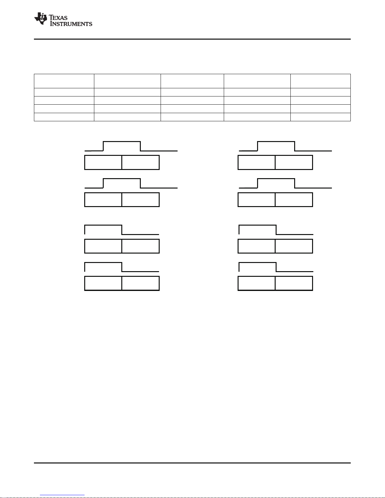
TXCLK_[0]
Data0[4:0]=
{DataByte[4:0]}
Data0[8:5]=
{ControlBit,Data
Byte[7:5]}
TXD_[4:0]
RXCLK_[0]
RXD_[4:0]
DDRSourceCenteredTiming
(NibbleOrder=1Default)
TXCLK_[0]
TXD_[4:0]
RXCLK_[0]
RXD_[4:0]
DDRSource AlignedTiming
(NibbleOrder=1Default)
TXCLK_[0]
TXD_[4:0]
RXCLK_[0]
RXD_[4:0]
DDRSourceCenteredTiming
(NibbleOrder=0)
TXCLK_[0]
TXD_[4:0]
RXCLK_[0]
RXD_[4:0]
DDRSource AlignedTiming
(NibbleOrder=0)
Data0[4:0]=
{DataByte[4:0]}
Data0[8:5]=
{ControlBit,Data
Byte[7:5]}
Data0[4:0]=
{DataByte[4:0]}
Data0[8:5]=
{ControlBit,Data
Byte[7:5]}
Data0[4:0]=
{DataByte[4:0]}
Data0[8:5]=
{ControlBit,Data
Byte[7:5]}
Data0[4:0]=
{DataByte[4:0]}
Data0[4:0]=
{DataByte[4:0]}
Data0[4:0]=
{DataByte[4:0]}
Data0[4:0]=
{DataByte[4:0]}
Data0[8:5]=
{ControlBit,Data
Byte[7:5]}
Data0[8:5]=
{ControlBit,Data
Byte[7:5]}
Data0[8:5]=
{ControlBit,Data
Byte[7:5]}
Data0[8:5]=
{ControlBit,Data
Byte[7:5]}
TLK3134
www.ti.com
SLLS838F–MAY 2007–REVISED DECEMBER 2009
2.7.9 RNBI Mode (Reduced Nine Bit Interface)
Table 2-12. RNBI – Lane To Functional Pin Mapping
DATA CHANNEL TRANSMIT DATA 5 BITS RECEIVE DATA 5 BITS TRANSMIT CLOCK RECEIVE CLOCK
NUMBER (INPUT) (OUTPUT) (INPUT) (OUTPUT)
Channel 0 TXD_[4:0] RXD_[4:0] TXCLK_[0] RXCLK_[0]
Channel 1 TXD_[12:8] RXD_[12:8] TXCLK_[1] RXCLK_[1]
Channel 2 TXD_[20:16] RXD_[20:16] TXCLK_[2] RXCLK_[2]
Channel 3 TXD_[28:24] RXD_[28:24] TXCLK_[3] RXCLK_[3]
Figure 2-15. RNBI – Individual Channel Byte Ordering – Channel 0 Example
Copyright © 2007–2009, Texas Instruments Incorporated Detailed Description 29
Submit Documentation Feedback
Product Folder Link(s): TLK3134
Page 30
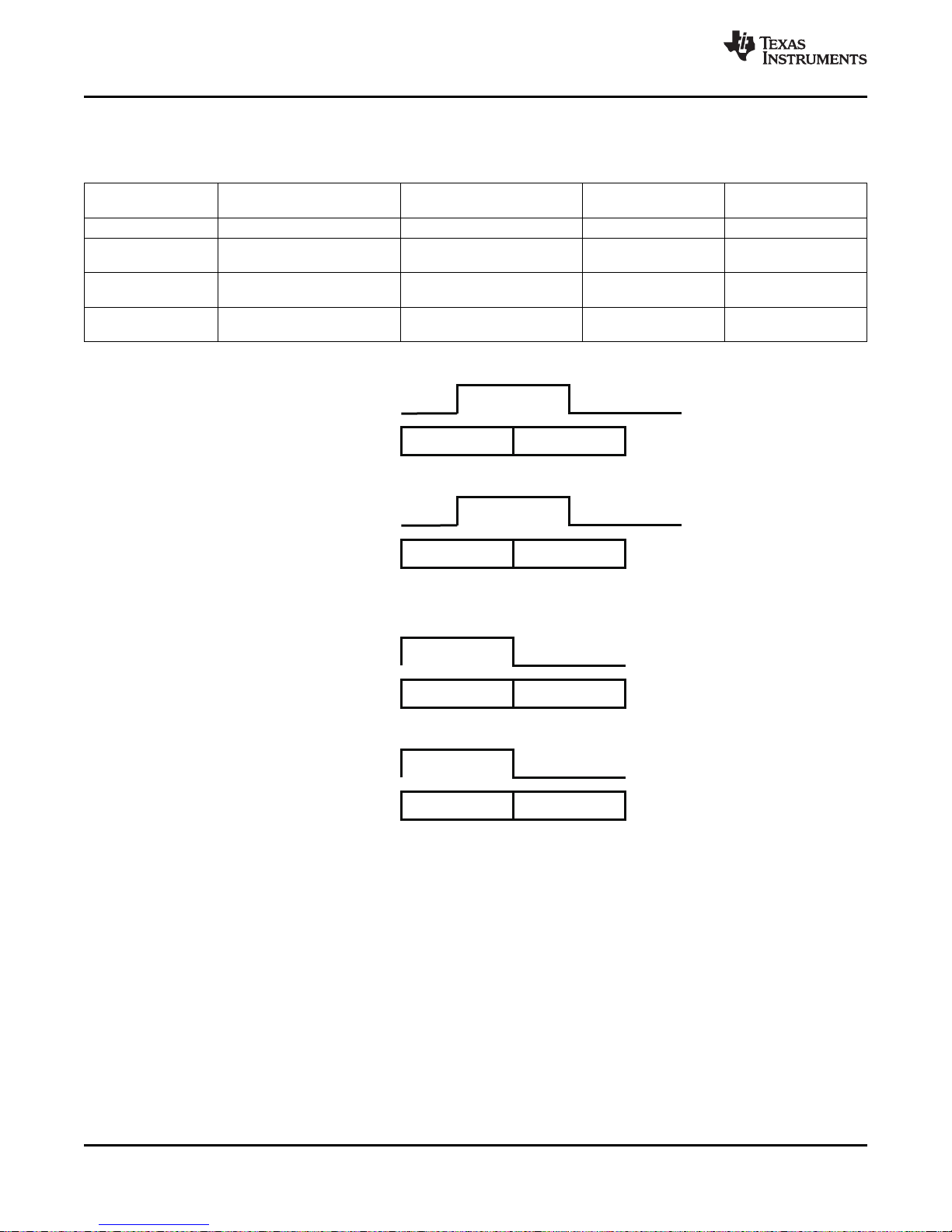
TXCLK_[0]
Data0[9:0] Data1[9:0]
TXC_[4],TXC_[0],
TXD_[7:0]
RXCLK_[0]
Data0[9:0] Data1[9:0]
RXC_[4],RXC_[0],
RXD_[7:0]
DDRSourceCenteredTiming
TXCLK_[0]
TXC_[4],TXC_[0],
TXD_[7:0]
RXCLK_[0]
RXC_[4],RXC_[0],
RXD_[7:0]
DDRSource AlignedTiming
Data0[9:0] Data1[9:0]
Data0[9:0] Data1[9:0]
TLK3134
SLLS838F–MAY 2007–REVISED DECEMBER 2009
2.7.10 TBID Mode (Ten Bit Interface DDR)
Table 2-13. TBID – Lane To Functional Pin Mapping
DATA CHANNEL TRANSMIT DATA 10 BITS RECEIVE DATA 10 BITS TRANSMIT CLOCK RECEIVE CLOCK
NUMBER (INPUT) (OUTPUT) (INPUT) (OUTPUT)
Channel 0 {TXC_[4], TXC_[0],TXD_[7:0]} {RXC_[4], RXC_[0],RXD_[7:0]} TXCLK_[0] RXCLK_ [0]
Channel 1 {TXC_[5],TXC_[1],TXD_[15:8]} TXCLK_[1] RXCLK_ [1]
Channel 2 TXCLK_[2] RXCLK_ [2]
Channel 3 TXCLK_[3] RXCLK_ [3]
{TXC_[6],TXC_[2],TXD_[23:16] {RXC_[6],RXC_[2],RXD_[23:1
} 6]}
{TXC_[7],TXC_[3],TXD_[31:24] {RXC_[7],RXC_[3],RXD_[31:2
} 4]}
{RXC_[5],
RXC_[1],RXD_[15:8]}
www.ti.com
30 Detailed Description Copyright © 2007–2009, Texas Instruments Incorporated
Figure 2-16. TBID – Individual Channel Byte Ordering – Channel 0 Example
Submit Documentation Feedback
Product Folder Link(s): TLK3134
Page 31

TXCLK_[0]
Data0[8:0]={Control
Bit,DataByte}
Data1[8:0]={Control
Bit,DataByte}
TXC_[0],TXD_[7:0]
RXCLK_[0]
Data0[8:0]={Control
Bit,DataByte}
Data1[8:0]={Control
Bit,DataByte}
RXC_[0],RXD_[7:0]
DDRSourceCenteredTiming
TXCLK_[0]
TXC_[0],TXD_[7:0]
RXCLK_[0]
RXC_[0],RXD_[7:0]
DDRSource AlignedTiming
Data0[8:0]={Control
Bit,DataByte}
Data1[8:0]={Control
Bit,DataByte}
Data0[8:0]={Control
Bit,DataByte}
Data1[8:0]={Control
Bit,DataByte}
TLK3134
www.ti.com
SLLS838F–MAY 2007–REVISED DECEMBER 2009
2.7.11 NBID Mode (Nine Bit Interface DDR)
Table 2-14. NBID – Lane To Functional Pin Mapping
DATA CHANNEL TRANSMIT DATA 9 BITS RECEIVE DATA 9 BITS TRANSMIT CLOCK RECEIVE CLOCK
NUMBER (INPUT) (OUTPUT) (INPUT) (OUTPUT)
Channel 0 {TXC_[0],TXD_[7:0]} {RXC_[0],RXD_[7:0]} TXCLK_[0] RXCLK_ [0]
Channel 1 {TXC_[1],TXD_[15:8]} {RXC_[1],RXD_[15:8]} TXCLK_[1] RXCLK_ [1]
Channel 2 {TXC_[2],TXD_[23:16]} {RXC_[2],RXD_[23:16]} TXCLK_[2] RXCLK_ [2]
Channel 3 {TXC_[3],TXD_[31:24]} {RXC_[3],RXD_[31:24]} TXCLK_[3] RXCLK_ [3]
Figure 2-17. NBID – Individual Channel Byte Ordering – Channel 0 Example
Copyright © 2007–2009, Texas Instruments Incorporated Detailed Description 31
Submit Documentation Feedback
Product Folder Link(s): TLK3134
Page 32

RXCLK
RXD
RXC
Data
Data
t
SETUP
t
HOLD
DataDataData
SourceCentered(DDR)
RXD
RXC
Source Aligned(DDR)
DataData
DataData
RXD
RXC
RXD
RXC
FallingEdge Aligned(SDR)
RisingEdge Aligned(SDR)
t
HOLD
t
SETUP
TLK3134
SLLS838F–MAY 2007–REVISED DECEMBER 2009
2.7.12 Parallel Interface Clocking Modes
The TLK3134 supports source centered timing and source aligned DDR timing on the parallel receive
output bus. TLK3134 also supports rising edge aligned and falling edge aligned SDR timing on the parallel
receive output bus. See Figure 2-18 for more details.
www.ti.com
Figure 2-18. Receive Interface Timing – Source Centered/Aligned
The transmit input timing modes are shown in Figure 2-19.
In the receive data path a FIFO, placed on the output of the serial to parallel conversion logic for each
serial link, compensates for channel skew, clock phase and frequency tolerance differences between the
recovered clocks for each serial links and the receive output clock, RCLK.
32 Detailed Description Copyright © 2007–2009, Texas Instruments Incorporated
Submit Documentation Feedback
Product Folder Link(s): TLK3134
Page 33

TXCLK
TXD
TXC
Data
Data
t
SETUP
t
HOLD
Data
DataData
SourceCentered(DDR)
TXD
TXC
Source Aligned(DDR)
DataData
DataData
TXD
TXC
TXD
TXC
FallingEdge Aligned(RisingEdgeSampled)(SDR)
RisingEdge Aligned(FallingEdgeSampled)(SDR)
t
SETUP
t
HOLD
TLK3134
www.ti.com
SLLS838F–MAY 2007–REVISED DECEMBER 2009
2.7.13 Parallel Interface Data
Data placed on the XGMII transmit input bus is latched and then phase aligned to the internal version of
the transmit reference clock, 8b/10b encoded, serialized, then transmitted sequentially beginning with the
LSB of the encoded data byte over the differential high speed serial transmit pins.
The XGMII receive data bus outputs four bytes on RXD(31:0). Control character (K-characters) reporting
for each byte is done by asserting the corresponding control pin, RXC(3:0). When RXC is asserted, the 8
bits of data corresponding to the control pin is to be interpreted as a K-character. If an error is uncovered
in decoding the data, the control pin is asserted and 0xFE is output for the corresponding byte.
2.7.14 Transmission Latency
For each channel, the data transmission latency of the TLK3134 is defined as the delay from the rising or
falling edge of the selected transmit clock when valid data is on the transmit data pins to the serial
transmission of bit 0, as shown in Figure 2-20. The maximum transmit latency is a function of the mode of
operation, and is detailed in Section 4.10: Serial Transmitter/Receiver characteristics.
Figure 2-19. Transmit Interface Timing
Copyright © 2007–2009, Texas Instruments Incorporated Detailed Description 33
Submit Documentation Feedback
Product Folder Link(s): TLK3134
Page 34

T
latency
TCLK
10-BitCode
Transmitted
TXxP
TXxN
BytestoBe
Transmitted
TXD[31: ]0
10-BitCodeReceived
R
latency
BytesReceived
RDP,RDN
RXD[31:0]
RCLK
TLK3134
SLLS838F–MAY 2007–REVISED DECEMBER 2009
Figure 2-20. Transmission Latency
2.7.15 Channel Clock to Serial Transmit Clock Synchronization
In XAUI mode, the TLK3134 allows ±200 ppm difference between the serdes transmit reference on the
XAUI side, versus the input TCLK on the XGMII side. There exists a FIFO capable of CTC operations, and
has a depth of 32 locations (32 bits wide per location).
The reference clock and the transmit data clock(s) may be from a common source, but the design allows
for up to ±200 ppm of frequency difference should the application require it.
NOTE
Note that there are no CTC operations in any of the independent channel modes.
www.ti.com
2.7.16 Data Reception Latency
For each serial link, the serial-to-parallel data latency is the time from when the first bit arrives at the serial
receiver input until it is output in the aligned parallel word on the XGMII, as shown in Figure 2-21. The
maximum receive latency is a function of the mode of operation, and is detailed in Section 4.10: Serial
Transmitter/Receiver characteristics.
Figure 2-21. Receiver Latency
2.7.17 8B/10B Encoder
All true serial interfaces require a method of encoding to insure sufficient transition density for the
receiving PLL to acquire and maintain lock. The encoding scheme also maintains the signal DC balance
by keeping the number of ones and zeros balanced which allows for AC coupled data transmission. The
TLK3134 uses the 8B/10B encoding algorithm that is used by 10Gbps and 1Gbps Ethernet and
FibreChannel standards. This provides good transition density for clock recovery and improves error
checking. The TLK3134 will internally encode and decode the data such that the user reads and writes
actual 8-bit data on each channel. The encoder and decoder functions can optionally be enabled or
disabled on a per channel basis.
34 Detailed Description Copyright © 2007–2009, Texas Instruments Incorporated
Submit Documentation Feedback
Product Folder Link(s): TLK3134
Page 35

TLK3134
www.ti.com
SLLS838F–MAY 2007–REVISED DECEMBER 2009
The 8B/10B encoder converts 8-bit wide data to a 10-bit wide encoded data character to improve its
transition density. This transmission code includes D Characters, used for transmitting data, and K
Characters, used for transmitting protocol information. Each K or D character code word can also have
both a positive and a negative disparity version. The disparity of a code word is selected by the encoder to
balance the running disparity of the serialized data stream.
The generation of K-characters to be transmitted on each channel is controlled by transmit control pins,
TXC(3:0). When the control pin is asserted along with the 8 bits of data, an 8B/10B K-character is
transmitted. Similarly, reception of K-characters is reported by the receive control pins, RXC(3:0). When
receive control pin is asserted, the corresponding byte on the receive data bus should be interpreted as a
K-character. The TLK3134 will transmit and receive all of the twelve valid K-characters as defined in
Table 2-15.
Table 2-15. Valid K-Codes
K-CODE OR (RXD[x: x-7] K-CODE DESCRIPTION
TXC(3:0) DATA BUS BYTES
RXC(3:0) OR TXD[x: x-7])
00 through FF 0 DDD DDDDD dddddd dddd dddddd dddd Normal data
K28.0 1 000 11100 001111 0100 110000 1011 IdleO/busy
K28.1 1 001 11100 001111 1001 110000 0110 IdleE/busy
K28.2 1 010 11100 001111 0101 110000 1010
K28.3 1 011 11100 001111 0011 110000 1100 Channel Alignment (A)
K28.4 1 100 11100 001111 0010 110000 1101
K28.5 1 101 11100 001111 1010 110000 0101 IdleE/not-busy (K)
K28.6 1 110 11100 001111 0110 110000 1001
K28.7 1 111 11100 001111 1000 110000 0111 Code Violation or Parity Error
K23.7 1 111 10111 111010 1000 000101 0111 IdleO/not-busy
K27.7 1 111 11011 110110 1000 001001 0111 SOP(S)
K29.7 1 111 11101 101110 1000 010001 0111 EOP(T)
K30.7 1 111 11110 011110 1000 100001 0111
ENCODED K-CODE
NEGATIVE POSITIVE
RUNNING RUNNING
DISPARITY DISPARITY
Table 2-16 provides additional transmit data control coding and descriptions that have been incorporated
into 10 Gbps Ethernet. Data patterns put on XGMII transmit data bus other than those defined in
Table 2-16 when the transmit control pin is asserted will result in an invalid K-character being transmitted
which will result in a code error at the receiver.
Table 2-16. Valid XGMII Channel Encodings
DATA BUS TXC(3:0)
(TXD[x: x-7] OR DESCRIPTION
OR RXD[x: x-7]) RXC(3:0)
00 through FF 0 Normal Data Transmission
00 through 06 1 Reserved
07 1 Idle
08 through 9B 1 Reserved
9C 1 Sequence (only valid in Channel 0)
9D through FA 1 Reserved
FB 1 Start (only valid in Channel 0)
FC 1 Reserved
FD 1 Terminate
FE 1 Transmit error propagation
Copyright © 2007–2009, Texas Instruments Incorporated Detailed Description 35
Submit Documentation Feedback
Product Folder Link(s): TLK3134
Page 36

TLK3134
SLLS838F–MAY 2007–REVISED DECEMBER 2009
Table 2-16. Valid XGMII Channel Encodings (continued)
DATA BUS TXC(3:0)
(TXD[x: x-7] OR DESCRIPTION
OR RXD[x: x-7]) RXC(3:0)
FF 1 Reserved
2.7.18 Comma Detect and 8B/10B Decoding
When parallel data is clocked into a parallel to serial converter, the byte boundary that was associated
with the parallel data is lost in the serialization of the data. When the serial data is received and converted
to parallel format again, a method is needed to be able to recognize the byte boundary again. Generally
this is accomplished through the use of a synchronization pattern. This is a unique pattern of 1’s and 0’s
that either cannot occur as part of valid data or is a pattern that repeats at defined intervals. 8B/10B
encoding contains a character called the comma (b’0011111 or b’1100000) which is used by the comma
detect circuit to align the received serial data back to its original byte boundary. The channel
synchronization block detects the comma pattern found in the K28.5 character, generating a
synchronization signal aligning the data to their 10-bit boundaries for decoding. It then converts the data
back into 8-bit data. It is important to note that the comma can be either a (b’0011111) or the inverse
(b’1100000) depending on the running disparity. The TLK3134 decoder will detect both patterns.
The reception of K-characters is reported by the assertion of receive control pin, RXC(3:0) for the
corresponding byte on the XGMII receive bus. When a code word error or running disparity error is
detected in the decoded data received on a serial link, the receive control pin is asserted and an 0xFE is
placed on the receive data bus for that channel, as shown in Table 2-17.
www.ti.com
Table 2-17. Receive Data Controls
EVENT RXC(3:0)
Normal Data XX 0
Normal K-character Valid K-code 1
Code word error or running disparity error FE 1
2.7.19 Channel Initialization and Synchronization
The TLK3134 has a synchronization state machine which is responsible for handling link initialization and
synchronization for each channel. The initialization and synchronization state diagram is provided in
Figure 2-22. The status of any channel can be monitored by reading MDIO register 4/5.24.3:0.
RECEIVE DATA BUS
RXD[x:x–7]
36 Detailed Description Copyright © 2007–2009, Texas Instruments Incorporated
Submit Documentation Feedback
Product Folder Link(s): TLK3134
Page 37

UNSYNC
ACQ1
ACQ2
ACQ3
SYNC
MISS1
MISS2
MISS3
reset
comma
comma
comma
comma
ValidData
orError
Valid
Data
Valid
Data
Valid
Data
ValidData
orComma
ErrorError
Error
Error
Error
Error
Error
4Consecutive
ValidData
Words
4Consecutive
ValidData
Words
4Consecutive
ValidData
Words
TLK3134
www.ti.com
SLLS838F–MAY 2007–REVISED DECEMBER 2009
2.7.20 Channel State Descriptions:
UNSYNC This is the initial state for each channel upon device power up or reset. In this state, the
TLK3134 will have the comma detect circuit active and will make code word alignment
adjustments based on the position of a comma in the incoming data stream. While in this
Figure 2-22. Channel Synchronization State Machine
state the TLK3134 will set the Lane Sync bit to '0' for the particular channel in MDIO register
bits 4/5.24.3:0 indicating the lane is not synchronized.
the ACQ1 state upon the detection of a comma.
ACQ1 During this state the comma detect circuit is active but code word re-alignment is disabled.
The TLK3134 will remain in this state until either a comma is detected in the same code
word alignment position as found in state UNSYNC or a decode error is encountered. While
in this state, the Lane Sync bit for the particular channel will remain de-asserted indicating
the lane is not synchronized.
state to UNSYNC. A detected comma will cause the channel state to transition to ACQ2.
ACQ2 During this state, the comma detect circuit is active but code word re-alignment is disabled.
(1) The Lane Sync bit = '0' bit from any/or all channels will cause a local fault to be output on the receive data bus.
Copyright © 2007–2009, Texas Instruments Incorporated Detailed Description 37
The TLK3134 will remain in this state until either a comma is detected in the same code
word alignment position as found in state UNSYNC or a decode error is encountered. While
in this state, the Lane Sync bit for the particular channel will remain de-asserted indicating
the lane is not synchronized.
state to UNSYNC. A detected comma will cause the channel state to transition to ACQ3.
Submit Documentation Feedback
Product Folder Link(s): TLK3134
(1)
A decode or running disparity error will return the channel
(1)
A decode or running disparity error will return the channel
(1)
The channel state will transition to
Page 38

... D D D
D
... D D D T
... D D D
... D D D
A
A
K A
K A
RDP/N0
RDP/N1
RDP/N2
RDP/N3
D=Data, T =K29.7, A =K28.3,K=K28.5,E=Error(0xFE),I=Idle
RunningDisparityError
Detectedby/A/ Yields
XAUI
XGMII
... D
D
D
E
... D
D
E T
... D
D
E
... D
D
E
I
I
I I
I I
RunningDisparityError
Detectedby/K/ Yields
RunningDisparityError
Detectedby/K/ Yields
RunningDisparityError
Detectedby/T/ Yields
TLK3134
SLLS838F–MAY 2007–REVISED DECEMBER 2009
ACQ3 During this state the comma detect circuit is active but code word re-alignment is disabled.
The TLK3134 will remain in this state until either a comma is detected or a decode error
encountered. While in this state, the Lane Sync bit for the particular channel will remain
de-asserted indicating the lane is not synchronized.
return the channel state to UNSYNC. A detected comma will cause the channel state to
transition to SYNC.
SYNC This is the normal state for receiving data. When in this state, the TLK3134 will set the Lane
Sync bit to '1' for the particular channel in the MDIO register bits 4/5.24.3:0 indicating the
lane has been synchronized. During this state the comma detect circuit is active but code
word re-alignment is disabled. A decode or running disparity error will cause the channel
state to transition to MISS1.
MISS1 When entering this state an internal error counter is cleared. If the next four consecutive
codes are decoded without error, the channel state reverts back to SYNC. If a decode or
running disparity error is detected, the channel state will transition to MISS2.
MISS2 When entering this state an internal error counter is cleared. If the next four consecutive
codes are decoded without error, the channel state reverts back to MISS1. If a decode or
running disparity error is detected, the channel state will transition to MISS3.
MISS3 When entering this state an internal error counter is cleared. If the next four consecutive
codes are decoded without error, the channel state reverts back to MISS2. If a decode or
running disparity error is detected, the channel state will transition to UNSYNC.
www.ti.com
(1)
A decode or running disparity error will
2.7.21 End of Packet Error Detection
Because of their unique data patterns, /A/ (K28.3), /K/ (K28.5), and /T/ (K29.7) will catch running disparity
errors that may have propagated undetected from previous codes in a packet. Running disparity errors
detected by these control codes at the end of packets will cause the previous data codes to be reported
as errors (0xFE) to allow the protocol device to reject the packet (see Figure 2-23).
Figure 2-23. End of Packet Error Detection
2.7.22 Fault Detection and Reporting
The TLK3134 will detect and report local faults as well as forward both local and remote faults as defined
in the IEEE 802.3ae 10Gbps Ethernet Standard to aid in fault diagnosis. All faults detected by the
TLK3134 are reported as local faults to the upper layer protocols. Once a local fault is detected in the
TLK3134, MDIO register bit 4/5.1.7 is set. Fault sequences, sequence ordered sets received by the
TLK3134, either on the Transmit Data Bus or on the high speed receiver pins, are forwarded without
change to the MDIO registers in the TLK3134. Also, note that the TLK3134 is capable of performing CTC
operation where only RF and LF or any Q sequences are transported (not generated) in either the transmit
or receive direction in XAUI mode.
38 Detailed Description Copyright © 2007–2009, Texas Instruments Incorporated
Submit Documentation Feedback
Product Folder Link(s): TLK3134
Page 39

UNALIGN
FAIL3 FAIL2
||A||
Deskew
Error
Valid
Data
DET2 DET3
ALIGN
||A|| ||A||
Valid
Data
FAIL1
Valid
Data
DET1
Valid
Data
||A||
Valid
Data
Valid
Data
Valid
Data
Deskew
Error
||A||
||A||
||A||
Deskew
Error
Deskew
Error
Deskew
Error
Deskew
Error
Deskew
Error
RESET
orLOS
Note:DeskewErrorisatleastonecolumncontainingan A character,butnotallfoursimultaneously.
TLK3134
www.ti.com
TLK3134 reports a fault by outputting a K28.4 (0x9C) on RXD(7:0), 0x00 on RXD(15:8) and RXD(23:16)
and 0x01 for local faults on RXD(31:24). Forwarding of remote faults is handled as a normal transmission.
Note that the TLK3134 will not generate a remote fault indication nor any other type of Q.
2.7.23 Receive Synchronization and Skew Compensation
In XAUI mode, the TLK3134 has a FIFO enabled on the receive data path coming from each serial link to
compensate for channel skew and clock phase and frequency tolerance differences between the
recovered clocks for each channel and the receive output clock RCLK. This FIFO has a depth of 16
locations (32 bits wide for each location).
The de-skew of the 4 serial links that make up each XAUI channel into a single 32 bit wide column of data
is accomplished by alignment of the receive FIFOs on each serial link to a K28.3 control code sent during
the inter-packet gap (IPG) between data packets or during initial link synchronization. Until the alignment
code is recognized by the CTC FIFOs, the output of the FIFOs may be un-aligned and as such undefined,
as shown in Figure 2-25. The K28.3 code (referred to as the “A” or alignment code) is transmitted on the
first column following the end of the data packet as shown in Figure 2-26.
The column de-skew state machine is provided in Figure 2-24 . The status of column alignment can be
monitored by reading MDIO registers 4/5.24.12 for global alignment.
SLLS838F–MAY 2007–REVISED DECEMBER 2009
Copyright © 2007–2009, Texas Instruments Incorporated Detailed Description 39
Figure 2-24. Column De-Skew State Machine
Submit Documentation Feedback
Product Folder Link(s): TLK3134
Page 40

TLK3134
SLLS838F–MAY 2007–REVISED DECEMBER 2009
2.7.24 Column State Descriptions:
UNALIGN This is the initial state for the column state machine upon device power up or reset. If any of
the channel state machines are set to UNSYNC, the column state is set to UNALIGN. In this
state, the column state machine will search for alignment character codes (K28.3 or /A/) on
each channel and align the FIFO pointers on each channel to the /A/ character code. While
in this state, the Column Alignment Sync bit is set to '0' in MDIO registers 4/5.24.12,
indicating the column is not aligned.
upon the detection and alignment of /A/ character codes in all four channels.
DET1 During this state, the alignment character code detect circuit is active on each channel but
the column re-alignment is disabled. The column state machine will remain in this state
looking for a column of alignment character codes. If an incomplete alignment column is
detected (alignment character codes not found on all channels) or a deskew error is
detected, the column state machine will transition to state UNALIGN. While in this state, the
Column Alignment Sync bit is set to '0' in MDIO registers 4/5.24.12 indicating the column is
not aligned.
machine to transition to state DET2.
DET2 During this state, the alignment character code detect circuit is active on each channel but
the column re-alignment is disabled. The column state machine will remain in this state
looking for a column of alignment character codes. If an incomplete alignment column is
detected (alignment character codes not found on all channels) or a deskew error is
detected, the column state machine will transition to state UNALIGN. While in this state, the
Column Alignment Sync bit is set to '0' in MDIO registers 4/5.24.12 indicating the column is
not aligned.
machine to transition to state DET3.
(2)
Detection of a complete alignment column will cause the column state
(2)
Detection of a complete alignment column will cause the column state
www.ti.com
(2)
The column state will transition to the DET1 state
DET3 During this state, the alignment character code detect circuit is active on each channel but
the column re-alignment is disabled. The column state machine will remain in this state
looking for a column of alignment character codes. If an incomplete alignment column is
detected (alignment character codes not found on all channels) or a deskew error is
detected, the column state machine will transition to state UNALIGN. While in this state, the
Column Alignment Sync bit is set to '0' in MDIO registers 4/5.24.12 indicating the column is
not aligned.
(2)
Detection of a complete alignment column will cause the column state
machine to transition to state ALIGN.
ALIGN This is the normal state for receiving data. When in this state, the column state machine will
set the Column Alignment Sync bit to '1' in MDIO registers 4/5.24.12 indicating all channels
are aligned. During this state the alignment character code detect circuit is active on each
channel but the column re-alignment is disabled. If a deskew error is detected in the correct
position within the Inter-Packet Gap, the column state machine will transition to state FAIL1.
FAIL1 When in this state, the Column Alignment Sync bit is '1' in MDIO registers 4/5.24.12. During
this state the alignment character code detect circuit is active on each channel but the
column re-alignment is disabled. If a complete alignment column is not detected in the
correct position within the Inter-Packet Gap, the column state machine will transition to state
FAIL2. If a complete alignment column is detected in the correct position within the
Inter-Packet Gap, the column state machine will transition to state ALIGN.
FAIL2 When in this state, the Column Alignment Sync bit is '1' in MDIO registers 4/5.24.12. During
this state the alignment character code detect circuit is active on each channel but the
column re-alignment is disabled. If a complete alignment column is not detected in the
correct position within the Inter-Packet Gap, the column state machine will transition to state
FAIL3. If a complete alignment column is detected in the correct position within the
Inter-Packet Gap, the column state machine will transition to state FAIL1.
(2) The XGXS Lane Alignment bit = '0' will cause a local fault to be output on the receive data bus.
40 Detailed Description Copyright © 2007–2009, Texas Instruments Incorporated
Submit Documentation Feedback
Product Folder Link(s): TLK3134
Page 41

RDP/N0
AnyValid
Code
K28.5
K28.3
K28.0
R
R R RRR RRR RRR
XXXXXXXXX
X
KKK K K K K KK
KAAA
A A A AAA A
K
R
R R RRR RRR R
XXXXXXXXX
X
KKK K K K K KK
KAAA
A A A AAA A
R
R R RRR RRR RRR
XXXXXXXXX
X
KKK K K K K KK
KAAA
A A A AAA A
K
K K K
R
R R RRR RRR RRR
XXXXXXXXX
X
KKK K K K K KK
KAAA
A A A AAA A
RDP/N1
RDP/N2
RDP/N3
RCLK
RXD(7:0)
A K
RXD(15:8) undefined
A K
RXD(23:16)
A K
RXD(31:24)
A K
undefined
undefined
undefined
undefined
undefined
undefined
undefined
TLK3134
www.ti.com
FAIL3 When in this state, the Column Alignment Sync bit is '1' in MDIO registers 4/5.24.12. During
SLLS838F–MAY 2007–REVISED DECEMBER 2009
this state the alignment character code detect circuit is active on each channel but the
column re-alignment is disabled. If complete alignment column is not detected in the correct
position within the Inter-Packet Gap, the column state machine will transition to state
UNALIGN. If a complete alignment column is detected in the correct position within the
Inter-Packet Gap, the column state machine will transition to state FAIL2.
Figure 2-25. Channel Deskew Using Alignment Code
2.7.25 Inter-Packet Gap Management
When in XAUI mode, the TLK3134 replaces the idle codes (see Table 2-15) during the Inter-Packet Gap
(IPG) with the necessary codes to perform all channel alignment, byte alignment, and clock tolerance
compensation as defined in IEEE 802.3ae 10Gbps Ethernet Standard. According to the Ethernet
Standard, a valid packet must begin on TXD(7:0) of the XGMII. However, due to variable packet sizes, the
IPG can begin on any channel. The TLK3134 will replace idle codes latched on the same XGMII clock
edge as the end of packet code with /K/ codes (as shown in Figure 2-26).
Copyright © 2007–2009, Texas Instruments Incorporated Detailed Description 41
Submit Documentation Feedback
Product Folder Link(s): TLK3134
Page 42

I I S D D D D ... D D D D I I I I I I
I I D D D D D ... D D D T I I I I I I
I I D D D D D ... D D D I I I I I I I
I I D D D D D ... D D D I I I I I I I
K R S D D D D ... D D D D A
K R D D D D D ... D D D T A
K R D D D D D ... D D D K A
K R D D D D D ... D D D K A
R
R
R
R
R
R
R
R
K
K
K
K
K
K
K
K
R
R
R
R
TDP/N0
TDP/N1
TDP/N2
TDP/N3
TXD(7:0)
TXD(23:16)
TXD(31:24)
TXD(15:8)
Packet IPG
S=StartofPacket,D=Data,T=EndofPacket,
A =K28.3,K=K28.5,R=K28.0,I=Idle
Input
Output
TLK3134
SLLS838F–MAY 2007–REVISED DECEMBER 2009
www.ti.com
Figure 2-26. Inter-Packet Gap Management
The subsequent idles in the IPG will be replaced by “columns” of channel alignment codes (K28.3), byte
alignment codes (K28.5), or clock tolerance compensation codes (K28.0). The state machine which
governs the IPG replacement procedure is illustrated in Figure 2-27, with notation defined in Table 2-18.
Note that any IPG management state will transition to send data if the IPG is terminated.
The repetition of the “/A/” pattern on each serial channel allows the FIFOs to remove or add the required
phase and frequency difference to align the data from all four serial links of a XAUI channel and allow
output of the aligned 32 bit wide data on a single edge of the receive clock, RCLK, as shown in
Figure 2-25.
42 Detailed Description Copyright © 2007–2009, Texas Instruments Incorporated
Submit Documentation Feedback
Product Folder Link(s): TLK3134
Page 43

AnyState
SendK
SendData
Send A
Send A
SendK
SendQ
SendQ
SendR
reset
||T||&
nextAK=K
+ Acnt!=0
nextKR=K
!||Q||*
nextKR=R
Acnt=0
Acnt=0
Acnt!=0*
nextKR=K
!||Q||*
nextKR=K
||Q||
Acnt!=0*
nextKR=R
!(||idle||+||Q||)
||T||&
nextAK= A *
Acnt=0
!||Q||
Acnt!=0*
nextKR=R
nextKR=R
Acnt!=0*
nextKR=K
||Q||
TLK3134
www.ti.com
SLLS838F–MAY 2007–REVISED DECEMBER 2009
SYMBOL DEFINITION
Figure 2-27. IPG Management State Machine
Table 2-18. IPG Management State Machine Notation
||idle|| XGMII idle. 0x07 on TXD(x:: :x-7),
||Q|| Link status message: K28.4, Dx.y, Dx.y, Dx.y.
nextAK IPG and the value A when a K is sent at the beginning of the IPG. Its initial value is
Acnt that 16 ≤ Acnt ≤ 31. Acnt is decremented each time a column of A characters is
nextKR A randomly-generated Boolean that can assume the value K or R.
||T|| Terminate Character Column (Terminate Character in Any Lane).
A Boolean variable. It takes the value K when an A is sent at the beginning of the
K.
When an A character is sent, variable Acnt is loaded with a random number such
generated.
Copyright © 2007–2009, Texas Instruments Incorporated Detailed Description 43
Submit Documentation Feedback
Product Folder Link(s): TLK3134
Page 44

I I S D D D D ... D D D D I I I I I
I I D D D D D ... D D D T I I I I I
I I D D D D D ... D D D I I I I I I
I I D D D D D ... D D D I I I I I I
K R S D D D D ... D D D D A
K R D D D D D ... D D D T A
K R D D D D D ... D D D K A
K R D D D D D ... D D D K A
R
R
R
R
R
R
R
R
K
K
K
K
RDP/N0
RDP/N1
RDP/N2
RDP/N3
RXD(7:0)
RXD(23:16)
RXD(31:24)
RXD(15:8)
Packet IPG
S D
D D
D D
D D
S
D
D
D
S=StartofPacket,D=Data,T=EndofPacket,
A =K28.3,K=K28.5,R=K28.0,I=Idle
AddedColumn
Input
Output
TLK3134
SLLS838F–MAY 2007–REVISED DECEMBER 2009
2.7.26 Clock Tolerance Compensation (CTC)
The XAUI interface is defined to allow for separate clock domains on each side of the link. Though the
reference clocks for two devices on a XAUI link have the same specified frequencies, there are slight
differences that, if not compensated for, will lead to over or under run of the FIFOs on the receive/transmit
data path. The TLK3134 provides compensation for these differences in clock frequencies via the insertion
or the removal of /R/ characters on all channels, as shown in Figure 2-28 and Figure 2-29.
www.ti.com
Figure 2-28. Clock Tolerance Compensation: Add
The /R/ code is disparity neutral, allowing its removal or insertion without affecting the current running
disparity of each channel’s serial stream.
44 Detailed Description Copyright © 2007–2009, Texas Instruments Incorporated
Submit Documentation Feedback
Product Folder Link(s): TLK3134
Page 45

I I S D D D D ... D D D D I I I
I I D D D D D ... D D D T I I I
I I D D D D D ... D D D I I I I
I I D D D D D ... D D D I I I I
K R S D D D D ... D D D D A
K R D D D D D ... D D D T A
K R D D D D D ... D D D K A
K R D D D D D ... D D D K A
R
R
R
R
R
R
R
R
K
K
K
K
RDP/N0
RDP/N1
RDP/N2
RDP/N3
RXD(7:0)
RXD(23:16)
RXD(31:24)
RXD(15:8)
Packet IPG
S D
D D
D D
D D
S
D
D
D
D D
D D
D D
D D
S=StartofPacket,D=Data,T=EndofPacket, A =K28.3,
K=K28.5,R=K28.0,I=Idle
Input
Output
DroppedColumn
TLK3134
www.ti.com
SLLS838F–MAY 2007–REVISED DECEMBER 2009
Figure 2-29. Clock Tolerance Compensation: Drop
2.7.27 Parallel to Serial
The parallel-to-serial shift register on each channel takes in data and converts it to a serial stream. The
shift register is clocked by the internally generated bit clock, which is 10 times the reference clock
(REFCLKP/REFCLKN) frequency. The least significant bit (LSB) for each channel is transmitted first.
2.7.28 Serial to Parallel
For each channel, serial data is received on the RDPx/RDNx pins. The interpolator and clock recovery
circuit will lock to the data stream if the clock to be recovered is within ±200 PPM of the internally
generated bit rate clock. The recovered clock is used to retime the input data stream. The serial data is
then clocked into the serial-to-parallel shift registers. If enabled, the 10-bit wide parallel data is then fed
into 8b/10b decoders.
2.7.29 High Speed CML Output
The high speed data output driver is implemented using Current Mode Logic (CML) with integrated pull up
resistors requires no external components. The line can be directly coupled or AC coupled. Under many
circumstances, AC coupling is desirable.
Copyright © 2007–2009, Texas Instruments Incorporated Detailed Description 45
Submit Documentation Feedback
Product Folder Link(s): TLK3134
Page 46

TDP
TDN
RDP
RDN
TRANSMITTER
RECEIVERMEDIA
50
50
VDDT
GND
0.8*VDDT
DIR
COUPACCOUP
50 transmissionlineW
50 transmissionlineW
+
–
V
CMT
V (pp)
OD
V (d)
OD
V (p)
OD
bit
time
bit
time
V (p)
OD
V (d)
OD
V (pd)
OD
TLK3134
SLLS838F–MAY 2007–REVISED DECEMBER 2009
Figure 2-30. Example High Speed I/O AC Coupled Mode
Current Mode Logic (CML) drivers often require external components. The disadvantage of the external
component is a limited edge rate due to package and line parasitic. The CML driver on TLK3134 has
on-chip 50Ω termination resistors terminated to VDDT, providing optimum performance for increased
speed requirements. The transmitter output driver is highly configurable allowing output amplitude and
de-emphasis to be tuned to a channel's individual requirements. Software programmability allows for very
flexible output amplitude control. AC Coupled and Direct Coupled modes are supported. When AC
coupling is selected, the receiver input is internally biased 0.8 × VDDT which is the optimum voltage for
input sensitivity. As the input and output references are derived from VDDT, the tolerance of this supply
will dominate the accuracy of the internal reference.
www.ti.com
When transmitting data across long lengths of PCB trace or cable, the high frequency content of the signal
is attenuated due to the skin effect of the media. This causes a “smearing” of the data eye when viewed
on an oscilloscope. The net result is reduced timing margins for the receiver and clock recovery circuits. In
order to provide equalization for the high frequency loss, 1-tap finite impulse response (FIR) transmit
de-emphasis is implemented. A highly configurable output driver maximizes flexibility in the end system by
allowing de-emphasis and output amplitude to be tuned to a channel’s individual requirements. A total of
15 de-emphasis settings and 8 output amplitude settings can be independently selected.
Figure 2-31. Output differential voltage with 1-tap FIR de-emphasis
46 Detailed Description Copyright © 2007–2009, Texas Instruments Incorporated
Submit Documentation Feedback
Product Folder Link(s): TLK3134
Page 47

TLK3134
www.ti.com
The level of de-emphasis is programmable via MDIO Register bits. Users can control the strength of the
de-emphasis to optimize for a specific system requirement.
2.7.30 High Speed Receiver
The high speed receiver conforms to the physical layer requirements of IEEE 802.3ae Clause 47(XAUI),
Gigabit Ethernet, and FibreChannel 1 and 2. Register control gives selection between AC and DC
coupling at the receiver. When the receiver is AC coupled, the termination impedances of the receivers
are configured as 100 Ohms with the center tap weakly tied to 0.8 × VDDT with a capacitor to create an
AC ground. When the receiver is DC coupled, the common mode will be determined by both receiver and
transmitter characteristics.
All receive channels incorporate an adaptive equalizer. This circuit compensates for channel insertion loss
by amplifying the high frequency components of the signal, reducing inter-symbol interference.
Equalization can be enabled or disabled per register settings. Both the gain and bandwidth of the
equalizer are controlled by the receiver equalization logic. There are ten available equalization settings.
2.7.31 Loopback
In XAUI Mode, two internal loopback modes are possible for the XAUI Channel Group. One, called XGMII
loopback, allows the data input on the XGMII interface to be returned out the XGMII interface. The other,
called XAUI loopback, allows serial data on the XAUI interface to be returned out the XAUI interface.
In independent channel mode, channels can independently be configured for parallel or serial side
loopback similar to above.
SLLS838F–MAY 2007–REVISED DECEMBER 2009
An external loopback (requiring external connection) is also supported, which can be used with the PRBS
patterns, as well as the CJPAT, CRPAT, Mixed/High/Low Frequency tests.
2.7.32 Link Test Functions
The TLK3134 has an extensive suite of built in test functions to support system diagnostic requirements.
Each channel has built-in link test generator and verification logic. Several patterns can be selected via
the MDIO that offer extensive test coverage. The patterns are: 27-1 or 223-1 PRBS (Pseudo Random Bit
Stream), CJPAT, CRPAT, high and low and mixed frequency patterns.
2.7.33 MDIO Management Interface
The TLK3134 supports the Management Data Input/Output (MDIO) Interface as defined in Clauses 22 and
45 of the IEEE 802.3ae Ethernet specification. The MDIO allows register-based management and control
of the serial links. Normal operation of the TLK3134 is possible without use of this interface. However,
some additional features are accessible only through the MDIO.
The MDIO Management Interface consists of a bi-directional data path (MDIO) and a clock reference
(MDC). The device id and port address are determined by control pins (see Table 3-3). Also, whether the
device responds as a Clause 22 or Clause 45 device is also determined by control pin ST (see Table 3-3).
In Clause 45 (ST = 0), the top 4 control pins PRTAD[4:1] determine the device port address. Note that
TLK3134 can accessed only through even port addresses in Clause 45 mode. In this mode, TLK3134 will
respond if the PHY address field on the MDIO protocol (PA[4:0]) matches {PRTAD[4:1], 1’b0}. PRTAD[0]
pin acts as device id pin where it determines whether TLK3134 is a DTE or PHY device. The device ID is
required to be either 4 (PHY) or 5 (DTE), so only one bit is required to differentiate. If PRTAD[0] is a 0,
then a PHY device is selected for the XGXS. If PRTAD[0] is a 1, then a DTE device is selected for the
XGXS. In this mode, TLK3134 will respond as PHY if the Device address field (DA[4:0]) on the MDIO
protocol is 5’b00100 and as DTE if it is 5’b00101. Note, each register is accessed as either DTE or PHY
devices in the TLK3134, although physically there is only one register accessed two different ways.
Copyright © 2007–2009, Texas Instruments Incorporated Detailed Description 47
Submit Documentation Feedback
Product Folder Link(s): TLK3134
Page 48

Preamble
32 "1's"
0 0 1
PA[4:0 ]
A15 A00 0 0
Idle
1
Start
Addr
Code
PHY
Addr
Turn
Around
Reg
Addr
Dev
Addr
DA [4:0 ]
MDC
MDIO
Preamble
32 "1's"
0 0 1
PA[4:0 ]
D15 D00 1 0
Idle
1
Start
Write
Code
PHY
Addr
Turn
Around
Data
Dev
Addr
DA [4:0 ]
MDC
MDIO
Preamble
32 "1's"
0 0
PA0
1 1
Idle
Start
Read
Code
PHY
Addr
Turn
Around
Data
Dev
Addr
DA0
MDC
MDIO
PA4 DA4
D15 D 0
0
1
Pu1
TLK3134
SLLS838F–MAY 2007–REVISED DECEMBER 2009
In Clause 22 (ST = 1), the top 3 control pins PRTAD[4:2] determine the device port address. In this mode
the 4 individual channels in TLK3134 are classified as 4 different ports. So for any PRTAD[4:2] value there
will be 4 ports per TLK3134. TLK3134 will respond if the 3 MSB’s of PHY address field on MDIO protocol
(PA[4:2]) matches PRTAD[4:2]. 2 LSB’s of PHY address field (PA[1:0]) will determine which channel/port
within TLK3134 to respond.
If PA[1:0] = 2’b00, TLK3134 Channel 0 will respond.
If PA[1:0] = 2’b01, TLK3134 Channel 1 will respond.
If PA[1:0] = 2’b10, TLK3134 Channel 2 will respond.
If PA[1:0] = 2’b11, TLK3134 Channel 3 will respond.
Write transactions which address an invalid register or device or a read only register will be ignored. Read
transactions which address an invalid register will return a 0.
2.7.34 MDIO Protocol Timing
Timing for a Clause 45 address transaction is shown in Figure 2-32. The Clause 45 timing required to
write to the internal registers is shown in Figure 2-33. The Clause 45 timing required to read from the
internal registers is shown in Figure 2-34. The Clause 45 timing required to read from the internal registers
and then increment the active address for the next transaction is shown in Figure 2-35. The Clause 22
timing required to read from the internal registers is shown in Figure 2-36. The Clause 22 timing required
to write to the internal registers is shown in Figure 2-37.
www.ti.com
Note that the 1 in the Turn Around section is externally pulled up, and driven to Z by TLK3134
Figure 2-32. CL45 - Management Interface Extended Space Address Timing
Figure 2-33. CL45 – Management Interface Extended Space Write Timing
Figure 2-34. CL45 – Management Interface Extended Space Read Timing
48 Detailed Description Copyright © 2007–2009, Texas Instruments Incorporated
Submit Documentation Feedback
Product Folder Link(s): TLK3134
Page 49

Preamble
32 "1's"
0 0 1 0
Idle
Start
ReadInc
Code
PHY
Addr
Turn
Around
Data
Dev
Addr
MDC
MDIO
D15 D 0
0
1
DA0
PA4
PA0
Pu1
DA4
DA4 DA0
32 "1's"
0
1
D15 D 0
1
0 0
Idle
1
Start
Read
Code
PHY
Addr
Turn
Around
Data
REG
Addr
Preamble
MDC
MDIO
PA4
PA0
Pu1
32 "1's"
0 1
1PA [4:0 ]
D15 D00 1 0
Idle
1
Start
Write
Code
PHY
Addr
Turn
Around
Data
REG
Addr
RA 4 RA0
Preamble
MDC
MDIO
TLK3134
www.ti.com
SLLS838F–MAY 2007–REVISED DECEMBER 2009
Figure 2-35. CL45 – Management Interface Extended Space Read And Increment Timing
Note that the 1 in the Turn Around section is externally pulled up, and driven to Z by TLK3134
Figure 2-36. CL22 – Management Interface Read Timing
Figure 2-37. CL22 - Management Interface Write Timing
The IEEE 802.3 Clause 22/45 specification defines many of the registers, and additional registers have
been implemented for expanded functionality.
2.7.35 Clause 22 Indirect Addressing
TLK3134 Register space is divided into 3 register groups. First register group that can be addressed only
through Clause 45, second register group that can be addressed only through Clause 22 and third register
group that can be addressed through both clause 45 and clause 22. Third register group which can be
addressed through both clause 45 and clause 22 are implemented in vendor specific register space
(16’h9000 onwards). This register space can be accessed directly using clause 45 addressing method.
Due to clause 22 register space limitations, an indirect addressing method is implemented so that this
register space can be accessed through clause 22. To access this register space (16’h9000 onwards), an
address control register (Reg 30, 5’h1E) should be written with the register address followed by a
read/write transaction to address content register (Reg 31, 5’h1F) to access the contents of the address
specified in address control register. Following timing diagrams illustrate an example write transaction to
Register 16’h9000 using indirect addressing in Clause 22.
Copyright © 2007–2009, Texas Instruments Incorporated Detailed Description 49
Submit Documentation Feedback
Product Folder Link(s): TLK3134
Page 50

32 "1's"
0 1
1PA [4:0 ]
16 'h90000 1 0
Idle
1
Start
Write
Code
PHY
Addr
Turn
Around
Data
REG
Addr
5'h1 E
Preamble
MDC
MDIO
32 "1's"
0 1
1PA [4:0 ]
DATA0 1 0
Idle
1
Start
Write
Code
PHY
Addr
Turn
Around
Data
REG
Addr
5'h1 F
Preamble
MDC
MDIO
32 "1's"
0 1
1PA [4:0 ]
16 'h90000 1 0
Idle
1
Start
Write
Code
PHY
Addr
Turn
Around
Data
REG
Addr
5'h1 E
Preamble
MDC
MDIO
32 "1's"
0
1
D15 D 0
1
0 0
Idle
1
Start
Read
Code
PHY
Addr
Turn
Around
Data
REG
Addr
5’h1F
Preamble
MDC
MDIO
PA4
PA0
Pu1
TLK3134
SLLS838F–MAY 2007–REVISED DECEMBER 2009
Figure 2-38. CL22 – Indirect Address Method – Address Write
Figure 2-39. CL22 – Indirect Address Method – Data Write
Following timing diagrams illustrate an example read transaction to read contents of Register 16’h9000
using indirect addressing in Clause 22.
www.ti.com
Figure 2-40. CL22 – Indirect Address Method – Address Write
Figure 2-41. CL22 – Indirect Address Method – Data Read
The IEEE 802.3 Clause 22/45 specification defines many of the registers, and additional registers have
been implemented for expanded functionality.
50 Detailed Description Copyright © 2007–2009, Texas Instruments Incorporated
Submit Documentation Feedback
Product Folder Link(s): TLK3134
Page 51

TLK3134
www.ti.com
SLLS838F–MAY 2007–REVISED DECEMBER 2009
2.8 Programmers Reference
2.8.1 10G XAUI Programmers Reference (ST = 0)
Following 10G XAUI registers can be addressed only through Clause 45. Primary device input pin “ST”
must be 0 to use Clause 45.
Table 2-19. XS_CONTROL_1
ADDRESS: 0x0000 DEFAULT: 0x2040
BIT(s) NAME DESCRIPTION ACCESS
4/5.0.15 Reset
4/5.0.14 Loop Back RW
4/5.0.13 Speed Selection This bit always reads 1 indicating operation at 10 Gbps and above. RO
4/5.0.11 Low Power down mode. After de-assertion of this bit, datapath reset (4/5.32800.15) RW
4/5.0.6 Speed Selection This bit always reads 1 indicating operation at 10Gbps and above.
4/5.0.5:2 Speed Selection These bits always read 0 indicating operation at 10Gbps.
(1) In this section XS refers to either PHY or DTE XS device.
(2) RO: Read-Only, RW: Read-Write, SC: Self-Clearing, LL: Latching-Low, LH: Latching-High, COR: Clear-on-Read
1 = XGXS reset (including all registers) RW
0 = Normal operation (Default) SC
1 = Enable loop back mode.
If the device is configured as PHY XS (PRTAD(0) = 0), then
XAUI_DATA_LOOPBACK will be performed (Same as SLOOP).
If the device is configured as DTE XS (PRTAD(0) = 1), then
XGMII_DATA_LOOPBACK will be performed (Same as PLOOP)
0 = Disable loop back mode (Default)
1 = Low power mode
0 = Normal operation (Default)
In low power mode all the internal clocks and datapaths are placed in shut
needs to be performed to achieve proper datapath function. Serdes PLL’s
can be shut down by de-asserting bits 4/5.36864.12 and 4/5.36864.4. Jitter
cleaner PLL can be shut down by de-asserting 4/5.37127.15
(1)
(2)
RO
Table 2-20. XS_STATUS_1
ADDRESS: 0x0001 DEFAULT: 0x0082
BIT(s) NAME DESCRIPTION ACCESS
4/5.1.7 Fault (either on TX or RX side. This bit is OR ed version of 4/5.8.10 and 4/5.8.11) RO
4/5.1.2 0 = XS Transmit links is down. RO/LL
4/5.1.1 Low Power Ability This bit always reads 1 indicating support for low power mode RO
XS Transmit Link
Status
1 = Fault condition detected
0 = No fault condition detected
1 = XS Transmit link is up.
(This bit is latched low version of 4/5.24.12)
Table 2-21. XS_DEVICE_IDENTIFIER_1
ADDRESS: 0x0002 DEFAULT: 0x4000
BIT(s) NAME DESCRIPTION ACCESS
4/5.2.15.0 OUI c:r Organizationally unique identifier. RO
Table 2-22. XS_DEVICE_IDENTIFIER_2
ADDRESS: 0x0003 DEFAULT: 0x50D0
BIT(s) NAME DESCRIPTION ACCESS
4/5.3.15:0 OUI c:r Device identifier. Manufacturer model and revision number RO
Copyright © 2007–2009, Texas Instruments Incorporated Detailed Description 51
Submit Documentation Feedback
Product Folder Link(s): TLK3134
Page 52

TLK3134
SLLS838F–MAY 2007–REVISED DECEMBER 2009
Table 2-23. XS_SPEED_ABILITY
ADDRESS: 0x0004 DEFAULT: 0x0001
BIT(s) NAME DESCRIPTION ACCESS
4/5.4.0 10G Capable This bit always reads 1 indicating operation at 10Gb/s RO
Table 2-24. XS_DEVICES_IN_PACKAGE_1
ADDRESS: 0x0005 DEFAULT: 0x0011
BIT(s) NAME DESCRIPTION ACCESS
4/5.5.5 DTE XS Present 0 = DTE XS not present in the package. RO
4/5.5.4 PHY XS Present 0 = PHY XS not present in the package. RO
4/5.5.3 PCS Present Always reads 0 RO
4/5.5.2 WIS Present Always reads 0 RO
4/5.5.1 PMD/PMA Present Always reads 0 RO
4/5.5.0 Always reads 1 RO
Clause 22 Registers
Present
1 = DTE XS present in the package.
Read will return 1, when PRTAD[0] is high
1 = PHY XS present in the package.
Read will return 1, when PRTAD[0] is low
Table 2-25. XS_DEVICES_IN_PACKAGE_2
www.ti.com
ADDRESS: 0x0006 DEFAULT: 0x0000
BIT(s) NAME DESCRIPTION ACCESS
4/5.6.15 RO
4/5.6.14 RO
Vendor Specific Device 2 This bit always reads 0 indicating that vendor specific device 2 not
Present present in package
Vendor Specific Device 1 This bit always reads 0 indicating that vendor specific device 1 not
Present present in package
Table 2-26. XS_STATUS_2
ADDRESS: 0x0008 DEFAULT: 0x8C00
BIT(s) NAME DESCRIPTION ACCESS
4/5.8.15:14 Device Present Always read 2’b10 indicating that device responds at this address RO
1 = Fault condition on transmit path. This bit is asserted when ppm
4/5.8.11 Transmit Fault more than ±200. Local faults are sent on the transmit data stream during RO/LH
4/5.8.10 Receive Fault transmit reference versus RX recovered clock is more than ±200. Local RO/LH
difference between TX_CLK and XAUI serdes transmit reference clock is
this condition.
0 = No fault condition on transmit path
1 = Fault condition on receive path. This bit is asserted when there is
loss of lane alignment or when ppm difference between XAUI serdes
faults are sent on the receive data stream during this condition.
0 = No fault condition on receive path
Table 2-27. XS_PACKAGE_IDENTIFIER_1
ADDRESS: 0x000E DEFAULT: 0x4000
BIT(s) NAME DESCRIPTION ACCESS
4/5.14.15:0 OUI c:r Organizationally unique identifier. RO
52 Detailed Description Copyright © 2007–2009, Texas Instruments Incorporated
Submit Documentation Feedback
Product Folder Link(s): TLK3134
Page 53

TLK3134
www.ti.com
SLLS838F–MAY 2007–REVISED DECEMBER 2009
Table 2-28. XS_PACKAGE_IDENTIFIER_2
ADDRESS: 0x000F DEFAULT: 0x50D0
BIT(s) NAME DESCRIPTION ACCESS
4/5.15.15:0 OUI c:r RO
Organizationally unique identifier Manufacturer model and revision
number.
Table 2-29. XS_LANE_STATUS
ADDRESS: 0x0018 DEFAULT: 0x0C00
BIT(s) NAME DESCRIPTION ACCESS
4/5.24.12 Align Status When 1, indicates all lanes are aligned RO
4/5.24.11 Pattern Testing Ability Always reads 1. Able to generate test patterns RO
4/5.24.10 Loopback Ability Always read 1. Has the ability to perform loopback function RO
4/5.24.3 Lane 3 Sync RO
4/5.24.2 Lane 2 Sync RO
4/5.24.1 Lane 1 Sync RO
4/5.24.0 Lane 0 Sync RO
1 = Lane 3 is synchronized
0 = Lane 3 is not synchronized
1 = Lane 2 is synchronized
0 = Lane 2 is not synchronized
1 = Lane 1 is synchronized
0 = Lane 1 is not synchronized
1 = Lane 0 is synchronized
0 = Lane 0 is not synchronized
Table 2-30. XS_TEST_CONTROL
ADDRESS: 0x0019 DEFAULT: 0x0000
BIT(s) NAME DESCRIPTION ACCESS
4/5.25.2 RW
4/5.25.1:0 Test-Pattern Select RW
Receive Test-Pattern 1 = Enables test pattern generation/verification (High/Low/Medium)
Enable 0 = Test pattern generation/verification disabled (Default)
00 = High frequency test pattern (Default)
01 = Low frequency test pattern
10 = Mixed frequency test pattern
11 = Reserved
Table 2-31. TEST_CONFIG
ADDRESS: 0x8000 DEFAULT: 0x0000
BIT(s) NAME DESCRIPTION ACCESS
4/5.32768.2 10GFC_CJPAT Enable
4/5.32768.1 CRPAT enable RW
4/5.32768.0 CJPAT enable
When set, enables the 10G Fiber channel compliant CJPAT test pattern
generation on all 4 lanes. (Default 1’b0)
When set, enables the CRPAT test pattern generation on all 4 lanes.
(Default 1’b0)
When set, enables the CJPAT test pattern generation on all 4 lanes.
(Default 1’b0)
Table 2-32. TEST_VERIFICATION_CONTROL
ADDRESS: 0x8001 DEFAULT: 0x0000
BIT(s) NAME DESCRIPTION ACCESS
4/5.32769.2
4/5.32769.1 CRPAT Check Enable When set, enables the verification of CRPAT test mode. (Default 1’b0)
4/5.32769.0 CJPAT Check Enable When set, enables the verification of CJPAT test mode. (Default 1’b0)
10GFC_CJPAT check When set, enables the verification of 10G Fiber channel compliant
enable CJPAT test mode. (Default 1’b0)
RW
Copyright © 2007–2009, Texas Instruments Incorporated Detailed Description 53
Submit Documentation Feedback
Product Folder Link(s): TLK3134
Page 54

TLK3134
SLLS838F–MAY 2007–REVISED DECEMBER 2009
Table 2-33. TX_FIFO_STATUS
ADDRESS: 0x8002 DEFAULT: 0x0000
BIT(s) NAME DESCRIPTION ACCESS
4/5.32770.9 Lane 3 Overflow
4/5.32770.8 Lane 2 Overflow
4/5.32770.7 Lane 1 Overflow
4/5.32770.6 Lane 0 Overflow
4/5.32770.5 Lane 3 Underflow
4/5.32770.4 Lane 2 Underflow
4/5.32770.3 Lane 1 Underflow
4/5.32770.2 Lane 0 Underflow
4/5.32770.1 Overflow RO/LH
4/5.32770.0 Underflow RO/LH
When high, indicates that transmit FIFO overflow condition occurred for
the corresponding lane.
When high, indicates that transmit FIFO underflow condition occurred for
the corresponding lane.
When high, indicates that transmit FIFO overflow condition occurred in
any lane
When high, indicates that transmit FIFO underflow condition occurred in
any lane
Table 2-34. TX_FIFO_DROP_COUNT
ADDRESS: 0x8003 DEFAULT: 0xFFFD
BIT(s) NAME DESCRIPTION ACCESS
4/5.32771.15:0 Drop Count Counter for number of idle drops in the transmit FIFO RO/COR
www.ti.com
RO/LH
RO/LH
Table 2-35. TX_FIFO_INSERT_COUNT
ADDRESS: 0x8004 DEFAULT: 0xFFFD
BIT(s) NAME DESCRIPTION ACCESS
4/5.32772.15:0 Insert Count Counter for number of idle inserts in the transmit FIFO RO/COR
Table 2-36. TX_CODEGEN_STATUS
ADDRESS: 0x8005 DEFAULT: 0x0000
BIT(s) NAME DESCRIPTION ACCESS
4/5.32773.6 Invalid XGMII character in lane 3
4/5.32773.5 Invalid XGMII character in lane 2
4/5.32773.4 Invalid XGMII character in lane 1
4/5.32773.3 Invalid XGMII character in lane 0
4/5.32773.2 Invalid XGMII character error When high, indicates invalid XGMII character received in any lane RO/LH
4/5.32773.1 Invalid T column error contains Terminate character not followed by Idle character(s)) RO/LH
4/5.32773.0 Invalid S column error Start character in a lane other than lane 0) received from the XGMII RO/LH
When high, indicates invalid XGMII character received in the
corresponding lane.
When high, indicates invalid Terminate column (column that
received from the XGMII interface.
When high, indicates invalid Start column (column that contains
interface.
RO/LH
Table 2-37. LANE_0_TEST_ERROR_COUNT
ADDRESS: 0x8006 DEFAULT: 0xFFFD
BIT(s) NAME DESCRIPTION ACCESS
4/5.32774.15:0 patterns for lane 0. This counter increments by one for each received RO/COR
Lane 0 test pattern
error counter
This counter reflects errors for High, Medium or Low Frequency test
character that has error.
54 Detailed Description Copyright © 2007–2009, Texas Instruments Incorporated
Submit Documentation Feedback
Product Folder Link(s): TLK3134
Page 55

TLK3134
www.ti.com
SLLS838F–MAY 2007–REVISED DECEMBER 2009
Table 2-38. LANE_1_ TEST_ERROR_COUNT
ADDRESS: 0x8007 DEFAULT: 0xFFFD
BIT(s) NAME DESCRIPTION ACCESS
4/5.32775.15:0 patterns for lane 1. This counter increments by one for each received RO/COR
Lane 1 test pattern
error counter
This counter reflects errors for High, Medium or Low Frequency test
character that has error.
Table 2-39. LANE_2_ TEST_ERROR_COUNT
ADDRESS: 0x8008 DEFAULT: 0xFFFD
BIT(s) NAME DESCRIPTION ACCESS
4/5.32776.15:0 patterns for lane 2. This counter increments by one for each received RO/COR
Lane 2 test pattern
error counter
This counter reflects errors for High, Medium or Low Frequency test
character that has error.
Table 2-40. LANE_3_ TEST_ERROR_COUNT
ADDRESS: 0x8009 DEFAULT: 0xFFFD
BIT(s) NAME DESCRIPTION ACCESS
4/5.32777.15:0 patterns for lane 3. This counter increments by one for each received RO/COR
Lane 3 test pattern
error counter
This counter reflects errors for High, Medium or Low Frequency test
character that has error.
Table 2-41. 10GFCCJPAT_CRPAT_CJPAT_TEST_ERROR_COUNT_1
ADDRESS: 0x800A DEFAULT: 0xFFFF
BIT(s) NAME DESCRIPTION ACCESS
4/5.32778.15:0 MSW of 10GFC_CJPAT/CRPAT/CJPAT error counter for all 4 lanes RO/COR
(1) User has to make sure that register 32778 is read first and then register 32779. If user reads register 32779 without reading register
32778 first, then the count value read through 32779 register may not be correct.
10GFC_CJPAT/CRPAT/CJPAT Test Error Counter[31:16]
Table 2-42. 10GFCCJPAT_CRPAT_CJPAT_TEST_ERROR_COUNT_2
ADDRESS: 0x800B DEFAULT: 0xFFFD
BIT(s) NAME DESCRIPTION ACCESS
4/5.32779.15:0 PAT RO/COR
(1) User has to make sure that register 32778 is read first and then register 32779. If user reads register 32779 without reading register
32778 first, then the count value read through 32779 register may not be correct.
10GFC_CJPAT/CRPAT/CJTest Error Counter[15:0]
Table 2-43. LANE_0_EOP_ERROR_COUNT
ADDRESS: 0x800C DEFAULT: 0xFFFD
BIT(s) NAME DESCRIPTION ACCESS
4/5.32780.15:0 RO/COR
(1) Counter will increment by 1 when EOP error is found on the corresponding lane and when all the lanes are aligned (align_status should
be high). Counter will hold on to its value when align_status goes low or when the counter reaches its maximum value. It will be cleared
when it is read.
Lane 0 end of packet
error counter • Terminate character is not followed by /K/ characters in lanes 1, 2
LSW of 10GFC_ CJPAT/CRPAT/CJPAT error counter for all 4
lanes
(1)
End of packet termination error counter for lane 0. End of packet error for
lane 0 is detected on the RX side. It is detected when Terminate
character is in lane 0 and one or both of the following holds
and 3
• The column following the terminate column is neither ||K|| nor ||A||.
(1)
(1)
Copyright © 2007–2009, Texas Instruments Incorporated Detailed Description 55
Submit Documentation Feedback
Product Folder Link(s): TLK3134
Page 56

TLK3134
SLLS838F–MAY 2007–REVISED DECEMBER 2009
Table 2-44. LANE_1_EOP_ERROR_COUNT
ADDRESS: 0x800D DEFAULT: 0xFFFD
BIT(s) NAME DESCRIPTION ACCESS
End of packet termination error counter for lane 1. End of packet error
for lane 1 is detected on the RX side. It is detected when Terminate
4/5.32781.15:0 RO/COR
(1) Counter will increment by 1 when EOP error is found on the corresponding lane and when all the lanes are aligned (align_status should
be high). Counter will hold on to its value when align_status goes low or when the counter reaches its maximum value. It will be cleared
when it is read.
Lane 1 end of packet
error counter • Terminate character is not followed by /K/ characters in lanes 2
character is in lane 1 and one or both of the following holds:
and 3
• The column following the terminate column is neither ||K|| nor ||A||.
Table 2-45. LANE_2_EOP_ERROR_COUNT
ADDRESS: 0x800E DEFAULT: 0xFFFD
BIT(s) NAME DESCRIPTION ACCESS
End of packet termination error counter for lane 2. End of packet error for
4/5.32782.15:0 RO/COR
(1) Counter will increment by 1 when EOP error is found on the corresponding lane and when all the lanes are aligned (align_status should
be high). Counter will hold on to its value when align_status goes low or when the counter reaches its maximum value. It will be cleared
when it is read.
Lane 2 end of packet
error counter
lane 2 is detected on the RX side. It is detected when Terminate
character is in lane 2 and one or both of the following holds:
• Terminate character is not followed by /K/ character in lane 3
• The column following the terminate column is neither ||K|| nor ||A||.
(1)
(1)
www.ti.com
Table 2-46. LANE_3_EOP_ERROR_COUNT
ADDRESS: 0x800F DEFAULT: 0xFFFD
BIT(s) NAME DESCRIPTION ACCESS
4/5.32783.15:0 RO/COR
(1) Counter will increment by 1 when EOP error is found on the corresponding lane and when all the lanes are aligned (align_status should
be high). Counter will hold on to its value when align_status goes low or when the counter reaches its maximum value. It will be cleared
when it is read.
Lane 3 end of packet lane 3 is detected on the RX side. It is detected when Terminate
error counter character is in lane 3 and the column following the terminate column is
End of packet termination error counter for lane 3. End of packet error for
neither ||K|| nor ||A||.
Table 2-47. LANE_0_CODE_ERROR_COUNT
ADDRESS: 0x8010 DEFAULT: 0xFFFD
BIT(s) NAME DESCRIPTION ACCESS
4/5.32784.15:0 group is detected when the 8B10B decoder cannot decode the received RO/COR
(1) Counter will increment by 1 when code word error is found on the corresponding lane and when all the lanes are aligned (align_status
should be high). Counter will hold on to its value when align_status goes low or when the counter reaches its maximum value. It will be
cleared when it is read.
Lane 0 Code Error
Counter
Output 16-bit counter for invalid code group found in lane 0. Invalid code
code word.
Table 2-48. LANE_1_CODE_ERROR_COUNT
ADDRESS: 0x8011 DEFAULT: 0xFFFD
BIT(s) NAME DESCRIPTION ACCESS
4/5.32785.15:0 group is detected when the 8B10B decoder cannot decode the received RO/COR
(1) Counter will increment by 1 when code word error is found on the corresponding lane and when all the lanes are aligned (align_status
should be high). Counter will hold on to its value when align_status goes low or when the counter reaches its maximum value. It will be
cleared when it is read.
Lane 1 Code Error
Counter
Output 16-bit counter for invalid code group found in lane 1. Invalid code
code word.
(1)
(1)
(1)
56 Detailed Description Copyright © 2007–2009, Texas Instruments Incorporated
Submit Documentation Feedback
Product Folder Link(s): TLK3134
Page 57

TLK3134
www.ti.com
Table 2-49. LANE_2_CODE_ERROR_COUNT
ADDRESS: 0x8012 DEFAULT: 0xFFFD
BIT(s) NAME DESCRIPTION ACCESS
4/5.32786.15:0 group is detected when the 8B10B decoder cannot decode the received RO/COR
(1) Counter will increment by 1 when code word error is found on the corresponding lane and when all the lanes are aligned (align_status
should be high). Counter will hold on to its value when align_status goes low or when the counter reaches its maximum value. It will be
cleared when it is read.
Lane 2 Code Error
Counter
Output 16-bit counter for invalid code group found in lane 2. Invalid code
code word.
Table 2-50. LANE_3_CODE_ERROR_COUNT
ADDRESS: 0x8013 DEFAULT: 0xFFFD
BIT(s) NAME DESCRIPTION ACCESS
4/5.32787.15:0 group is detected when the 8B10B decoder cannot decode the received RO/COR
(1) Counter will increment by 1 when code word error is found on the corresponding lane and when all the lanes are aligned (align_status
should be high). Counter will hold on to its value when align_status goes low or when the counter reaches its maximum value. It will be
cleared when it is read.
Lane 3 Code Error
Counter
Output 16-bit counter for invalid code group found in lane 3. Invalid code
code word.
SLLS838F–MAY 2007–REVISED DECEMBER 2009
(1)
(1)
Table 2-51. RX_CHANNEL_SYNC_STATE
ADDRESS: 0x8014 DEFAULT: 0x0000
BIT(s) NAME DESCRIPTION ACCESS
4/5.32788.11:9 Channel synchronization FSM state for lane 0 Current state of sync state machine in lane 0
4/5.32788.8:6 Channel synchronization FSM state for Lane 1 Current state of sync state machine in lane 1
4/5.32788.5:3 Channel synchronization FSM state for Lane 2 Current state of sync state machine in lane 2
4/5.32788.2:0 Channel Synchronization FSM state for Lane 3 Current state of sync state machine in lane 3
RO
Table 2-52. RX_LANE_ALIGN_STATUS
ADDRESS: 0x8015 DEFAULT: 0x0000
BIT(s) NAME DESCRIPTION ACCESS
4/5.32789.15:12 Align state Current lane alignment FSM state RO
4/5.32789.0 RO/LH
Lane Alignment FIFO Collision status for lane alignment FIFO. When high, indicates that there
collision is collision error in lane alignment FIFO.
Table 2-53. RX_CHANNEL_SYNC_STATUS
ADDRESS: 0x8016 DEFAULT: 0x0000
BIT(s) NAME DESCRIPTION ACCESS
4/5.32790.11 RO/LL
Channel Synchronization status for all 1 = Channel synchronization is achieved in all lanes.
lanes 0 = Channel synchronization is lost in one or more lanes
Table 2-54. BIT_ORDER
ADDRESS: 0x8017 DEFAULT: 0x0005
BIT(s) NAME DESCRIPTION ACCESS
4/5.32791. 3 XGMII RX bit order RW
4/5.32791. 2 XAUI RX bit order RW
4/5.32791. 1 XGMII TX bit order RW
When high, reverses the order of bits in the parallel data sent from XAUI RX
for each lane. (Default 1’b0)
When high, reverses the order of bits in the parallel data received from
SERDES macros for XAUI RX for each lane. (Default 1’b1)
When high, reverses the order of bits in the parallel data received from the
XGMII interface each lane. (Default 1’b0)
Copyright © 2007–2009, Texas Instruments Incorporated Detailed Description 57
Submit Documentation Feedback
Product Folder Link(s): TLK3134
Page 58

TLK3134
SLLS838F–MAY 2007–REVISED DECEMBER 2009
Table 2-54. BIT_ORDER (continued)
ADDRESS: 0x8017 DEFAULT: 0x0005
BIT(s) NAME DESCRIPTION ACCESS
4/5.32791. 0 XAUI TX bit order RW
ADDRESS: 0x8018 DEFAULT: 0x0000
BIT(s) NAME DESCRIPTION ACCESS
4/5.32792. 1 XAUI data loopback should be 0 else no effect). Performs same function as SLOOP. (Default
4/5.32792. 0 XGMII data loopback should be 0 else no effect). Performs same function as PLOOP. (Default
(1) See Loopback section for more information.
When high, reverses the order of bits in the parallel data sent to the SERDES
TX macro for each lane. (Default 1’b1)
Table 2-55. LOOPBACK_CONTROL
When 1, loops back serial RX input on to serial TX output. (4/5.0.14
1’b0)
When 1, loops back parallel TX input onto parallel RX output (4/5.0.14
1’b0)
(1)
Table 2-56. TX_MODE_CONTROL
ADDRESS: 0x8019 DEFAULT: 0x0000
BIT(s) NAME DESCRIPTION ACCESS
4/5.32793.15 TX IPG management bypass characters with /A/K/R/Q/ code-words) in transmit side. RW
4/5.32793.11 TX CTC disable RW
4/5.32793.7 Lane 3 8B10B encoder disable
4/5.32793.6 Lane 2 8B10B encoder disable
4/5.32793.5 Lane 1 8B10B encoder disable
4/5.32793.4 Lane 0 8B10B encoder disable
When high, bypasses IPG management (replacing Idle XGMII
(Default 1’b0)
When high, disables clock tolerance compensation in transmit
side. (Default 1’b0)
When high, disables XAUI 8B10B encoding on the
corresponding lane. (Default 1’b0)
www.ti.com
RW
RW
Table 2-57. RX_CTC_STATUS
ADDRESS: 0x801A DEFAULT: 0x0000
BIT(s) NAME DESCRIPTION ACCESS
4/5.32794.9 Lane 3 overflow
4/5.32794.8 Lane 2 overflow
4/5.32794.7 Lane 1 overflow
4/5.32794.6 Lane 0 overflow
4/5.32794.5 Lane 3 underflow
4/5.32794.4 Lane 2 underflow
4/5.32794.3 Lane 1 underflow
4/5.32794.2 Lane 0 underflow
4/5.32794.1 Overflow When high, indicates overflow error in any lane. RO/LH
4/5.32794.0 Underflow When high, indicates underflow error in any lane. RO/LH
When high, indicates overflow error in the corresponding lane. RO/LH
When high, indicates underflow error in the corresponding lane. RO/LH
Table 2-58. RX_CTC_INSERT_COUNT
ADDRESS: 0x801B DEFAULT: 0xFFFD
BIT(s) NAME DESCRIPTION ACCESS
4/5.32795.15:0 Idle insert count Counter for number of idle insertions in RX side RO/COR
58 Detailed Description Copyright © 2007–2009, Texas Instruments Incorporated
Submit Documentation Feedback
Product Folder Link(s): TLK3134
Page 59

TLK3134
www.ti.com
SLLS838F–MAY 2007–REVISED DECEMBER 2009
Table 2-59. RX_CTC_DELETE_COUNT
ADDRESS: 0x801C DEFAULT: 0xFFFD
BIT(s) NAME DESCRIPTION ACCESS
4/5.32796.15:0 Idle delete count Counter for number of idle deletions RO/COR
Table 2-60. DATA_DOWN
ADDRESS: 0x801D DEFAULT: 0x0000
BIT(s) NAME DESCRIPTION ACCESS
4/5.32797.3 Lane 3 data down
4/5.32797.2 Lane 2 data down
4/5.32797.1 Lane 1 data down
4/5.32797.0 Lane 0 data down
When high, indicates that link for the corresponding lane was inactive (data
did not toggle) for 4095 cycles of recovered clock from serial input data
The recovered clock is generated internally by the PLL from the 156Mhz
Reference clock.
RO/COR
Table 2-61. RX_MODE_CONTROL
ADDRESS: 0x801E DEFAULT: 0x0000
BIT(s) NAME DESCRIPTION ACCESS
4/5.32798.15 RX CTC disable RW
4/5.32798.14 IPG Checker bypass RW
4/5.32798.11 Lane 3 8B/10B decoder bypass
4/5.32798.10 Lane 2 8B/10B decoder bypass
4/5.32798.9 Lane 1 8B/10B decoder bypass
4/5.32798.8 Lane 0 8B/10B decoder bypass
4/5.32798.7 When low, sequence columns are not counted as IPG (Default RW
4/5.32798.3 RX Lane align bypass enable When set, enables lane alignment bypass on the RX side RW
Consider sequence column part
of IPG
When set, disables clock tolerance compensation on the RX
side. (Default 1’b0)
When set, disables the replacement of /A/K/R/ into Idles and
also bypasses end-of-packet error checking. (Default 1’b0)
When set, disables the XAUI 8B/10B decoding for the
corresponding lane. (Default 1’b0)
When high, sequence columns are counted as part of IPG.
1’b0)
RW
Table 2-62. CLOCK_DOWN_STATUS
ADDRESS: 0x801F DEFAULT: 0x0000
BIT(s) NAME DESCRIPTION ACCESS
4/5.32799. 7 Lane 3 clock 312 down
4/5.32799. 6 Lane 2 clock 312 down
4/5.32799. 5 Lane 1 clock 312 down
4/5.32799. 4 Lane 0 clock 312 down
4/5.32799. 3 Lane 3 clock 156 down
4/5.32799. 2 Lane 2 clock 156 down
4/5.32799. 1 Lane 1 clock 156 down
4/5.32799. 0 Lane 0 clock 156 down
When high, indicates that serial clock generated by SERDES TX
is down on the corresponding lane for 255 or more cycles. The RO/LH
detection is done on the transmit side.
When high, indicates that 156MHz XGMII clock is down on the
corresponding lane for 255 or more cycles. The detection is done RO/LH
on the transmit side
Table 2-63. DATAPATH_RESET_CONTROL
ADDRESS: 0x8020 DEFAULT: 0x0000
BIT(s) NAME DESCRIPTION ACCESS
4/5.32800. 15 XAUI datapath reset RW/SC
Copyright © 2007–2009, Texas Instruments Incorporated Detailed Description 59
When set, resets XAUI data path but does not reset any R/W registers.
(Default 1’b0)
Submit Documentation Feedback
Product Folder Link(s): TLK3134
Page 60

TLK3134
SLLS838F–MAY 2007–REVISED DECEMBER 2009
Table 2-64. TEST_PATTERN_STATUS
ADDRESS: 0x8021 DEFAULT: 0x0000
BIT(s) NAME DESCRIPTION ACCESS
4/5/32801.15 RO
Test pattern sync When high, indicates that preamble for 10GFC_CJPAT/CRPAT/CJPAT
status has been recovered.
Table 2-65. LANE_0_ERROR_CODE
ADDRESS: 0x8022 DEFAULT: 0xCE00
BIT(s) NAME DESCRIPTION ACCESS
Error code to be transmitted in case of error condition. This applies to
4/5.32802.15:7 constitute the error code. The default value for lane 0 corresponds to RW
Lane 0 error code
select.
both TX and RX data paths. The msb is the control bit; remaining 8 bits
8’h9C with the control bit being 1’b1. The default values for lanes 0~3
correspond to ||LF||
Table 2-66. LANE_1_ERROR_CODE
ADDRESS: 0x8023 DEFAULT: 0x0000
BIT(s) NAME DESCRIPTION ACCESS
Error code to be transmitted in case of error condition. This applies to
4/5.32803.15:7 constitute the error code. The default value for lane 1 corresponds to RW
Lane 1 error code
select.
both TX and RX data paths. The msb is the control bit; remaining 8 bits
8’h00 with the control bit being 1’b0. The default values for lanes 0~3
correspond to ||LF||
www.ti.com
Table 2-67. LANE_2_ERROR_CODE
ADDRESS: 0x8024 DEFAULT: 0x0000
BIT(s) NAME DESCRIPTION ACCESS
Error code to be transmitted in case of error condition. This applies to
4/5.32804.15:7 constitute the error code. The default value for lane 2 corresponds to RW
Lane 2 error code
select.
both TX and RX data paths. The msb is the control bit; remaining 8 bits
8’h00 with the control bit being 1’b0. The default values for lanes 0~3
correspond to ||LF||
Table 2-68. LANE_3_ERROR_CODE
ADDRESS: 0x8025 DEFAULT: 0x0080
BIT(s) NAME DESCRIPTION ACCESS
Error code to be transmitted in case of error condition. This applies to
4/5.32805.15:7 constitute the error code. The default value for lane 3 corresponds to RW
Lane 3 error code
select.
both TX and RX data paths. The msb is the control bit; remaining 8 bits
8’h01 with the control bit being 1’b0. The default values for lanes 0~3
correspond to ||LF||
Table 2-69. RX_PHASE_SHIFT_CONTROL
ADDRESS: 0x8026 DEFAULT: 0x0000
BIT(s) NAME DESCRIPTION ACCESS
4/5.32806. 15 Lane 3 phase shift
4/5.32806. 14 Lane 2 phase shift
4/5.32806. 13 Lane 1 phase shift
4/5.32806. 12 Lane 0 phase shift
When set, delays the RX data sent to the XGMII interface by one clock
cycle. (Default 1’b0)
RW
60 Detailed Description Copyright © 2007–2009, Texas Instruments Incorporated
Submit Documentation Feedback
Product Folder Link(s): TLK3134
Page 61

TLK3134
www.ti.com
SLLS838F–MAY 2007–REVISED DECEMBER 2009
Table 2-70. CHANNEL_SYNC_CONTROL
ADDRESS: 0x8027 DEFAULT: 0x0000
BIT(s) NAME DESCRIPTION ACCESS
4/5.32807. 15 Lane 3 channel sync bypass
4/5.32807. 14 Lane 2 channel sync bypass
4/5.32807. 13 Lane 1 channel sync bypass
4/5.32807. 12 Lane 0 channel sync bypass
4/5.32807. 11 Lane 3 channel sync freeze
4/5.32807. 10 Lane 2 channel sync freeze
4/5.32807. 9 Lane 1 channel sync freeze
4/5.32807. 8 Lane 0 channel sync freeze
When set, channel synchronization for the corresponding lane is
bypassed. (Default 1’b0)
When set, freezes the last acquired word alignment for the
corresponding lane. (Default 1’b0)
Table 2-71. XGMII_IO_MODE_CONTROL
ADDRESS: 0x8028 DEFAULT: 0x0080
BIT(s) NAME DESCRIPTION ACCESS
4/5.32808. 15 XAUI Tx Edge Align 0 – Source centered (Default 1’b0) RW
4/5.32808. 11 XAUI Rx Edge Align 0 – Source centered (Default 1’b0) RW
4/5.32808. 7 RCLK Output Enable RW
4/5.32808. 3 XAUI Isolate RW
When set selects data relationship with the clock on the transmit side
1 – Source aligned
When set selects data relationship with the clock on the receive side
1 – Source aligned
0 – Disables RCLK output
1 – Enables RCLK output (Default 1’b1)
Setting this bit high isolates the XGXS core from the XGMII interface.
Inputs are ignored; Outputs are set to high impedance.
1 = Isolate is enabled
0 = Normal operation (Default 1’b0)
RW
RW
Table 2-72. 10G_MODE_CONTROL
ADDRESS: 0x8029 DEFAULT: 0x0000
BIT(s) NAME DESCRIPTION ACCESS
4/5.32809.15 XAUI order 0 = 10 GFC mode (Default 1’b0) RW
When set selects XAUI/10GFC mode. Logically OR’ed with CODE pin.
1 = XAUI mode
Table 2-73. RX_CLK_OUTPUT_CONTROL
ADDRESS: 0x802A DEFAULT: 0x0000
BIT(s) NAME DESCRIPTION ACCESS
These control bits select the clock to be sent out on receive parallel
output clock (RX_CLK)
4/5.32810. 15:14 01 = Selects Jitter cleaned clock (Selecting the jitter cleaned clock while RW
RX_CLK output clock
select
00 = Selects SERDES TX clock
the jitter cleaner PLL is disabled is not recommended)
10 = Selects SERDES RX clock
11 = Reserved
Copyright © 2007–2009, Texas Instruments Incorporated Detailed Description 61
Submit Documentation Feedback
Product Folder Link(s): TLK3134
Page 62

TLK3134
SLLS838F–MAY 2007–REVISED DECEMBER 2009
2.9 1G Programmers Reference
Following registers can be addressed directly only through Clause 22 (1G Related Registers). Clause 22
access is valid only when “ST” pin is set to 1. These bits are per channel basis. Channel identification is
based on PHY (Port) address field.
Channel 0 can be accessed by setting 2 LSB’s of PHY address to 00.
Channel 1 can be accessed by setting 2 LSB’s of PHY address to 01.
Channel 2 can be accessed by setting 2 LSB’s of PHY address to 10.
Channel 3 can be accessed by setting 2 LSB’s of PHY address to 11.
Registers 30 (5’h1E) and 31 (5’h1F) are global in 1G mode. These registers contents are same when
accessed through any of the 4 channels mentioned above.
Table 2-74. PHY_CONTROL_1
ADDRESS: 0x00 DEFAULT: 0x0140
BIT(s) NAME DESCRIPTION ACCESS
1 = PHY reset (including all registers and both Tx/Rx datapaths)
0. 15 Reset RW SC
0. 14 Loopback RW
0. 13 Speed Selection(LSB) {0.6,0.13} = 2’b10 1000Base-X Rate RO
0. 12 Auto-Negotiation Enable Always reads 0. (Auto-Negotiation not supported) RO
0. 11 Power Down RW
0. 10 Isolate RW
0. 9 Restart Auto-Negotiation Always reads 0. (Auto-Negotiation not supported) RO
0. 8 Duplex Mode Always reads 1. (Only Full duplex supported) RO
0. 7 Collision Test Not Applicable. Read will return a 0. RO
0. 6 Speed Selection (MSB) {0.6,0.13} = 2’b10 1000Base-X Rate RO
(1) After reset bit is set to one, it automatically sets itself back to zero on the next MDC clock cycle.
0 = Normal operation (Default 1’b0)
This is a global bit (not per channel). Asserting this bit is equivalent to
asserting the device primary input RST_N.
Logically OR’ed with PLOOP
1 = Enable loop back mode. In this mode, serial output of the channel is
looped back onto serial input.
0 = Disable loop back mode (Default 1’b0)
This is the least significant bit of the speed selection bits (MSB is 0.6).
This bit always reads 0.
Setting this bit high powers down respective channel, with exception that
MDIO interface stays active. Serdes PLL’s can be shut down by
de-asserting bits 36864.12 and 36864.4. Jitter cleaner PLL can be shut
down by de-asserting 37127.15
1 = Power Down mode is enabled.
0 = Normal operation (Default 1’b0)
Setting this bit high isolates the channel from the parallel interface.
Inputs are ignored; Outputs are set to high impedance.
1 = Isolate is enabled
0 = Normal operation (Default 1’b0)
This is the most significant bit of the speed selection bits (LSB is 0.13).
This bit always reads 1
www.ti.com
(1)
62 Detailed Description Copyright © 2007–2009, Texas Instruments Incorporated
Submit Documentation Feedback
Product Folder Link(s): TLK3134
Page 63

TLK3134
www.ti.com
SLLS838F–MAY 2007–REVISED DECEMBER 2009
Table 2-75. PHY_STATUS_1
ADDRESS: 0x01 DEFAULT: 0x0101
BIT(s) NAME DESCRIPTION ACCESS
1. 15 1000Base-T4 Always reads 0 RO
1. 14 100Base-X FD Always reads 0 RO
1. 13 100Base-X HD Always reads 0 RO
1. 12 10Mb/s FD Always reads 0 RO
1. 11 10Mb/s HD Always reads 0 RO
1. 10 100Base-T2 FD Always reads 0 RO
1. 9 100Base-T2 HD Always reads 0 RO
1. 8 Extended Status RO
1. 6 MF Prea Supp RO
1. 5 AN Complete Always reads 0 (AN not supported) RO
1. 4 Remote Fault Always reads 0 RO
1. 3 AN Ability Read will return 0, indicating that Auto negotiation is not supported RO
1. 2 Link Status RO/LL
1.1 Jabber Detect Always reads 0 RO
1.0 Extended Capability Read will return 1 indicating extended register capability RO
Read will return 1 indicating extended status information is held in
register 0x0F.
Read will return 0 indicating MDIO doesn’t accept command without
preceding preamble (minimum 32 1’s). Writes will be ignored
Read will return the Link Status and is valid only when device is in
GMII/RGMII mode or when bit 17.7 is set in Non-GMII/RGMII modes.
Note: Link status will always indicate high when in loopback. In remote
loopback mode, the bit represents the normal bit function.
1 = Link UP
0 = Link DOWN
Table 2-76. PHY_IDENTIFIER_1
ADDRESS: 0x02 DEFAULT: 0x4000
BIT(s) NAME DESCRIPTION ACCESS
2.15.0 OUI c:r Organizationally unique identifier. RO
Table 2-77. PHY_IDENTIFIER_2
ADDRESS: 0x03 DEFAULT: 0x50D0
BIT(s) NAME DESCRIPTION ACCESS
3.15:0 OUI c:r Device identifier. Manufacturer model and revision number RO
Table 2-78. PHY_EXT_STATUS
ADDRESS: 0x0F DEFAULT: 0x8000
BIT(s) NAME DESCRIPTION ACCESS
15.15 1000Base-X FD Always reads 1, indicating device supports Full Duplex mode.
15.14 1000Base-X HD Read will return 0, writes will be ignored.
15.13 1000Base-T FD Read will return 0, writes will be ignored.
15.12 1000Base-T HD Read will return 0, writes will be ignored.
RO
Copyright © 2007–2009, Texas Instruments Incorporated Detailed Description 63
Submit Documentation Feedback
Product Folder Link(s): TLK3134
Page 64

TLK3134
SLLS838F–MAY 2007–REVISED DECEMBER 2009
Table 2-79. PHY_CH_CONTROL_1
ADDRESS: 0x10 DEFAULT: 0x0000
BIT(s) NAME DESCRIPTION ACCESS
When written as 1 the settings in 16.14:0 will affect all channels of one
16.15 Global Write When written as 0 the settings in 16.14:0 are only valid for the addressed RW/SC
16.11 Datapath Reset Control RW/SC
16.10:9 the jitter cleaner PLL is disabled is not recommended) RW
16.8 Farend Loopback not enabled, the incoming datarate must be frequency locked (ppm 0) RW
16.7 PRBS Verifier Enable RW
16.6 PRBS Generator Enable RW
16.5 Channel sync freeze control When set, freezes last acquired word alignment. (Default 1’b0) RW
16.4 When high activates the generator selected by bits 16.2:0. (Default 1’b0) RW
16.3 When high activates the verifier selected by bits 16.2:0. (Default 1’b0) RW
16.2:0 Pattern Select 010 = Mixed Frequency Test Pattern RW
Receive Parallel Output
Clock Select
Test Pattern
Generator Enable
Test Pattern
Verifier Enable
device simultaneously.
channel.
This value always reads zero.
1 = Resets channel logic excluding MDIO registers (Resets both Tx and
Rx datapaths)
00 = Selects respective channel SERDES TX clock
01 = Selects Jitter cleaned clock(Selecting the jitter cleaned clock while
10 = Selects respective channel SERDES RX clock
11 = Reserved
Logically OR’ed with SLOOP
When asserted high the data presented at the serial receive interface is
looped back to the serial transmit interface of the same channel via the
deserializer, the serializer and if enabled the PCS function. If 1GX PCS is
with REFCLK.
Also referred to as remote loopback.
0 = Farend Loopback is disabled. (Default 1’b0)
1 = Farend loopback is enabled.
A logic 1 enables the PRBS (2^7) verifier in the receive datapath.
Logically OR'ed with the PRBSEN pin. (Default 1’b0)
A logic 1 enables the PRBS (2^7) generator in the transmit datapath.
Logically OR'ed with the PRBSEN pin. (Default 1’b0)
Test Pattern Selection
000 = High Frequency Test Pattern (Default 3’b000)
001 = Low Frequency Test Pattern
011 = CRPAT Long
100 = CRPAT Short
Others = Reserved
www.ti.com
ADDRESS: 0x11 DEFAULT: 0x3590
BIT(s) NAME DESCRIPTION ACCESS
17.15 Global write RW/SC
17.14 Sync Status Override RW
17.13 TX PMA Bit Order SERDES transmits MSB first, and the 1000Base-X standard requires RW
64 Detailed Description Copyright © 2007–2009, Texas Instruments Incorporated
Table 2-80. PHY_CH_CONTROL_2
When written as 1 the settings in 17.14:0 will affect all channels of one
device simultaneously. When written as 0 the settings in 17.14:0 are only
valid for the addressed channel.
This value always reads zero.
1 = Causes an override of the sync state of 1000Base-X synchronization
state machine to reflect a “1” in the sync_status (1.2) bit.
0 = Original (normal operation) sync_status value is represented in bit
1.2. (Default 1’b0)
When asserted, allows the ten bits of data given to the parallel side of
the SERDES TX macro to be flipped. This is normally set since the
LSB to be transmitted first. For standard based operation, the customer
may leave this bit alone. (Default 1’b1)
Submit Documentation Feedback
Product Folder Link(s): TLK3134
Page 65

TLK3134
www.ti.com
SLLS838F–MAY 2007–REVISED DECEMBER 2009
Table 2-80. PHY_CH_CONTROL_2 (continued)
ADDRESS: 0x11 DEFAULT: 0x3590
BIT(s) NAME DESCRIPTION ACCESS
When asserted, allows the ten bits of data received from the parallel side
17.12 RX PMA Bit Order SERDES receives MSB first, and the 1000Base-X standard requires LSB RW
17.11 LOS Override Synchronization turned on irrespective of LOS status RW
17.10 CTC enable (Default 1’b1) RW
17.9 Full DDR mode RW
17.8 RCLK out enable 0 = Disables RX_CLK out. RW
17.7 Comma enable RW
17.6 FC enable channel mode to allow proper detection of EOF 8B/10B disparity RW
17.5 Data mode (data clocked on both rising and falling edge) RW
17.4 Nibble order 1 = LSB on rising edge followed by MSB on falling edge (Default 1’b1) RW
17.3 PCS TX_RX Enable RW
17.2 Encode Decode Enable RW
17.1 TX Edge Mode 1 = Rising edge align mode. Incoming parallel data is aligned to rising RW
17.0 RX Edge Mode When channel is in SDR mode RW
of the SERDES RX macro to be flipped. This is normally set since the
to be received first. For standard based operation, the customer may
leave this bit alone. (Default 1’b1)
1 = Overrides Loss of signal (LOS) status coming from SERDES.
0 = Synchronization depends on LOS status. (Default 1’b0)
1 = Clock Tolerance Compensation on receive datapath is enabled
0 = Clock Tolerance Compensation on receive datapath is disabled
1 = Sets the device in full DDR mode (NBID/TBID modes)
0 = Disables full DDR mode (Default)
1 = Enables RX_CLK out (Default 1’b1)
RX_CLK will be low when this bit is de-asserted
1 = Enables comma detection (Default 1’b1)
0 = Disables comma detection
1 = Enables FC_PH overlay detection. This is needed in 1x/2x Fiber
0 = Disables FC_PH overlay detection (Default 1’b0)
Valid only when 17.9 (Full DDR mode) is LOW.
1 = Enables DDR data mode on parallel Transmit and Receive directions
0 = Enables SDR data mode on parallel Transmit and Receive directions
(data is clocked only on rising edge or only on falling edge) (Default 1’b0)
Applicable only in non FULL DDR modes
0 = MSB on rising edge followed by LSB on falling edge
1 = Enables 1000Base-X PCS Tx & PCS Rx functions
0 = Disables 1000Base-X PCS Tx Function (Default 1’b0)
0 = 8B/10B encode decode functions are disabled (Default 1’b0)
1 = 8B/10B encode decode functions are enabled
When channel is in DDR mode
1 = Source aligned timing on transmit parallel interface.
0 = Source centered timing on transmit parallel interface. Data is latched
on both rising and falling clock edges.
When channel is in SDR mode
edge of parallel input clock. Internally data is latched at the falling edge
of the clock.
0 = Falling edge align mode. Incoming data is aligned to falling edge of
parallel input clock. Internally data is latched at the rising edge of the
clock
When channel is in DDR mode
1 = Source aligned timing on receive parallel interface. Data changes at
clock edge.
0 = Source centered timing on receive parallel interface.
1 = Rising edge align mode. Outgoing parallel data is aligned to the
rising edge of the parallel output clock
0 = Falling edge align mode. Outgoing parallel data is aligned to the
falling edge of the parallel output clock
Copyright © 2007–2009, Texas Instruments Incorporated Detailed Description 65
Submit Documentation Feedback
Product Folder Link(s): TLK3134
Page 66

TLK3134
SLLS838F–MAY 2007–REVISED DECEMBER 2009
Table 2-81. PHY_RX_CTC_FIFO_STATUS
ADDRESS: 0x12 DEFAULT: 0x0000
BIT(s) NAME DESCRIPTION ACCESS
18.15 RX_CTC_Reset
18.14 RX_CTC_Insert When high indicates RX CTC has inserted at least one ordered set.
18.13 RX_CTC_Delete When high indicates RX CTC has deleted at least one ordered set.
When high indicates overflow or underflow has occurred in CTC FIFO
and FIFO has been reset.
Table 2-82. PHY_TX_CTC_FIFO_STATUS
ADDRESS: 0x13 DEFAULT: 0x0000
BIT(s) NAME DESCRIPTION ACCESS
19.15 TX_FIFO_Reset_1Gx RO/LH
When high indicates collision has occurred in TX FIFO and the FIFO is
reset in 1gx mode. Valid in Non-NBID, Non-TBID modes.
Table 2-83. PHY_TX_WIDE_FIFO _STATUS
ADDRESS: 0x14 DEFAULT: 0x0000
BIT(s) NAME DESCRIPTION ACCESS
20.15
20.14
TX_WIDE_FIFO_ When high indicates Overflow condition has occurred in TX WIDE FIFO.
Overflow Valid only when device is in NBID/TBID modes.
TX_WIDE_FIFO_ When high indicates Underflow condition has occurred in TX WIDE
Underflow FIFO. Valid only when device is in NBID/TBID modes.
www.ti.com
RO/LH
RO/LH
Table 2-84. PHY_TEST_PATTERN_SYNC_STATUS
ADDRESS: 0x15 DEFAULT: 0x0000
BIT(s) NAME DESCRIPTION ACCESS
21.1 Test Pattern Sync
21.0 CRPAT Sync
When high indicates alignment has been determined and a correct
pattern has been received for fixed test patterns.
When high indicates alignment has been determined and a correct
pattern has been received for continuous test patterns.
RO
Table 2-85. PHY_TEST_PATTERN_COUNTER
ADDRESS: 0x16 DEFAULT: 0xFFFD
BIT(s) NAME DESCRIPTION ACCESS
22.15:0 patterns. Counter increments for each received character that has an COR
Fixed Test Pattern
Error Counter
Table 2-86. PHY_CRPAT_PATTERN_COUNTER_1
ADDRESS: 0x17 DEFAULT: 0xFFFF
BIT(s) NAME DESCRIPTION ACCESS
23.15:0 pattern. Counter increments for each received character that has an COR
(1) User has to make sure that register 23 is read first and then register 24. If user reads register 24 before reading register 23, then the
count value read through register 24 may not be correct.
CRPAT Error
counter[31:16]
This counter reflects error count for high, Mixed, and Low Frequency test
error. Counter clears upon read.
(1)
This counter reflects MSW part of error count for CRPAT Frequency test
error. Counter clears upon read.
66 Detailed Description Copyright © 2007–2009, Texas Instruments Incorporated
Submit Documentation Feedback
Product Folder Link(s): TLK3134
Page 67

TLK3134
www.ti.com
Table 2-87. PHY_CRPAT_PATTERN_COUNTER_2
ADDRESS: 0x18 DEFAULT: 0xFFFD
BIT(s) NAME DESCRIPTION ACCESS
24.15:0 pattern. Counter increments for each received character that has an COR
(1) User has to make sure that register 23 is read first and then register 24. If user reads register 24 before reading register 23, then the
count value read through register 24 may not be correct.
CRPAT Error
counter[15:0]
This counter reflects LSW part of error count for CRPAT Frequency test
error. Counter clears upon read.
SLLS838F–MAY 2007–REVISED DECEMBER 2009
(1)
Table 2-88. PHY_TEST_MODE_CONTROL
ADDRESS: 0x1B DEFAULT: 0x7000
BIT(s) NAME DESCRIPTION ACCESS
When written as 1 the settings in 27.14:12 will affect all channels of one
27.15 Global write When written as 0 the settings in 27.14:12 are only valid for the RW/SC
27.14:12 Test Mux Select RW
device simultaneously.
addressed channel.
This value always reads zero.
Mux control to select debug signals onto test mux data pins. For TI test
purposes only
Table 2-89. PHY_CHANNEL_STATUS
ADDRESS: 0x1C DEFAULT: 0x0000
BIT(s) NAME DESCRIPTION ACCESS
28.15 Signal Detect When high, indicates that the SERDES detected valid signal. RO/LL
28.13
28:12
Encoder Invalid Code When high, indicates that the 1000Base-X encoder received an invalid
Word control word.
Decoder Invalid Code When high, indicates that the 1000Base-X decoder received an invalid
Word code word.
RO/LH
Table 2-90. PHY_PRBS_HIGH_SPEED_TEST_COUNTER
ADDRESS: 0x1D DEFAULT: 0xFFFD
BIT(s) NAME DESCRIPTION ACCESS
29.15:0 COR
BIT(s) NAME DESCRIPTION ACCESS
30.15:0 Ext address control written/read. Contents of address written in this register can be accessed RW
(1) This register is not per channel basis. This register can be accessed through any of the 4 channels.
BIT(s) NAME DESCRIPTION ACCESS
31.15:0 RW
(1) This register is not per channel basis. This register can be accessed through any of the 4 channels.
PRBS High Speed Counter increments by one for each received character that has error.
Test Counter This counter saturates at 16’hffff. When read, it resets to zero and
ADDRESS: 0x1E DEFAULT: 0x0000
ADDRESS: 0x1F DEFAULT: 0x0000
Ext address data This register contains the data associated with the register address
register written in Register 30 (0x1E)
This counter reflects errors for PRBS (2^7) test pattern verification .
continues to count.
Table 2-91. PHY_EXT_ADDRESS_CONTROL
This register should be written with the extended register address to be
from Reg 31 (0x1F).
Table 2-92. PHY_EXT_ADDRESS_DATA
(1)
(1)
Copyright © 2007–2009, Texas Instruments Incorporated Detailed Description 67
Submit Documentation Feedback
Product Folder Link(s): TLK3134
Page 68

TLK3134
SLLS838F–MAY 2007–REVISED DECEMBER 2009
2.10 Top Level Programmers Reference
Following registers can be addressed directly through Clause 45 and indirectly through Clause 22.
Table 2-93. SERDES_PLL_CONFIG
ADDRESS: 0x9000 DEFAULT: 0x1515
BIT(s) NAME DESCRIPTION ACCESS
SERDES RX PLL Bandwidth settings
4/5.36864.14:13 01 = Reserved RW
4/5.36864. 12 ENPLL_RX RW
4/5.36864.11:8 RW
4/5.36864.7 BUSWIDTH RW
4/5.36864.6:5 01 = Reserved RW
4/5.36864.4 ENPLL_TX RW
4/5.36864. 3:0 RW
(1) These are global PLL control bits and will be applicable to all 4 channels.
Loop Bandwidth
RX(LB_RX)
PLL Multiplier factor SERDES RX PLL multiplier setting
RX (MPY_RX) See Table 94: PLL Multiplier Control
Loop Bandwidth TX
(LB_TX)
PLL Multiplier factor SERDES TX PLL multiplier setting
TX (MPY_TX) See Table 94: PLL Multiplier Control
00 = Applicable when JC PLL is not engaged
10 = Reserved
11 = Applicable when JC PLL is engaged
0 = Disables PLL in SERDES RX
1 = Enable PLL in SERDES RX
1 = 8 bit mode. Applicable for only EBI and REBI modes
0 = 10 Bit mode. Applicable for all other modes
SERDES TX PLL Bandwidth settings
00 = Applicable when JC PLL is not engaged
10 = Reserved
11 = Applicable when JC PLL is engaged
0 = Disables PLL in SERDES TX
1 = Enable PLL in SERDES TX
(1)
www.ti.com
Table 2-94. PLL Multiplier Control
36864[11:8]/ 36864[3:0] 36864[11:8]/ 36864[3:0]
VALUE VALUE
0000 4x 1000 15x
0001 5x 1001 20x
0010 6x 10¹⁰ 25x
0011 Reserved 1011 Reserved
0100 8x 1100 Reserved
0101 10x 1101 50x
0110 12x 1110 60x
0111 12.5x 1111 Reserved
Table 2-95. SERDES_RATE_CONFIG_TX_RX
ADDRESS: 0x9001 DEFAULT: 0x0000
BIT(s) NAME DESCRIPTION ACCESS
4/5.36865.15:14 RATE_0_TX 01 = Half rate (1 data sample/output per PLL output clock cycle) RW
PLL MULTIPLIER PLL MULTIPLIER
FACTOR FACTOR
(1)
TX Ch 0 Operating rate
00 = Full rate (2 data samples/output per PLL output clock cycle)
10 = Quarter rate (1 data sample/output per 2 PLL output clock cycle)
11 = Reserved
(1) These are global PLL control bits and will be applicable to all 4 channels.
68 Detailed Description Copyright © 2007–2009, Texas Instruments Incorporated
Submit Documentation Feedback
Product Folder Link(s): TLK3134
Page 69

TLK3134
www.ti.com
Table 2-95. SERDES_RATE_CONFIG_TX_RX
ADDRESS: 0x9001 DEFAULT: 0x0000
BIT(s) NAME DESCRIPTION ACCESS
TX Ch 1 Operating rate
00 = Full rate (2 data samples/output per PLL output clock cycle)
4/5.36865.13:12 RATE _1_TX 01 = Half rate (1 data sample/output per PLL output clock cycle) RW
10 = Quarter rate (1 data sample/output per 2 PLL output clock cycle)
11 = Reserved
TX Ch 2 Operating rate
00 = Full rate (2 data samples/output per PLL output clock cycle)
4/5.36865.11:10 RATE _2_TX 01 = Half rate (1 data sample/output per PLL output clock cycle) RW
10 = Quarter rate (1 data sample/output per 2 PLL output clock cycle)
11 = Reserved
TX Ch 3 Operating rate
00 = Full rate (2 data samples/output per PLL output clock cycle)
4/5.36865.9:8 RATE _3_TX 01 = Half rate (1 data sample/output per PLL output clock cycle) RW
10 = Quarter rate (1 data sample/output per 2 PLL output clock cycle)
11 = Reserved
RX Ch 0 Operating rate
00 = Full rate (2 data samples/output per PLL output clock cycle)
4/5.36865.7:6 RATE_0_RX 01 = Half rate (1 data sample/output per PLL output clock cycle) RW
10 = Quarter rate (1 data sample/output per 2 PLL output clock cycle)
11 = Reserved
RX Ch 1 Operating rate
00 = Full rate (2 data samples/output per PLL output clock cycle)
4/5.36865.5:4 RATE _1_RX 01 = Half rate (1 data sample/output per PLL output clock cycle) RW
10 = Quarter rate (1 data sample/output per 2 PLL output clock cycle)
11 = Reserved
RX Ch 2 Operating rate
00 = Full rate (2 data samples/output per PLL output clock cycle)
4/5.36865.3:2 RATE _2_RX 01 = Half rate (1 data sample/output per PLL output clock cycle) RW
10 = Quarter rate (1 data sample/output per 2 PLL output clock cycle)
11 = Reserved
RX Ch 3 Operating rate
00 = Full rate (2 data samples/output per PLL output clock cycle)
4/5.36865.1:0 RATE _3_RX 01 = Half rate (1 data sample/output per PLL output clock cycle) RW
10 = Quarter rate (1 data sample/output per 2 PLL output clock cycle)
11 = Reserved
SLLS838F–MAY 2007–REVISED DECEMBER 2009
(1)
(continued)
Copyright © 2007–2009, Texas Instruments Incorporated Detailed Description 69
Submit Documentation Feedback
Product Folder Link(s): TLK3134
Page 70

TLK3134
SLLS838F–MAY 2007–REVISED DECEMBER 2009
Table 2-96. SERDES_RX0_CONFIG
ADDRESS: 0x9002 DEFAULT: 0x0001
BIT(s) NAME DESCRIPTION ACCESS
Adaptive equalization control
4/5.36866.15:12 EQUALIZER at maximum gain. RW
4/5.36866.11:9 CDR Clock data recovery algorithm selection RW
4/5.36866.8 INVPAIR 1 = Inverts polarity of RXP and RXN RW
4/5.36866.7:6 LOS 10 = Loss of signal detection enabled with threshold in the range of RW
4/5.36866.5:4 ALIGN RW
4/5.36866.3:2 TERM 01 = Common point set to 0.8 VDDT (For AC Coupled Systems) RW
4/5.36866.1 ENTEST 1= Enables test modes specified in TESTCFG (Register 0x9012) RW
4/5.36866.0 ENRX RW
(1) These are SERDES receiver control bits for channel 0.
0000 = Adaptive equalization disabled. Equalizer provides flat response
0001 = Full adaptive equalization
0010 to 1111 = Reserved
00 = Loss of signal detection disabled
01 = Reserved
85-175 mVdfpp.
11 = Reserved.
Receiver symbol alignment selection
00 = Alignment disabled.
01 = Comma alignment enabled
10 = Symbol alignment will be performed by one bit position when this
mode is selected (i.e ALIGN changes from 00 to 10)
11= Reserved
Receive Termination selection
00 = Common point connected to VDDT (For DC Coupled Systems)
10 = Reserved
11 = Reserved
1 = Enables receiver
0 = Disables receiver
(1)
www.ti.com
Table 2-97. SERDES_RX1_CONFIG
ADDRESS: 0x9004 DEFAULT: 0x0001
BIT(s) NAME DESCRIPTION ACCESS
Adaptive equalization control
4/5.36868.15:12 EQUALIZER at maximum gain. RW
4/5.36868.11:9 CDR Clock data recovery algorithm selection RW
4/5.36868.8 INVPAIR 1 = Inverts polarity of RXP and RXN RW
4/5.36868.7:6 LOS 10 = Loss of signal detection enabled with threshold in the range of RW
4/5.36868.5:4 ALIGN RW
4/5.36868.3:2 TERM 01 = Common point set to 0.8 VDDT (For AC Coupled Systems) RW
4/5.36868.1 ENTEST 1= Enables test modes specified in TESTCFG (Register 0x9012) RW
0000 = Adaptive equalization disabled. Equalizer provides flat response
0001 = Full adaptive equalization
0010 to 1111 = Reserved
00 = Loss of signal detection disabled
01 = Reserved
85-175 mVdfpp.
11 = Reserved.
Receiver symbol alignment selection
00 = Alignment disabled.
01 = Comma alignment enabled
10 = Symbol alignment will be performed by one bit position when this
mode is selected (i.e ALIGN changes from 00 to 10)
11= Reserved
Receive Termination selection
00 = Common point connected to VDDT (For DC Coupled Systems)
10 = Reserved
11 = Reserved
(1)
(1) These are SERDES receiver control bits for channel 1.
70 Detailed Description Copyright © 2007–2009, Texas Instruments Incorporated
Submit Documentation Feedback
Product Folder Link(s): TLK3134
Page 71

TLK3134
www.ti.com
Table 2-97. SERDES_RX1_CONFIG
ADDRESS: 0x9004 DEFAULT: 0x0001
BIT(s) NAME DESCRIPTION ACCESS
4/5.36868.0 ENRX RW
1 = Enables receiver
0 = Disables receiver
(1)
Table 2-98. SERDES_RX2_CONFIG
ADDRESS: 0x9006 DEFAULT: 0x0001
BIT(s) NAME DESCRIPTION ACCESS
Adaptive equalization control
4/5.36870.15:12 EQUALIZER at maximum gain. RW
4/5.36870.11:9 CDR Clock data recovery algorithm selection RW
4/5.36870.8 INVPAIR 1 = Inverts polarity of RXP and RXN RW
4/5.36870.7:6 LOS 10 = Loss of signal detection enabled with threshold in the range of RW
4/5.36870.5:4 ALIGN RW
4/5.36870.3:2 TERM 01 = Common point set to 0.8 VDDT (For AC Coupled Systems) RW
4/5.36870.1 ENTEST 1= Enables test modes specified in TESTCFG (Register 0x9012) RW
4/5.36870.0 ENRX RW
(1) These are SERDES receiver control bits for channel 2.
0000 = Adaptive equalization disabled. Equalizer provides flat response
0001 = Full adaptive equalization
0010 to 1111 = Reserved
00 = Loss of signal detection disabled
01 = Reserved
85-175 mVdfpp.
11 = Reserved.
Receiver symbol alignment selection
00 = Alignment disabled.
01 = Comma alignment enabled
10 = Symbol alignment will be performed by one bit position when this
mode is selected (i.e ALIGN changes from 00 to 10)
11= Reserved
Receive Termination selection
00 = Common point connected to VDDT (For DC Coupled Systems)
10 = Reserved
11 = Reserved
1 = Enables receiver
0 = Disables receiver
SLLS838F–MAY 2007–REVISED DECEMBER 2009
(continued)
(1)
Table 2-99. SERDES_RX3_CONFIG
ADDRESS: 0x9008 DEFAULT: 0x0001
BIT(s) NAME DESCRIPTION ACCESS
Adaptive equalization control
0000 = Adaptive equalization disabled. Equalizer provides flat response
4/5.36872.15:12 EQUALIZER at maximum gain. RW
0001 = Full adaptive equalization
0010 to 1111 = Reserved
4/5.36872.11:9 CDR Clock data recovery algorithm selection RW
4/5.36872.8 INVPAIR 1 = Inverts polarity of RXP and RXN RW
00 = Loss of signal detection disabled
01 = Reserved
4/5.36872.7:6 LOS 10 = Loss of signal detection enabled with threshold in the range of RW
85-175 mVdfpp.
11 = Reserved.
(1) These are SERDES receiver control bits for channel 3.
Copyright © 2007–2009, Texas Instruments Incorporated Detailed Description 71
Submit Documentation Feedback
Product Folder Link(s): TLK3134
(1)
Page 72

TLK3134
SLLS838F–MAY 2007–REVISED DECEMBER 2009
Table 2-99. SERDES_RX3_CONFIG
ADDRESS: 0x9008 DEFAULT: 0x0001
BIT(s) NAME DESCRIPTION ACCESS
Receiver symbol alignment selection
00 = Alignment disabled.
4/5.36872.5:4 ALIGN RW
4/5.36872.3:2 TERM 01 = Common point set to 0.8 VDDT (For AC Coupled Systems) RW
4/5.36872.1 ENTEST 1= Enables test modes specified in TESTCFG (Register 0x9012) RW
4/5.36872.0 ENRX RW
01 = Comma alignment enabled
10 = Symbol alignment will be performed by one bit position when this
mode is selected (i.e ALIGN changes from 00 to 10)
11= Reserved
Receive Termination selection
00 = Common point connected to VDDT (For DC Coupled Systems)
10 = Reserved
11 = Reserved
1 = Enables receiver
0 = Disables receiver
Table 2-100. SERDES_TX0_CONFIG
ADDRESS: 0x900A DEFAULT: 0x0001
BIT(s) NAME DESCRIPTION ACCESS
4/5.36874.15:12 Reserved Always reads 0 RW
Transmitter Output swing control for SERDES transmitter.
Refer Table 2-105: Output swing Control
4/5.36874.11:9 SWING RW
4/5.36874.8 CM RW
4/5.36874.7:4 DE-EMPHASIS RW
4/5.36874.3 INVPAIR considered positive data RW
4/5.36874.2 Reserved Always reads 0 RW
4/5.36874.1 ENTEST 1= Enables test modes specified in TESTCFG (Register 0x9011) RW
4/5.36874.0 ENTX RW
(1) These are SERDES transmitter control bits for channel 0.
If swing is set to 750mV or more, CM bit (4/5.36874.8) needs to be set to
1.
If swing is set to 625 mV or less, CM bit (4/5.36874.8) needs to be set to
0.
1 = Applicable for SWING settings 750 mV or more.
0 = Applicable for SWING settings 625 mV or less.
Transmitter Differential output De-emphasis control
Refer Table 2-104: Transmit De-emphasis Control
Transmitter Polarity
1 = Inverted polarity. TXP considered negative data and TXN
0 = Normal polarity. TXP considered positive data and TXN considered
negative data
1 = Enables transmitter
0 = Disables transmitter
(1)
(continued)
(1)
www.ti.com
ADDRESS: 0x900C DEFAULT: 0x0001
BIT(s) NAME DESCRIPTION ACCESS
4/5.36876.15:12 Reserved Always reads 0 RW
4/5.36876.11:9 SWING RW
4/5.36876.8 CM RW
(1) These are SERDES transmitter control bits for channel 1.
72 Detailed Description Copyright © 2007–2009, Texas Instruments Incorporated
Table 2-101. SERDES_TX1_CONFIG
Transmitter Output swing control for SERDES transmitter.
Refer Table 2-105: Output swing Control
If swing is set to 750mV or more, CM bit (4/5.36876.8) needs to be set to
1.
If swing is set to 625 mV or less, CM bit (4/5.36876.8) needs to be set to
0.
1 = Applicable for SWING settings 750 mV or more.
0 = Applicable for SWING settings 625 mV or less.
Submit Documentation Feedback
Product Folder Link(s): TLK3134
(1)
Page 73

TLK3134
www.ti.com
Table 2-101. SERDES_TX1_CONFIG
ADDRESS: 0x900C DEFAULT: 0x0001
BIT(s) NAME DESCRIPTION ACCESS
4/5.36876.7:4 DE-EMPHASIS RW
4/5.36876.3 INVPAIR positive data RW
4/5.36876.2 Reserved Always reads 0 RW
4/5.36876.1 ENTEST 1= Enables test modes specified in TESTCFG (Register 0x9011) RW
4/5.36876.0 ENTX RW
Transmitter Differential output De-emphasis control
Refer Table 2-104: Transmit De-emphasis Control
Transmitter Polarity
1 = Inverted polarity. TXP considered negative data and TXN considered
0 = Normal polarity. TXP considered positive data and TXN considered
negative data
1 = Enables transmitter
0 = Disables transmitter
(1)
Table 2-102. SERDES_TX2_CONFIG
ADDRESS: 0x900E DEFAULT: 0x0001
BIT(s) NAME DESCRIPTION ACCESS
4/5.36878.15:12 Reserved Always reads 0 RW
Transmitter Output swing control for SERDES transmitter
Refer Table 2-105: Output swing Control
4/5.36878.11:9 SWING RW
4/5.36878.8 CM RW
4/5.36878.7:4 DE-EMPHASIS RW
4/5.36878.3 INVPAIR positive data RW
4/5.36878.2 Reserved Always reads 0 RW
4/5.36878.1 ENTEST 1= Enables test modes specified in TESTCFG (Register 0x9011) RW
4/5.36878.0 ENTX RW
(1) These are SERDES transmitter control bits for channel 2.
If swing is set to 750mV or more, CM bit (4/5.36878.8) needs to be set to
1.
If swing is set to 625 mV or less, CM bit (4/5.36878.8) needs to be set to
0.
1 = Applicable for SWING settings 750 mV or more.
0 = Applicable for SWING settings 625 mV or less.
Transmitter Differential output De-emphasis control
Refer Table 2-104: Transmit De-emphasis Control
Transmitter Polarity
1 = Inverted polarity. TXP considered negative data and TXN considered
0 = Normal polarity. TXP considered positive data and TXN considered
negative data
1 = Enables transmitter
0 = Disables transmitter
SLLS838F–MAY 2007–REVISED DECEMBER 2009
(continued)
(1)
ADDRESS: 0x9010 DEFAULT: 0x0001
BIT(s) NAME DESCRIPTION ACCESS
4/5.36880.15:12 Reserved Always reads 0 RW
4/5.36880.11:9 SWING RW
4/5.36880.8 CM RW
4/5.36880.7:4 DE-EMPHASIS RW
(1) These are SERDES transmitter control bits for channel 3.
Copyright © 2007–2009, Texas Instruments Incorporated Detailed Description 73
Table 2-103. SERDES_TX3_CONFIG
Transmitter Output swing control for SERDES transmitter
Refer Table 2-105: Output swing Control
If swing is set to 750mV or more, CM bit (4/5.36880.8) needs to be set to
1.
If swing is set to 625 mV or less, CM bit (4/5.36880.8) needs to be set to
0.
1 = Applicable for SWING settings 750 mV or more.
0 = Applicable for SWING settings 625 mV or less.
Transmitter Differential output De-emphasis control
Refer Table 2-104: Transmit De-emphasis Control
Submit Documentation Feedback
Product Folder Link(s): TLK3134
(1)
Page 74

TLK3134
SLLS838F–MAY 2007–REVISED DECEMBER 2009
Table 2-103. SERDES_TX3_CONFIG
ADDRESS: 0x9010 DEFAULT: 0x0001
BIT(s) NAME DESCRIPTION ACCESS
Transmitter Polarity
4/5.36880.3 INVPAIR positive data RW
4/5.36880.2 Reserved Always reads 0 RW
4/5.36880.1 ENTEST 1= Enables test modes specified in TESTCFG (Register 0x9011) RW
4/5.36880.0 ENTX RW
1 = Inverted polarity. TXP considered negative data and TXN considered
0 = Normal polarity. TXP considered positive data and TXN considered
negative data
1 = Enables transmitter
0 = Disables transmitter
(1)
(continued)
Table 2-104. Transmit De-emphasis Control
4/5.36874/36876/36878/36880 [7:4]
VALUE VALUE
0000 0 0 1000 38.08 -4.16
0001 4.76 -0.42 1001 42.85 -4.86
0010 9.52 -0.87 1010 47.61 -5.61
0011 14.28 -1.34 1011 52.38 -6.44
0100 19.04 -1.83 1100 57.14 -7.35
0101 23.8 -2.36 1101 61.9 -8.38
0110 28.56 -2.92 1110 66.66 -9.54
0111 33.32 -3.52 1111 71.42 -10.87
AMPLITUDE REDUCTION AMPLITUDE REDUCTION
% dB % dB
www.ti.com
Table 2-105. Output Swing Control
4/5.36874/36876/36878/36880 [11:9]
VALUE AMPLITUDE (mVdfpp) VALUE AMPLITUDE (mVdfpp)
000 125 100 750
001 250 101 1000
010 500 110 1250
011 625 111 1375
Table 2-106. SERDES_TEST_CONFIG_TX
ADDRESS: 0x9011 DEFAULT: 0x0000
BIT(s) NAME DESCRIPTION ACCESS
4/5.36881.10:8 Reserved Reserved for TI test RW
00 = Disabled
4/5.36881.7:6 LOOPBACK_TX RW
4/5.36881.5:4 CLKBYPASS_TX 01 = Reserved RW
4/5.36881.3 ENRXPATT_TX RW
4/5.36881.2 ENTXPATT_TX RW
01 = Pad loopback. For TI purposes only
10 = Inner loopback (CML driver disabled)
11 = Inner loopback (CML driver enabled)
PLL Bypass control in test mode
00 = No bypass
10 = Functional bypass. Macros run using TESCLKT
11 = Refclk observe (Reserved. For TI purposes only)
0 – Disables test pattern verification in SERDES TX macro.
1 – Enables test pattern verification in SERDES TX macro.
0 – Disables test pattern generation in SERDES TX macro.
1 – Enables test pattern generation in SERDES TX macro.
(1)
(1) Above control bits are only for vendor testing only. Customer should leave them at their default values
74 Detailed Description Copyright © 2007–2009, Texas Instruments Incorporated
Submit Documentation Feedback
Product Folder Link(s): TLK3134
Page 75

TLK3134
www.ti.com
Table 2-106. SERDES_TEST_CONFIG_TX
ADDRESS: 0x9011 DEFAULT: 0x0000
BIT(s) NAME DESCRIPTION ACCESS
Valid when ENTXPATT_TX, ENRXPATT_TX, ENTEST_TX are set
00 = Reserved (Default)
4/5.36881.1:0 TESTPATT_TX 01 = Clock pattern (Half baud clock pattern with period of 2UI) RW
10 = 27- 1 PRBS pattern
11 = 223– 1 PRBS pattern
SLLS838F–MAY 2007–REVISED DECEMBER 2009
(1)
(continued)
Copyright © 2007–2009, Texas Instruments Incorporated Detailed Description 75
Submit Documentation Feedback
Product Folder Link(s): TLK3134
Page 76

TLK3134
SLLS838F–MAY 2007–REVISED DECEMBER 2009
Table 2-107. SERDES_TEST_CONFIG_RX
ADDRESS: 0x9012 DEFAULT: 0x0000
BIT(s) NAME DESCRIPTION ACCESS
4/5.36882.10:8 Reserved Reserved for TI test. RW
00 = Disabled
4/5.36882.7:6 LOOPBACK_RX RW
4/5.36882.5:4 CLKBYPASS_RX 01 = Reserved RW
4/5.36882.3 ENRXPATT_RX RW
4/5.36882.2 ENTXPATT_RX RW
4/5.36882.1:0 TESTPATT_RX 01 = Clock pattern (Half baud clock pattern with period of 2UI) RW
(1) Above control bits are only for vendor testing only. Customer should leave them at their default values
01 = Pad loopback. For TI purposes only
10 = Inner loopback (CML driver disabled)
11 = Inner loopback (CML driver enabled)
PLL Bypass control in test mode
00 = No bypass
10 = Functional bypass. Macros run using TESCLKR
11 = Refclk observe (Reserved. For TI purposes only)
0 – Disables test pattern verification in SERDES RX macro.
1 – Enables test pattern verification in SERDES RX macro.
0 – Disables test pattern generation in SERDES RX macro.
1 – Enables test pattern generation in SERDES RX macro.
Valid when ENTXPATT_RX, ENRXPATT_RX, ENTEST_RX are set
00 = Reserved (Default)
10 = 27– 1 PRBS pattern
11 = 223– 1 PRBS pattern
Table 2-108. SERDES_RX0_STATUS
(1)
(1)
www.ti.com
ADDRESS: 0x9013 DEFAULT: 0x0000
BIT(s) NAME DESCRIPTION ACCESS
4/5.36883.3 LOSDTCT When HIGH indicates Loss of Signal condition is detected for RX CH 0 RO
4/5.36883.2 ODDCG LOW when SYNC is HIGH. After that toggles every cycle. RO
4/5.36883.1 SYNC RO
4/5.36883.0 RX CH 0 TESTFAIL RO
(1) Above status bits are only for Receive CH 0.
ADDRESS: 0x9014 DEFAULT: 0x0000
BIT(s) NAME DESCRIPTION ACCESS
4/5.36884.3 LOSDTCT When HIGH indicates Loss of Signal condition is detected for RX CH 1 RO
4/5.36884.2 ODDCG LOW when SYNC is HIGH. After that toggles every cycle. RO
4/5.36884.1 SYNC RO
4/5.36884.0 RX CH 1 TESTFAIL RO
(1) Above status bits are only for Receive CH 1.
When comma detection is enabled, this bit is HIGH when an aligned
comma is received.
When HIGH, indicates an error occurred during test pattern verification
for SERDES RX CH 0.
When ST = 0, this bit status is valid when PRBS_EN pin is set or when
SERDES RX test pattern registers bits are set
When ST = 1, this bit status is valid only when SERDES RX test pattern
verification bits are set
Table 2-109. SERDES_RX1_STATUS
When comma detection is enabled, this bit is HIGH when an aligned
comma is received.
When HIGH, indicates an error occurred during test pattern verification
for SERDES RX CH 1.
When ST = 0, this bit status is valid when PRBS_EN pin is set or when
SERDES RX test pattern registers bits are set
When ST = 1, this bit status is valid only when SERDES RX test pattern
verification bits are set
(1)
76 Detailed Description Copyright © 2007–2009, Texas Instruments Incorporated
Submit Documentation Feedback
Product Folder Link(s): TLK3134
Page 77

TLK3134
www.ti.com
Table 2-110. SERDES_RX2_STATUS
ADDRESS: 0x9015 DEFAULT: 0x0000
BIT(s) NAME DESCRIPTION ACCESS
4/5.36885.3 LOSDTCT When HIGH indicates Loss of Signal condition is detected for RX CH 2 RO
4/5.36885.2 ODDCG LOW when SYNC is HIGH. After that toggles every cycle. RO
4/5.36885.1 SYNC RO
4/5.36885.0 RX CH 2 TESTFAIL RO
(1) Above status bits are only for Receive CH 2.
When comma detection is enabled, this bit is HIGH when an aligned
comma is received.
When HIGH, indicates an error occurred during test pattern verification
for SERDES RX CH 2.
When ST = 0, this bit status is valid when PRBS_EN pin is set or when
SERDES RX test pattern registers bits are set
When ST = 1, this bit status is valid only when SERDES RX test pattern
verification bits are set
Table 2-111. SERDES_RX3_STATUS
ADDRESS: 0x9016 DEFAULT: 0x0000
BIT(s) NAME DESCRIPTION ACCESS
4/5.36886.3 LOSDTCT When HIGH indicates Loss of Signal condition is detected for RX CH 3 RO
4/5.36886.2 ODDCG LOW when SYNC is HIGH. After that toggles every cycle. RO
4/5.36886.1 SYNC RO
4/5.36886.0 RX CH 3 TESTFAIL RO
(1) Above status bits are only for Receive CH 3.
When comma detection is enabled, this bit is HIGH when an aligned
comma is received.
When HIGH, indicates an error occurred during test pattern verification
for SERDES RX CH 3
When ST = 0, this bit status is valid when PRBS_EN pin is set or when
SERDES RX test pattern registers bits are set
When ST = 1, this bit status is valid only when SERDES RX test pattern
verification bits are set
SLLS838F–MAY 2007–REVISED DECEMBER 2009
(1)
(1)
Table 2-112. SERDES_TX0_STATUS
ADDRESS: 0x9017 DEFAULT: 0x0000
BIT(s) NAME DESCRIPTION ACCESS
4/5.36887.0 TX CH 0 TESTFAIL RO
(1) Above status bits are only for Transmit CH 0.
When HIGH, indicates an error occurred during test pattern verification
for SERDES TX CH 0.
Table 2-113. SERDES_TX1_STATUS
ADDRESS: 0x9018 DEFAULT: 0x0000
BIT(s) NAME DESCRIPTION ACCESS
4/5.36888.0 TX CH 1 TESTFAIL RO
(1) Above status bits are only for Transmit CH 1.
When HIGH, indicates an error occurred during test pattern verification
for SERDES TX CH 1.
Table 2-114. SERDES_TX2_STATUS
ADDRESS: 0x9019 DEFAULT: 0x0000
BIT(s) NAME DESCRIPTION ACCESS
4/5.36889.0 TX CH 2 TESTFAIL RO
(1) Above status bits are only for Transmit CH 2.
When HIGH, indicates an error occurred during test pattern verification
for SERDES TX CH 2.
(1)
(1)
(1)
Copyright © 2007–2009, Texas Instruments Incorporated Detailed Description 77
Submit Documentation Feedback
Product Folder Link(s): TLK3134
Page 78

TLK3134
SLLS838F–MAY 2007–REVISED DECEMBER 2009
Table 2-115. SERDES_TX3_STATUS
ADDRESS: 0x901A DEFAULT: 0x0000
BIT(s) NAME DESCRIPTION ACCESS
4/5.36890.0 TX CH 3 TESTFAIL RO
(1) Above status bits are only for Transmit CH 3.
When HIGH, indicates an error occurred during test pattern verification
for SERDES TX CH 3.
(1)
Table 2-116. SERDES_PLL_STATUS
ADDRESS: 0x901B DEFAULT: 0x0000
BIT(s) NAME DESCRIPTION ACCESS
4/5.36891.4 PLL_LOCK_RX
4/5.36891.0 PLL_LOCK_TX 1 = Indicates PLL is locked within 10ppm of REFCLKP/N in SERDES TX macro
1 = Indicates PLL is locked within 10ppm of REFCLKP/N in SERDES RX
macro
Table 2-117. JC_CLOCK_MUX_CONTROL
ADDRESS: 0x9100 DEFAULT: 0x3FF0
BIT(s) NAME DESCRIPTION ACCESS
Jitter Cleaner Reference clock select control
4/5.37120.15:14 REF_SEL[1:0] 01 = Selects CMOS REFCLK as jitter cleaner clock input RW
4/5.37120.13:12 RXB_SEL[1:0] 01 = Selects recovered clock as RXBYTECLK RW
4/5.37120.11:10 TX_SEL[1:0] 01 = Selects recovered clock as TX SERDES reference clock input RW
4/5.37120.9:8 RX_SEL[1:0] RW
4/5.37120.7:6 DEL_SEL[1:0] 01 = Selects recovered clock as delay stopwatch clock input RW
4/5.37120.5:4 HSTL_SEL[1:0] 01 = Selects recovered clock as HSTL VTP 2x clock divider input RW
00 = Selects differential REFCLKP/N as jitter cleaner clock input
10 = Selects recovered clock as jitter cleaner clock input
11 = Reserved
Jitter Cleaner RXBYTECLK select control
00 = Selects RXB_DIV divider output clock as RXBYTECLK
10 = Selects CMOS REFCLK as RXBYTECLK
11 = Selects differential REFCLKP/N as RXBYTECLK
Jitter Cleaner SERDES TX Reference clock input select control
00 = Selects jitter cleaner output clock as TX SERDES reference clock input
10 = Selects CMOS REFCLK as TX SERDES reference clock input
11 = Selects differential REFCLKP/N as TX SERDES reference clock input
Jitter Cleaner SERDES RX Reference clock input select control
00 = Selects jitter cleaner output clock as RX SERDES reference clock input
01 = Selects recovered clock as RX SERDES reference clock input (Not
Recommended)
10 = Selects CMOS REFCLK as RX SERDES reference clock input
11 = Selects differential REFCLKP/N as RX SERDES reference clock input
Delay stopwatch clock input select control
00 = Selects delay clock divider output clock as delay stopwatch clock input
10 = Selects CMOS REFCLK as delay stopwatch clock input
11 = Selects differential REFCLKP/N as delay stopwatch clock input
HSTL VTP 2x clock divider input select control
00 = Selects HSTL DIV clock output as HSTL VTP 2x clock divider input
10 = Selects CMOS REFCLK as HSTL VTP 2x clock divider input
11 = Selects differential REFCLKP/N as HSTL VTP 2x clock divider input
www.ti.com
RO/LL
78 Detailed Description Copyright © 2007–2009, Texas Instruments Incorporated
Submit Documentation Feedback
Product Folder Link(s): TLK3134
Page 79

TLK3134
www.ti.com
SLLS838F–MAY 2007–REVISED DECEMBER 2009
Table 2-118. JC_VTP_CLK_DIV_CONTROL
ADDRESS: 0x9101 DEFAULT: 0x0E06
BIT(s) NAME DESCRIPTION ACCESS
HSTL Output Divider 1 Value. See Figure 1-3. This value is the divider value for
4/5.37121.14:8 HSTL_DIV[6:0] output frequency for the impedance controller clock is 40 Mhz. If the jitter RW
4/5.37121.6:0 HSTL_DIV2[6:0] RW
the clock which runs the HSTL impedance compensation controller. The target
cleaner is not enabled, this value is not used.
Legal programmed values are greater than or equal to 6
HSTL Output Divider 2 Value. See Figure 1-3. This value is the divider value for
the HSTL impedance compensation controller. The target output frequency for
this clock is 40 MHz. When the jitter cleaner (HSTL_DIV1) is used, this value
should be provisioned to 6 decimal. When the jitter cleaner (HSTL_DIV1) is not
used, this divider value should be provisioned according to the following
equation:
Value = (Parallel Output Byte Clock Frequency / 40 Mhz)
Legal programmed values are 1, and greater than or equal to 4
Table 2-119. JC_DELAY_STOPWATCH_CLK_DIV_CONTROL
ADDRESS: 0x9102 DEFAULT: 0x0600
BIT(s) NAME DESCRIPTION ACCESS
Delay Measurement Clock Output Divider Value. See Figure 1-3.
4/5.37122.14:8 DEL_DIV[6:0] value should be provisioned to decimal 6.This value is only used RW
4/5.37122.2:1 RW
4/5.37122.0 When set, enables Delay stop watch clock RW
Delay stop watch lane 00 = Comma monitor enabled on Lane 0
select[1:0] 01 = Comma monitor enabled on Lane 1
Delay stop watch clock
enable
Controls the clock divider for the delay stop watch function. This
when the delay calculator circuit is enabled.
Legal programmed values are greater than or equal to 6
Lane select to enable comma monitor. Valid only when 37122:0 is
“1”
10 = Comma monitor enabled on Lane 2
11 = Comma monitor enabled on Lane 3
Table 2-120. JC_DELAY_STOPWATCH_COUNTER
ADDRESS: 0x9103 DEFAULT: 0x0000
BIT(s) NAME DESCRIPTION ACCESS
4/5.37123.15:0 RO
Delay stop watch cycles. This counter resets on read and will return 16’h0000 if its read
counter[15:0] before rx comma is received. If latency is more than 16’hFFFF clock
Delay Counter. This value represents the latency in number of clock
cycles then this counter returns 16’hFFFF.
Table 2-121. JC_REFCLK_FB_DIV_CONTROL
ADDRESS: 0x9104 DEFAULT: 0x018E
BIT(s) NAME DESCRIPTION ACCESS
4/5.37124.15 REFDIV_EN RW
4/5.37124.14:8 REF_DIV[0:6] Note: REF_DIV[6:0] = 4/5.37124.8:14. RW
4/5.37124.7 FBDIV_EN RW
Copyright © 2007–2009, Texas Instruments Incorporated Detailed Description 79
1 = Enables Reference clock divider
0 = Disables Reference clock divider
Controls the clock divider value for the reference clock. See Figure 1-3,
and Appendix A for provisioning details
(Example: To program REF_DIV to decimal value 4, 14:8 needs to be set
to 7’b0010000)
1 = Enables Feedback divider
0 = Disables feedback divider
Submit Documentation Feedback
Product Folder Link(s): TLK3134
Page 80

TLK3134
SLLS838F–MAY 2007–REVISED DECEMBER 2009
Table 2-121. JC_REFCLK_FB_DIV_CONTROL (continued)
ADDRESS: 0x9104 DEFAULT: 0x018E
BIT(s) NAME DESCRIPTION ACCESS
Controls the feedback divider value
4/5.37124.6:0 FB_DIV[6:0] Note: JC_CHARGE_PUMP_ CONTROL (4/5.37126) needs to be set RW
See Figure 1-3, and Appendix A for provisioning details.
accordingly based on FB_DIV range. Refer Table 2-124: Charge Pump
Control Setting (CP_CTRL)
Table 2-122. JC_RXB_OUTPUT_CLK_DIV_CONTROL
ADDRESS: 0x9105 DEFAULT: 0x0E8E
BIT(s) NAME DESCRIPTION ACCESS
Receive Byte Clock Output Divider Value. This divider value is always
4/5.37125.14:8 RXB_DIV[6:0] Appendix A for provisioning details. This value is only used when the jitter RW
4/5.37125.7 OUTDIV_EN RW
4/5.37125.6:0 RXTX_DIV[6:0] See Figure 1-3, and Appendix A for provisioning details Legal RW
Table 2-123. JC_CHARGE_PUMP_ CONTROL
provisioned with the same value as RXTX_DIV[6:0]. See Figure 1-3, and
cleaner is used to source the receive parallel interface output clock. Legal
programmed values are greater than or equal to 6
1 = Enables output divider (RXTX_DIV)
0 = Disables output divider
RX/TX SERDES Output Divider Value
programmed values are greater than or equal to 6
(1)
www.ti.com
ADDRESS: 0x9106 DEFAULT: 0x00C0
BIT(s) NAME DESCRIPTION ACCESS
4/5.37126.15:14 CP_BUF_CTRL[1:0] Charge pump buffer control
Charge pump control. When JC PLL is used, CP_CTRL[13:0] values
4/5.37126.13:0 CP_CTRL[13:0] need to be set according to FB_DIV[6:0] range. Refer Table 2-124:
Charge Pump Control Setting (CP_CTRL)
(1) When JC PLL is used, this register value should be set according to the values specified in Charge Pump Control Setting Table
Table 2-124. Charge Pump Control Setting (CP_CTRL)
FB DIV VALUE RANGE JC_CHARGE_PUMP_ CONTROL SETTING
(4/5.37124[6:0]) (IN DECIMAL) (4/5. 37126 [15:0])
1 - 15 0x00FF
16 - 18 0x00C1
19 - 30 0x0081
31 - 33 0x017F
34 - 45 0x017D
46 - 53 0x011F
54 - 59 0x0151
60 - 68 0x0121
69 - 77 0x01C3
78 - 85 0x0101
86 - 88 0x02FB
89 - 91 0x0183
92 - 99 0x0237
100 - 107 0x0181
108 - 113 0x0261
114 - 127 0x0215
RW
80 Detailed Description Copyright © 2007–2009, Texas Instruments Incorporated
Submit Documentation Feedback
Product Folder Link(s): TLK3134
Page 81

TLK3134
www.ti.com
SLLS838F–MAY 2007–REVISED DECEMBER 2009
Table 2-125. JC_PLL_CONTROL
ADDRESS: 0x9107 DEFAULT: 0x30C4
BIT(s) NAME DESCRIPTION ACCESS
4/5.37127.15 JC_EN_PLL
4/5.37127.14:12 VCO_BIAS_CTRL[2:0] Control bits for VCO tail current
4/5.37127.11:8 Control bits for VCO band select
4/5.37127.7 DIFFTX_EN Enable signal for TX differential path
4/5.37127.6 DIFFRX_EN Enable signal for RX differential path
4/5.37127.5:4 PFD_CTRL[1:0] Control bits for phase frequency detector
4/5.37127.3 AD_SEL_TST Control bit to select either digital or analog TST_OUT
4/5.37127.2 REFCLK_CML_EN Enable signal for CML buffer inside output divider
BIT(s) NAME DESCRIPTION ACCESS
4/5.37128.15:12 REFCK_DIV_TST[3:0] Test bits for Reference divider
4/5.37128.11:8 FB_DIV_TST[3:0] Test bits for Feedback divider
4/5.37128.7:4 TXRX_DIV_TST[3:0]
4/5.37128.3:2 RXBCLK_DIV_TST[1:0] Test bits for RXBYTECLK divider
(1) This register value should be written 0x00A0 when JC PLL is used
VCO_CAPBANK_CTRL[3:0
]
ADDRESS: 0x9108 DEFAULT: 0x0000
0 = Disables Jitter Cleaner
1 = Enables Jitter Cleaner
Table 2-126. JC_TEST_CONTROL_1
Test bits for TXRX output divider. Should be set to 4’b1010 when JC PLL
is used
(1)
RW
RW
Table 2-127. JC_TEST_CONTROL_2
ADDRESS: 0x9109 DEFAULT: 0x0000
BIT(s) NAME DESCRIPTION ACCESS
4/5.37129.15:14 DEL_DIV_TST[1:0] Test bits for Delay clock divider
4/5.37129.13:12 HSTL_DIV_TST[1:0] Test bits for HSTL VTP divider
4/5.37129.11:10 HSTL_DIV2_TST[1:0] Test bits for HSTL VTP 2X divider
4/5.37129.9:8 PFD_TST[1:0] Test bits for Phase frequency detector
4/5.37129.7:4 CP_TST[3:0] Test bits for Charge pump
4/5.37129.3:0 CP_BUF_TST[3:0] Test bits for Charge pump Buffer
Table 2-128. JC_TI_TEST_CONTROL_1
ADDRESS: 0x9150 DEFAULT:0x0000
BIT(s) NAME DESCRIPTION ACCESS
4/5.37200.15:8 CML_BIAS_TST[7:0] Test bits for Bias generator for CML divider. For TI purposes only.
4/5.37200.7:4 CML_BIAS_CTRL[3:0] Control bits for Bias generator for CML divider. For TI purposes only.
4/5.37200.3 DIFFTX_ENTST
4/5.37200.2 DIFFRX_ENTST
Enable for TX clock out from SERDES REFCLK MUX. For TI purposes
only.
Enable for RX clock out from SERDES REFCLK MUX. For TI purposes
only.
RW
RW
Copyright © 2007–2009, Texas Instruments Incorporated Detailed Description 81
Submit Documentation Feedback
Product Folder Link(s): TLK3134
Page 82

TLK3134
SLLS838F–MAY 2007–REVISED DECEMBER 2009
Table 2-129. JC_TI_TEST_CONTROL_2
ADDRESS: 0x9151 DEFAULT: 0x0000
BIT(s) NAME DESCRIPTION ACCESS
4/5.37201.15:13 VCO_FILCAP_CTRL[2:0] Control bits for VCO tail current noise filter. For TI purposes only.
4/5.37201.12:10 ANA_MUX_CTRL[2:0] Control bits to select the tested signals. For TI purposes only.
Table 2-130. JC_TRIM_STATUS
ADDRESS: 0x9152 DEFAULT: 0x0000
BIT(s) NAME DESCRIPTION ACCESS
4/5.37202.9:0 JC_TRIM[9:0] Jitter Cleaner Resistor Trim value RO
Table 2-131. DIE_ID_7
ADDRESS: 0x9200 DEFAULT: 0x0000
BIT(s) NAME DESCRIPTION ACCESS
4/5.37376.15:0 Die ID [127:112] Bits [127:112] of the Die ID. Unique TI DIE identifier. RO
Table 2-132. DIE_ID_6
ADDRESS: 0x9201 DEFAULT: 0x0000
BIT(s) NAME DESCRIPTION ACCESS
4/5.37377.15:0 Die ID [111:96] Bits [111:96] of the Die ID. Unique TI DIE identifier. RO
www.ti.com
RW
Table 2-133. DIE_ID_5
ADDRESS: 0x9202 DEFAULT: 0x0000
BIT(s) NAME DESCRIPTION ACCESS
4/5.37378.15:0 Die ID [95:80] Bits [95:80] of the Die ID. Unique TI DIE identifier. RO
Table 2-134. DIE_ID_4
ADDRESS: 0x9203 DEFAULT: 0x0000
BIT(s) NAME DESCRIPTION ACCESS
4/5.37379.15:0 Die ID [79:64] Bits [79:64] of the Die ID. Unique TI DIE identifier. RO
Table 2-135. DIE_ID_3
ADDRESS: 0x9204 DEFAULT: 0x0000
BIT(s) NAME DESCRIPTION ACCESS
4/5.37380.15:0 Die ID [63:48] Bits [63:48] of the Die ID. Unique TI DIE identifier. RO
Table 2-136. DIE_ID_2
ADDRESS: 0x9205 DEFAULT: 0x0000
BIT(s) NAME DESCRIPTION ACCESS
4/5.37381.15:0 Die ID [47:32] Bits [47:32] of the Die ID. Unique TI DIE identifier. RO
82 Detailed Description Copyright © 2007–2009, Texas Instruments Incorporated
Submit Documentation Feedback
Product Folder Link(s): TLK3134
Page 83

TLK3134
www.ti.com
SLLS838F–MAY 2007–REVISED DECEMBER 2009
Table 2-137. DIE_ID_1
ADDRESS: 0x9206 DEFAULT: 0x0000
BIT(s) NAME DESCRIPTION ACCESS
4/5.37382.15:0 Die ID [31:16] Bits [31:16] of the Die ID. Unique TI DIE identifier. RO
Table 2-138. DIE_ID_0
ADDRESS: 0x9207 DEFAULT: 0x0000
BIT(s) NAME DESCRIPTION ACCESS
4/5.37383.15:0 Die ID [15:0] Bits [15:0] of the Die ID. Unique TI DIE identifier. RO
Table 2-139. EFUSE_STATUS
ADDRESS: 0x9208 DEFAULT: 0x0000
BIT(s) NAME DESCRIPTION ACCESS
4/5.37384.8 EFC ready When high, indicates that EFUSE autoload operation has completed
4/5.37384.4:0 EFC error[4:0]
Efuse error bus. Updated when EFC_ready goes high or when instruction
is complete. Non-zero value indicates error condition.
Table 2-140. EFUSE_CONTROL
ADDRESS: 0x9209 DEFAULT: 0x0000
BIT(s) NAME DESCRIPTION ACCESS
4/5.37385.15 EFUSE Auto Load Enable RW
When HIGH, Re-enables EFUSE Auto load function. Needs to set back to
LOW to complete Auto load function.
RO
Table 2-141. HSTL_INPUT_TERMINATION_CONTROL
ADDRESS: 0x9300 DEFAULT: 0x0000
BIT(s) NAME DESCRIPTION ACCESS
Termination setting for input HSTL cells (for CH 3)
4/5.37632.15:14 HSTL_TERM_3[1:0] 01 = Half termination strength (300 Ω to VHSTL&GND) RW
4/5.37632.11:10 HSTL_TERM_2[1:0] 01 = Half termination strength (300 Ω to VHSTL&GND) RW
4/5.37632.7:6 HSTL_TERM_1[1:0] 01 = Half termination strength (300 Ω to VHSTL&GND) RW
4/5.37632.3:2 HSTL_TERM_0[1:0] 01 = Half termination strength (300 Ω to VHSTL&GND) RW
00 = Termination disable (High Impedance)
10 = 3/4 termination strength (200 Ω to VHSTL&GND)
11 = Full termination strength (150 Ω to VHSTL&GND)
Termination setting for input HSTL cells (for CH 2)
00 = Termination disable (High Impedance)
10 = 3/4 termination strength (200 Ω to VHSTL&GND)
11 = Full termination strength (150 Ω to VHSTL&GND)
Termination setting for input HSTL cells (for CH 1)
00 = Termination disable (High Impedance)
10 = 3/4 termination strength (200 Ω to VHSTL&GND)
11 = Full termination strength (150 Ω to VHSTL&GND)
Termination setting for input HSTL cells (for CH 0)
00 = Termination disable
10 = 3/4 termination strength (200 Ω to VHSTL&GND)
11 = Full termination strength (150 Ω to VHSTL&GND)
Copyright © 2007–2009, Texas Instruments Incorporated Detailed Description 83
Submit Documentation Feedback
Product Folder Link(s): TLK3134
Page 84

TLK3134
SLLS838F–MAY 2007–REVISED DECEMBER 2009
www.ti.com
Table 2-142. HSTL_OUTPUT_SLEWRATE_CONTROL
ADDRESS: 0x9301 DEFAULT: 0x0000
BIT(s) NAME DESCRIPTION ACCESS
Slew Rate setting for output HSTL cells (for CH 3)
4/5.37633.15:14 HSTL_SLEW_RATE_3 [1:0] 01 = 33% slew control RW
4/5.37633.11:10 HSTL_SLEW_RATE_2 [1:0] 01 = 33% slew control RW
4/5.37633.7:6 HSTL_SLEW_RATE_1 [1:0] 01 = 33% slew control RW
4/5.37633.3:2 HSTL_SLEW_RATE_0 [1:0] 01 = 33% slew control RW
00 = No slew control (fastest edge)
10 = 66 % slew control termination strength
11 = Full slew control (slowest edge)
Slew Rate setting for output HSTL cells (for CH 2)
00 = No slew control (fastest edge)
10 = 66 % slew control termination strength
11 = Full slew control (slowest edge)
Slew Rate setting for output HSTL cells (for CH 1)
00 = No slew control (fastest edge)
10 = 66 % slew control termination strength
11 = Full slew control (slowest edge)
Slew Rate setting for output HSTL cells (for CH 0)
00 = No slew control (fastest edge)
10 = 66 % slew control termination strength
11 = Full slew control (slowest edge)
Table 2-143. HSTL_INPUT_VTP_CONTROL
ADDRESS: 0x9302 DEFAULT: 0x0640
BIT(s) NAME DESCRIPTION ACCESS
4/5.37634.15 I_FORCE_UP_N
4/5.37634.14 I_FORCE_UP_P
4/5.37634.13 I_FORCE_DOWN_N
4/5.37634.12 I_FORCE_DOWN_P
4/5.37634.11:9 I_VTP_DRIVE[2:0] 3’b011 = Normal drive strength (default) RW
4/5.37634.7:5 I_FILTER_CONTROL[2:0] 3’b011 = Update on 4 consecutive update requests RW
4/5.37634.3 I_LOCK When set, disables dynamic impedance control updates for HSTL input RW
When set, increases NFET strength in all HSTL input cells. For TI
purposes Only
When set, increases PFET strength in all HSTL input cells. For TI
purposes Only
When set, decreases NFET strength in all HSTL input cells. For TI
purposes Only
When set, decreases PFET strength in all HSTL input cells. For TI
purposes Only
Drive strength control for HSTL input cells
3’b000 = 30 % drive strength increase
3’b001 = 20% drive strength increase
3’b010 = 10% drive strength increase
3’b100 = 10% drive strength decrease
3’b101 = 20% drive strength decrease
3’b110 = 30% drive strength decrease
3’b111 = 40% drive strength decrease
Filter Control
3’b000 = Impedance change filtering off
3’b001 = Update on 2 consecutive update requests
3’b010 = Update on 3 consecutive update requests(default)
3’b100 = Update on 5 consecutive update requests
3’b101 = Update on 6 consecutive update requests
3’b110 = Update on 7 consecutive update requests
3’b111 = Update on 8 consecutive update requests
Impedance Lock Control
cells
RW
84 Detailed Description Copyright © 2007–2009, Texas Instruments Incorporated
Submit Documentation Feedback
Product Folder Link(s): TLK3134
Page 85

TLK3134
www.ti.com
SLLS838F–MAY 2007–REVISED DECEMBER 2009
Table 2-144. HSTL_OUTPUT_VTP_CONTROL
ADDRESS: 0x9303 DEFAULT: 0x0640
BIT(s) NAME DESCRIPTION ACCESS
4/5.37635.15 O_FORCE_UP_N
4/5.37635.14 O_FORCE_UP_P
4/5.37635.13 O_FORCE_DOWN_N
4/5.37635.12 O_FORCE_DOWN_P
4/5.37635.11:9 O_VTP_DRIVE[2:0] 3’b011 = Normal drive strength(default) RW
4/5.37635.7:5 O_FILTER_CONTROL[2:0] 3’b011 = Update on 4 consecutive update requests RW
4/5.37635.3 O_LOCK When set, disables dynamic impedance control updates for HSTL output RW
When set, increases NFET strength in all HSTL output cells . For TI
purposes Only
When set, increases PFET strength in all HSTL output cells . For TI
purposes Only
When set, decreases NFET strength in all HSTL output cells . For TI
purposes Only
When set, decreases PFET strength in all HSTL output cells . For TI
purposes Only
Drive strength control for HSTL output cells
3’b000 = 30 % drive strength increase
3’b001 = 20% drive strength increase
3’b010 = 10% drive strength increase
3’b100 = 10% drive strength decrease
3’b101 = 20% drive strength decrease
3’b110 = 30% drive strength decrease
3’b111 = 40% drive strength decrease
Filter Control
3’b000 = Impedance change filtering off
3’b001 = Update on 2 consecutive update requests
3’b010 = Update on 3 consecutive update requests(default)
3’b100 = Update on 5 consecutive update requests
3’b101 = Update on 6 consecutive update requests
3’b110 = Update on 7 consecutive update requests
3’b111 = Update on 8 consecutive update requests
Impedance Lock Control
cells
RW
Table 2-145. HSTL_GLOBAL_CONTROL
ADDRESS: 0x9304 DEFAULT: 0x0088
BIT(s) NAME DESCRIPTION ACCESS
4/5.37636.15 HSTL power down control RW
4/5.37636.14 HSTL Retrain impedance. Retraining is triggered only when this bit value goes from 0 to RW
4/5.37636.11 HSTL_CLK_EN 1 = Uses MDC (MDIO clock) as CLK2X RW
4/5.37636.7 Voltage reference selection RW
4/5.37636.3 VTP POWERSAVE When set, enables power save mode on HSTL VTP controllers RW
4/5.37636.2 GP 3-state Control When set, 3-states GP outputs RW
When set, triggers HSTL power down sequence and places all HSTL cells
in power down state.
When set, triggers retraining of all HSTL inputs and outputs to match the
1. HSTL retraining should occur at the end of device provisioning.
HSTL impedance control clock (CLK2X) selection
0 = Uses clock generated from Jitter cleaner as CLK2X
1 = Internal voltage reference used for HSTL input signals
0 = External voltage reference used for HSTL input signals
Copyright © 2007–2009, Texas Instruments Incorporated Detailed Description 85
Submit Documentation Feedback
Product Folder Link(s): TLK3134
Page 86

TLK3134
SLLS838F–MAY 2007–REVISED DECEMBER 2009
Table 2-146. TX0_DLL_CONTROL
ADDRESS: 0x9400 DEFAULT: 0x0008
BIT(s) NAME DESCRIPTION ACCESS
4/5.37888.15 Lock_en For TI use only
4/5.37888.14 Write_en For TI use only
4/5.37888.13:8 Delay_sel[5:0] DLL delay control. For TI use only
4/5.37888.7:5 Offset[2:0]
4/5.37888.3 Filter_en
Phase shift control. Adds or removes delay element. Each delay element
is 0.15ns. Refer Table 2-154: DLL Offset Control
When asserted, the internal filter is used to reduce the cycle to cycle jitter
of the output clock.
Table 2-147. TX1_DLL_CONTROL
ADDRESS: 0x9401 DEFAULT: 0x0008
BIT(s) NAME DESCRIPTION ACCESS
4/5.37889.15 Lock_en For TI use only
4/5.37889.14 Write_en For TI use only
4/5.37889.13:8 Delay_sel[5:0] DLL delay control. For TI use only
4/5.37889.7:5 Offset[2:0]
4/5.37889.3 Filter_en
Phase shift control. Adds or removes delay element. Each delay element
is 0.15ns. Refer Table 2-154: DLL Offset Control
When asserted, the internal filter is used to reduce the cycle to cycle jitter
of the output clock.
www.ti.com
RW
RW
Table 2-148. TX2_DLL_CONTROL
ADDRESS: 0x9402 DEFAULT: 0x0008
BIT(s) NAME DESCRIPTION ACCESS
4/5.37890.15 Lock_en For TI use only
4/5.37890.14 Write_en For TI use only
4/5.37890.13:8 Delay_sel[5:0] DLL delay control. For TI use only
4/5.37890.7:5 Offset[2:0]
4/5.37890.3 Filter_en
Phase shift control. Adds or removes delay element. Each delay element
is 0.15ns. Refer Table 2-154: DLL Offset Control
When asserted, the internal filter is used to reduce the cycle to cycle jitter
of the output clock.
Table 2-149. TX3_DLL_CONTROL
ADDRESS: 0x9403 DEFAULT: 0x0008
BIT(s) NAME DESCRIPTION ACCESS
4/5.37891.15 Lock_en For TI use only
4/5.37891.14 Write_en For TI use only
4/5.37891.13:8 Delay_sel[5:0] DLL delay control. For TI use only
4/5.37891.7:5 Offset[2:0]
4/5.37891.3 Filter_en
Phase shift control. Adds or removes delay element. Each delay element
is 0.15 ns. Refer Table 2-154: DLL Offset Control
When asserted, the internal filter is used to reduce the cycle to cycle jitter
of the output clock.
RW
RW
86 Detailed Description Copyright © 2007–2009, Texas Instruments Incorporated
Submit Documentation Feedback
Product Folder Link(s): TLK3134
Page 87

TLK3134
www.ti.com
SLLS838F–MAY 2007–REVISED DECEMBER 2009
Table 2-150. RX0_DLL_CONTROL
ADDRESS: 0x9404 DEFAULT: 0x0008
BIT(s) NAME DESCRIPTION ACCESS
4/5.37892.15 Lock_en For TI use only
4/5.37892.14 Write_en For TI use only
4/5.37892.13:8 Delay_sel[5:0] DLL delay control. For TI use only
4/5.37892.7:5 Offset[2:0]
4/5.37892.3 Filter_en
Phase shift control. Adds or removes delay element. Each delay element
is 0.15 ns. Refer Table 2-154: DLL Offset Control
When asserted, the internal filter is used to reduce the cycle to cycle jitter
of the output clock.
Table 2-151. RX1_DLL_CONTROL
ADDRESS: 0x9405 DEFAULT: 0x0008
BIT(s) NAME DESCRIPTION ACCESS
4/5.37893.15 Lock_en For TI use only
4/5.37893.14 Write_en For TI use only
4/5.37893.13:8 Delay_sel[5:0] DLL delay control. For TI use only
4/5.37893.7:5 Offset[2:0]
4/5.37893.3 Filter_en
Phase shift control. Adds or removes delay element. Each delay element
is 0.15 ns. Refer Table 2-154: DLL Offset Control
When asserted, the internal filter is used to reduce the cycle to cycle jitter
of the output clock.
RW
RW
Table 2-152. RX2_DLL_CONTROL
ADDRESS: 0x9406 DEFAULT: 0x0008
BIT(s) NAME DESCRIPTION ACCESS
4/5.37894.15 Lock_en For TI use only
4/5.37894.14 Write_en For TI use only
4/5.37894.13:8 Delay_sel[5:0] DLL delay control. For TI use only
4/5.37894.7:5 Offset[2:0]
4/5.37894.3 Filter_en
Phase shift control. Adds or removes delay element. Each delay element
is 0.15 ns. Refer Table 2-154: DLL Offset Control
When asserted, the internal filter is used to reduce the cycle to cycle jitter
of the output clock.
Table 2-153. RX3_DLL_CONTROL
ADDRESS: 0x9407 DEFAULT: 0x0008
BIT(s) NAME DESCRIPTION ACCESS
4/5.37895.15 Lock_en For TI use only
4/5.37895.14 Write_en For TI use only
4/5.37895.13:8 Delay_sel[5:0] DLL delay control. For TI use only
4/5.37895.7:5 Offset[2:0]
4/5.37895.3 Filter_en
Phase shift control. Adds or removes delay element. Each delay element
is 0.15 ns. Refer Table 2-154: DLL Offset Control
When asserted, the internal filter is used to reduce the cycle to cycle jitter
of the output clock.
RW
RW
VALUE RESULT
Copyright © 2007–2009, Texas Instruments Incorporated Detailed Description 87
Table 2-154. DLL Offset Control
OFFSET[2:0]
000 No delay elements are added
Submit Documentation Feedback
Product Folder Link(s): TLK3134
Page 88

TLK3134
SLLS838F–MAY 2007–REVISED DECEMBER 2009
Table 2-154. DLL Offset Control (continued)
OFFSET[2:0]
VALUE RESULT
001 1 extra delay element is added
010 2 extra delay elements are added
011 3 extra delay elements are added
100 No delay elements are removed
101 1 extra delay element is removed
110 2 extra delay elements are removed
111 3 extra delay elements are removed
Table 2-155. TX0_DLL_STATUS
ADDRESS: 0x9408 DEFAULT: 0x0000
BIT(s) NAME DESCRIPTION ACCESS
4/5.37896.5:0 Delay_status[5:0] For TI use only. RO
Table 2-156. TX1_DLL_STATUS
ADDRESS: 0x9409 DEFAULT: 0x0000
BIT(s) NAME DESCRIPTION ACCESS
4/5.37897.5:0 Delay_status[5:0] For TI use only. RO
www.ti.com
Table 2-157. TX2_DLL_STATUS
ADDRESS: 0x940A DEFAULT: 0x0000
BIT(s) NAME DESCRIPTION ACCESS
4/5.37898.5:0 Delay_status[5:0] For TI use only. RO
Table 2-158. TX3_DLL_STATUS
ADDRESS: 0x940B DEFAULT: 0x0000
BIT(s) NAME DESCRIPTION ACCESS
4/5.37899.5:0 Delay_status[5:0] For TI use only. RO
Table 2-159. RX0_DLL_STATUS
ADDRESS: 0x940C DEFAULT: 0x0000
BIT(s) NAME DESCRIPTION ACCESS
4/5.37900.5:0 Delay_status[5:0] For TI use only. RO
Table 2-160. RX1_DLL_STATUS
ADDRESS: 0x940D DEFAULT: 0x0000
BIT(s) NAME DESCRIPTION ACCESS
4/5.37901.5:0 Delay_status[5:0] For TI use only. RO
ADDRESS: 0x940E DEFAULT: 0x0000
BIT(s) NAME DESCRIPTION ACCESS
4/5.37902.5:0 Delay_status[5:0] For TI use only. RO
88 Detailed Description Copyright © 2007–2009, Texas Instruments Incorporated
Table 2-161. RX2_DLL_STATUS
Submit Documentation Feedback
Product Folder Link(s): TLK3134
Page 89

TLK3134
www.ti.com
SLLS838F–MAY 2007–REVISED DECEMBER 2009
Table 2-162. RX3_DLL_STATUS
ADDRESS: 0x940F DEFAULT: 0x0000
BIT(s) NAME DESCRIPTION ACCESS
4/5.37903.5:0 Delay_status[5:0] For TI use only. RO
Table 2-163. CH0_TESTFAIL_ERR_COUNTER
ADDRESS: 0x9500 DEFAULT: 0x00FD
BIT(s) NAME DESCRIPTION ACCESS
This counter reflects error count during PRBS test. Counter increments
4/5.38144.7:0 COR
Ch0_Testfail error When ST = 0, counter value is valid when PRBS_EN pin is set or when
counter[7:0] SERDES RX test pattern registers bits are set
for each received character that has an error. Counter clears upon read.
When ST = 1, counter value is valid only when SERDES RX test pattern
verification bits are set
Table 2-164. CH1_TESTFAIL_ERR_COUNTER
ADDRESS: 0x9501 DEFAULT: 0x00FD
BIT(s) NAME DESCRIPTION ACCESS
This counter reflects error count during PRBS test. Counter increments
4/5.38145.7:0 COR
Ch1_Testfail error When ST = 0, counter value is valid when PRBS_EN pin is set or when
counter[7:0] SERDES RX test pattern registers bits are set
for each received character that has an error. Counter clears upon read.
When ST = 1, counter value is valid only when SERDES RX test pattern
verification bits are set
Table 2-165. CH2_TESTFAIL_ERR_COUNTER
ADDRESS: 0x9502 DEFAULT: 0x00FD
BIT(s) NAME DESCRIPTION ACCESS
This counter reflects error count during PRBS test. Counter increments
for each received character that has an error. Counter clears upon read.
4/5.38146.7:0 Ch2_Testfail error counter COR
When ST = 0, counter value is valid when PRBS_EN pin is set or when
SERDES RX test pattern registers bits are set
When ST = 1, counter value is valid only when SERDES RX test pattern
verification bits are set
Table 2-166. CH3_TESTFAIL_ERR_COUNTER
ADDRESS: 0x9503 DEFAULT: 0x00FD
BIT(s) NAME DESCRIPTION ACCESS
This counter reflects error count during PRBS test. Counter increments
for each received character that has an error. Counter clears upon read.
4/5.38147.7:0 Ch3_Testfail error counter COR
When ST = 0, counter value is valid when PRBS_EN pin is set or when
SERDES RX test pattern registers bits are set
When ST = 1, counter value is valid only when SERDES RX test pattern
verification bits are set
Table 2-167. STCI_CONTROL_STATUS
ADDRESS: 0x9600 DEFAULT: 0x0000
BIT(s) NAME DESCRIPTION ACCESS
4/5.38400.15 STCI_CLK Bit to generate STCI clock in functional mode.
4/5.38400.11:10 STCI_CFG[1:0] STCI CFG control RW
4/5.38400.7 STCI_D STCI data in
4/5.38400.3 STCI_Q STCI read data RO
Copyright © 2007–2009, Texas Instruments Incorporated Detailed Description 89
Submit Documentation Feedback
Product Folder Link(s): TLK3134
Page 90

TLK3134
SLLS838F–MAY 2007–REVISED DECEMBER 2009
Table 2-168. TESTCLK_CONTROL
ADDRESS: 0x9601 DEFAULT: 0x0000
BIT(s) NAME DESCRIPTION ACCESS
4/5.38401.15 TESTCLKT RW
Bit to generate TESTCLKT clock in functional mode.
For TI test purposes only
Table 2-169. BIDI_CMOS_CONTROL
ADDRESS: 0x9700 DEFAULT: 0x0000
BIT(s) NAME DESCRIPTION ACCESS
4/5.38656.15 RW
MDIO Disable Comp Test 0 = MDIO/MDC Bidi cells automatically detects operating voltage (Default)
Control 1 = MDIO/MDC Bidi cells expects 2.5 V operating voltage
Table 2-170. DEBUG_CONTROL
ADDRESS: 0x9800 DEFAULT: 0x001F
BIT(s) NAME DESCRIPTION ACCESS
4/5.38912:8 DEBUG_SEL_EN 0 = Debug outputs are tied to 0.
4/5.38912.7 DIG_TST_OUT_EN 0 = Disables sending DIG TST debug signal onto GPO4.
4/5.38912.4:0 DEBUG_SEL Debug select bits. For TI test purposes only
1 = Sends debug status signals onto debug outputs (GPO)
For TI test purposes only
1 = Enables sending DIG TST debug signal onto GPO4 RW
For TI test purposes only
www.ti.com
Table 2-171. DUTY_CYCLE_CONTROL
ADDRESS: 0x9900 DEFAULT: 0x0000
BIT(s) NAME DESCRIPTION ACCESS
1 = Bypasses duty cycle corrected RX/TXBCLK. (Duty cycle set to 40-60,
4/5.39168.15 0 = Uses duty cycle corrected RX/TXBCLK. (Duty cycle set to 50-50, no RW
Duty Cycle Correction
Bypass
same clocks as SERDES parallel launch and capture clocks)
phase relationship to SERDES parallel launch and capture clock)(Default)
For TI test purposes only
90 Detailed Description Copyright © 2007–2009, Texas Instruments Incorporated
Submit Documentation Feedback
Product Folder Link(s): TLK3134
Page 91

TLK3134
www.ti.com
3 Device Reset Requirements/Procedure
3.1 XAUI MODE (XGMII)
REFCLK frequency = 156.25 MHz, Serdes Data Rate = Full Rate, Mode = Transceiver, Edge Mode =
Source Centered, RX_CLK out = TXBCLK, Jitter Cleaner PLL Multiplier Ratio = 1X or Off
• Device Pin Setting(s) – Pin settings allow for maximum software configurability.
– Ensure ST input pin is Low.
– Ensure CODE input pin is Low.
– Ensure PLOOP input pin is Low.
– Ensure SLOOP input pin is Low.
– Ensure SPEED [1:0] input pins are both High.
– Ensure ENABLE input pin is High.
– Ensure PRBS_EN input pin is Low.
• Reset Device
– Issue a hard or soft reset (RST_N asserted for at least 10 us -or- Write 1’b1 to 4/5.0.15)
• Clock Configuration
– If using JCPLL (JCPLL 1X)
• JCPLL Mux Settings (see Figure 1-3)
– Select REFCLK input (Default = Differential)
– If Single Ended REFCLK used – Write 2’b01 to 4/5.37120.15:14
– If Differential REFCLK used – Write 2’b00 to 4/5.37120.15:14
• Write 2’b11 to 4/5.37120.13:12 to select differential REFCLKP/N as RXBYTECLK
• Write 4’b0000 to 4/5.37120.11:8 to select jitter cleaned clock for SERDES TX/RX.
• Write 2’b00 to 4/5.37120.5:4 to select jitter cleaned clock for HSTL VTP 2x
• Write 2’b00 to 4/5.32810.15:14 to select SERDES TX clock as RX_CLK output
• Write 16’h0081 to 4/5.37126 to set Charge pump control
• Write 16’h00A0 to 4/5.37128 to set TXRX output divider
• Clock Divide Settings (see Figure A-13)
– Write 7’b1000000 to 4/5.37124.14:8 to set REF_DIV to value of 1
– Write 1’b1 to 4/5.37124.15 REFDIV_EN to enable reference clock divider
– Write 7’h14 to 4/5.37124.6:0 to set FB_DIV to value of 20
– Write 1’b1 to 4/5.37124.7 FBDIV_EN to enable feedback divider
– Write 7’h14 to 4/5.37125.6:0 to set RXTX_DIV to value of 20
– Write 1’b1 to 4/5.37125.7 OUTDIV_EN to enable output divider
– Write 7’h0D to 4/5.37121.14:8 to set HSTL_DIV to value of 13
– Write 7’h06 to 4/5.37121.6:0 to set HSTL_DIV2 to value of 6
– Write 2’b11 to 4/5.36864.14:13 to set RX Loop Bandwidth
– Write 2’b11 to 4/5.36864.6:5 to set TX Loop Bandwidth
– Write 4’b0101 to 4/5.36864.11:8 to set MPY RX multiplier factor to 10
– Write 4’b0101 to 4/5.36864.3:0 to set MPY TX multiplier factor to 10
– Write 16’h0000 to 4/5.36865 SERDES_RATE_CONFIG_TX_RX to set Full Rate
– Write 3'b000 to 4/5.37127.14:12 to set control bits for VCO tail current to 0
– Write 1’b1 to 4/5.37127.15 to enable Jitter Cleaner
– Wait 50 ms in order for JCPLL to lock
– If using clock bypass mode (JCPLL Off)
• JCPLL Mux Settings (see Figure 1-3)
– Select REFCLK input (Default = Differential)
SLLS838F–MAY 2007–REVISED DECEMBER 2009
Copyright © 2007–2009, Texas Instruments Incorporated Device Reset Requirements/Procedure 91
Submit Documentation Feedback
Product Folder Link(s): TLK3134
Page 92

TLK3134
SLLS838F–MAY 2007–REVISED DECEMBER 2009
– If Single Ended REFCLK used – Write 2’b01 to 4/5.37120.15:14
– If Differential REFCLK used – Write 2’b00 to 4/5.37120.15:14
– Select RXBYTE_CLK (Default = Differential)
– If Single Ended REFCLK used – Write 2’b10 to 4/5.37120.13:12
– If Differential REFCLK used – Write 2’b11 to 4/5.37120.13:12
– Select SERDES TX Reference Clock Input (Default = Differential)
– If Single Ended REFCLK used – Write 2’b10 to 4/5.37120.11:10
– If Differential REFCLK used – Write 2’b11 to 4/5.37120.11:10
– Select SERDES RX Reference Clock Input (Default = Differential)
– If Single Ended REFCLK used – Write 2’b10 to 4/5.37120.9:8
– If Differential REFCLK used – Write 2’b11 to 4/5.37120.9:8
– Select HSTL_2X_CLK (Default = Differential)
– Write 2’b01 to 4/5.37120.5:4 to select RX SERDES recovered clock as HSTL_2X_CLK
– Write 2’b00 to 4/5.32810.15:14 to select SERDES TX clock as RX_CLK output
– Write 7’h04 to 4/5.37121.6:0 to set HSTL_DIV2 to value of 4.
– Write 16’h0000 to 4/5.36865 SERDES_RATE_CONFIG_TX_RX to set Full Rate
• Mode Control (see Table 2-2)
– Write 1’b1 to 4/5.32809.15 XAUI_ORDER
– Write 1’b0 to 4/5.32808.15 to set source centered data for TX side
– Write 1’b0 to 4/5.32808.11 to set source centered data for RX side
– Write 1’b0 to 4/5.32792.1 to disable XAUI data loop back
– Write 1’b0 to 4/5.32792.0 to disable XGMII data loop back
– Write 1’b0 to 4/5.0.14 to disable loop back mode
– Write 3’b110 to 4/5.36874.11:9 to set lane 0 TX swing setting amplitude to 1250 mVdfpp
– Write 1’b1 to 4/5.36874.8 to set channel 0 TX CM bit
– Write 3’b110 to 4/5.36876.11:9 to set lane 1 TX swing setting amplitude to 1250 mVdfpp
– Write 1’b1 to 4/5.36876.8 to set channel 1 TX CM bit
– Write 3’b110 to 4/5.36878.11:9 to set lane 2 TX swing setting amplitude to 1250 mVdfpp
– Write 1’b1 to 4/5.36878.8 to set channel 2 TX CM bit
– Write 3’b110 to 4/5.36880.11:9 to set lane 3 TX swing setting amplitude to 1250 mVdfpp
– Write 1’b1 to 4/5.36880.8 to set channel 3 TX CM bit
• RX equalization settings
– Write 4’b0001 to 4/5.36866.15:12 to turn on adaptive equalization (4’b0000 is off)
– Write 4’b0001 to 4/5.36868.15:12 to turn on adaptive equalization (4’b0000 is off)
– Write 4’b0001 to 4/5.36870.15:12 to turn on adaptive equalization (4’b0000 is off)
– Write 4’b0001 to 4/5.36872.15:12 to turn on adaptive equalization (4’b0000 is off)
– Write 2’b01 to 4/5.36866.3:2 for AC coupled mode (2’b00 is DC coupled mode)
– Write 2’b01 to 4/5.36868.3:2 for AC coupled mode (2’b00 is DC coupled mode)
– Write 2’b01 to 4/5.36870.3:2 for AC coupled mode (2’b00 is DC coupled mode)
– Write 2’b01 to 4/5.36872.3:2 for AC coupled mode (2’b00 is DC coupled mode)
• TX DLL Offset
– Write 16'h0028 to 4/5.37888 TX0_DLL_CONTROL
– Write 16'h0028 to 4/5.37889 TX1_DLL_CONTROL
– Write 16'h0028 to 4/5.37890 TX2_DLL_CONTROL
– Write 16'h0028 to 4/5.37891 TX3_DLL_CONTROL
• Poll Serdes PLL Status for Locked State
– Read 4/5.36891.4,0 SERDES_PLL_STATUS – PLL_LOCK_TX/RX
www.ti.com
92 Device Reset Requirements/Procedure Copyright© 2007–2009, Texas Instruments Incorporated
Submit Documentation Feedback
Product Folder Link(s): TLK3134
Page 93

TLK3134
www.ti.com
• Issue Data path Reset
• Clear Latched Registers
• Operational Mode Status
SLLS838F–MAY 2007–REVISED DECEMBER 2009
– Keep polling until both bits are high.
– Write 1’b1 to 4/5.32800.15
– Read 4/5.1 XS_STATUS_1 to clear
– Read 4/5.8 XS_STATUS_2 to clear
– Read 4/5.32770 TX_FIFO_STATUS to clear
– Read 4/5.32771 TX_FIFO_DROP_COUNT to clear
– Read 4/5.32772 TX_FIFO_INSERT_COUNT to clear
– Read 4/5.32773 TX_CODEGEN_STATUS to clear
– Read 4/5.(32780,1,2,3) LANE_0~3_EOP_ERROR_COUNT to clear
– Read 4/5.(32784,5,6,7) LANE_0~3_CODE_ERROR_COUNT to clear
– Read 4/5.32789 RX_LANE_ALIGN_STATUS to clear
– Read 4/5.32790 RX_CHANNEL_SYNC_STATUS to clear
– Read 4/5.32794 RX_CTC_STATUS to clear
– Read 4/5.32795 RX_CTC_INSERT_COUNT to clear
– Read 4/5.32796 RX_CTC_DELETE_COUNT to clear
– Read 4/5.32797 DATA_DOWN to clear
– Read 4/5.32799 CLOCK_DOWN_STATUS to clear
– Read 4/5.36891 SERDES_PLL_STATUS to clear
– Read Verify 4/5.1.7 XS_STATUS_1 – Fault (1’b0)
– Read Verify 4/5.1.2 XS_STATUS_1 – XS Transmit Link Status (1’b1)
– Read Verify 4/5.8.11 XS_STATUS_2 – Transmit fault (1’b0)
– Read Verify 4/5.8.10 XS_STATUS_2 – Receive fault (1’b0)
– Read Verify 4/5.24.12 XS_LANE_STATUS – Align status (1’b1)
– Read Verify 4/5.32773.6:0 TX_CODEGEN_STATUS (6’b000000)
– Read Verify 4/5.24.3:0 XS_LANE_STATUS – Lane (3-0) sync (4’b1111)
– Read Verify 4/5.36891.4 SERDES_PLL_STATUS – PLL_LOCK_RX (1’b1)
– Read Verify 4/5.36891.0 SERDES_PLL_STATUS – PLL_LOCK_TX (1’b1)
Copyright © 2007–2009, Texas Instruments Incorporated Device Reset Requirements/Procedure 93
Submit Documentation Feedback
Product Folder Link(s): TLK3134
Page 94

TLK3134
SLLS838F–MAY 2007–REVISED DECEMBER 2009
3.2 Gigabit Ethernet Mode (RGMII)
All global registers must be accessed indirectly through Clause 22.
REFCLK frequency = 125 MHz, Serdes Data Rate = Half Rate, Mode = Transceiver, Edge Mode = Source
Centered Mode, RX_CLK[n] out = TXBCLK[n], Jitter Cleaner PLL Multiplier Ratio = 1X or Off
• Device Pin Setting(s) – Pin settings allow for maximum software configurability.
– Ensure ST input pin is high.
– Ensure CODE input pin is Low.
– Ensure PLOOP input pin is Low.
– Ensure SLOOP input pin is Low.
– Ensure SPEED [1:0] input pins are both High.
– Ensure ENABLE input pin is High.
– Ensure PRBS_EN input pin is Low.
• Reset Device
– Issue a hard or soft reset (RST_N asserted for at least 10 us -or- Write 1’b1 to 0.15)
• Clock Configuration
– If using JCPLL (JCPLL 1X)
• JCPLL Mux Settings (see Figure 1-3)
– Select REFCLK input (Default = Differential)
– If Single Ended REFCLK used – Write 2’b01 to 4/5.37120.15:14
– If Differential REFCLK used – Write 2’b00 to 4/5.37120.15:14
– Write 2’b11 to 4/5.37120.13:12 to select differential REFCLKP/N as RXBYTECLK
– Write 4’b0000 to 4/5.37120.11:8 to select jitter cleaned clock for SERDES TX/RX.
– Write 2’b11 to 4/5.37120.7:6 to select differential REFCLKP/N as Delay Stopwatch clock
input
– Write 2’b00 to 4/5.37120.5:4 to select jitter cleaned clock for HSTL VTP 2x
– Write 2’b00 to 16.10:9 to select SERDES TX clock as RX_CLK output (per channel)
– Write 16’h0081 to 4/5.37126 to set Charge pump control
– Write 16’h00A0 to 4/5.37128 to set TXRX output divider
• Clock Divide Settings (see Figure A-13)
– Write 7’b1000000 to 4/5.37124.14:8 to set REF_DIV to value of 1
– Write 1’b1 to 4/5.37124.15 REFDIV_EN to enable reference clock divider
– Write 7’h18 to 4/5.37124.6:0 to set FB_DIV to value of 24
– Write 1’b1 to 4/5.37124.7 FBDIV_EN to enable feedback divider
– Write 7’h18 to 4/5.37125.6:0 to set RXTX_DIV to value of 24
– Write 1’b1 to 4/5.37125.7 OUTDIV_EN to enable RXTX_DIV output divider
– Write 7’h0D to 4/5.37121.14:8 to set HSTL_DIV to value of 13
– Write 7’h06 to 4/5.37121.6:0 to set HSTL_DIV2 to value of 6
– Write 2’b11 to 4/5.36864.14:13 to set RX Loop Bandwidth
– Write 2’b11 to 4/5.36864.6:5 to set TX Loop Bandwidth
– Write 4’b0101 to 4/5.36864.11:8 to set MPY RX multiplier factor to 10
– Write 4’b0101 to 4/5.36864.3:0 to set MPY TX multiplier factor to 10
– Write 16’h5555 to 4/5.36865 SERDES_RATE_CONFIG_TX_RX to set Half Rate
– Write 3'b000 to 4/5.37127.14:12 to set control bits for VCO tail current to 0
– Write 1’b1 to 4/5.37127.15 to enable Jitter Cleaner
– Wait 50 ms in order for JCPLL to lock
www.ti.com
NOTE
94 Device Reset Requirements/Procedure Copyright© 2007–2009, Texas Instruments Incorporated
Submit Documentation Feedback
Product Folder Link(s): TLK3134
Page 95

TLK3134
www.ti.com
• Mode Control (see Table 2-2)
• RX equalization settings
SLLS838F–MAY 2007–REVISED DECEMBER 2009
• Else if using clock bypass mode (JCPLL Off)
– JCPLL Mux Settings (see Figure 1-3)
– Select REFCLK input (Default = Differential)
– If Single Ended REFCLK used – Write 2’b01 to 4/5.37120.15:14
– If Differential REFCLK used – Write 2’b00 to 4/5.37120.15:14
– Select RXBYTE_CLK (Default = Differential)
– If Single Ended REFCLK used – Write 2’b10 to 4/5.37120.13:12
– If Differential REFCLK used – Write 2’b11 to 4/5.37120.13:12
– Select SERDES TX Reference Clock Input (Default = Differential)
– If Single Ended REFCLK used – Write 2’b10 to 4/5.37120.11:10
– If Differential REFCLK used – Write 2’b11 to 4/5.37120.11:10
– Select SERDES RX Reference Clock Input (Default = Differential)
– If Single Ended REFCLK used – Write 2’b10 to 4/5.37120.9:8
– If Differential REFCLK used – Write 2’b11 to 4/5.37120.9:8
– Select DELAY_CLK (Default = Differential)
– If Single Ended REFCLK used – Write 2’b10 to 4/5.37120.7:6
– If Differential REFCLK used – Write 2’b11 to 4/5.37120.7:6
– Select HSTL_2X_CLK (Default = Differential)
– Write 2’b01 to 4/5.37120.5:4 to select RX SERDES recovered clock as
HSTL_2X_CLK
– Write 2’b00 to 16.10:9 to select SERDES TX clock as RX_CLK output (per channel)
– Write 7’h04 to 4/5.37121.6:0 to set HSTL_DIV2 to value of 4.
– Write 15’h1515 to 4/5.36864.14:0 SERDES_PLL_CONFIG to set MPY RX/TX multiplier
factor to 10
– Write 16’h5555 to 4/5.36865 SERDES_RATE_CONFIG_TX_RX to set Half Rate
– Write 1’b0 to 17.0 for RX source centered mode (per channel)
– Write 1’b0 to 17.1 for TX source centered mode (per channel)
– Write 1’b1 to 17.2 to enable 8B/10B encode decode functions (per channel)
– Write 1’b1 to 17.3 to enable 1000Base-X PCS TX & PCS RX functions (per channel)
– Write 1’b1 to 17.4 to set nibble order, LSB on rising edge, MSB on falling edge (per channel)
– Write 1’b1 to 17.5 to enable DDR data on TX/RX directions (per channel)
– Write 1’b0 to 17.6 to disable FC_PH overlay detection (per channel)
– Write 1’b1 to 17.7 to enable comma detection (per channel)
– Write 1’b0 to 17.9 to disable full DDR mode (per channel)
– Write 1’b0 to 16.8 to disable Farend Loop back (per channel)
– Write 1’b0 to 0.14 to disable loop back mode (per channel)
– Write 3’b111 to 4/5.36874.11:9 to set channel 0 TX swing setting amplitude to 1375 mVdfpp
– Write 1’b1 to 4/5.36874.8 to set channel 0 TX CM bit
– Write 3’b111 to 4/5.36876.11:9 to set channel 1 TX swing setting amplitude to 1375 mVdfpp
– Write 1’b1 to 4/5.36876.8 to set channel 1 TX CM bit
– Write 3’b111 to 4/5.36878.11:9 to set channel 2 TX swing setting amplitude to 1375 mVdfpp
– Write 1’b1 to 4/5.36878.8 to set channel 2 TX CM bit
– Write 3’b111 to 4/5.36880.11:9 to set channel 3 TX swing setting amplitude to 1375 mVdfpp
– Write 1’b1 to 4/5.36880.8 to set channel 3 TX CM bit
– Write 4’b0001 to 4/5.36866.15:12 to turn on adaptive equalization (4’b0000 is off)
Copyright © 2007–2009, Texas Instruments Incorporated Device Reset Requirements/Procedure 95
Submit Documentation Feedback
Product Folder Link(s): TLK3134
Page 96

TLK3134
SLLS838F–MAY 2007–REVISED DECEMBER 2009
– Write 4’b0001 to 4/5.36868.15:12 to turn on adaptive equalization (4’b0000 is off)
– Write 4’b0001 to 4/5.36870.15:12 to turn on adaptive equalization (4’b0000 is off)
– Write 4’b0001 to 4/5.36872.15:12 to turn on adaptive equalization (4’b0000 is off)
– Write 2’b01 to 4/5.36866.3:2 for AC coupled mode (2’b00 is DC coupled mode)
– Write 2’b01 to 4/5.36868.3:2 for AC coupled mode (2’b00 is DC coupled mode)
– Write 2’b01 to 4/5.36870.3:2 for AC coupled mode (2’b00 is DC coupled mode)
– Write 2’b01 to 4/5.36872.3:2 for AC coupled mode (2’b00 is DC coupled mode)
• TX DLL Offset
– Write 16'h0028 to 4/5.37888 TX0_DLL_CONTROL
– Write 16'h0028 to 4/5.37889 TX1_DLL_CONTROL
– Write 16'h0028 to 4/5.37890 TX2_DLL_CONTROL
– Write 16'h0028 to 4/5.37891 TX3_DLL_CONTROL
• Poll Serdes PLL Status for Locked State
– Read 4/5.36891.4,0 SERDES_PLL_STATUS – PLL_LOCK_TX/RX
– Keep polling until both bits are high
• Issue Data path Reset
– Write 1’b1 to 16.11 (per channel)
– Write 1'b0, 1'b1, followed by 1'b0 to 37636.14.
• Clear Latched Registers
– Read 1 PHY_STATUS_1 to clear (per channel)
– Read 18 PHY_RX_CTC_FIFO_STATUS to clear (per channel)
– Read 19 PHY_TX_CTC_FIFO_STATUS to clear (per channel)
– Read 28 PHY_CHANNEL_STATUS to clear (per channel)
– Read 4/5.36891 SERDES_PLL_STATUS to clear
• Operational Mode Status
– Read Verify 1.2 PHY_STATUS_1 – Link Status (1’b1) (per channel)
– Read Verify 18.15 PHY_RX_CTC_FIFO_STATUS – RX_CTC_Reset (1’b0) (per channel)
– Read Verify 19.15 PHY_TX_CTC_FIFO_STATUS – TX_FIFO_Reset_1Gx (1’b0) (per channel)
– Read Verify 28.13:12 PHY_CHANNEL_STATUS – Enc/Dec Invalid Code Word (2’b00) (per
channel)
– Read Verify 4/5.36891.4 SERDES_PLL_STATUS – PLL_LOCK_RX (1’b1)
– Read Verify 4/5.36891.0 SERDES_PLL_STATUS – PLL_LOCK_TX (1’b1)
www.ti.com
96 Device Reset Requirements/Procedure Copyright© 2007–2009, Texas Instruments Incorporated
Submit Documentation Feedback
Product Folder Link(s): TLK3134
Page 97

TLK3134
www.ti.com
3.3 Jitter Test Pattern Generation and Verification Procedures
Use one of the following procedures to generate and verify the respective test patterns. It is assumed that
an appropriate external cable has been connected between serial outputs and serial inputs. No functional
parallel side connections are necessary.
• XAUI Based High Frequency Test Pattern:
– Device Pin Setting(s):
• Ensure ST primary input pin is low.
– Reset Device:
• Issue a hard or soft reset (RST_N asserted –or- Write 1 to 4/5.0.15)
– Select single ended or differential REFCLK input:
• If Single Ended REFCLK used - Write 2’b01 to 4/5.37120.15:14
• If Differential REFCLK used – Write 2’b00 to 4/5.37120.15:14
– Select SERDES TX Reference Clock Input:
• If Single Ended REFCLK used - Write 2’b10 to 4/5.37120.11:10
• If Differential REFCLK used – Write 2’b11 to 4/5.37120.11:10
– Select SERDES RX Reference Clock Input:
• If Single Ended REFCLK used - Write 2’b10 to 4/5.37120.9:8
• If Differential REFCLK used – Write 2’b11 to 4/5.37120.9:8
– Ensure a legal reference clock operation frequency is selected based on Appendix A, and provision
control settings accordingly. It is also possible to use the Jitter Cleaner during these tests, and the
user should consult Appendix A for further Jitter Cleaner provisioning details.
– Issue Datapath Reset:
• Write 1’b1 to 4/5.32800.15
– Verify RX Link Up:
• Read 4/5.8.10, and discard value read.
• Poll 4/5.8.10 deasserted.
– Bypass Lane Alignment Logic:
• Write 1’b1 to 4/5.32798.3
– Select Test Pattern:
• Write 2’b00 to 4/5.25.1:0.
– Enable Pattern Generation/Verification
• Write 1’b1 to 4/5.25.2.
– Clear Error Counters:
• Read 4/5.32774, 4/5.32775, 4/5.32776, 4/5.32777
– The pattern verification is now in progress.
– Verify Error Free Operation (as many times as desired during the duration of the test period):
• Read 4/5.32774, and verify 16’h0000 is read to confirm error free operation.
• Read 4/5.32775, and verify 16’h0000 is read to confirm error free operation.
• Read 4/5.32776, and verify 16’h0000 is read to confirm error free operation.
• Read 4/5.32777, and verify 16’h0000 is read to confirm error free operation.
• XAUI Based Low Frequency Test Pattern:
– Follow the XAUI Based High Frequency Test Pattern procedure above, with the following
exception:
• Write 2’b01 to 4/5.25.1:0 instead of 2’b00.
• XAUI Based Mixed Frequency Test Pattern:
– Follow the XAUI Based High Frequency Test Pattern procedure above, with the following
exception:
• Write 2’b10 to 4/5.25.1:0 instead of 2’b00.
SLLS838F–MAY 2007–REVISED DECEMBER 2009
Copyright © 2007–2009, Texas Instruments Incorporated Device Reset Requirements/Procedure 97
Submit Documentation Feedback
Product Folder Link(s): TLK3134
Page 98

TLK3134
SLLS838F–MAY 2007–REVISED DECEMBER 2009
• XAUI Based Continuous Random Test Pattern (CRPAT):
– Device Pin Setting(s):
• Ensure ST primary input pin is low.
• Ensure CODE primary input pin is low.
– Reset Device:
• Issue a hard or soft reset (RST_N asserted –or- Write 1 to 4/5.0.15)
– Select single ended or differential REFCLK input:
• If Single Ended REFCLK used - Write 2’b01 to 4/5.37120.15:14
• If Differential REFCLK used – Write 2’b00 to 4/5.37120.15:14
– Select SERDES TX Reference Clock Input:
• If Single Ended REFCLK used - Write 2’b10 to 4/5.37120.11:10
• If Differential REFCLK used – Write 2’b11 to 4/5.37120.11:10
– Select SERDES RX Reference Clock Input:
• If Single Ended REFCLK used - Write 2’b10 to 4/5.37120.9:8
• If Differential REFCLK used – Write 2’b11 to 4/5.37120.9:8
– Set XAUI mode:
• Write 1’b1 to 4/5.32809.15
– Ensure a legal reference clock operation frequency is selected based on Appendix A, and provision
control settings accordingly. It is also possible to use the Jitter Cleaner during these tests, and the
user should consult Appendix A for further Jitter Cleaner provisioning details.
– Issue Datapath Reset:
• Write 1’b1 to 4/5.32800.15
– Clear Counters:
• Read the test pattern error counters in the following order
– 4/5.32778
– 4/5.32779
– Enable Pattern Generation:
• Write 1’b1 to 4/5.32768.1
– Enable Pattern Verification:
• Write 1’b1 to 4/5.32769.1
– Poll Lane Align Status Asserted:
• Read 4/5.1.2, and discard value read.
• Poll 4/5.1.2 asserted
– Verify that the test pattern preamble has been received:
• Poll 4/5.32801.15 asserted
– The pattern verification is now in progress.
– Verify Error Free Operation (as many times as desired during the duration of the test period):
• Poll 4/5.1.2 asserted (Lane Align Status)
• Read 4/5.32778, and verify 16’h0000 is read to confirm error free operation.
• Read 4/5.32779, and verify 16’h0000 is read to confirm error free operation.
www.ti.com
• XAUI Based Continuous Jitter Test Pattern (CJPAT):
– Follow the XAUI Based Continuous Random Test Pattern procedure above, with the following
exceptions:
• Write 1’b1 to 4/5.32768.0 instead of 4/5.32768.1.
• Write 1’b1 to 4/5.32769.0 instead of 4/5.32769.1.
• 10GFC Based Continuous Jitter Test Pattern (CJPAT):
– Follow the XAUI Based Continuous Random Test Pattern procedure above, with the following
98 Device Reset Requirements/Procedure Copyright© 2007–2009, Texas Instruments Incorporated
Submit Documentation Feedback
Product Folder Link(s): TLK3134
Page 99

TLK3134
www.ti.com
• 1000Base-X Based High/Mixed/Low Frequency Test Pattern:
SLLS838F–MAY 2007–REVISED DECEMBER 2009
exceptions:
• Write 1’b1 to 4/5.32768.2 instead of 4/5.32768.1.
• Write 1’b1 to 4/5.32769.2 instead of 4/5.32769.1.
• Write 1’b0 to 4/5.32809.15 instead of 1’b1.
– Device Pin Setting(s):
• Ensure ST primary input pin is high.
• Ensure CODE primary input pin is low.
– Reset Device:
• Issue a hard or soft reset (RST_N asserted –or- Write 1 to 0.15)
– Select single ended or differential REFCLK input:
• If Single Ended REFCLK used - Write 2’b01 to 4/5.37120.15:14
• If Differential REFCLK used – Write 2’b00 to 4/5.37120.15:14
– Select SERDES TX Reference Clock Input:
• If Single Ended REFCLK used - Write 2’b10 to 4/5.37120.11:10
• If Differential REFCLK used – Write 2’b11 to 4/5.37120.11:10
– Select SERDES RX Reference Clock Input:
• If Single Ended REFCLK used - Write 2’b10 to 4/5.37120.9:8
• If Differential REFCLK used – Write 2’b11 to 4/5.37120.9:8
– Disable Comma Detection:
• Write 1’b0 to 17.7
– Ensure a legal reference clock operation frequency is selected based on Appendix A, and provision
control settings accordingly. It is also possible to use the Jitter Cleaner during these tests, and the
user should consult Appendix A for further Jitter Cleaner provisioning details.
– Issue Datapath Reset:
• Write 1’b1 to 16.11
• Write 1'b0, 1'b1, followed by 1'b0 to 37636.14.
– Select Test Pattern:
• If High Frequency Pattern is desired:
– Write 3’b000 to 16.2:0
• If Low Frequency Pattern is desired:
– Write 3’b001 to 16.2:0
• If Mixed Frequency Pattern is desired:
– Write 3’b010 to 16.2:0
– Enable Test Pattern Generation:
• Write 1’b1 to 16.4
– Clear Counters:
• Read 22.15:0 and discard the value.
– Enable Test Pattern Verification:
• Write 1’b1 to 16.3
– Verify Test In Progress:
• Poll 21.1 asserted.
– The pattern verification is now in progress.
– Verify Error Free Operation (as many times as desired during the duration of the test period):
• Read 22.15:0, and verify 16’h0000 is read to confirm error free operation.
• 1000Base-X Based Continuous Random Pattern (CRPAT) Long/Short Test Pattern:
– Device Pin Setting(s):
Copyright © 2007–2009, Texas Instruments Incorporated Device Reset Requirements/Procedure 99
Submit Documentation Feedback
Product Folder Link(s): TLK3134
Page 100

TLK3134
SLLS838F–MAY 2007–REVISED DECEMBER 2009
• Ensure ST primary input pin is high.
• Ensure CODE primary input pin is high.
– Reset Device:
• Issue a hard or soft reset (RST_N asserted –or- Write 1 to 0.15)
– Select single ended or differential REFCLK input:
• If Single Ended REFCLK used - Write 2’b01 to 4/5.37120.15:14
• If Differential REFCLK used – Write 2’b00 to 4/5.37120.15:14
– Select SERDES TX Reference Clock Input:
• If Single Ended REFCLK used - Write 2’b10 to 4/5.37120.11:10
• If Differential REFCLK used – Write 2’b11 to 4/5.37120.11:10
– Select SERDES RX Reference Clock Input:
• If Single Ended REFCLK used - Write 2’b10 to 4/5.37120.9:8
• If Differential REFCLK used – Write 2’b11 to 4/5.37120.9:8
– Ensure a legal reference clock operation frequency is selected based on Appendix A, and provision
control settings accordingly. It is also possible to use the Jitter Cleaner during these tests, and the
user should consult Appendix A for further Jitter Cleaner provisioning details.
– Enable Encoder/Decoder
• Write 1’b1 to 17.2
– Issue Datapath Reset:
• Write 1’b1 to 16.11
• Write 1'b0, 1'b1, followed by 1'b0 to 37636.14.
– Select Test Pattern:
• If CRPAT Long Pattern is desired:
– Write 3’b011 to 16.2:0
• If CRPAT Short Pattern is desired:
– Write 3’b100 to 16.2:0
– Enable Test Pattern Generation:
• Write 1’b1 to 16.4
– Clear Counters:
• Read 23.15:0 and 24.15:0 and discard the values.
– Enable Test Pattern Verification:
• Write 1’b1 to 16.3
– Verify Test In Progress:
• Poll 21.0 asserted.
– The pattern verification is now in progress.
– Verify Error Free Operation (as many times as desired during the duration of the test period):
• Read 23.15:0, and verify 16’h0000 is read to confirm error free operation.
• Read 24.15:0, and verify 16’h0000 is read to confirm error free operation.
www.ti.com
If more than one test is specified results are unpredictable.
If another test type is desired, begin at the first step of that procedure.
100 Device Reset Requirements/Procedure Copyright © 2007–2009, Texas Instruments Incorporated
Submit Documentation Feedback
Product Folder Link(s): TLK3134
 Loading...