

TLK2500IRCP
1.6 Gbps to 2.5 Gbps TRANSCEIVER
SLLS356B – JUNE 1999 – REVISED JANUARY 2000
D
1.6 to 2.5 Gigabits Per Second (Gbps)
Serializer/Deserializer
D
Hot Plug Protection
D
High-Performance 64-Pin VQFP Thermally
Enhanced Package (PowerPAD)
D
2.5-V Power Supply for Low-Power
Operation
D
Programmable Voltage Output Swing on
Serial Output
D
Interfaces to Back Plane, Copper Cables or
Optical Converters
D
On-Chip 8B/10B Encoding/Decoding,
Comma and Synch
description
The TLK2500 multigigabit transceiver can be used for ultra-high-speed bidirectional point-to-point data
transmissions. The TLK2500 supports an effective serial interface speed of 1.6 Gbps to 2.5 Gbps.
D
On-Chip PLL Provides Clock Synthesis
From Low-Speed Reference
D
Receiver Differential Input Thresholds
200 mV Min
D
Typical Power 350 mW
D
16-Bit Parallel LV TTL (3.3 V) Compatible
Data Interface
D
Transmitter Pre-Emphasis/De-Emphasis for
Improved Signal Integraity
D
Rated for Industrial Temperature Range
D
Ideal for High-Speed Back Plane
Interconnect and Point-to-Point Data Links
The primary application of this chip is to provide very high-speed I/O data channels for point-to-point baseband
data transmission over controlled impedance media of approximately 50 Ω. The transmission media can be
printed-circuit board, copper cables, or fiber-optic cable. The maximum rate and distance of data transfer is
dependent upon the attenuation characteristics of the media and the noise coupling to the environment.
This device can also be used to replace parallel data transmission architectures by providing a reduction in the
number of traces, connector pins, and transmit/receive pins. Parallel data loaded into the transmitter is delivered
to the receiver over a serial channel, which can be a coaxial copper cable, a controlled impedance back plane,
or an optical link. It is then reconstructed into its original parallel format. It offers significant power and cost
savings over current solutions as well as scalability for higher and lower data rates in the future.
The TLK2500 performs the data parallel-to-serial, serial-to-parallel conversion, and clock extraction functions
for a physical layer interface device. The serial transceiver interface operates at a maximum speed of 2.5 Gbps.
The transmitter latches 16-bit parallel data at a rate based on the supplied reference clock. The 16-bit parallel
data is internally encoded into 20 bits using an 8B/10B encoding format. The resulting 20-bit word is then
transmitted differentially at 20x the reference clock rate. The receiver section performs the serial-to-parallel
conversion on the input data synchronizing the resulting 20-bit wide parallel data to the extracted reference
clock. It then decodes the 20-bit wide data using 8B/10B decoding format resulting in 16 bits of parallel data
at the receive data pins. This results in an effective data payload of 1.28 Gbps to 2 Gbps (16-bit data × clock
rate).
The TLK2500 is housed in a high-performance, thermally enhanced, 64-pin VQFP PowerPAD package. Use
of the PowerP AD package does not require any special considerations except to note that the PowerPAD, which
is an exposed die pad on the bottom of the device, is a metallic thermal and electrical conductor. It is
recommended that the TLK2500 PowerP AD
specifications in this datasheet are measured with the PowerPAD soldered to the test board.
be soldered to the thermal land on the board. All ac performance
The TLK2500 uses a 2.5 V supply . The I/O section is 3.3-V compatible. With the 2.5 V supply, the chipset is very
power efficient dissipating less than 350 mW typically.
The TLK2500 is designed to be hot-plug capable. A power-on reset holds the receiver clock low and puts the
parallel-side output signal pins into a high-impedance state during power up as well as serial outputs.
Please be aware that an important notice concerning availability, standard warranty, and use in critical applications of
Texas Instruments semiconductor products and disclaimers thereto appears at the end of this data sheet.
PowerPAD is a trademark of Texas Instruments Incorporated.
PRODUCTION DATA information is current as of publication date.
Products conform to specifications per the terms of Texas Instruments
standard warranty. Production processing does not necessarily include
testing of all parameters.
POST OFFICE BOX 655303 • DALLAS, TEXAS 75265
Copyright 2000, Texas Instruments Incorporated
1
TLK2500IRCP
1.6 Gbps to 2.5 Gbps TRANSCEIVER
SLLS356B – JUNE 1999 – REVISED JANUARY 2000
block diagram
LOOPEN
PRBSEN
TX_EN
TX_ER
Generator
PRBS
10
PRBSEN
DOUTTXP
DOUTTXN
TD0..TD15
GTX_CLK
TESTEN
ENABLE
PRBSEN
RX_ER
PRBS_PASS
RX_CLK
RX_DV
RDO..RD15
16 Bit
Register
16 Bit
Register
8
8
2:1
MUX
8
and 8B/10B
8
and 8B/10B
10
8B/10B
Encoder
10
8B/10B
Encoder
PLL,Bias,Rx,
Comma
Detect
Decoding
Comma
Detect
Decoding
MUX
Controls:
Tx
PRBSEN
10
10
1:2
MUX
10
Interpolator and
Clock Recovery
PRBS
Verification
10
2:1
MUX
Clock Synthesizer
Serial to
Parallel
10
Parallel to
Serial
Clock
2:1
MUX
2:1
MUX
Data
BIAS
Clock
RREF
DINRXP
DINRXN
2
POST OFFICE BOX 655303 • DALLAS, TEXAS 75265
TLK2500IRCP
1.6 Gbps to 2.5 Gbps TRANSCEIVER
SLLS356B – JUNE 1999 – REVISED JANUARY 2000
transmit interface
The transmitter portion registers incoming 16-bit wide data (TXD[0:15]) on the rising edge of GTX_CLK. The
data is then 8B/10B encoded, serialized and transmitted sequentially over the differential high speed I/O
channel. The clock multiplier, multiplies the reference clock (GTX_CLK) by a factor of 10 times, providing a
signal which is fed to the parallel-to-serial shift register. Data is transmitted LSB (D0) first. The transmitter also
outputs commas when the link is idle for byte synchronization. The transmitter depends on the receive side
being active to achieve link synchronization. This provides automatic sync and resync during normal operation,
as needed. The LCKREFN pin can be used to override this feature.
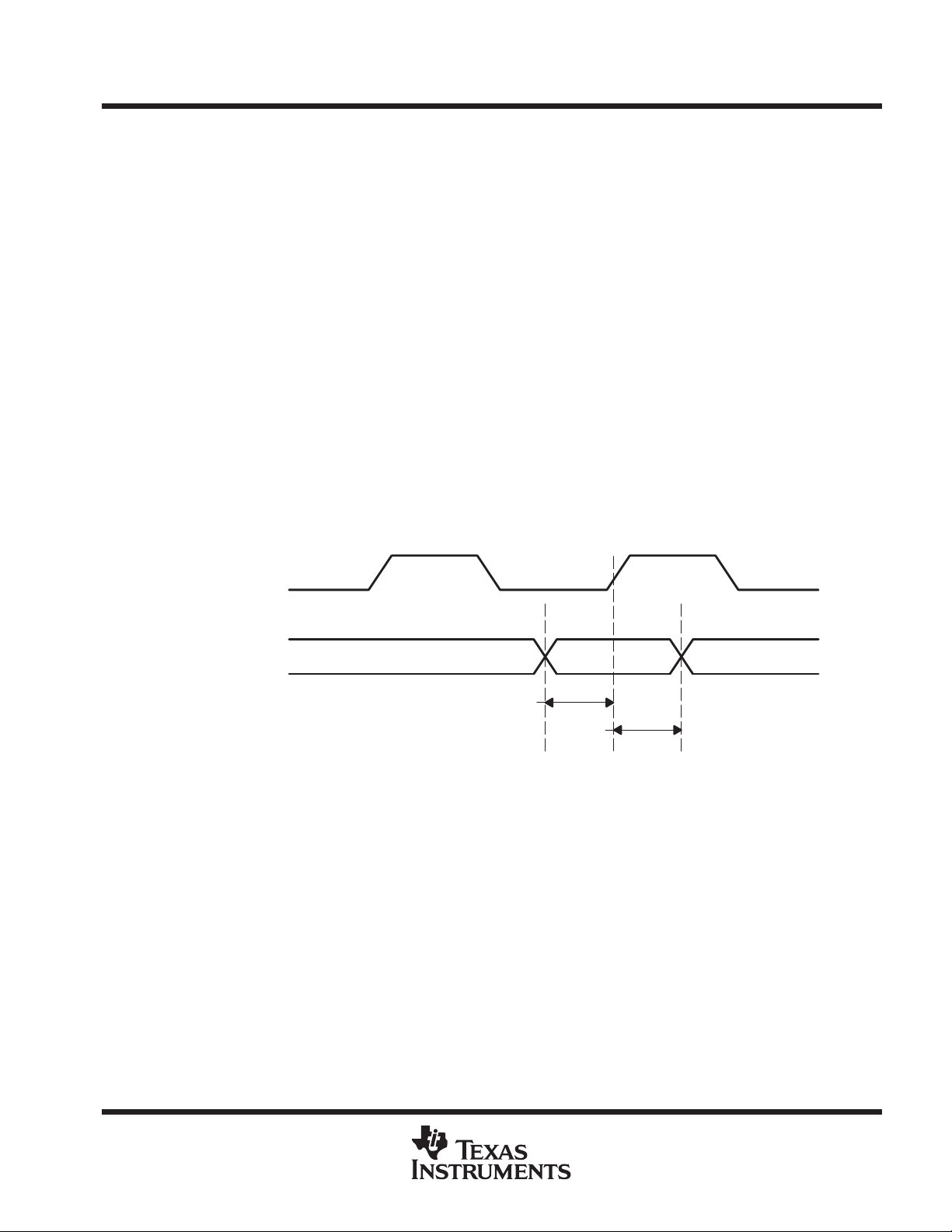
low-speed data bus
The transmit bus interface accepts 16 bit wide single-ended TTL parallel data at the TXD[0–15] pins. Data is
valid on the rising edge of GTX_CLK when TX_EN is asserted high. The GTX_CLK is used as the byte clock.
The data, enable and clock signals must be properly aligned as shown in Figure 1. Detailed timing information
can be found in the TTL input switching characteristics table.
GTX_CLK
TXDn
t
SETUP
t
HOLD
TX_EN, TX_ER
Figure 1. Transmit Timing Waveform
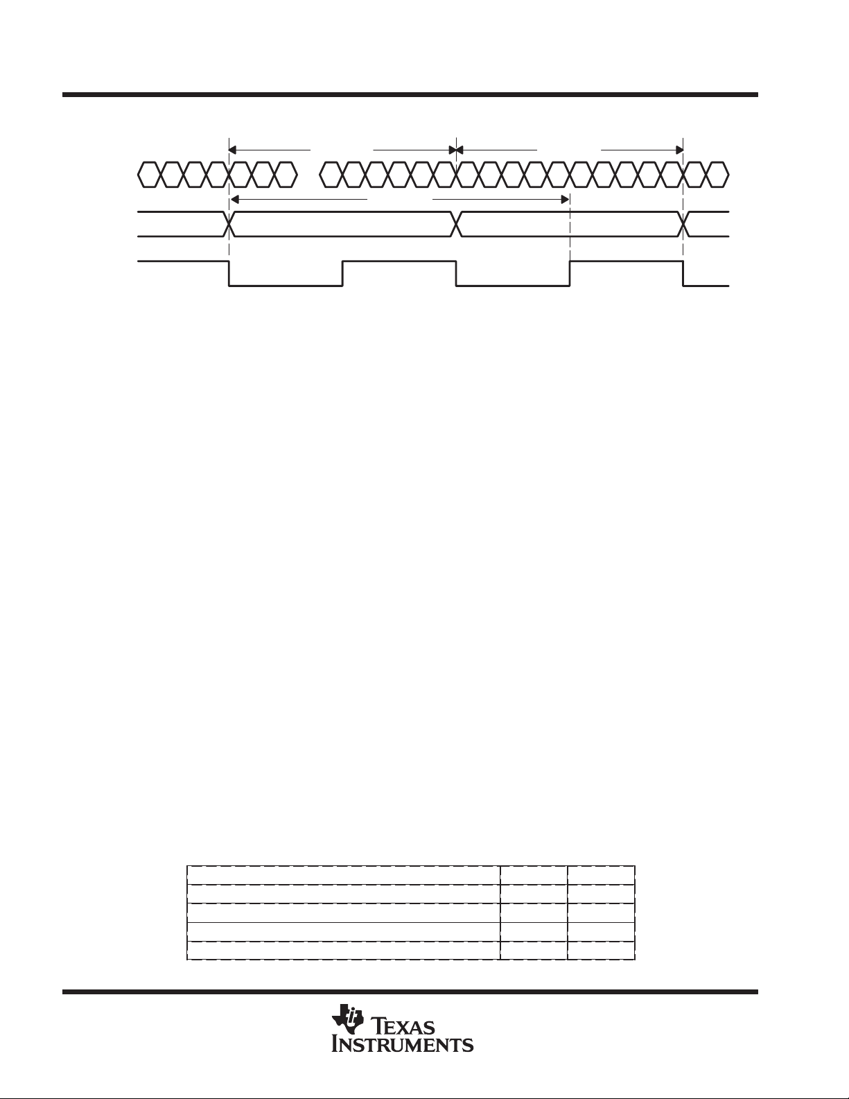
transmission latency
The data transmission latency of the TLK2500 is defined as the delay from the initial 16-bit word load to the serial
transmission of bit 0. The minimum latency is 34 bit times; the maximum is 38 bit times.
Tx Word A Tx Word B
DOUTTXP,
DOUTTXN
T latency
TXD[0–15]
GTX_CLK
†
This figure for illustration only. T
is larger than shown.
latency
Tx Word CTx Word B
Figure 2. Transmitter Latency
POST OFFICE BOX 655303 • DALLAS, TEXAS 75265
3
TLK2500IRCP
1.6 Gbps to 2.5 Gbps TRANSCEIVER
SLLS356B – JUNE 1999 – REVISED JANUARY 2000
transmit interface (continued)
8b/10b encoder
All true serial interfaces require a method of encoding to insure minimum transition density so that the receiving
PLL has a minimal number of transitions in which to stay locked on. The encoding scheme maintains the signal
dc balance by keeping the number of ones and zeros the same. This provides good transition density for clock
recovery and improves error checking. The TLK2500 uses the 8B/10B encoding algorithm that is used by Fibre
channel and gigabit ethernet. This is transparent to the user as the TLK2500 devices internally encode and
decode the data such that the user reads and writes actual 16–bit data.
The 8B/10B encoder converts 8 bit wide data to a 10 bit wide encoded data character to improve its transmission
characteristics. Since the TLK2500 is a 16 bit wide interface the data is split into two 8 bit wide bytes for
encoding. Each byte is fed into a separate encoder. The encoding is dependant upon two additional input
signals, TX_EN and TX_ER. When TX_EN is asserted and TX_ER is deasserted then the data bits TXD[0–15]
are encoded and transmitted normally . When TX_EN is deasserted and TX_ER is asserted, then the encoder
will generate a carrier extend consisting of two K23.7 codes. If TX_EN and TX_ER are both asserted then the
encoder will generate an error event. This error event consists of one or more code-groups that are not part of
the valid data or delimiter set somewhere in the frame being transmitted. Table 1 provides the transmit data
control decoding.
Table 1. Transmit Data Controls
TX_EN TX_ER ENCODED 10 BIT OUTPUT
0 0 IDLE (<K28.5, D5.6>,<K28.5, D16.2>)
0 1 Carrier extend (K23.7)
1 0 Normal data character
1 1 Transmit error propagation (invalid code group)
IDLE generation
The encoder sends the IDLE character set when no payload data is available to be sent and TX_EN/TX_ER
are deasserted. IDLE consists of a K28.5 code and either a D5.6 or D16.2 character. Since data is latched into
the TLK2500 16 bits at a time, this in turn is converted into two 10 bit codes that are transmitted sequentially .
This means IDLE consists of two 10 bit codes, being 20 bits wide that is transmitted during a single GTX_CLK
cycle. IDLE will replace data during initial synchronization or resync, until synchronization is achieved (see
synchronization and initialization).
PRBS generator
The TLK2500 has a pseudo random bit stream (PRBS) function. When the PRBSEN pin is forced high, the
PRBS test is enabled. A PRBS is generated and fed into the 10 bit parallel-to-serial converter input register . Data
from the normal input source is ignored during the PRBS mode. The PRBS pattern is then fed through the
transmit circuitry as if it were normal data and sent out to the transmitter. The output can be sent to a bit error
rate tester (BERT) or to the receiver of another TLK2500. Since the PRBS is not really random but a
predetermined sequence of ones and zeroes the data can be captured and checked for errors by a BERT.
Results are reported on the RX_ER/PRBSPASS pin.
parallel to serial
The parallel-to-serial shift register takes in 10 bit wide data multiplexed from the two 8B/10B encoders and
converts it to a serial stream. The shift register is clocked by the internally generated bit clock, which is 10 × the
GTX_CLK input frequency. The LSB (D0) is transmitted first.
4
POST OFFICE BOX 655303 • DALLAS, TEXAS 75265
TLK2500IRCP
1.6 Gbps to 2.5 Gbps TRANSCEIVER
SLLS356B – JUNE 1999 – REVISED JANUARY 2000
transmit interface (continued)
high-speed data output
The high speed data output driver consists of a differential pair (CML) that can be optimized for a particular
transmission line impedance and length. The line can be directly coupled or ac coupled. The drivers provide
pre-emphasis and de-emphasis. Pre-emphasis is a boost in the serial driver current occurring during a bit
transition (either high-to-low or low-to-high). This current is held for one bit time. De-emphasis is a reduction
in the serial driver current directly following a pre-emphasis event if there is not a transition after the
pre-emphasis event. De-emphasis can be held for multiple bit times if no transition occurs. Refer to Figure 10
and Figure 11 for termination details.
receive interface
The receiver portion of the TLK2500 accepts 8B/10B encoded differential serial data. The interpolator and clock
recovery circuit will lock to the data stream and extract the bit rate clock. This recovered clock is used to retime
the input data stream. The serial data is then aligned to two separate 10-bit word boundaries, 8B/10B decoded
and output on a 16 bit wide parallel bus synchronized to the extracted receive clock.
low-speed data bus
The receive bus interface drives 16 bit wide single-ended TTL parallel data at the RXD[0–15] pins. Data is valid
on the rising edge of RX_CLK when RX_DV is asserted high. The RX_CLK is used as the byte clock. The data,
enable and clock signals must be properly aligned as shown in Figure 3. Detailed timing information can be
found in the TTL output switching characteristics table.
RX_CLK
RXDn, RX_ER, RX_DV
t
SETUP
t
HOLD
Figure 3. Receive Timing Waveform
data reception latency
The serial-to-parallel data latency is the time from when the first bit arrives at the receiver until it is output in the
aligned parallel word with RXD0 received as first bit. The minimum latency is 76 bit times; the maximum is 107
bit times.
POST OFFICE BOX 655303 • DALLAS, TEXAS 75265
5
TLK2500IRCP
1.6 Gbps to 2.5 Gbps TRANSCEIVER
SLLS356B – JUNE 1999 – REVISED JANUARY 2000
receive interface (continued)
Rx Byte B
Rx Byte A
DINRXP,
DINRXN
RXD[1–15]
RX_CLK
†
This figure for illustration only. T
is larger than shown.
latency
Rx Byte A
. . .
T
latency
†
Figure 4. Receiver Latency
serial to parallel
Serial data is received on the DINRXP, DINRXN pins. The interpolator and clock recovery circuit will lock to the
data stream if the clock to be recovered is within ±200 PPM of the internally generated bit rate clock. The
recovered clock is used to retime the input data stream. The serial data is then clocked into the serial-to-parallel
shift registers. The 10 bit wide parallel data is then multiplexed and fed into two separate 8B/10B decoders
where the data is then synchronized to the incoming data steam word boundary by detection of the K28.5
synchronization pattern.
comma detect and 8b/10b decoding
The 8B/10B decoder converts 10 bit encoded data back into 8 bits. The comma detect circuit is designed to
provide for byte synchronization to an 8b/10b transmission code. When parallel data is clocked into a parallel
to serial converter, the byte boundary that was associated with the parallel data is now lost in the serialization
of the data. When the serial data is received and converted to parallel format again a way is needed to be able
to recognize the byte boundary again. Generally this is accomplished through the use of a synchronization
pattern. This is generally a unique a pattern of 1’s and 0’s that either cannot occur as part of valid data or it is
a pattern that repeats at defined intervals. 8b/10b encoding contains a character called the comma (b’001 1111’
or b’1 100000’) which is used by the comma detect circuit to align the received serial data back to its original byte
boundary . The decoder detects the K28.5 comma, generating a synchronization signal aligning the data to their
10 bit boundaries for decoding. It then converts the data back into 8 bit data, removing the control words. The
output from the two decoders are latched into the 16 bit register synchronized to the recovered parallel data
clock (RX_CLK) and valid on the rising edge of RX_CLK.
Rx Byte B
The decoding generates the data bits RXD[0:15] and two additional status signals, RX_DV and RX_ER. When
RX_DV is asserted and RX_ER is deasserted, a valid data word has been received and output on the RXDx
pins. When RX_DV is deasserted and RX_ER is asserted, a carrier extend was received and the data bits are
set to F7F7h. If RX_DV and RX_ER are both asserted, the decoder has either received an error propagation
code (K30.7) or an invalid code. In the former case, the data bits are set to FEFEh. The data bits are set to 0000h
if the received code was invalid. When RX_DV and RX_ER are both deasserted, an IDLE was received and
the data bits are set to either BCC5h or BC50h.
Table 2. Receive Data Controls
RECEIVED ENCODED 10-BIT INPUT RX_DV RX_ER
IDLE (<K28.5, D5.6>,<K28.5, D16.2>) 0 0
Carrier extend (K23.7) 0 1
Normal data character 1 0
Receive error propagation (K30.7) 1 1
6
POST OFFICE BOX 655303 • DALLAS, TEXAS 75265

TLK2500IRCP
1.6 Gbps to 2.5 Gbps TRANSCEIVER
SLLS356B – JUNE 1999 – REVISED JANUARY 2000
receive interface (continued)
synchronization and initialization
The TLK2500 has a synchronization state machine which is responsible for handling link initialization and
synchronization. Upon power up or reset, the state machine enters the acquisition (ACQ) state and searches
for IDLE. Upon receiving 3 consecutive IDLEs or 3 consecutive carrier extends, the state machine will enter the
synchronization (SYNC) state. If the state machine receives valid data or error propagation during the
acquisition process, it will immediately transition to the SYNC state. Loss of synchronization occurs whenever
four consecutive invalid transmissions have been detected or when four invalid transmissions occur prior to
receiving four consecutive valid data groups or IDLEs. A single invalid transmission received while in the SYNC
state will cause the state machine to transition to the loss of synchronization (LOS) state, internally . Receiving
three additional invalid transmissions before four consecutive valid transmissions occur while in LOS will force
the state machine back to the acquisition state. If four consecutive valid transmissions occur, then the state
machine will transition to the SYNC state (see Figures 5 and 6.
prbs verification
The TLK2500 also has a built in BERT function in the receiver side that is enabled by PRBSEN. It can check
for errors and report errors by forcing the RX_ER/PRBSPASS pin low.
Invalid Transmission
Power-Up/Reset
3 Invalid
Transmissions
LOS SYNC
Figure 5. Initialization and Synchronization State Diagram
ACQ
3 Consecutive IDLEs or Carrier Extends,
1 Valid Data or Error Propagation Received
Valid
Transmission
Invalid Transmission
4 Consecutive Valid Transmissions
POST OFFICE BOX 655303 • DALLAS, TEXAS 75265
7

TLK2500IRCP
1.6 Gbps to 2.5 Gbps TRANSCEIVER
SLLS356B – JUNE 1999 – REVISED JANUARY 2000
receive interface (continued)
TX_EN
TX_ER
TXD[1–15]
DOUTTXP,
DOUTTXN
ACQ
xx xx xx xxxxxxxx
xx xx xx xx xx xx xx
xx xxxxxxxx xx xx xx
IDLE
SYNC/LOS
D0–D15
IDLE
D0–D15
Ca. Ext.
Error
Figure 6. State Machine Timing Diagram
reference clock input
The reference clock (GTX_CLK) is an external input clock that synchronizes the transmitter interface. The
reference clock is then multiplied in frequency 10x to produce the internal serialization clock. The internal
serialization clock is frequency-locked to the reference clock and used to clock out the serial transmit data.
operating frequency range
The TLK2500 is optimized for operation at a serial data rate of 2.5 Gbit/s. The TLK2500 may operate at a serial
data rate between 1.6 Gbit/s to 2.5 Gbit/s. GTX_CLK must be within ±100 PPM of the desired parallel data rate
clock.
testability
The TLK2500 has a comprehensive suite of built-in self-tests. The loopback function provides for at-speed
testing of the transmit/receive portions of the circuitry. The enable pin allows for all circuitry to be disabled so
that an Iddq test can be performed. The PRBS function allows for a built-in self test (BIST).
enable function
When held low, the ENABLE pin will disable all quiescent power in both the analog and digital circuitry. This
allows for Iddq testing on all power supplies and can also be used to conserve power when the link is inactive
loop-back testing
The transceiver can provide a self-test function by enabling (LOOPEN) the internal loop-back path. Forcing this
pin high causes serial transmitted data to be routed internally to the receiver. The parallel data output can be
compared to the parallel input data for functional verification. The external differential output is held in a
high-impedance state during the loop-back testing.
built in self test
The TLK2500 has a built-in self test (BIST) function. By combining PRBS with loopback, an effective self–test
of all the circuitry running at full speed can be realized. The successful completion of the BIST is reported on
the RX_ER/PRBS_P ASS pin.
8
POST OFFICE BOX 655303 • DALLAS, TEXAS 75265

TLK2500IRCP
1.6 Gbps to 2.5 Gbps TRANSCEIVER
SLLS356B – JUNE 1999 – REVISED JANUARY 2000
power-on reset
Upon application of minimum valid power, the TLK2500 generates a power-on reset. During the power-on reset
the RXD, RX_ER and RX_DV signal pins are put into a high-impedance state. RX_CLK is held low. The length
of the power-on reset cycle is dependant upon the GTX_CLK frequency but will be less than 1 ms in duration.
pin assignments
RCP PACKAGE
DDA
DDA
V
TXD2
TXD1
TXD0
GNDA
DOUTTXP
DOUTTXN
GNDA
V
RREF
DINRXP
RXD0
DINRXN
GNDA
RXD2
RXD1
V
DD
TXD3
TXD4
TXD5
GND
TXD6
TXD7
GTX_CLK
V
DD
TXD8
TXD9
TXD10
GND
TXD11
TXD12
TXD13
63 62 61 60 5964 58
1
2
3
4
5
6
7
8
9
10
11
12
13
14
15
16
1718 19
GND
TXD14
20
TXD15
21 22 23 24
TX_EN
TX_ER
LOOPEN
56 55 5457
25 26 2728 29
DD
V
ENABLE
LCKREFN
53 52
GND
TESTEN
PRBSEN
51 50 49
30 31 32
RXD15
RX_DV
V
48
RXD3
47
RXD4
46
RXD5
45
RXD6
44
GND
43
RXD7
42
RX_CLK
41
RXD8
40
RXD9
39
V
38
37
RXD10
36
RXD11
35
RXD12
34
RXD13
33
GND
RXD14
DD
DD
RX_ER/PRBS_PASS
POST OFFICE BOX 655303 • DALLAS, TEXAS 75265
9

TLK2500IRCP
I/O
DESCRIPTION
1.6 Gbps to 2.5 Gbps TRANSCEIVER
SLLS356B – JUNE 1999 – REVISED JANUARY 2000
Terminal Functions
TERMINAL
NAME NO.
DINRXP
DINRXN
DOUTTXP
DOUTTXN
ENABLE 24 Input When this pin is held low, the device is disabled for Iddq testing. When high the device operates
GND 5,13,
GNDA 52,58,61Ground Analog ground. GNDA provides a ground reference for the high-speed analog circuits, RX and TX.
54
53
60
59
18,28,
33,43
Input Differential input receive. DINRXP and DINRXN together are the differential serial input interface from a
Output
3-state on
power up
Ground Digital logic ground. Provides a ground for the logic circuits and digital I/O buffers.
copper or an optical I/F module.
Differential output transmit. DOUTTXP and DOUTTXN are differential serial outputs that interface to a
copper or an optical I/F module. These terminals transmit NRZ data at a rate of 20 times the GTX_CLK
value. DOUTTXP and DOUTTXN are put in a high impedance state when LOOPEN is high and are
active when LOOPEN is low . During power-on reset these pins are in a high-impedance state.
normally . Should be tied high.
GTX_CLK 8 Input Reference clock. GTX_CLK is a continuous external input clock that synchronizes the transmitter
LCKREFN 25 Input(with-
LOOPEN 21 Input (with
PRBSEN 26 Input (with
RREF 56 Input The RREF pin is used to connect to an external reference resistor. The other side of the resistor is
RXD0
RXD1
RXD2
RXD3
RXD4
RXD5
RXD6
RXD7
RXD8
RXD9
RXD10
RXD11
RXD12
RXD13
RXD14
RXD15
RX_CLK 41 Output
51
50
49
47
46
45
44
42
40
39
37
36
35
34
32
31
pullup)
pulldown)
pulldown
Output
(3-state on
powerup)
(low on
powerup)
interface signals TX_EN, TX_ER and TXD. The frequency range of GTX_CLK is 80 MHz to 125 MHz.
The transmitter uses the rising edge of this clock to register the 16-bit input data (TDX) for serialization.
Lock to reference. When low the receiver clock is frequency locked to REFCLK but may contain a phase
offset from REFCLK and the synchronization state machine is bypassed. This places the device in a
transmit only mode since the receiver is not tracking the data. When high the receiver is locked to the
received data stream and must receive valid codes from the synchronization state machine before the
transmitter is enabled.
Loop enable. When LOOPEN is high (active), the internal loop-back path is activated. The transmitted
serial data is directly routed to the inputs of the receiver. This provides a self-test capability in
conjunction with the protocol device. The DOUTTXP and DOUTTXN outputs are held in a high
impedance state during the loop-back test. LOOPEN is held low during standard operational state with
external serial outputs and inputs active.
Enables the PRBS test. When high results of test can be monitored on the RX_ER/PRBS_P ASS pin. A
high on PRBS_PASS indicates that valid PRBS is being received. Should be tied low.
connected to analog VDD. The resistor is used to provide an accurate current reference to the
transmitter I/O circuitry.
Receive data. These outputs carry 16–bit parallel data output from the transceiver to the Controller,
synchronized to RX_CLK. The data is valid on the rising edge of RX_CLK as shown in Figure 3. These
pins are in a high-impedance state during power-on reset.
Output clock that is synchronized to RXD, RX_ER, RX_DV . RX_CLK is the recovered serial data rate
clock divided by 20. RX_CLK is held low during power-on reset.
10
POST OFFICE BOX 655303 • DALLAS, TEXAS 75265

I/O
DESCRIPTION
TERMINAL
NAME NO.
RX_ER/
PRBS_PASS
RX_DV 30 Output
TESTEN 27 Input (with
TXD0
TXD1
TXD2
TXD3
TXD4
TXD5
TXD6
TXD7
TXD8
TXD9
TXD10
TXD11
TXD12
TXD13
TXD14
TXD15
TX_EN 20 Input ( with
TX_ER 22 Input (with
V
DD
V
DDA
29 Output
(3-state on
powerup)
3-state on
power up
pulldown)
62
63
64
2
3
4
6
7
10
11
12
14
15
16
17
19
1,9,23,
38,48
55,57 Supply Analog power. V
Input Transmit data. These inputs carry the 16-bit parallel data output from a protocol device to the transceiver
pulldown)
pulldown)
Supply Digital logic power. Provides power for all digital circuitry and digital I/O buffers.
TLK2500IRCP
1.6 Gbps to 2.5 Gbps TRANSCEIVER
SLLS356B – JUNE 1999 – REVISED JANUARY 2000
Terminal Functions(Continued)
Receive error. Controlled by PRBSEN pin. When PRBSEN= low then pin is used to indicate receive
error (RX_ER). When PRBSEN is high then pin indicates status of the PRBS test results (High=pass).
RX_ER is in a high-impedance state during power-on reset.
When RX_ER and RX_DV are asserted, indicates that an error was detected somewhere in the frame
presently being transferred from the PHY. When RX_ER is asserted and RX_DV is deasserted,
indicates that carrier extend data is being presented.
Receive data valid. RX_DV is driven by the PHY to indicate that the PHY is presenting recovered and
decoded data on RXD. RX_DV shall be asserted continuously from the first recovered doublet of the
frame through the final recovered doublet and shall be negated prior to the first rising edge of RX_CLK
that follows the final doublet. RX_DV is in a high-impedance state during power-on reset.
Test mode enable, should be tied low.
for encoding, serialization and transmission. This 16-bit parallel data is clocked into the transceiver on
the rising edge of GTX_CLK.
Transmit enable. TX_EN in combination with TX_ER indicates the controller is presenting data on the
parallel for transmission. TX_EN shall be high with the first doublet of the preamble and remain asserted
while all doublet to be transmitted are presented. TX_EN shall be negated prior to the first rising edge of
GTX_CLK following the final doublet of a frame.
Transmit error coding. When TX_ER and TX_EN are high, indicates that the PHY will generate an error
somewhere in the frame presently being transferred. When TX_ER is asserted and TX_EN is
deasserted, indicates the controller is presenting carrier extension data. When TX_ER is deasserted
with TX_EN asserted, indicates that normal data is being presented.
provides a supply reference for the high-speed analog circuits, receiver and
transmitter
DDA
POST OFFICE BOX 655303 • DALLAS, TEXAS 75265
11

TLK2500IRCP
ICCSupply current
mA
RωFrequenc
MH
1.6 Gbps to 2.5 Gbps TRANSCEIVER
SLLS356B – JUNE 1999 – REVISED JANUARY 2000
absolute maximum ratings over operating free-air temperature (unless otherwise noted)
†
Supply voltage, VDD (see Note 1) –0.3 V to 3 V. . . . . . . . . . . . . . . . . . . . . . . . . . . . . . . . . . . . . . . . . . . . . . . . . . . . . .
Voltage range: TxD, ENABLE, GTX_CLK, TX_EN, TX_ER, LOOPEN, PRBS_EN –0.3 V to 4 V. . . . . . . . . . .
Any other terminal except above –0.3 V to VCC + 0.3 V. . . . . . . . . . . . . . . . . . . . . . . . . . . . . . . . .
Package power dissipation rating See Dissipation Rating Table. . . . . . . . . . . . . . . . . . . . . . . . . . . . . . . . . . . . . . . .
Electrostatic discharge Class 1, A:500 V,. . . . . . . . . . . . . . . . . . . . . . . . . . . . . . . . . . . . . . . . . . . . . . . . . . . . . . . . . . .
Class 1, B:50 V
Characterized free-air operating temperature range –40°C to 85°C. . . . . . . . . . . . . . . . . . . . . . . . . . . . . . . . . . . . .
Storage temperature range –65°C to 150°C. . . . . . . . . . . . . . . . . . . . . . . . . . . . . . . . . . . . . . . . . . . . . . . . . . . . . . . .
Lead temperature 1,6 mm (1/16 inch) from case for 10 seconds 260°C. . . . . . . . . . . . . . . . . . . . . . . . . . . . . . . . .
†
Stresses beyond those listed under “absolute maximum ratings” may cause permanent damage to the device. These are stress ratings only, and
functional operation of the device at these or any other conditions beyond those indicated under “recommended operating conditions” is not
implied. Exposure to absolute-maximum-rated conditions for extended periods may affect device reliability.
NOTE 1: All voltage values, except differential I/O bus voltages, are with respect to network ground.
DISSIPATION RATING TABLE
PACKAGE
‡
RCP64
§
RCP64
¶
RCP64
†
This is the inverse of the traditional junction-to-ambient thermal resistance (R
‡
2 oz. Trace and copper pad with solder.
§
2 oz. Trace and copper pad without solder.
¶
Standard JEDEC high-K board. For more information, refer to TI application note
Thermally Enhanced Package,
TA ≤ 25°C
POWER RATING
5.25 W 46.58 mW/°C 2.89 W
3.17 W 23.70mW/°C 1.74 W
2.01 W 13.19 mW/°C 1.11 W
TI literature number SLMA002.
DERATING FACTOR
ABOVE TA = 25°C
†
POWER RATING
TA = 70°C
).
qJA
PowerPAD
electrical characteristics over recommended operating conditions
PARAMETER TEST CONDITIONS MIN NOM MAX UNIT
V
DD
P
D
PLL
DATA
T
A
(LCK)
(LCK)
Supply voltage 2.3 2.5 2.7 V
pp
Power dissipation
Shutdown current Enable = 0, V
PLL lock time VDD/V
DATA lock time After PLL lock 1024
Free–air temperature –40 85 °C
VDD = 2.5 V, Frequency = 1.5 Gbps, PRBS pattern 95
VDD = 2.5 V, Frequency = 2.5 Gbps, PRBS pattern 135
VDD = 2.5 V, Frequency = 1.5 Gbps, PRBS pattern 238
VDD = 2.5 V,
VDD = max, Frequency = 2.5 Gbps, Worstcase pattern 461
DDC
Frequency = 2.5 Gbps, PRBS pattern 337
, VDD pins, VDD = maximum 20 µA
DDA
= minimum 0.1 0.4 ms
mW
bit
times
reference clock (GTX_CLK) timing requirements over recommended operating conditions (unless
otherwise noted)
PARAMETER TEST CONDITIONS MIN TYP MAX UNIT
y
Frequency tolerance –100 100 ppm
Duty cycle 40% 50% 60%
Peak-to-peak jitter 40 ps
Minimum data rate TYP–0.01% 80 TYP+0.01%
Maximum data rate
TYP–0.01% 125 TYP+0.01%
z
12
POST OFFICE BOX 655303 • DALLAS, TEXAS 75265

0.8 to 2 V
C 5 F,
V/ns
t
RXD, RX_DV, RX_ER setup to ↑ RX_CLK
ns
t
hold
RXD, RX_DV, RX_ER hold to ↑ RX_CLK
ns
TLK2500IRCP
1.6 Gbps to 2.5 Gbps TRANSCEIVER
SLLS356B – JUNE 1999 – REVISED JANUARY 2000
TTL input electrical characteristics over recommended operating conditions, TTL signals:
TXD0–TXD15, GTX_CLK, LOOPEN, LCKREFN (unless otherwise noted)
PARAMETER TEST CONDITIONS MIN NOM MAX UNIT
V
IH
V
IL
I
IH
I
IL
C
I
t
r
t
f
t
setup
t
hold
TTL output switching characteristics over recommended operating conditions (unless otherwise
noted)
V
OH
V
OL
SR
SR
setup
High-level input voltage See Figure 7 2 3.6 V
Low-level input voltage See Figure 7 0.80 V
Input high current VDD = MAX, VIN = 2 V 40 µA
Input low current VDD = MAX, VIN = 0.4 V –600 µA
Input capacitance 4 pF
Rise time, GTX_CLK, TX_EN, TX_ER, TXD 0.8 V to 2 V, C = 5 pF, See Figure 7 1 ns
Fall time, GTX_CLK, TX_EN, TX_ER, TXD 2 V to 0.8 V, C = 5 pF, See Figure 7 1 ns
TXD, TX_EN, TX_ER setup to ↑GTX_CLK See Figure 7 1.5 ns
TXD, TX_EN, TX_ER hold to ↑GTX_CLK See Figure 7 0.4 ns
PARAMETER TEST CONDITIONS MIN NOM MAX UNIT
High-level output voltage IOH = –1 mA, VDD = MIN 2.10 2.3 V
Low-level output voltage IOH = 1 mA, VDD = MIN GND 0.25 0.5 V
Magnitude of RX_CLK, RX_ER, RX_DV , RXD slew rate
(r)
(rising)
Magnitude of RX_CLK, RX_ER, RX_DV , RXD slew rate
(f)
(falling)
p
,
50%, 80 MHz, See Figure 7 5.4
50%, 125 MHz, See Figure 7 3
50%, 80 MHz, See Figure 7 5.4
50%, 125 MHz, See Figure 7 3
C = 5 pF,
See Figure 7
0.5
0.5
RX_CLK
GTX_CLK
TX_ER, TX_EN, TXD
RX_ER, RX_DV , RXD
Figure 7. TTL Data Input/Output Valid Levels for AC Measurements
t
SETUP
t
HOLD
2 V
0.8 V
2 V
0.8 V
POST OFFICE BOX 655303 • DALLAS, TEXAS 75265
13

TLK2500IRCP
,
,
R
T
Ω,
R
REF
200 Ω,
t
Serial data total jitter (peak-to-peak)
UI
1.6 Gbps to 2.5 Gbps TRANSCEIVER
SLLS356B – JUNE 1999 – REVISED JANUARY 2000
transmitter/receiver characteristics
PARAMETER TEST CONDITIONS MIN TYP MAX UNIT
V
(odp)
V
(odd)
V
ICR
V
ID
V
ICR
I
lkg
C
I
(TOT)
tr, t
J
(t)
Pre-emphasis VOD,direct, |VTx+–VTx–|
De-emphasis VOD, direct, |VTx+–VTx–|
Transmit common mode voltage range 1500 2500 mV
Receiver input voltage requirement,
|Rx+ – Rx–|
Receiver common mode voltage range
(VTx + + VTx–)/2
Receiver input leakage current –10 10 µA
Receiver input capacitance 2 pF
p
p
Differential signal rise, fall time (20% to 80%) RL = 50 Ω, CL = 5 pF, See Figure 8 100 150 ps
f
Jitter tolerance Zero crossing 50% UI
DOUTTXP
R
= 50 Ω
50
DC Coupled
Differential output jitter at 2.5 Gbps 0.16
Differential output jitter at 1.5 Gbps 0.2
t
r
R
See Figure 8
t
f
= 200 Ω
80%
50%
20%
840 1050 1260 mV
760 950 1140 mV
200 mV
1500 mV
DOUTTXN
Figure 8. Differential and Common-Mode Output Voltage Definitions
thermal characteristics
PARAMETER TEST CONDITION MIN TYP MAX UNIT
R
R
Junction-to-free-air thermal resistance
θJA
Junction-to-case-thermal resistance
θJC
80%
50%
20%
t
80%
V
OD
20%
Board mounted, no air flow, high conductivity TI
recommended test board, chip soldered or greased
to thermal land
Board mounted, no air flow, high conductivity TI
recommended test board with thermal land but no
solder or grease thermal connection to thermal land
Board mounted, no air flow, JEDEC test board 75.83
Board mounted, no air flow, high conductivity TI
recommended test board, chip soldered or greased
to thermal land
Board mounted, no air flow, high conductivity TI
recommended test board with thermal land but no
solder or grease thermal connection to thermal land
Board mounted, no air flow, JEDEC test board 7.8
t
r
f
+V
0 V
–V
t
t
r
f
21.47
°C/W
42.20
0.38
°C/W
0.38
14
POST OFFICE BOX 655303 • DALLAS, TEXAS 75265

Rt
Termination resistor
Ω
RREF
Reference resistor
Ω
TLK2500IRCP
1.6 Gbps to 2.5 Gbps TRANSCEIVER
SLLS356B – JUNE 1999 – REVISED JANUARY 2000
APPLICATION INFORMATION
V
DD
V
DD
0.01 µF
0.01 µF
R
0.01 µF
Analog/Digital
Isolation
0.01 µF
t
1 nF – 10 nF
5 Ω @ 100 MHz
200 Ω
V
t
810 Ω
TXD3
TXD4
TXD5
TXD6
TXD7
V
DD
TXD8
TXD9
TXD10
TXD11
TXD12
TXD13
V
DDA
R
t
TXD0
TXD2
TXD1
63 62 61 60 5964 58
V
1
DD
2
3
4
5
GND
6
7
8
GTX_CLK
9
10
11
12
GND
13
14
15
16
1718 19
20
R
t
GNDA
DOUTTXP
DOUTTXN
21 22 23 24
1 nF – 10 nF
0.01 µF
0.01 µF
56 55 5457
DDA
RREF
GNDA
V
DD
V
LCKREFN
ENABLE
25 26 2728 29
RREF
DDA
V
R
t
53 52
DINRXP
DINRXN
V
t
R
RXD0
51 50 49
GNDA
30 31 32
t
RXD1
DXD2
48
47
46
45
44
43
42
41
40
39
38
37
36
35
34
33
V
DD
RXD3
RXD4
RXD5
RXD6
GND
RXD7
RX_CLK
RXD8
RXD9
VDD
RXD10
RXD11
RXD12
RXD13
GND
GND
TXD14
Recommend each VDD and GND pair decoupled
with 0.01 µF and 100 pF as close to chip as
possible.
V
DD
Figure 9. External Component Interconnection
recommended values of external resistors
PARAMETER TEST CONDITIONS MIN TYP MAX UNIT
POST OFFICE BOX 655303 • DALLAS, TEXAS 75265
TXD15
TX_EN
TX_ER
LOOPEN
4.7 kΩ
GND
TESTEN
PRBSEN
4.7 kΩ
50 Ω environment 48 50 52
75 Ω environment 71 75 79
50 Ω environment 190 200 210
75 Ω environment 285 300 315
RX_ER/PRBS_PASS
RXD15
RX_DV
RXD14
15

TLK2500IRCP
1.6 Gbps to 2.5 Gbps TRANSCEIVER
SLLS356B – JUNE 1999 – REVISED JANUARY 2000
APPLICATION INFORMATION
choosing resistor values
TLK2500 offers the flexibility to customize the voltage swing and transmission line termination by adjusting the
reference resistor (RREF) and termination resistor (Rt). By choosing particular resistor values, the system can
be optimized for a particular transmission line impedance and length as well as for controlling the output swing
for EMI and attenuation concerns. Refer to the following equations to determine the nominal voltage swing and
driver current as a function of resistor values.
I (de-emphasis in ma) = 3.8 V/RREF
I (pre-emphasis in ma) = 4.2 V/RREF
Vod(de-emphasis in mV) = Rt × 3.8 V/RREF (Direct coupled mode)
Vod(pre-emphasis in mV) = Rt ×4.2 V/RREF (Direct coupled mode)
Vod(de-emphasis in mV) = Rt ×1.9 V/RREF (A/C coupled mode)
Vod(pre-emphasis in mV) = Rt ×2.1 V/RREF (A/C coupled mode)
HIGH SPEED I/O DIRECTLY COUPLED MODE
TXP
TXN
DataData
Pre-Emphasis = 21 mA
De-Emphasis = 19 mA
V
R
t
V
R
t
TERM
TERM
RXP
+
_
RXN
16
TRANSMITTER MEDIA RECEIVER
Figure 10. High Speed I/O Directly Coupled Mode
POST OFFICE BOX 655303 • DALLAS, TEXAS 75265

TLK2500IRCP
1.6 Gbps to 2.5 Gbps TRANSCEIVER
SLLS356B – JUNE 1999 – REVISED JANUARY 2000
APPLICATION INFORMATION
HIGH SPEED I/O A/C-COUPLED MODE
TXP
TXN
DataData
Pre-Emphasis = 21 mA
De-Emphasis = 19 mA
V
CC
R
t
V
CC
0.01 µF
R
t
0.01 µF
V
CC
200
820
V
TERM
R
V
TERM
R
V
TERM
t
t
RXP
+
_
RXN
TRANSMITTER MEDIA RECEIVER
Figure 11. High Speed I/O AC Coupled Mode
designing with PowerPAD
The TLK2500 is housed in a high-performance, thermally enhanced, 64-pin VQFP (RCP64) PowerPAD
package. Use of the PowerPAD package does not require any special considerations except to note that the
PowerPAD, which is an exposed die pad on the bottom of the device, is a metallic thermal and electrical
conductor. Therefore, if not implementing PowerP AD PCB features, the use of solder masks (or other assembly
techniques) may be required to prevent any inadvertent shorting by the exposed PowerPAD of connection
etches or vias under the package. It is strongly recommended that the PowerP AD be soldered to the thermal
land. The recommended convention, however, is to not run any etches or signal vias under the device, but to
have only a grounded thermal land as explained below. Although the actual size of the exposed die pad may
vary , the minimum size required for the keepout area for the 64-pin PFP PowerPAD package is 8 mm × 8 mm.
POST OFFICE BOX 655303 • DALLAS, TEXAS 75265
17

TLK2500IRCP
1.6 Gbps to 2.5 Gbps TRANSCEIVER
SLLS356B – JUNE 1999 – REVISED JANUARY 2000
APPLICATION INFORMATION
designing with PowerPAD (continued)
It is recommended that there be a thermal land, which is an area of solder-tinned copper, underneath the
PowerP AD package. The thermal land will vary in size depending on the PowerPAD package being used, the
PCB construction, and the amount of heat that needs to be removed. In addition, the thermal land may or may
not contain numerous thermal vias depending on PCB construction.
Other requirements for thermal lands and thermal vias are detailed in the TI application note
Thermally Enhanced Package Application Report
pages beginning at URL: http://www.ti.com.
Figure 12. Example of a Thermal Land
For the TLK2500, this thermal land should be grounded to the low impedance ground plane of the device. This
improves not only thermal performance but also the electrical grounding of the device. It is also recommended
that the device ground pin landing pads be connected directly to the grounded thermal land. The land size
should be as large as possible without shorting device signal pins. The thermal land may be soldered to the
exposed PowerPAD using standard reflow soldering techniques.
While the thermal land may be electrically floated and configured to remove heat to an external heat sink, it is
recommended that the thermal land be connected to the low impedance ground plane for the device. More
information may be obtained from the TI application note
, TI literature number SLMA002, available via the TI Web
PHY Layout
, TI literature number SLLA020.
PowerPAD
18
POST OFFICE BOX 655303 • DALLAS, TEXAS 75265

TLK2500IRCP
1.6 Gbps to 2.5 Gbps TRANSCEIVER
SLLS356B – JUNE 1999 – REVISED JANUARY 2000
MECHANICAL DATA
RCP (S-PQFP-G64) PowerPAD PLASTIC QUAD FLATPACK
Definitions
0,50
48
0,27
0,17
33
0,08
M
49
64
0,85
0,75
1,00 MAX
32
Thermal Pad
(See Note D)
17
0,13 NOM
1
7,50 TYP
10,20
SQ
9,80
12,20
SQ
11,80
16
0,15
0,05
Seating Plane
0,08
Gage Plane
0,25
0° – 7°
0,75
0,45
NOTES: A. All linear dimensions are in millimeters.
B. This drawing is subject to change without notice.
C. Body dimensions do not include mold flash or protrusion.
D. The package thermal performance may be enhanced by bonding the thermal pad to an external thermal plane.
This pad is electrically and thermally connected to the backside of the die and possibly selected leads.
E. Falls within JEDEC MS-026
PowerPAD is a trademark of Texas Instruments Incorporated.
POST OFFICE BOX 655303 • DALLAS, TEXAS 75265
4147711/A 10/98
19

IMPORTANT NOTICE
T exas Instruments and its subsidiaries (TI) reserve the right to make changes to their products or to discontinue
any product or service without notice, and advise customers to obtain the latest version of relevant information
to verify, before placing orders, that information being relied on is current and complete. All products are sold
subject to the terms and conditions of sale supplied at the time of order acknowledgement, including those
pertaining to warranty, patent infringement, and limitation of liability.
TI warrants performance of its semiconductor products to the specifications applicable at the time of sale in
accordance with TI’s standard warranty. Testing and other quality control techniques are utilized to the extent
TI deems necessary to support this warranty . Specific testing of all parameters of each device is not necessarily
performed, except those mandated by government requirements.
CERTAIN APPLICATIONS USING SEMICONDUCTOR PRODUCTS MAY INVOLVE POTENTIAL RISKS OF
DEATH, PERSONAL INJURY, OR SEVERE PROPERTY OR ENVIRONMENTAL DAMAGE (“CRITICAL
APPLICATIONS”). TI SEMICONDUCTOR PRODUCTS ARE NOT DESIGNED, AUTHORIZED, OR
WARRANTED TO BE SUITABLE FOR USE IN LIFE-SUPPORT DEVICES OR SYSTEMS OR OTHER
CRITICAL APPLICA TIONS. INCLUSION OF TI PRODUCTS IN SUCH APPLICATIONS IS UNDERST OOD TO
BE FULLY AT THE CUSTOMER’S RISK.
In order to minimize risks associated with the customer’s applications, adequate design and operating
safeguards must be provided by the customer to minimize inherent or procedural hazards.
TI assumes no liability for applications assistance or customer product design. TI does not warrant or represent
that any license, either express or implied, is granted under any patent right, copyright, mask work right, or other
intellectual property right of TI covering or relating to any combination, machine, or process in which such
semiconductor products or services might be or are used. TI’s publication of information regarding any third
party’s products or services does not constitute TI’s approval, warranty or endorsement thereof.
Copyright 2000, Texas Instruments Incorporated
 Loading...