

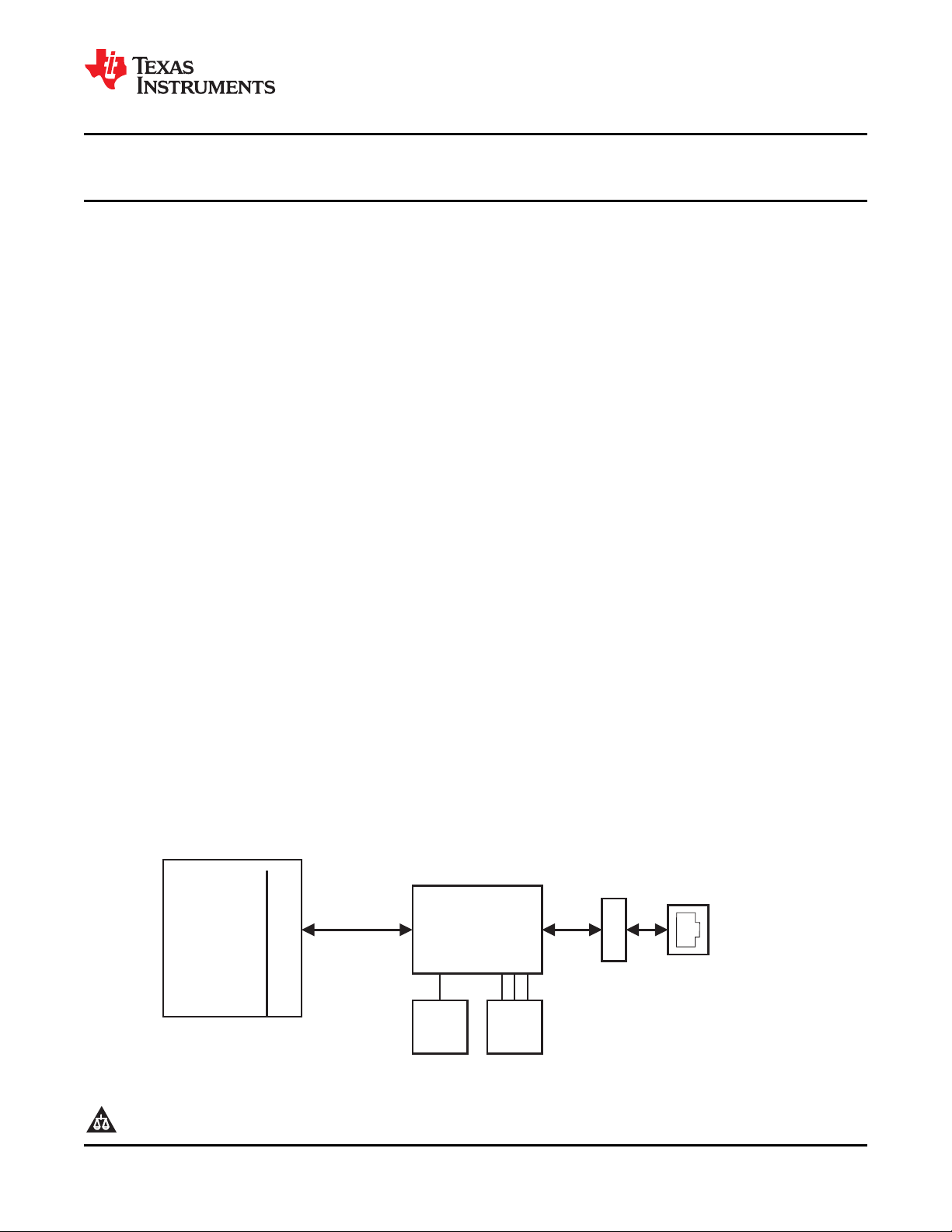
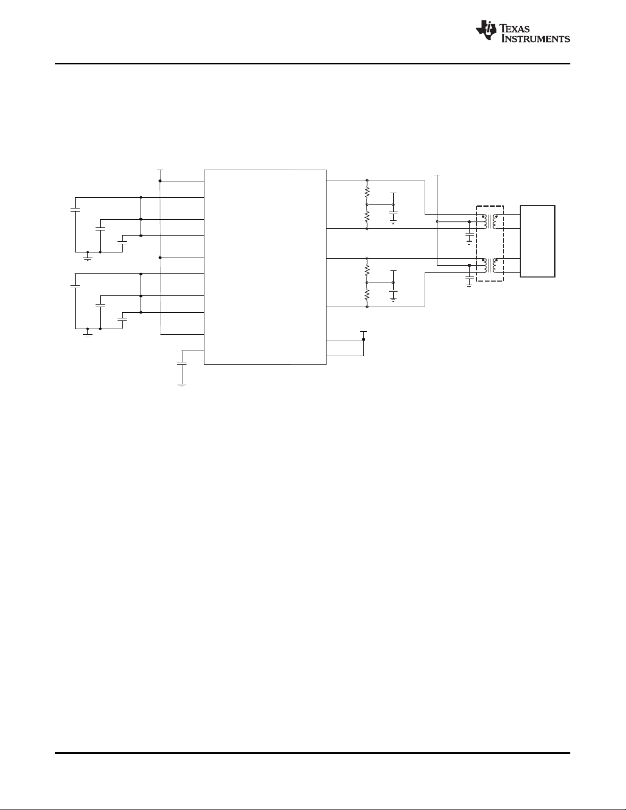
Magnetics
MPU/CPU
Media AccessController
MII
10/100Mb/s
TLK100
25-MHz
Clock
Source
Status
LEDs
RJ-45
10BASE-T
or
100BASE-TX
B0312-01
TLK100
www.ti.com
SLLS931–AUGUST 2009
Industrial Temp, Single Port 10/100 Mb/s Ethernet Physical Layer Transceiver
Check for Samples: TLK100
1 Introduction
1.1 Features
1
• Temperature From –40°C to 85°C
• Low Power Consumption, < 200mW Typical
• Cable Diagnostics
• Error-free Operation up to 200 meters under
typical conditions • Integrated ANSI X3.263 Compliant TP-PMD
• 3.3V MAC Interface
• Auto-MDIX for 10/100 Mb/s
• Energy Detection Mode
• 25 MHz Clock Out
• MII Serial Management Interface (MDC and
MDIO)
• IEEE 802.3u MII
• IEEE 802.3u Auto-Negotiation and Parallel
Detection
• IEEE 802.3u ENDEC, 10BASE-T
Transceivers and Filters
• Bus I/O Protection - ±16kV JEDEC HBM
• IEEE 802.3u PCS, 100BASE-TX Transceivers
• IEEE 1149.1 JTAG
Physical Sublayer with Adaptive Equalization
and Baseline Wander Compensation
• Programmable LED Support Link, 10/100 Mb/s
Mode, Activity, and Collision Detect
• 10/100 Mb/s Packet BIST (Built in Self Test)
• 48-pin TQFP Package (7mm) × (7mm)
1.2 Applications
• Industrial Controls and Factory Automation
• General Embedded Applications
1.3 General Description
The TLK100 is a single-port Ethernet PHY for 10BaseT and 100Base TX signaling. It integrates all the
physical-layer functions needed to transmit and receive data on standard twisted-pair cables. This device
supports the standard Media Independent Interface (MII) for direct connection to a Media Access
Controller (MAC).
The TLK100 is designed for power-supply flexibility, and can operate with a single 3.3V power supply or
with combinations of 3.3V, 1.8V, and 1.1V power supplies for reduced power operation.
The TLK100 uses mixed-signal processing to perform equalization, data recovery, and error correction to
achieve robust operation over CAT 5 twisted-pair wiring. It not only meets the requirements of IEEE 802.3,
but maintains high margins in terms of cross-talk and alien noise.
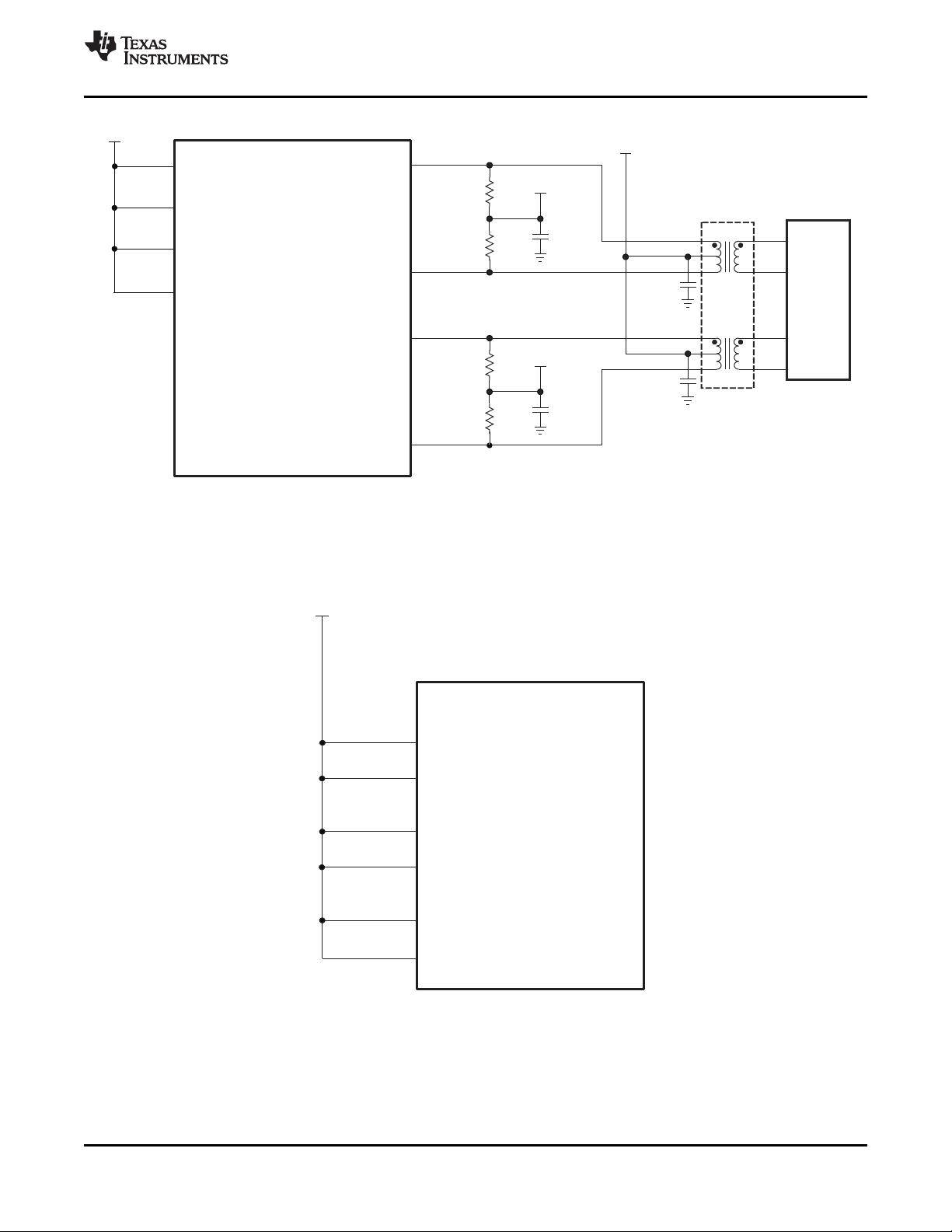
1.4 System Diagram
1
Please be aware that an important notice concerning availability, standard warranty, and use in critical applications of Texas
Instruments semiconductor products and disclaimers thereto appears at the end of this data sheet.
PRODUCTION DATA information is current as of publication date.
Products conform to specifications per the terms of the Texas
Instruments standard warranty. Production processing does not
necessarily include testingof all parameters.
Copyright © 2009, Texas Instruments Incorporated
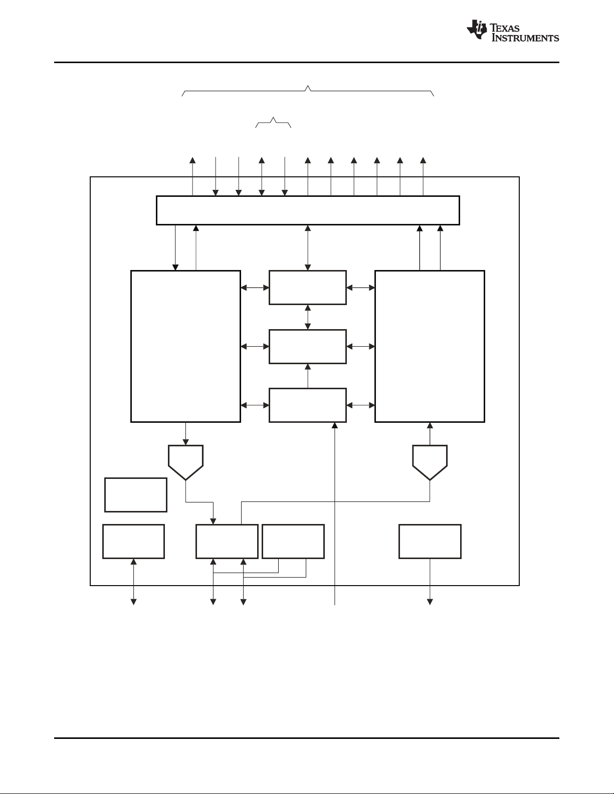
TX_CLK
TXD[3:0]
TX_EN
MDIO
MDC
COL
CRS/CRS_DV
RX_ER
RX_DV
RXD[3:0]
RX_CLK
TX_DATA RX_CLK
Reference Clock
TD± RD± LEDs
MII Interface
Auto-MDIX
DAC ADC
JTAG
MII
Serial
Management
TX_CLK RX_DATA
10BASE-T
and
100BASE-TX
10BASE-T
and
100BASE-TX
Transmit
Block
Receive
Block
MII
Registers
Auto-Negotiation
StateMachine
Clock
Generation
Boundary
Scan
LED
Drivers
B0313-01
Cable
Diagnostics
BIST
TLK100
SLLS931–AUGUST 2009
www.ti.com
Figure 1-1. TLK100 Functional Block Diagram
2 Introduction Copyright © 2009, Texas Instruments Incorporated
Submit Documentation Feedback
Product Folder Link(s): TLK100
VSS
4
8
4
7
4
6
4
5
4
4
4
3
4
2
4
1
4
0
3
9
3
8
3
7
1
2
1
1
109
8
7
6
5
4
3
2
1
1
3
1
4
1
5
1
6
1
7
1
8
1
9
2
0
2
1
2
2
2
3
2
4
2
5
2
6
2
7
2
8
2
9
3
0
3
1
3
2
3
3
3
4
3
5
3
6
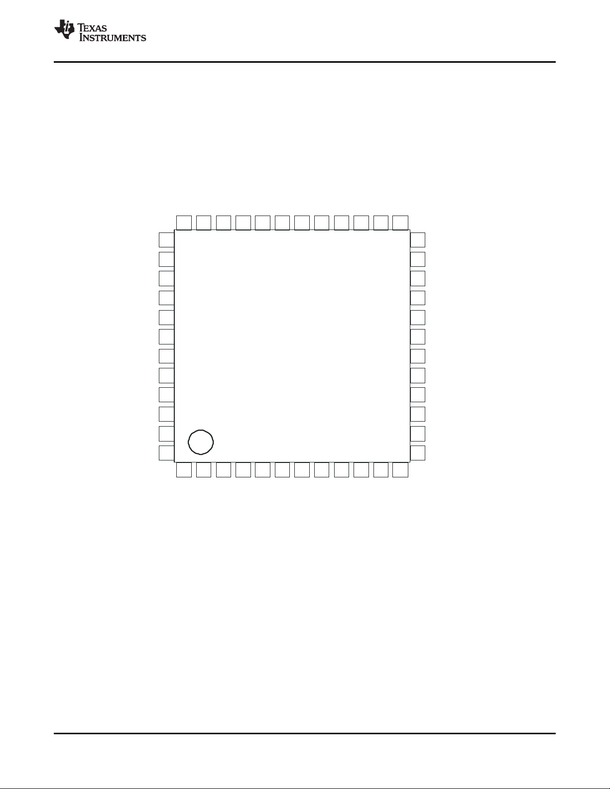
TLK100
RBIAS
CLK25OUT
MII_TXD_0
MII_TXD_1
MII_TXD_2
MII_TXD_3
MII_RX_CLK
MII_CRS / LED_CFG
MII_TX_EN
MII_TX_CLK
MII_COL / PHYAD0
MII_RX_DV
MII_RXD_0 / PHYAD1
MII_RXD_1 / PHYAD2
MII_RXD_2 / PHYAD3
MII_RXD_3 / PHYAD4
MDC
MDIO
LED_ACT / AN_EN
LED_SPEED/ AN_1
LED_LINK / AN_0
PWRDNN/INT
RESETN
JTAG_TCK
JTAG_TDI
JTAG_TMS
JTAG_TDO
JTAG_TRSTN
XO
MII_RX_ERR / MDIX_EN
TD-
TD+
RD-
RD+
VA11_PFBOUT
V18_PFBOUT
VA11_PFBIN1
VA11_PFBIN2
V18_PFBIN1
V18_PFBIN2
VDD33_ VA11
VDD11
VDD33_IO
VDD33_IO
VDD33_V18
VDD33_VD11
XI
TLK100
www.ti.com
1.5 Pin Layout
SLLS931–AUGUST 2009
Figure 1-2. TLK100 PIN DIAGRAM, TOP VIEW
Copyright © 2009, Texas Instruments Incorporated Introduction 3
Submit Documentation Feedback
Product Folder Link(s): TLK100

TLK100
SLLS931–AUGUST 2009
www.ti.com
Contents
1 Introduction .............................................. 1 3.7 Cable Diagnostics .................................. 19
1.1 Features .............................................. 1
1.2 Applications .......................................... 1
1.3 General Description .................................. 1
1.4 System Diagram ..................................... 1
1.5 Pin Layout ............................................ 3
2 Pin Descriptions ......................................... 5
2.1 Serial Management Interface ........................ 5
2.2 MAC Data Interface .................................. 6
2.3 Clock Interface ....................................... 6
2.4 LED Interface ........................................ 6
2.5 JTAG Interface ....................................... 7
2.6 Reset and Power Down .............................. 7
2.7 Jumper Options ...................................... 8
2.8 10 Mb/s and 100 Mb/s PMD Interface ............... 9
2.9 Power and Bias Connections ........................ 9
2.10 Power Supply Configuration ........................ 10
3 Configuration ........................................... 13
3.1 Auto-Negotiation .................................... 13
3.2 Auto-MDIX .......................................... 14
3.3 PHY Address ....................................... 15
3.4 LED Interface ....................................... 16
3.5 Loopback Functionality ............................. 17
3.6 BIST ................................................ 18
4 Reset and Power Down Operation ................. 21
4.1 Hardware Reset .................................... 21
4.2 Software Reset ..................................... 21
4.3 Power Down/Interrupt .............................. 21
4.4 Power Down Modes ................................ 22
5 Design Guidelines ..................................... 23
5.1 TPI Network Circuit ................................. 23
5.2 Clock In (XI) Requirements ......................... 23
5.3 Thermal Vias Recommendation .................... 25
6 Register Block ......................................... 26
6.1 Register Definition .................................. 30
6.2 Register Control Register (REGCR) ................ 39
6.3 Address or Data Register (ADDAR) ................ 39
6.4 Extended Registers ................................. 40
6.5 Cable Diagnostic Registers ......................... 47
7 Electrical Specifications ............................. 56
7.1 ABSOLUTE MAXIMUM RATINGS ................. 56
7.2 THERMAL CHARACTERISTICS ................... 56
7.3 RECOMMENDED OPERATING CONDITIONS .... 56
7.4 DC CHARACTERISTICS ........................... 57
7.5 POWER SUPPLY CHARACTERISTICS ........... 57
7.6 AC Specifications ................................... 58
8 Appendix A: Digital Spectrum Analyzer (DSA)
Output .................................................... 70
4 Introduction Copyright © 2009, Texas Instruments Incorporated
Submit Documentation Feedback
Product Folder Link(s): TLK100

TLK100
www.ti.com
2 Pin Descriptions
The TLK100 pins are classified into the following interface categories (each interface is described in the
sections that follow):
• Serial Management Interface
• MAC Data Interface
• Clock Interface
• LED Interface
• JTAG Interface
• Reset and Power Down
• Configuration (Jumper) Options
• 10/100 Mb/s PMD Interface
• Special Connect Pins
• Power and Ground pins
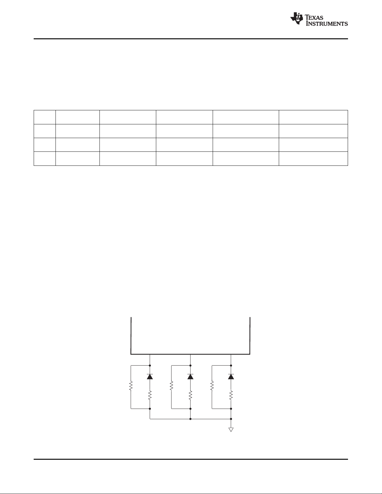
Note: Configuration pin option. See Section 2.7 for Jumper Definitions.
The definitions below define the functionality of each pin.
Type: I Input
Type: O Output
Type: I/O Input/Output
Type: OD Open Drain
Type: PD, PU Internal Pulldown/Pullup
Type: S Configuration Pin (All configuration pins have weak internal pullups or pulldowns. If
SLLS931–AUGUST 2009
a different default value is needed, then use an external 2.2kΩ resistor. See
Section 2.7 for details.)
2.1 Serial Management Interface
PIN
NAME NO.
MDC 32 I maximum MDC rate is 25 MHz; there is no minimum MDC rate. MDC is not required to be synchronous to the
MDIO 33 I/O
TYPE DESCRIPTION
MANAGEMENT DATA CLOCK: Clock signal for the management data input/output (MDIO) interface. The
MII_TX_CLK or the MII_RX_CLK.
MANAGEMENT DATA I/O: Bidirectional command / data signal synchronized to MDC. Either the local
controller or the TLK100 may drive the MDIO signal. This pin requires a pull-up resistor with value 1.5 kΩ.
Copyright © 2009, Texas Instruments Incorporated Pin Descriptions 5
Submit Documentation Feedback
Product Folder Link(s): TLK100

TLK100
SLLS931–AUGUST 2009
www.ti.com
2.2 MAC Data Interface
PIN
NAME NO.
MII_TX_CLK 19 O, PD
MII_TX_EN 18 I, PD MII_TX_CLK . It indicates the presence of valid data inputs on MII_TXD[3:0]. It is an
MII_TXD_0 13
MII_TXD_1 14 MII TRANSMIT DATA: The transmit data nibble received from the MAC that is
MII_TXD_2 15 synchronous to the rising edge of the MII_TX_CLK.
MII_TXD_3 16
MII_RX_CLK 23 O
MII_RX_DV 30 S, O, PD
MII_RX_ERR/MDIX_EN 31 S, O, PU
MII_RXD_0/PHYAD1 25
MII_RXD_1/PHYAD2 26
MII_RXD_2/PHYAD3 27
MII_RXD_3/PHYAD4 28
MII_CRS/LED_CFG 22 S, O, PU MII CARRIER SENSE: This pin is asserted high when the receive medium is non-idle.
MII_COL/PHYAD0 24 S, O, PU 10BASE-T/100BASE-TX half-duplex modes, this pin is asserted HIGH only when both
TYPE DESCRIPTION
MII TRANSMIT CLOCK: : MII Transmit Clock provides 25MHz or 2.5MHz reference
clock depending on the speed.
MII TRANSMIT ENABLE: MII_TX_EN is presented on the rising edge of the
active high signal.
IS, I, PD
MII RECEIVE CLOCK: MII receive clock provides a 25MHz or 2.5MHz reference clock,
depending on the speed, that is derived from the received data stream.
MII RECEIVE DATA VALID: This pin indicates valid data is present on the
corresponding MII_RXD[3:0].
MII RECEIVE ERROR: This pin indicates that an error symbol has been detected within
a received packet.
MII RECEIVE DATA: Symbols received on the cable are decoded and presented on
S, O, PD these pins synchronous to MII_RX_CLK. They contain valid data when MII_RX_DV is
asserted.
MII COLLISION DETECT: In Full Duplex Mode this pin is always low. In
the transmit and receive media are non-idle.
2.3 Clock Interface
PIN
NAME NO.
XI 39 I oscillator input. The TLK100 supports either an external crystal resonator connected across pins XI and
XO 37 O
CLK25OUT 12 O allows other devices to use the reference clock from the TLK100 without requiring additional clock
TYPE DESCRIPTION
CRYSTAL/OSCILLATOR INPUT: Reference clock. 25MHz ±50 ppm tolerance crystal reference or
XO, or an external CMOS-level oscillator source connected to pin XI only.
CRYSTAL OUTPUT: Reference Clock output. XO pin is used for crystal only. This pin should be left
floating when an oscillator input is connected to XI.
25 MHz CLOCK OUTPUT: In MII mode, this pin provides a 25 MHz clock output to the system. This
sources.
2.4 LED Interface
(See Table 3-3 for LED Mode Selection)
PIN
NAME NO.
LED_LINK/AN_0 36 S, O, PU Mode 2 and Mode 3, this pin indicates transmit and receive activity in addition to the status of the
LED_SPEED/AN_1 35 S, O, PU
LED_ACT/AN_EN 34 S, O, PU present on either Transmit or Receive channel. In Mode 3, this LED output may be programmed to
TYPE DESCRIPTION
This pin indicates the status of the link in Mode 1. When the link is good the LED will be ON. In
Link. The LED is ON when Link is good. It will blink when the transmitter or receiver is active.
This pin indicates the speed of the link. It is ON when the link speed is 100 Mb/s and OFF when it
is 10 Mb/s.
In mode 1 this pin indicates if there is any activity on the link. It is ON (pulse) when activity is
indicate Full-duplex status.
6 Pin Descriptions Copyright © 2009, Texas Instruments Incorporated
Submit Documentation Feedback
Product Folder Link(s): TLK100
TLK100
www.ti.com
SLLS931–AUGUST 2009
2.5 JTAG Interface
PIN
NAME NO.
JTAG_TCK 44 I, PU This pin is the test clock.This pin has a weak internal pullup.
JTAG_TDI 45 I, PU This pin is the test data input.This pin has a weak internal pullup.
JTAG_TDO 47 O This pin is the test data output.
JTAG_TMS 46 I, PU This pin selects the test mode. This pin has a weak internal pullup.
JTAG_TRST This pin is an active low asynchronous test reset. This pin has a weak internal pullup.
N
TYPE DESCRIPTION
48 I, PU
2.6 Reset and Power Down
PIN
NAME NO.
RESETN 43 I, PU TLK100. Asserting this pin low for at least 1 μs will force a reset process to occur. All jumper
PWRDNN/INT 42 I, OD, PU device is power down mode.
TYPE DESCRIPTION
This pin is an active Low reset input that initializes or re-initializes all the internal registers of the
options are reinitialized as well.
Register access is required for this pin to be configured either as power down or as an interrupt.
The default function of this pin is power down.
When this pin is configured for a power down function, an active low signal on this pin will put the
When this pin is configured as an interrupt pin then this pin is asserted low when an interrupt
condition occurs. The pin has an open-drain output with a weak internal pull-up. Some
applications may require an external pull-up resistor.
Copyright © 2009, Texas Instruments Incorporated Pin Descriptions 7
Submit Documentation Feedback
Product Folder Link(s): TLK100
TLK100
SLLS931–AUGUST 2009
2.7 Jumper Options
Jumper option is an elegant way to configure the TLK100 into specific modes of operation. Some of the
functional pins are used as jumper options. The logic states of these pins are sampled during reset and
are used to configure the device into specific modes of operation. Below table shows the pins used for the
jumper option and its description. The functional pin name is indicated in parentheses.
A 2.2 kΩ resistor should be used for pull-down or pull-up to change the default jumper option. If the default
option is required, then there is no need for external pull-up or pull down resistors. Since these pins may
have alternate functions after reset is deasserted, they should not be connected directly to VCC or GND.
PIN TYPE
NAME NO. DESCRIPTION
PHYAD0 (MII_COL) 24
PHYAD1 (MII_RXD_0) 25
PHYAD2 (MII_RXD_1) 26 S, O, PD
PHYAD3 (MII_RXD_2) 27
PHYAD4 (MII_RXD_3) 28
www.ti.com
The TLK100 provides five PHY address pins, the states of which are latched into an
internal register at system hardware reset. The TLK100 supports PHY Address jumpering
values 0 (<00000>) through 31 (<11111>). All PHYAD[4:0] pins have weak internal
pull-down resistors.
AN_EN: When high, this puts the part into advertised Auto-Negotiation mode with the
capability set by AN_0 and AN_1 pins. When low, this puts the part into Forced Mode with
the capability set by AN_0 and AN_1 pins.
AN_0 / AN_1: These input pins control the forced or advertised operating mode of the
TLK100 according to the following table. The value on these pins is set by connecting the
input pins to GND (0) or VCC (1) through 2.2 kΩ resistors. These pins should NEVER be
connected directly to GND or VCC.
The status of these pins are latched into the Basic Mode Control Register and the
Auto_Negotiation Advertisement Register during Hardware-Reset.
The default is 111 since these pins have internal pull-ups.
AN_EN (LED_ACT) 34
AN_1 (LED_SPEED) 35 S, O, PU
AN_0 (LED_LINK) 36
LED_CFG (MII_CRS) 22 S, O, PU the LED pins. Default is Mode 1. All modes are also configurable via register access. See
MDIX_EN (MII_RX_ERR) 31 S, O, PU
AN_EN AN_1 AN_0 Forced Mode
0 0 0 10BASE-T, Half-Duplex
0 0 1 10BASE-T, Full-Duplex
0 1 0 100BASE-TX, Half-Duplex
0 1 1 100BASE-TX, Full-Duplex
AN_EN AN_1 AN_0 Advertised Mode
1 0 0 10BASE-T, Half/Full-Duplex
1 0 1 10BASE-TX, Half/Full-Duplex
1 1 0
1 1 1
This jumpering option along with LEDCR register bit determines the mode of operation of
the table in the LED Interface Section.
This jumpering option sets the Auto-MDIX mode. By default it enables MDIX. An external
pull-down will disable Auto-MDIX mode.
10BASE-T, Half-Duplex
100BASE-TX, Half-Duplex
10BASE-T, Half/Full-Duplex
100BASE-TX, Half/Full-Duplex
8 Pin Descriptions Copyright © 2009, Texas Instruments Incorporated
Submit Documentation Feedback
Product Folder Link(s): TLK100

TLK100
www.ti.com
SLLS931–AUGUST 2009
2.8 10 Mb/s and 100 Mb/s PMD Interface
PIN
NAME NO.
TD–, TD+ 8, 9 I/O
RD–, RD+ 5, 6 I/O
TYPE DESCRIPTION
Differential common driver transmit output (PMD Output Pair). These differential outputs are automatically
configured to either 10BASE-T or 100BASE-TX signaling.
In Auto-MDIX mode of operation, this pair can be used as the Receive Input pair. These pins require 1.8V
or 3.3V bias for operation.
Differential receive input (PMD Input Pair). These differential inputs are automatically configured to accept
either 100BASE-TX or 10BASE-T signaling.
In Auto-MDIX mode of operation, this pair can be used as the Transmit Output pair. These pins require
1.8V or 3.3V bias for operation.
2.9 Power and Bias Connections
PIN
NAME NO.
RBIAS 3 I Bias Resistor Connection. Use a 4.99kΩ 1% resistor connected from RBIAS to GND.
V18_PFBOUT 40 O
VA11_PFBOUT 10 O
V18_PFBIN1 2
V18_PFBIN2 4
VA11_PFBIN1 1
VA11_PFBIN2 7
VDD11 20 O 1.1V Core Power Output. A capacitor of 1μF (Ceramic preferred) , should be placed close to the VDD11
VDD33_IO P I/O 3.3V Supply
VDD33_VA11 11 P This pin should be connected to 3.3V or 2.5V external supply, in single supply operation.
VDD33_V18 41 P In single supply operation, this pin should be connected to a 3.3V or 2.5V external supply. In multiple
VDD33_VD11 21 P This pin should be connected to 3.3V or 2.5V external supply, in single supply operation.
VSS 38 P Ground pin for Oscillator
GNDPAD 49 P Ground Pad
TYPE DESCRIPTION
1.8V Power Feedback Output. A 1μF capacitor (ceramic preferred), should be placed close to the
V18_PFBOUT.
In single supply operation, connect this pin should be connected to V18_PFBIN1 and V18_PFBIN2 (pin
2 and pin 4). See Figure 2-1 for proper placement pin.
In multiple supply operation, when supplying 1.8V from external supply, this pin should be connected
together with VDD33_V18 (pin 41), V18_PFBIN1 and V18_PFBIN2 (pin 2 and pin 4) to the 1.8V external
supply source. See Figure 2-2 for proper placement pin.
1.1V Analog Power Feedback Output. A 1 μF capacitor (Ceramic preferred), should be placed close to
the VA11_PFBOUT.
In single supply operation this pin should be connected to VA11_PFBIN1 and V11_PFBIN2 (pin 1 and
pin 7). See Figure 2-1 for proper placement pin.
In multiple supply operation, when supplying 1.1V from external supply, this pin should be connected
together with VDD33_VA11 (pin 11), V11_PFBIN1 and V11_PFBIN2 (pin 1 and pin 7) to 1.1V external
supply source. See Figure 2-3 for proper placement pin.
1.8V Power Feedback Input. These pins are fed with power from V18_PFBOUT (pin 40) in single supply
operation.
I
1.8V from external source in multiple supply operation. A small 1μF capacitor should be connected close
to each pin.
1.1V Analog Power Feedback Input. These pins are fed with power from: VA11_PFBOUT (pin 10) in
single supply operation.
I
1.1V from external source in multiple supply operation. A small capacitor of 0.1 μF should be connected
close to each pin.
17
29
External supply input to 1.1V analog regulator
In multiple supply operation this pin should be connected to external 1.1V supply source.
External supply input to 1.8V regulator
supply operation this pin should be connected to an external 1.8V supply source.
External supply input to 1.1V Core regulator
In multiple supply operation this pin should be connected to external 1.1V supply source.
Copyright © 2009, Texas Instruments Incorporated Pin Descriptions 9
Submit Documentation Feedback
Product Folder Link(s): TLK100
Vdd
Vdd
1 :1
1 :1
T1
RJ 45
3.3V
Supply
TLK100
11
VDD33_VA11
10
VA11_PFBOUT
1
VA11_PFBIN1
7
VA11_PFBIN2
21
VDD33_VD11
20
VDD11
.
17
VDD33_IO
29
VDD33_IO
5
RD–
RD–
6
RD+
RD+
49.9W
1.0 Fm
*
8
TD–
TD–
9
TD+
TD+
*
41
VDD33_V18
40
V18_PFBOUT
2
V18_PFBIN1
4
V18_PFBIN2
49.9W
49.9W
49.9W
0.1 Fm
0.1 Fm
0.1 Fm
0.1 Fm
0.1 Fm
0.1 Fm
0.1 Fm
3.3V
Supply
3.3V
Supply
0.1 Fm
1.0 Fm
1.0 Fm
TLK100
SLLS931–AUGUST 2009
2.10 Power Supply Configuration
The TLK100 provides best-in-class flexibility of power supplies.
• Single supply operation – If a single 3.3V power supply is desired, the TLK100 will sense the presence
of the supply and configure the internal voltage regulators to provide all necessary supply voltages. To
operate in this mode, connect the TLK100 supply pins according to the following scheme:
www.ti.com
Figure 2-1. Power Scheme for Single Supply Operation
• Multiple Supply operation – When additional 1.8V and/or 1.1V external power rails are available, the
TLK100 can be configured in various ways as given in Table 2-1. This gives the highest flexibility for
the user and enables significant reduction in power consumption. When using multiple external
supplies, the internal regulators must be disabled by appropriate device connections.
– When an external 1.8V rail is available – Connect the external 1.8V to all following TLK100 pins to
enable proper operation: V18_PFBOUT (pin 40), V18_PFBIN1 (pin 2), V18_PFBIN2 (pin 4) and
VDD33_V18 (pin 41). In addition, connect the 1.8V rail to the transformer center tap to further
reduce the transmission power, as shown in Figure 2-2:
10 Pin Descriptions Copyright © 2009, Texas Instruments Incorporated
Submit Documentation Feedback
Product Folder Link(s): TLK100
Pin 5
(RD–)
RD–
Pin 6
(RD+)
RD+
Vdd
1.8 V
Supply
Pin 8
(TD–)
TD–
Pin 9
(TD+)
TD+
Vdd
1:1
1:1
T1
RJ45
Pin 41
(VDD33_V18)
Pin 40
(V18_PFBOUT)
Pin 2
(V18_PFBIN)
Pin 4
(V18_PFBIN2)
1.8 V
Supply
TLK100
499 W
499 W
499 W
499 W
0.1 Fm
0.1 Fm
0.1 F*m
0.1 F*m
1.1 V
Supply
TLK100
Pin11
(VDD33_VA11)
Pin10
(VA11_PFBOUT)
Pin1
(VA11_PFBIN1)
Pin7
(VA11_PFBIN2)
Pin21
(VDD33_VA11)
Pin20
(VDD11)
TLK100
www.ti.com
SLLS931–AUGUST 2009
Figure 2-2. Power Scheme for Operation With External 1.8V Supply
– External 1.1V rail – When external 1.1V rail is available – Connect the external 1.1V to the following
pins: VA11_PFBOUT (pin 10), VDD11 (pin 20), VA11_PFBIN1 (pin 1), VA11_PFBIN2 (pin 7),
VDD33_VA11 (pin 11) and VDD33_VD11 (pin 21) as shown in Figure 2-3:
• Lowest-power operation – When 1.1V and 1.8V supplies are already available in addition to 3.3V,
designers can take advantage of the lowest-power configuration of the TLK100. By supplying external
1.8 and 1.1V as explained above, all the internal regulators are powered down and the device is fully
driven by the external supplies giving the lowest power operation.
Copyright © 2009, Texas Instruments Incorporated Pin Descriptions 11
Figure 2-3. Power Scheme for Operation With External 1.1V Supply
Submit Documentation Feedback
Product Folder Link(s): TLK100

TLK100
SLLS931–AUGUST 2009
Other power supply options – Because the TLK100 incorporates independent voltage regulators,
designers may take advantage of several optional configurations, depending on available power supplies.
See Table 2-1 for these options.
Table 2-1. Power Supply Options
MAC I/F Transformer CT
Mode
Single Supply 3.3V from 3.3V from 3.3V from 3.3V from
Operation external supply external supply external supply external supply
Lowest Power 3.3V from 1.8V from 1.8V from 1.1V from
Consumption external supply external supply external supply external supply
(3.3V) (3.3V or 1.8V)
Voltage Source Voltage Source Voltage Source Voltage Source
3.3V from 3.3V from 3.3V from 2.5V from
external supply external supply external supply external supply
3.3V from 3.3V from 3.3V from 1.1V from
external supply external supply external supply external supply
3.3V from 3.3V from 2.5V from 3.3V from
external supply external supply external supply external supply
3.3V from 3.3V from 2.5V from 2.5V from
external supply external supply external supply external supply
3.3V from 3.3V from 2.5V from 1.1V from
external supply external supply external supply external supply
3.3V from 1.8V from 1.8V from 3.3V from
external supply external supply external supply external supply
3.3V from 1.8V from 1.8V from 2.5V from
external supply external supply external supply external supply
Regulator Regulators
(ON/OFF) (ON/OFF)
ON ON
ON ON
ON OFF
ON ON
ON ON
ON OFF
OFF ON
OFF ON
OFF OFF
(1.8V) (1.1V)
www.ti.com
12 Pin Descriptions Copyright © 2009, Texas Instruments Incorporated
Submit Documentation Feedback
Product Folder Link(s): TLK100

TLK100
www.ti.com
3 Configuration
This section includes information on the various configuration options available with the TLK100. The
configuration options described below include:
• Auto-Negotiation
• Auto-MDIX
• PHY Address
• LED Interface
• Loopback Functionality
• BIST
• Cable Diagnostics
3.1 Auto-Negotiation
The TLK100 device can auto-negotiate to operate in 10BASE-T or 100BASE-TX. If Auto-Negotiation is
enabled, then the TLK100 device negotiates with the link partner to determine the speed and duplex with
which to operate. If the link partner is unable to Auto-Negotiate, the TLK100 device would go into the
parallel detect mode to determine the speed of the link partner. Under parallel detect mode, the duplex
mode is fixed at half-duplex.
The TLK100 supports four different Ethernet protocols (10 Mb/s Half Duplex, 10 Mb/s Full Duplex, 100
Mb/s Half Duplex, and 100 Mb/s Full Duplex), so the inclusion of Auto-Negotiation ensures that the
highest performance protocol will be selected based on the advertised ability of the Link Partner. The
Auto-Negotiation function within the TLK100 can be controlled either by internal register access or by the
use of the AN_EN, AN_1 and AN_0 pins.
SLLS931–AUGUST 2009
The state of AN_EN, AN_0 and AN_1 pins determines whether the TLK100 is forced into a specific mode
or Auto-Negotiation will advertise a specific ability (or set of abilities) as given in Table 2-1. These pins
allow configuration options to be selected without requiring internal register access. The state of AN_EN,
AN_0 and AN_1, upon power-up/reset, determines the state of bits [8:5] of the ANAR register (0x04h).
Table 3-1. Auto-Negotiation Modes
AN_EN AN_1 AN_0 Forced Mode
0 0 0 10BASE-T, Half-Duplex
0 0 1 10BASE-T, Full-Duplex
0 1 0 100BASE-TX, Half-Duplex
0 1 1 100BASE-TX, Full-Duplex
AN_EN AN_1 AN_0 Advertised Mode
1 0 0 10BASE-T, Half/Full-Duplex
1 0 1 10BASE-TX, Half/Full-Duplex
1 1 0 10BASE-T, Half Duplex
1 1 1 10BASE-T, Half/Full-Duplex
100BASE-TX, Half Duplex
100BASE-TX, Half/Full-Duplex
Copyright © 2009, Texas Instruments Incorporated Configuration 13
Submit Documentation Feedback
Product Folder Link(s): TLK100

TLK100
SLLS931–AUGUST 2009
The Auto-Negotiation function can also be controlled by internal register access using registers as defined
by the IEEE 802.3u specification. For further detail regarding Auto-Negotiation, see Clause 28 of the IEEE
802.3u specification.
3.2 Auto-MDIX
The TLK100 device automatically determines whether or not it needs to cross over between pairs so that
an external crossover cable is not required. If the TLK100 device interoperates with a device that
implements MDI/MDIX crossover, a random algorithm as described in IEEE 802.3 determines which
device performs the crossover.
Auto-MDIX is enabled by default and can be configured via jumper or via PHYCR (0x10h) register, bits
[6:5].
The crossover can be manually forced through bit 5 of PHYCR (0x10h) register. Neither Auto-Negotiation
nor Auto-MDIX is required to be enabled in forcing crossover of the MDI pairs.
Auto-MDIX can be used in the forced 100BT mode but not in the forced MDIX mode. As in modern
networks all the nodes are 100BT, having the Auto-MDIX working in the forced 100BT mode will resolve
the link faster without the need for the long Auto-Negotiation.
www.ti.com
14 Configuration Copyright © 2009, Texas Instruments Incorporated
Submit Documentation Feedback
Product Folder Link(s): TLK100
MII_COL
MII_RXD_0
MII_RXD_1
MII_RXD_2
MII_RXD_3
2.2kW
VCC
PHYAD4=0 PHYAD3=0 PHYAD2=0 PHYAD1=1 PHYAD0=1
B0314-01
TLK100
www.ti.com
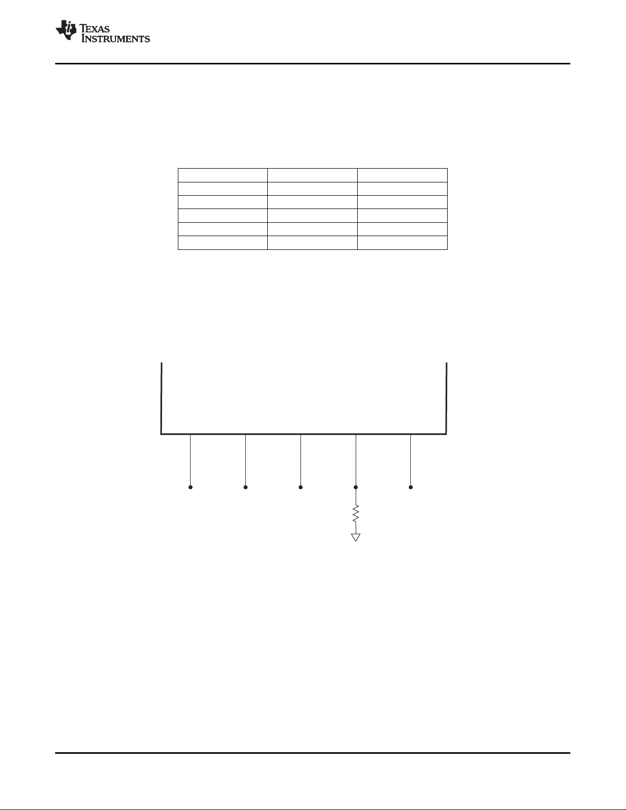
3.3 PHY Address
The 5 PHY address inputs pins are shared with the MII_RXD[3:0] pins and COL pin as shown in
Table 3-2.
Each TLK100 or port sharing an MDIO bus in a system must have a unique physical address. With 5
address input pins, the TLK100 can support PHY Address values 0 (<00000>) through 31 (<11111>). The
address-pin states are latched into an internal register at device power-up and hardware reset. Because
all the PHYAD[4:0] pins have weak internal pull-down resistors, the default setting for the PHY address is
00000 (0x00h).
See Figure 3-1 for an example of a PHYAD connection to external components. In this example, the
PHYAD configuration results in address 00010 (0x02h).
SLLS931–AUGUST 2009
Table 3-2. PHY Address Mapping
PIN # PHYAD FUNCTION RXD FUNCTION
24 PHYAD0 MII_COL
25 PHYAD1 MII_RXD_0
26 PHYAD2 MII_RXD_1
27 PHYAD3 MII_RXD_2
28 PHYAD4 MII_RXD_3
Figure 3-1. PHYAD Configuration Example
Copyright © 2009, Texas Instruments Incorporated Configuration 15
Submit Documentation Feedback
Product Folder Link(s): TLK100
LED_LINK
LED_SPEED
LED_ACT/COL
110 W 110 W110 W
2.2kW 2.2kW2.2kW
VCC
AN_EN=1 AN1=1 AN0=1
B0315-01
TLK100
SLLS931–AUGUST 2009
3.4 LED Interface
The TLK100 supports three configurable Light Emitting Diode (LED) pins. The device supports three LED
configurations: Link, Speed, and Activity. Functions are multiplexed among the LEDs into three modes.
The LEDs can be controlled by configuration pin and/or internal register bits. Bits 6:5 of the LED Direct
Control register (LEDCR) selects the LED mode as described in Table 3-3.
Table 3-3. LED Mode Select
Mode LED_LINK LED_SPEED LED_ACT
1 don't care 1
2 0 0
3 1 0
LED_CFG[1] LED_CFG[0]
(bit 6) (bit 5) or (pin 22)
ON for Good Link ON in 100 Mb/s ON Pulse for Activity
OFF for No Link OFF in 10 Mb/s OFF for No Activity
ON for Good Link ON in 100 Mb/s None
BLINK for Activity OFF in 10 Mb/s
ON for Good Link ON in 100 Mb/s ON for Full Duplex
BLINK for Activity OFF in 10 Mb/s OFF for Half Duplex
The LED_LINK pin in Mode 1 indicates the link status of the port. It is OFF when no LINK is present. In
Mode 2 and Mode 3 it is ON to indicate Link is good and BLINK to indicate activity is present on either
transmit or receive channel. The blink rate is decided by the bits 9:8 of the LEDCR register (0x18). The
default blink rate is 5Hz.
The LED_SPEED pin indicates 10 or 100 Mb/s data rate of the port. This LED is ON when the device is
operating in 100 Mb/s operation. The functionality of this LED is independent of mode selected.
www.ti.com
The LED_ACT pin in Mode 1 indicates the presence of either transmit or receive activity. The LED is ON
(Pulse) for Activity and OFF for No Activity. The width of the pulse is determined by the bits 14:13 of the
LEDCR register (0x18). The default pulse width is 200ms. In mode 3 this pin indicates the Duplex status
of operation. The LED is ON for Full Duplex and OFF for Half Duplex.
Bits 2:0 of the LEDCR register defines the polarity of the signals on the LED pins.
Since the Auto-Negotiation (AN) configuration options share the LED output pins, the external components
required for configuration-pin programming and those for LED usage must be considered in order to avoid
contention.
See Figure 3-2 for an example of AN connections to external components. In this example, the AN
programming results in Auto-Negotiation with 10/100 Half/Full-Duplex advertised.
16 Configuration Copyright © 2009, Texas Instruments Incorporated
Figure 3-2. AN Pin Configuration and LED Loading Example
Submit Documentation Feedback
Product Folder Link(s): TLK100
MAC/
Switch
PCS
Signal
Process
PHY
AFE
DigitalLoopback
PHY Digital
ExternalLoopback
AnalogLoopbackPCSLoopback
XFMR
RJ45
1
2
3
4
5
6
7
8
M
I
I
MIILoopback
TLK100
www.ti.com
3.5 Loopback Functionality
The TLK100 provides several options for Loopback that test and verify various functional blocks within the
PHY. Enabling loopback mode allows in-circuit testing of the TLK100 digital and analog data path.
Generally, the TLK100 may be configured to one of the Near-end loopback modes or to the Far-end
(reverse) loopback.
3.5.1 Near-End Loopback
Near-end loopback provides the ability to loop the transmitted data back to the receiver via the digital or
analog circuitry. The point at which the signal is looped back is selected using loopback control bits with
several options being provided. Figure 3-3 shows the PHY near-end loopback functionality.
SLLS931–AUGUST 2009
Figure 3-3. Block Diagram, Near-End Loopback Mode
The Near-end Loopback mode is selected by setting the respective bit in the BIST Control Register
(BISCR), MII register address 0x16. Bits 3:0 of the BISCR register are used to set the loopback mode
according to the following:
• Bit [0]: MII Loopback
• Bit [1]: PCS Loopback (in 100BaseTX only)
• Bit [2]: Digital Loopback
• Bit [3]: Analog Loopback
While in Loopback mode the data is looped back and also transmitted onto the media. To ensure proper
operation in Analog Loopback mode 100Ω terminations should be attached to the RJ45 connector.
External Loopback can be performed while working in normal mode (Bits 3:0 of the BISCR register are
assert to 0 and on RJ45 connector pin 1 is shorted to pin 3 and pin 2 is shorted to pin 6).
To maintain the desired operating mode, Auto-Negotiation should be disabled before selecting Loopback
mode. This is not relevant for external-loopback mode.
Copyright © 2009, Texas Instruments Incorporated Configuration 17
Submit Documentation Feedback
Product Folder Link(s): TLK100
MAC/
Switch
PCS
Signal
Process
PHY
AFE
PHY Digital
XFMR
&
RJ45
CAT5 Cable
LinkPartner
M
I
I
ReverseLoopback
TLK100
SLLS931–AUGUST 2009
3.5.2 Far-End Loopback
Far-end (Reverse) loopback is a special test mode to allow testing the PHY from link partner side. In this
mode data that is received from the link partner pass through the PHY's receiver, looped back on the MII
and transmitted back to the link partner. Figure 3-4 shows Far-end loopback functionality.
The Reverse Loopback mode is selected by setting bit 4 in the BIST Control Register (BISCR), MII
register address 0x16.
While in Reverse Loopback mode the data is looped back and also transmitted onto the MAC Interface
and all data signals that come from the MAC are ignored.
www.ti.com
Figure 3-4. Block Diagram, Far-End Loopback Mode
3.6 BIST
The TLK100 incorporates an internal PRBS Built-in Self Test (BIST) circuit to accommodate in-circuit
testing or diagnostics. The BIST circuit can be utilized to test the integrity of the transmit and receive data
paths. The BIST testing can be performed using both internal loopback (digital or analog) or external loop
back using a cable fixture. The BIST simulates a real data transfer scenarios using real packets on the
lines. The BIST allows full control of the packets lengths and of the Inter Packet Gap (IPG)
The BIST is implemented with independent transmit and receive paths, with the transmit block generating
a continuous stream of a pseudo random sequence. The TLK100 generates a 23-bit pseudo random
sequence for doing the BIST test. The received data is compared to the generated pseudo-random data
by the BIST Linear Feedback Shift Register (LFSR) to determine the BIST pass/fail status. The number of
error bytes that the PRBS checker received is stored in the BISECR register (0x72h).The number of
transmitted bytes that the PRBS checker received is stored in the BISBCR register (0x71h). The status of
whether the PRBS checker is locked to the incoming receive bit stream, whether the PRBS is in sync or
not and whether the packet generator is busy or not can be found by reading the BISSR register (0x17h).
The PRBS test can be put in a continuous mode or single mode by using the bit 15 of the BISCR register
(0x16h). In the continuous mode, when one of the PRBS counter reaches the maximum value the counter
starts counting from zero again. In the single mode when the PRBS counter reaches its maximum value
the PRBS checker stops counting.
TLK100 allows the user to control the length of the PRBS packet. By programming the BISPLR register
(0x7Bh) register one can set the length of the PRBS packet. There is also an option to generate a single
packet transmission of two types 64 and 1518 bytes through register bit – bit13 of the BISCR register
(0x16h). The single generated packet is composed of a constant data.
18 Configuration Copyright © 2009, Texas Instruments Incorporated
Submit Documentation Feedback
Product Folder Link(s): TLK100

TLK100
www.ti.com
3.7 Cable Diagnostics
With the vast deployment of Ethernet devices, the need for reliable, comprehensive and user-friendly
cable diagnostic tool is more important than ever. The wide variety of cables, topologies, and connectors
deployed results with the need to non-intrusively identify and report cable faults. TI cable diagnostic unit
provides extensive information about cable integrity.
The TLK100 offers the following capabilities in its Cable Diagnostic tools kit:
1. Time Domain Reflectometry (TDR).
2. Active Link Cable Diagnostic (ALCD).
3. Digital Spectrum Analyzer (DSA)
3.7.1 TDR
The TLK100 uses Time Domain Reflectometry (TDR) to determine the quality of the cables, connectors,
and terminations in addition to estimation of the cable length. Some of the possible problems that can be
diagnosed include opens, shorts, cable impedance mismatch, bad connectors, termination mismatches,
and any other discontinuities on the cable.
The TLK100 device transmits a test pulse of known amplitude (1V) down each of the two pairs of an
attached cable. The transmitted signal continues down the cable and reflects from each cable
imperfection, fault, bad connector and the end of the cable itself. After the pulse transmission the TLK100
measures the return time and amplitude of all these reflected pulses. This technique enables measuring
the distance and magnitude (impedance) of non-terminated cables (open or short), discontinuities (bad
connectors), and improperly-terminated cables with an accuracy of ±1m.
SLLS931–AUGUST 2009
To do this, the TLK100 uses a RAM with up to 256 samples to record all the input sampled data (Equals
to max possible measured cable length of over 200m). The TLK100 also uses soft data averaging to
reduce noise and improve accuracy. The TLK100 is capable of recording up to five reflections within the
tester pair. In case more than 5 reflections were recorded the TLK100 will save the last 5 of them.
For all TDR measurements, the transformation between time of arrival and physical distance is done by
the external host using minor computations (such as multiplication/addition and lookup tables). The host
must know the expected propagation delay of the cable, which depends, among other things, on the cable
category (e.g. CAT5/CAT5e/CAT6).
Copyright © 2009, Texas Instruments Incorporated Configuration 19
Submit Documentation Feedback
Product Folder Link(s): TLK100

TLK100
SLLS931–AUGUST 2009
3.7.2 ALCD
The TLK100 also supports Active Link Cable Diagnostic (ALCD). The ALCD offers a passive method to
estimate the cable length during active link. It uses passive digital signal processing based on adapted
data thus enabling measurement of cable length with an active link partner.
The ALCD also uses pre-defined parameters according to the cable properties (e.g. CAT5/CAT5e/CAT6)
in order to achieve higher accuracy in the estimated cable length. The ALCD Cable length measurement
accuracy is +/-5m for the pair used in the Rx path (due to the passive nature of the test we measure only
the pair on the Rx path).
3.7.3 DSA
The TLK100 also offers a unique capability of Digital Spectrum Analyzer (DSA). The DSA enables a very
detailed analysis of the channel frequency response (Magnitude only). The DSA has the following
capabilities:
• Produce channel frequency response in resolution of 119.2Hz.
• Save up to 512 bins per DSA run.
• Full control in the analyzed frequency bins location and resolution.
• Programmable options for input data for the DSA:
– Use raw data taken directly from the channel
– Use adapted data that passed digital signal processing
• Use additional filtering for smoothing the total channel frequency response.
• Build in averaging for more accurate results
www.ti.com
NOTE: For an example of the DSA output please see appendix A
To reset the cable diagnostic registers, set bit 14 of RAMCR2 register (0x0D01) to '1'. Writing software
global reset 0x001F bit 15 does not reset the cable diagnostic registers.
20 Configuration Copyright © 2009, Texas Instruments Incorporated
Submit Documentation Feedback
Product Folder Link(s): TLK100

TLK100
www.ti.com
4 Reset and Power Down Operation
At power up it is recommended to have the external reset pin (RESETN) active (low). The RESETN pin
should be de-asserted 200μs after the power is ramped up to allow the internal circuits to settle and for
the internal regulators to be stabilized. If required during normal operation, the device can be reset by a
hardware or software reset.
4.1 Hardware Reset
A hardware reset is accomplished by applying a low pulse (TTL level), with a duration of at least 1μs, to
the RESETN. This will reset the device such that all registers will be reinitialized to default values and the
hardware configuration values will be re-latched into the device (similar to the power-up/reset operation).
4.2 Software Reset
A software reset is accomplished by setting the reset bit (bit 15) of the BMCR register (0x00h). This bit
only resets the IEEE defined standard registers in the address space 0x00h to 0x07h. The software global
reset is accomplished by setting bit 15 of register PDN (0x001F) to ‘1’. This bit resets IEEE defined
registers (0x00h to 0x07h) and all the extended registers except for the cable-diagnostic registers and
RAM registers. For resetting the cable diagnostics and RAM registers, bit 14 of register RAMCR2
(0x0D01) should be set to ‘1’. The time from the point when the reset bit is set to the point the when
software reset has concluded is approximately 1.3 μs.
The software global reset resets the device such that all registers are reset to default values and the
hardware configuration values are maintained. Software driver code must wait 3 μs following a software
reset before allowing further serial MII operations with the TLK100.
SLLS931–AUGUST 2009
4.3 Power Down/Interrupt
The Power Down and Interrupt functions are multiplexed on pin 42 of the device. By default, this pin
functions as a power down input and the interrupt function is disabled. This pin can be configured as an
interrupt output pin by setting bit 15 (INTN_OE) to ‘1’ and bit 12 (INTN_OEN) to ‘0’ of the MINTCR (0x14h)
register. Bit 13 of the same MINTCR register is used to set the polarity of the interrupt.
4.3.1 Power Down Control Mode
The PWRDNN/INT pin can be asserted low to put the device in a Power Down mode. An external control
signal can be used to drive the pin low, overcoming the weak internal pull-up resistor. Alternatively, the
device can be configured to initialize into a Power Down state by use of an external pulldown resistor on
the PWRDNN/INT pin.
4.3.2 Interrupt Mechanisms
The interrupt function is controlled via register access. All interrupt sources are disabled by default. The
MINTMR register provides independent interrupt enable bits for the different interrupts supported by
TLK100. The PWRDNN/INT pin is asynchronously asserted low when an interrupt condition occurs. The
source of the interrupt can be determined by reading the interrupt status register MINTSR (0x13h). One or
more bits in the MINTSR will be set, denoting all currently pending interrupts. Reading of the MINTSR
clears ALL pending interrupts.
Copyright © 2009, Texas Instruments Incorporated Reset and Power Down Operation 21
Submit Documentation Feedback
Product Folder Link(s): TLK100

TLK100
SLLS931–AUGUST 2009
4.4 Power Down Modes
TLK100 supports four types of power saving modes. The lowest power consumption is in the "Extreme
Low Power" mode (ELP). To enter into the ELP mode the PWRDNN/INT pin is pulled LOW.
To enable the power-down modes described below, set bit 11 of register BMCR (0x00h) to '1'. In all
power-down modes, the entire PHY is powered down except for the SMI interface; the PHY stays in that
condition as long as the value of bit 11 of register BMCR (0x00h) remains '1'. When this bit is cleared, the
PHY powers up and returns to the last state it was in before it was powered down.
In General Power Down mode, bits 9 and 8 of the PHYCR register (0x10h) should be set to "01".
Additionally, bit 4 of the PHYCR register (0x10h) should be set to '1' so as to power down the internal PLL.
The SMI would operate on the reference clock.
In Active sleep mode, or Energy-Detect mode, every 1.4 seconds a Normal Link Pulse (NLP) is sent to
wake up the link-partner. To enter into the active sleep mode, bits 9 and 8 of register PHYCR (0x10h) is
set to "10". Automatic powerup is done when the link partner is detected.
In passive sleep mode, all core blocks are powered down. Automatic power-up is done when the link
partner is detected. To enter into the passive sleep mode, bits 9 and 8 of register PHYCR (0x10h) is set to
"11".
www.ti.com
22 Reset and Power Down Operation Copyright© 2009, Texas Instruments Incorporated
Submit Documentation Feedback
Product Folder Link(s): TLK100
RD–
RD–
RD+ RD+
49.9 W
49.9 W
Vdd
Vdd
0.1 Fm
0.1 F*m
TD– TD–
TD+
TD+
49.9 W
49.9 W
Vdd
0.1 Fm
0.1 F*m
1:1
1:1
T1
RJ45
Placeresistorsandcapacitorsclosetothedevice.
Common-modechokes
mayberequired.
Note:CentertapisconnectedtoVdd
*Placecapacitorsclosetothe
transformercentertaps
Allvaluesaretypicalandare 1%±
S0339-01
TLK100
www.ti.com
5 Design Guidelines
5.1 TPI Network Circuit
Figure 5-1 shows the recommended circuit for a 10/100 Mb/s twisted pair interface. Below is a partial list
of recommended transformers. It is important that the user realize that variations with PCB and
component characteristics require that the application be tested to verify that the circuit meets the
requirements of the intended application.
• Pulse H1102
• Pulse HX1188
SLLS931–AUGUST 2009
Figure 5-1. 10/100 Mb/s Twisted Pair Interface
5.2 Clock In (XI) Requirements
The TLK100 supports an external CMOS-level oscillator source or an internal oscillator with an external
crystal.
5.2.1 Oscillator
If an external clock source is used, XI should be tied to the clock source and XO should be left floating.
The amplitude of the oscillator should be a nominal voltage of 1.8V.
Copyright © 2009, Texas Instruments Incorporated Design Guidelines 23
Submit Documentation Feedback
Product Folder Link(s): TLK100

S0340-01
XI XO
R
1
C
L2
C
L1
TLK100
SLLS931–AUGUST 2009
5.2.2 Crystal
The use of a 25MHz, parallel, 20pF-load crystal resonator is recommended if a crystal source is desired.
Figure 5-2 shows a typical connection for a crystal resonator circuit. The load capacitor values will vary
with the crystal vendors; check with the vendor for the recommended loads.
The oscillator circuit is designed to drive a parallel resonance AT-cut crystal with a minimum drive level of
100μW and a maximum of 500μW. If a crystal is specified for a lower drive level, a current limiting resistor
should be placed in series between XO and the crystal.
As a starting point for evaluating an oscillator circuit, if the requirements for the crystal are not known, set
the values for CL1and CL2at 33pF, and R1should be set at 0Ω.
Specification for 25MHz crystal are listed in Table 5-2.
www.ti.com
Figure 5-2. Crystal Oscillator Circuit
Table 5-1. 25 MHz Oscillator Specification
PARAMETER TEST CONDITIONS MIN TYP MAX UNIT
Frequency 25 MHz
Frequency Tolerance Operational Temperature ±50 ppm
Frequency Stability 1 year aging ±50 ppm
Rise / Fall Time 10%–90% 8 nsec
Jitter (Short term) Cycle-to-cycle 50 psec
Jitter (Long term) Accumulative over 10 ms 1 nsec
Symmetry Duty Cycle 40% 60%
Load Capacitance 15 30 pF
Table 5-2. 25 MHz Crystal Specification
PARAMETER TEST CONDITIONS MIN TYP MAX UNIT
Frequency 25 MHz
Frequency Tolerance Operational Temperature ±50 ppm
At 25°C ±50 ppm
Frequency Stability 1 year aging ±5 ppm
Load Capacitance 10 40 pF
24 Design Guidelines Copyright © 2009, Texas Instruments Incorporated
Submit Documentation Feedback
Product Folder Link(s): TLK100

M0117-01
TLK100
www.ti.com
5.3 Thermal Vias Recommendation
The following thermal via guidelines apply to GNDPAD, pin 49:
1. Thermal via size = 0.2 mm
2. Recommend 4 vias
3. Vias have a center to center separation of 2 mm.
Adherence to this guideline is required to achieve the intended operating temperature range of the device.
Figure 5-3 illustrates an example layout.
SLLS931–AUGUST 2009
Figure 5-3. Example Layout
Copyright © 2009, Texas Instruments Incorporated Design Guidelines 25
Submit Documentation Feedback
Product Folder Link(s): TLK100

TLK100
SLLS931–AUGUST 2009
6 Register Block
Table 6-1. Register Map
OFFSET HEX ACCESS TAG DESCRIPTION
00h RW BMCR Basic Mode Control Register
01h RO BMSR Basic Mode Status Register
02h RO PHYIDR1 PHY Identifier Register #1
03h RO PHYIDR2 PHY Identifier Register #2
04h RW ANAR Auto-Negotiation Advertisement Register
05h RO ANLPAR Auto-Negotiation Link Partner Ability Register
06h RO ANER Auto-Negotiation Expansion Register
07h RW ANNPTR Auto-Negotiation Next Page TX
08h RO ANLNPTR Auto-Negotiation Link Partner Ability Next Page Register
09h–0Ch RW RESERVED RESERVED
0Dh RW REGCR Register control register
0Eh RW ADDAR Address or Data register
0Fh RW RESERVED RESERVED
EXTENDED REGISTERS
10h RW PHYCR PHY Control Register
11h RO PHYSR PHY Status Register
12h RW MINTMR MII Interrupt Mask Register
13h RO MINTSR MII Interrupt Status Register
14h RW MINTCR MII Interrupt Control Register
15h RO RECR Receive Error Counter Register
16h RW BISCR BIST Control Register
17h RO BISSR BIST Status Register
18h RW LEDCR LED Direct Control Register
19h RW RESERVED RESERVED
1Ah RW CDCR Cable Diagnostic Control Register
1Bh RW CDSR Cable Diagnostic Status Register
1Ch RO CDRR Cable Diagnostic Results Register
1Dh-1Eh RW RESERVED RESERVED
1Fh RW PDR Power Down Register
42h RO FCSCR False Carrier Sense Counter Register
70h RW RXCCR RX Channel Control Register
71h RO BISBCR BIST Byte Count Register
72h RO BISECR BIST Error Count Register
7Bh RW BISPLR BIST Packet Length Register
7Ch RW BISIPGR BIST Inter Packet Gap Register
80h RW TDRSMR TDR State Machine Enable Register
90h RW TDRPAR TDR Pattern Amplitude Register
94h RW TDRMPR TDR Manual Pulse Register
0C00h–0C0Ch RW TDR Algorithm Registers
0C26h–0C2Ah RW ALCD/DSA Registers
0D00h, 0D01h, RAM registers
0D04h
0107h RW CD Pre Test Configuration 1 Register
010Fh RW CD Pre Test Configuration 2 Register
00AC RW LPF Bypass Register
RW
www.ti.com
26 Register Block Copyright © 2009, Texas Instruments Incorporated
Submit Documentation Feedback
Product Folder Link(s): TLK100

TLK100
www.ti.com
SLLS931–AUGUST 2009
Copyright © 2009, Texas Instruments Incorporated Register Block 27
Submit Documentation Feedback
Product Folder Link(s): TLK100

TLK100
SLLS931–AUGUST 2009
www.ti.com
Table 6-2. Register Table
Register Name Addr Tag Bit 15 Bit 14 Bit 13 Bit 12 Bit 11 Bit 10 Bit 9 Bit 8 Bit 7 Bit 6 Bit 5 Bit 4 Bit 3 Bit 2 Bit 1 Bit 0
Basic Mode Control 00h BMCR Reset Loopback Speed Auto-Neg Power Isolate Restart Duplex Collision Reserved Reserved Reserved Reserved Reserved Reserved Reserved
Register Selection Enable Down Auto-Neg Mode Test
Basic Mode Status 01h BMSR 100Base 100Base 100Base 10Base-T 10Base-T Reserved Reserved Reserved Reserved MF Auto-Neg Remote Auto-Neg Link Status Jabber Extended
Register -T4 -TX FDX -TX HDX FDX HDX Preamble Complete Fault Ability Detect Capability
PHY Identifier 02h PHYIDR 1 OUI MSB OUI MSB OUI MSB OUI MSB OUI MSB OUI MSB OUI MSB OUI MSB OUI MSB OUI MSB OUI MSB OUI MSB OUI MSB OUI MSB OUI MSB OUI MSB
Register 1
PHY Identifier 03h PHYIDR 2 OUI LSB OUI LSB OUI LSB OUI LSB OUI LSB OUI LSB VNDR_ VNDR_ VNDR_ VNDR_ VNDR_ VNDR_ MDL_ REV MDL_ REV MDL_ REV MDL_ REV
Register 2 MDL MDL MDL MDL MDL MDL
Auto-Negotiation 04h ANAR Next Page Reserved Remote Reserved ASM_DI R PAUSE T4 TX_FD TX 10_FD 10 Protocol Protocol Protocol Protocol Protocol
Advertisement Ind Fault Selection Selection Selection Selection Selection
Register
Auto-Negotiation Link 05h ANLPAR Next Page ACK Remote Reserved ASM_DI R PAUSE T4 TX_FD TX 10_FD 10 Protocol Protocol Protocol Protocol Protocol
Partner Ability Ind Fault Selection Selection Selection Selection Selection
Register (Base Page)
Auto-Negotiation 06h ANER Reserved Reserved Reserved Reserved Reserved Reserved Reserved Reserved Reserved Reserved Reserved PDF LP_NP_ NP_ ABLE PAGE_ RX LP_AN_AB
Expansion Register ABLE LE
Auto-Negotiation Next 07h ANNPTR Next Page Reserved Message ACK2 TOG_TX CODE CODE CODE CODE CODE CODE CODE CODE CODE CODE CODE
Page TX Register Ind Page
Auto-Negotiate Link 08h ANLNPTR Next Page Reserved Message ACK2 TOG_TX CODE CODE CODE CODE CODE CODE CODE CODE CODE CODE CODE
Partner Ability Page Ind Page
Register
RESERVED 09-0Ch Reserved Reserved Reserved Reserved Reserved Reserved Reserved Reserved Reserved Reserved Reserved Reserved Reserved Reserved Reserved Reserved Reserved
Register Control 0Dh REGCR Function Function Reserved Reserved Reserved Reserved Reserved Reserved Reserved Reserved Reserved DEVICE DEVICE DEVICE DEVICE DEVICE
Register ADDRESS ADDRESS ADDRESS ADDRESS ADDRESS
Address or Data 0Eh ADDAR Addr/ Data Addr/ Data Addr /Data Addr /Data Addr/ Data Addr/ Data Addr /Data Addr /Data Addr/ Data Addr/ Data Addr /Data Addr /Data Addr/ Data Addr/ Data Addr /Data Addr /Data
Register
RESERVED 0Fh Reserved Reserved Reserved Reserved Reserved Reserved Reserved Reserved Reserved Reserved Reserved Reserved Reserved Reserved Reserved Reserved Reserved
EXTENDED REGISTERS
PHY Control Register 10h PHYCR TX FIFO TX FIFO Reserved Reserved Reserved Force Link Power Power Reserved Auto MDI-X Manual Disable Reserved Reserved Reserved Disable
PHY Status Register 11h PHYSR Reserved Speed Duplex Page AutoNego Link Status Reserved MDI Cross Reserved Sleep Reserved Reserved Reserved Reserved Polarity Jabber
MII Interrupt Mask 12h MINTMR Auto Nego Speed Duplex Page Auto Nego Link Status Reserved Reserved FIFO Over MDI cross Reserved Sleep Reserved Reserved Polarity Jabber
Register error Change Mode Received Complete Change Under flow over Mode Change Interrupt
MII Interrupt Status 13h MINTSR Auto Nego Speed Duplex Page Auto Nego Link Status Reserved Reserved FIFO Over MDI Reserved Sleep Reserved Reserved Polarity Jabber
Register Error Changed Mode Received Complete Changed Underflow Crossover Mode Changed
MII Interrupt Control 14h MINTCR Interrupt Reserved Interrupt Interrupt Reserved Reserved Reserved Reserved Reserved Reserved Reserved Reserved Reserved Reserved Reserved Reserved
Register Pin Enable Polarity Pin Enable
Receive Error 15h RECR RXCERNT RXCERNT RXCERNT RXCERNT RXCERNT RXCERNT RXCERNT RXCERNT RXERCNT RXERCNT RXERCNT RXERCNT RXERCNT RXERCNT RXERCNT RXERCNT
Counter Register
BIST Control Register 16h BISCR PRBS Generate 64 bit mode Packet Reserved Reserved Reserved Reserved Reserved Reserved Reserved Loopback Loop back Loop back Loop back Loop back
Depth Depth Good Down Mode Down Mode Enable MDI-X PLL Jabber
Received Complete over Mode
Enable Enable Change Enable Enable Enable Enable change Change Enable Enable
Count PRBS Generation Mode Mode Mode Mode Mode
Mode Packets Enable
Enable Enable Enable
Changed Changed Changed
Suppress
Enable
28 Register Block Copyright © 2009, Texas Instruments Incorporated
Submit Documentation Feedback
Product Folder Link(s): TLK100

TLK100
www.ti.com
SLLS931–AUGUST 2009
Table 6-2. Register Table (continued)
Register Name Addr Tag Bit 15 Bit 14 Bit 13 Bit 12 Bit 11 Bit 10 Bit 9 Bit 8 Bit 7 Bit 6 Bit 5 Bit 4 Bit 3 Bit 2 Bit 1 Bit 0
BIST Status Register 17h BISSR Reserved Reserved Reserved Reserved PRBS PRBS Sync PRBS Core Power Reserved Reserved Reserved Reserved Reserved Reserved Reserved Reserved
BIST Byte Count 71h BISBCR PRBS PRBS PRBS PRBS PRBS PRBS PRBS PRBS PRBS PRBS PRBS PRBS PRBS PRBS PRBS PRBS
Register Count Count Count Count Count Count Count Count Count Count Count Count Count Count Count Count
BIST Error Count 72h BISECR Reserved Reserved Reserved Reserved Reserved Reserved Reserved Reserved PRBS Error PRBS Error PRBS Error PRBS Error PRBS Error PRBS Error PRBS Error PRBS Error
Register Count Count Count Count Count Count Count Count
BIST Packet Length 7Bh BISPLR PRBS PRBS PRBS PRBS PRBS PRBS PRBS PRBS PRBS PRBS PRBS PRBS PRBS PRBS PRBS PRBS
register Packet Packet Packet Packet Packet Packet Packet Packet Packet Packet Packet Packet Packet Packet Packet Packet
BIST Inter Packet 7Ch BISIPGR PRBS IPG PRBS IPG PRBS IPG PRBS IPG PRBS IPG PRBS IPG PRBS IPG PRBS IPG PRBS IPG PRBS IPG PRBS IPG PRBS IPG PRBS IPG PRBS IPG PRBS IPG PRBS IPG
Gap Register Length Length Length Length Length Length Length Length Length Length Length Length Length Length Length Length
LED Control Register 18h LEDCR LED Pulse Width Pulse Width Force Reserved Reserved Blink Rate Blink Rate Reserved LED Mode LED Mode Reserved Reserved LED ACT LED LED LINK
Power Down Register 1Fh PDR Software Reserved Reserved Reserved Reserved Reserved Reserved Reserved Reserved Reserved Reserved Reserved Reserved Reserved Reserved Reserved
False Carrier Sense 42h FCSCR Reserved Reserved Reserved Reserved Reserved Reserved Reserved Reserved Idle_error_c Idle_error_c Idle_error_c Idle_error_c Idle_error_c Idle_error_c Idle_error_c Idle_error_c
Counter Register ount ount ount ount ount ount ount ount
RX Channel Control 70h RXCCR Rese-rved Rese-rved Rese-rved Reserved Reserved Reserved Reserved Reserved Reserved Reserved Reserved Reserved Polarity Mdix Reserved Reserved
Register Inversion
Cable Diagnostic 1Ah CDCR Reserved Reserved ALCD/ DSA TDR test Reserved Cable Diag Cable Diag Cable Diag Reserved Reserved Reserved Reserved Reserved Reserved Reserved Channel
Register test start Start result result result Select
Cable Diagnostic 1Bh CDSR ALCD/ DSA TDR Fail TDR Done Reserved Reserved Reserved DSA Input DSA Input DSA Input DSA Input DSA ALCD/ DSA Reserved Reserved Reserved Reserved
Status Register Done Signal Signal Signal Signal Enalbe mode
Cable Diagnostic 1Ch CDRR Cable Diag Cable Diag Cable Diag Cable Diag Cable Diag Cable Diag Cable Diag Cable Diag Cable Diag Cable Diag Cable Diag Cable Diag Cable Diag Cable Diag Cable Diag Cable Diag
Results Register Results Results Results Results Results Results Results Results Results Results Results Results Results Results Results Results
TDR State Machine 80h TDRSMR Cmn_tdr_ Cmn_tdr Reserved Reserved Reserved Reserved Reserved Reserved Reserved Reserved Reserved Reserved Reserved Reserved Reserved Reserved
Enable sm_mode _tx_sm_
TDR Pattern 90h TDRPAR Rese- rved Rese- rved Rese- rved Rese- rved Rese- rved Rese- rved Rese- rved Rese- rved Rese- rved Rese- rved Rese- rved TDR TDR TDR TDR TDR
Amplitude Register pattern pattern pattern pattern pattern
TDR Manual Pulse 94h TDRMPR Rese-rved Rese-rved Rese-rved Reserved Reserved Reserved Reserved Reserved Reserved Reserved Reserved Reserved Reserved Reserved TDR_TX Reserved
Register _START
TDR Algorithm
Registers
ALCD/DSA Registers 0C26h – 0C2Ah
CD Pre test 0107h, 010Fh
Configuration
LPF Bypass Register 00ACh
0C00h – 0C0Ch
Length Length Length Length Length Length Length Length Length Length Length Length Length Length Length Length
Enable Interrupt Polarity SPEED Polarity
Global
Reset
mode
Cable Diagnostic algorithmrelated registers
Locked Loss Generator Mode
Select Select Select
busy Status
Polarity
Copyright © 2009, Texas Instruments Incorporated Register Block 29
Submit Documentation Feedback
Product Folder Link(s): TLK100

TLK100
SLLS931–AUGUST 2009
6.1 Register Definition
In the register definitions under the ‘Default’ heading, the following definitions hold true:
• RW = Read Write access
• SC = Register sets on event occurrence and Self-Clears when event ends
• RW/SC = Read Write Access/Self Clearing bit
• RO = Read Only access
• COR = Clear on Read
• RO/COR = Read Only, Clear on Read
• RO/P = Read Only, Permanently set to a default value
• LL = Latched Low and held until read, based upon the occurrence of the corresponding event
• LH = Latched High and held until read, based upon the occurrence of the corresponding event
www.ti.com
30 Register Block Copyright © 2009, Texas Instruments Incorporated
Submit Documentation Feedback
Product Folder Link(s): TLK100

TLK100
www.ti.com
6.1.1 Basic Mode Control Register (BMCR)
Table 6-3. Basic Mode Control Register (BMCR), address 0x0000
BIT BIT NAME DEFAULT DESCRIPTION
15 Reset 0, RW/SC PHY Software Reset:
1 = Initiate software Reset / Reset in Process.
0 = Normal operation.
Writing a 1 to this bit causes the PHY to be reset. When the reset operation is done, this bit
is cleared to 0 automatically. The configuration is relatched.
14 Loopback 0, RW Loopback:
1 = Loopback enabled.
0 = Normal operation.
When loopback mode is activated, the transmitter data presented on TXD is looped back to
RXD internally
13 Speed Selection Jumper, RW Speed Select:
When auto-negotiation is disabled writing to this bit allows the port speed to be selected.
1 = 100 Mb/s
0 = 10 Mb/s
12 Auto-Negotiation Jumper, RW Auto-Negotiation Enable:
Enable
11 Power Down 0, RW Power Down:
10 Isolate 0, RW Isolate:
9 Restart Auto- 0, RW/SC Restart Auto-Negotiation:
Negotiation
8 Duplex Mode Jumper, RW Duplex Mode:
7 Collision Test 0, RW Collision Test:
6:0 RESERVED 0, RO RESERVED: Write ignored, read as 0.
Configuration pin (jumper) controls initial value at reset.
1 = Auto-Negotiation Enabled – bits 8 and 13 of this register are ignored when this bit is
set.
0 = Auto-Negotiation Disabled – bits 8 and 13 determine the port speed and duplex
mode.
1 = Enables Power Down Modes - General Power Down Mode, Active Sleep Mode and
Passive Sleep Mode (see register 0x10)
0 = Normal operation.
1 = Isolates the Port from the MII with the exception of the serial management.
0 = Normal operation.
1 = Restart Auto-Negotiation. Re-initiates the Auto-Negotiation process. If
Auto-Negotiation is disabled (bit 12 = 0), this bit is ignored. This bit is self-clearing
and will return a value of 1 until Auto-Negotiation is initiated, whereupon it will
self-clear. Operation of the Auto-Negotiation process is not affected by the
management entity clearing this bit.
0 = Normal operation.
Re-initiates the Auto-Negotiation process. If Auto-Negotiation is disabled (bit 12 = 0), this bit
is ignored. This bit is self-clearing and will return a value of 1 until Auto-Negotiation is
initiated, whereupon it self-clears. Operation of the Auto-Negotiation process is not affected
by the management entity clearing this bit.
When auto-negotiation is disabled writing to this bit allows the port Duplex capability to be
selected.
1 = Full Duplex operation.
0 = Half Duplex operation.
1 = Collision test enabled.
0 = Normal operation
SLLS931–AUGUST 2009
Copyright © 2009, Texas Instruments Incorporated Register Block 31
Submit Documentation Feedback
Product Folder Link(s): TLK100

TLK100
SLLS931–AUGUST 2009
6.1.2 Basic Mode Status Register (BMSR)
Table 6-4. Basic Mode Status Register (BMSR), address 0x0001
BIT BIT NAME DEFAULT DESCRIPTION
15 100BASE-T4 0, RO/P 100BASE-T4 Capable:
This protocol is not available. Always 0 = Device does not perform 100BASE-T4 mode.
14 100BASE-TX 1, RO/P 100BASE-TX Full Duplex Capable:
Full Duplex
13 100BASE-TX 1, RO/P 100BASE-TX Half Duplex Capable:
Half Duplex
12 10BASE-T 1, RO/P 10BASE-T Full Duplex Capable:
Full Duplex
11 10BASE-T 1, RO/P 10BASE-T Half Duplex Capable:
Half Duplex
10: RESERVED 0, RO RESERVED: Write as 0, read as 0.
7
6 MF Preamble 1, RO/P Preamble suppression Capable:
Suppression
5 Auto- 0, RO Auto-Negotiation Complete:
Negotiation
Complete
4 Remote Fault 0, RO/LH Remote Fault:
3 Auto- 1, RO/P Auto Negotiation Ability:
Negotiation
Ability
2 Link Status 0, RO/LL Link Status:
1 Jabber Detect 0, RO/LH Jabber Detect: This bit only has meaning in 10 Mb/s mode.
0 Extended 1, RO/P Extended Capability:
Capability
1 = Device able to perform 100BASE-TX in full duplex mode.
0 = Device not able to perform 100BASE-TX in full duplex mode.
1 = Device able to perform 100BASE-TX in half duplex mode.
0 = Device not able to perform 100BASE-TX in half duplex mode.
1 = Device able to perform 10BASE-T in full duplex mode.
0 = Device not able to perform 10BASE-T in full duplex mode.
1 = Device able to perform 10BASE-T in half duplex mode.
0 = Device not able to perform 10BASE-T in half duplex mode.
1 = Device able to perform management transaction with preamble suppressed, 32-bits of preamble
needed only once after reset, invalid opcode or invalid turnaround.
0 = Device will not perform management transaction with preambles suppressed.
1 = Auto-Negotiation process complete.
0 = Auto-Negotiation process not complete (either still in process, disabled, or reset)
1 = Remote Fault condition detected (cleared on read or by reset). Fault criteria: Far End Fault
Indication or notification from Link Partner of Remote Fault.
0 = No remote fault condition detected.
1 = Device is able to perform Auto-Negotiation.
0 = Device is not able to perform Auto-Negotiation.
1 = Valid link established (for either 10 or 100 Mb/s operation).
0 = Link not established.
1 = Jabber condition detected.
0 = No Jabber. condition detected.
1 = Extended register capabilities.
0 = Basic register set capabilities only.
www.ti.com
The PHY Identifier Registers #1 and #2 together form a unique identifier for the TLK100. The Identifier
consists of a concatenation of the Organizationally Unique Identifier (OUI), the vendor's model number
and the model revision number. A PHY may return a value of zero in each of the 32 bits of the PHY
Identifier if desired. The PHY Identifier is intended to support network management. The IEEE-assigned
OUI for Texas Instruments is 080028h.
32 Register Block Copyright © 2009, Texas Instruments Incorporated
Submit Documentation Feedback
Product Folder Link(s): TLK100

TLK100
www.ti.com
SLLS931–AUGUST 2009
6.1.3 PHY Identifier Register #1 (PHYIDR1)
Table 6-5. PHY Identifier Register #1 (PHYIDR1), address 0x0002
BIT BIT NAME DEFAULT DESCRIPTION
15 OUI_MSB <0010 0000 0000 OUI Most Significant Bits: Bits 3 to 18 of the OUI (080028h) are stored in bits 15 to 0 of
0000>, this register. The most significant two bits of the OUI are ignored (the IEEE standard refers
RO/P to these as bits 1 and 2).
6.1.4 PHY Identifier Register #2 (PHYIDR2)
Table 6-6. PHY Identifier Register #2 (PHYIDR2), address 0x0003
BIT BIT NAME DEFAULT DESCRIPTION
15:10 OUI_LSB <101000>, OUI Least Significant Bits:
9:4 VNDR_MDL <100000>, Vendor Model Number:
3:0 MDL_REV <0001>, RO/P Model Revision Number:
RO/P
RO/P
Bits 19 to 24 of the OUI (080028h) are mapped from bits 15 to 10 of this register respectively.
The six bits of vendor model number are mapped from bits 9 to 4 (most significant bit to bit 9).
Four bits of the vendor model revision number are mapped from bits 3 to 0 (most significant bit to
bit 3). This field is incremented for all major device changes.
Copyright © 2009, Texas Instruments Incorporated Register Block 33
Submit Documentation Feedback
Product Folder Link(s): TLK100

TLK100
SLLS931–AUGUST 2009
6.1.5 Auto-Negotiation Advertisement Register (ANAR)
This register contains the advertised abilities of this device as they are transmitted to its link partner during
Auto- Negotiation.
Table 6-7. Auto Negotiation Advertisement Register (ANAR), address 0x0004
BIT BIT NAME DEFAULT DESCRIPTION
15 NP 0, RW Next Page Indication:
0 = Next Page Transfer not desired.
1 = Next Page Transfer desired.
14 RESERVED 0, RO/P RESERVED by IEEE: Writes ignored, Read as 0.
13 RF 0, RW Remote Fault:
1 = Advertises that this device has detected a Remote Fault.
0 = No Remote Fault detected.
12 RESERVED 0, RW RESERVED for Future IEEE use: Write as 0, Read as 0
11 ASM_DIR 0, RW Asymmetric PAUSE Support for Full Duplex Links:
1 = Asymmetric PAUSE implemented.
0 = Asymmetric PAUSE not implemented.
10 PAUSE 0, RW PAUSE Support for Full Duplex Links:
1 = MAC PAUSE implemented
0 = MAC PAUSE not implemented
9 T4 0, RO/P 100BASE-T4 Support:
1 = 100BASE-T4 is supported by the local device.
0 = 100BASE-T4 not supported.
8 TX_FD Jumper, RW 100BASE-TX Full Duplex Support:
1 = 100BASE-TX Full Duplex is supported by the local device.
0 = 100BASE-TX Full Duplex not supported.
7 TX Jumper, RW 100BASE-TX Support:
1 = 100BASE-TX is supported by the local device.
0 = 100BASE-TX not supported.
6 10_FD Jumper, RW 10BASE-T Full Duplex Support:
1 = 10BASE-T Full Duplex is supported by the local device.
0 = 10BASE-T Full Duplex not supported.
5 10 Jumper, RW 10BASE-T Support:
1 = 10BASE-T is supported by the local device.
0 = 10BASE-T not supported.
4:0 Selector <00001>, RW Protocol Selection Bits:
These bits contain the binary encoded protocol selector supported by this port. <00001> indicates that
this device supports IEEE 802.3u.
www.ti.com
34 Register Block Copyright © 2009, Texas Instruments Incorporated
Submit Documentation Feedback
Product Folder Link(s): TLK100

TLK100
www.ti.com
SLLS931–AUGUST 2009
6.1.6 Auto-Negotiation Link Partner Ability Register (ANLPAR) (BASE Page)
This register contains the advertised abilities of the Link Partner as received during Auto-Negotiation. The
content changes after the successful auto-negotiation if Next-pages are supported.
Table 6-8. Auto-Negotiation Link Partner Ability Register (ANLPAR) (BASE Page), address 0x0005
BIT BIT NAME DEFAULT DESCRIPTION
15 NP 0, RO Next Page Indication:
0 = Link Partner does not desire Next Page Transfer.
1 = Link Partner desires Next Page Transfer.
14 ACK 0, RO Acknowledge:
1 = Link Partner acknowledges reception of the ability data word.
0 = Not acknowledged. The Auto-Negotiation state machine will automatically control the this bit
based on the incoming FLP bursts.
13 RF 0, RO Remote Fault:
1 = Remote Fault indicated by Link Partner.
0 = No Remote Fault indicated by Link Partner.
12 RESERVED 0, RO RESERVED for Future IEEE use: Write as 0, read as 0.
11 ASM_DIR 0, RO ASYMMETRIC PAUSE:
1 = Asymmetric pause is supported by the Link Partner.
0 = Asymmetric pause is not supported by the Link Partner.
10 PAUSE 0, RO PAUSE:
1 = Pause function is supported by the Link Partner.
0 = Pause function is not supported by the Link Partner.
9 T4 0, RO 100BASE-T4 Support:
1 = 100BASE-T4 is supported by the Link Partner.
0 = 100BASE-T4 is not supported by the Link Partner.
8 TX_FD 0, RO 100BASE-TX Full Duplex Support:
1 = 100BASE-TX Full Duplex is supported by the Link Partner.
0 = 100BASE-TX Full Duplex is not supported by the Link Partner.
7 TX 0, RO 100BASE-TX Support:
1 = 100BASE-TX is supported by the Link Partner.
0 = 100BASE-TX is not supported by the Link Partner.
6 10_FD 0, RO 10BASE-T Full Duplex Support:
1 = 10BASE-T Full Duplex is supported by the Link Partner.
0 = 10BASE-T Full Duplex is not supported by the Link Partner.
5 10 0, RO 10BASE-T Support:
1 = 10BASE-T is supported by the Link Partner
0 = 10BASE-T is not supported by the Link Partner.
4:0 Selector <0 0000>, RO Protocol Selection Bits:
Link Partner’s binary encoded protocol selector.
Copyright © 2009, Texas Instruments Incorporated Register Block 35
Submit Documentation Feedback
Product Folder Link(s): TLK100

TLK100
SLLS931–AUGUST 2009
6.1.7 Auto-Negotiate Expansion Register (ANER)
This register contains additional Local Device and Link Partner status information.
Table 6-9. Auto-Negotiate Expansion Register (ANER), address 0x0006
BIT BIT NAME DEFAULT DESCRIPTION
15:5 RESERVED 0, RO RESERVED: Writes ignored, Read as 0.
4 PDF 0, RO Parallel Detection Fault:
1 = A fault has been detected via the Parallel Detection function.
0 = A fault has not been detected.
3 LP_NP_ABLE 0, RO Link Partner Next Page Able:
1 = Link Partner does support Next Page.
0 = Link Partner does not support Next Page.
2 NP_ABLE 1, RO/P Next Page Able:
1 = Indicates local device is able to send additional Next Pages.
0 = Indicates local device is not able to send additional Next Pages.
1 PAGE_RX 0, RO/COR Link Code Word Page Received:
1 = Link Code Word has been received, cleared on a read.
0 = Link Code Word has not been received.
0 LP_AN_ABLE 0, RO Link Partner Auto-Negotiation Able:
1 = indicates that the Link Partner supports Auto-Negotiation.
0 = indicates that the Link Partner does not support Auto-Negotiation.
www.ti.com
36 Register Block Copyright © 2009, Texas Instruments Incorporated
Submit Documentation Feedback
Product Folder Link(s): TLK100

TLK100
www.ti.com
SLLS931–AUGUST 2009
6.1.8 Auto-Negotiate Next Page Transmit Register (ANNPTR)
This register contains the next page information sent by this device to its Link Partner during
Auto-Negotiation.
Table 6-10. Auto-Negotiation Next Page Transmit Register (ANNPTR), address 0x0007
BIT BIT NAME DEFAULT DESCRIPTION
15 NP 0, RW Next Page Indication:
0 = No other Next Page Transfer desired.
1 = Another Next Page desired.
14 RESERVE 0, RO RESERVED: Writes ignored, read as 0.
D
13 MP 1, RW Message Page:
1 = Message Page.
0 = Unformatted Page.
12 ACK2 0, RW Acknowledge2:
1 = Will comply with message.
0 = Cannot comply with message.
Acknowledge2 is used by the next page function to indicate that Local Device has the ability to
comply with the message received.
11 TOG_TX 0, RO Toggle:
1 = Value of toggle bit in previously transmitted Link Code Word was 0.
0 = Value of toggle bit in previously transmitted Link Code Word was 1.
Toggle is used by the Arbitration function within Auto-Negotiation to synchronize with the Link
Partner during Next Page exchange. This bit always takes the opposite value of the Toggle bit in
the previously exchanged Link Code Word.
10:0 CODE <000 0000 0001>, This field represents the code field of the next page transmission. If the MP bit is set (bit 13 of this
RW register), then the code is interpreted as a Message Page, as defined in annex 28C of IEEE
802.3u. Otherwise, the code is interpreted as an Unformatted Page, and the interpretation is
application specific.
The default value of the CODE represents a Null Page as defined in Annex 28C of IEEE 802.3u.
Copyright © 2009, Texas Instruments Incorporated Register Block 37
Submit Documentation Feedback
Product Folder Link(s): TLK100

TLK100
SLLS931–AUGUST 2009
6.1.9 Auto-Negotiation Link Partner Ability Next Page Register (ANLNPTR)
This register contains the next page information sent by this device to its Link Partner during
Auto-Negotiation.
Table 6-11. Auto-Negotiation Link Partner Ability Register Next Page (ANLNPTR), address 0x0008
BIT BIT NAME DEFAULT DESCRIPTION
15 NP 0, RO Next Page Indication:
1 = No other Next Page Transfer desired.
0 = Another Next Page desired
14 ACK 0, RO Acknowledge:
1 = Link Partner acknowledges reception of the ability data word.
0 = Not acknowledged.
The Auto-Negotiation state machine will automatically control this bit based on the incoming FLP
bursts. Software should not attempt to write to this bit.
13 MP 1, RO Message Page:
1 = Message Page.
0 = Unformatted Page.
12 ACK2 0, RO Acknowledge2:
1 = Will comply with message.
0 = Cannot comply with message
Acknowledge2 is used by the next page function to indicate that Local Device has the ability to
comply with the message received.
11 Toggle 0, RO Toggle:
1 = Value of toggle bit in previously transmitted Link Code Word was 0.
0 = Value of toggle bit in previously transmitted Link Code Word was 1.
Toggle is used by the Arbitration function within Auto-Negotiation to synchronize with the Link
Partner during Next Page exchange. This bit always takes the opposite value of the Toggle bit in
the previously exchanged Link Code Word.
10:0 CODE <000 0000 0001>, Code:
RO
This field represents the code field of the next page transmission. If the MP bit is set (bit 13 of
this register), then the code is interpreted as a Message Page, as defined in annex 28C of IEEE
802.3u. Otherwise, the code is interpreted as an Unformatted Page, and the interpretation is
application specific.
The default value of the CODE represents a Null Page as defined in Annex 28C of IEEE 802.3u.
www.ti.com
38 Register Block Copyright © 2009, Texas Instruments Incorporated
Submit Documentation Feedback
Product Folder Link(s): TLK100
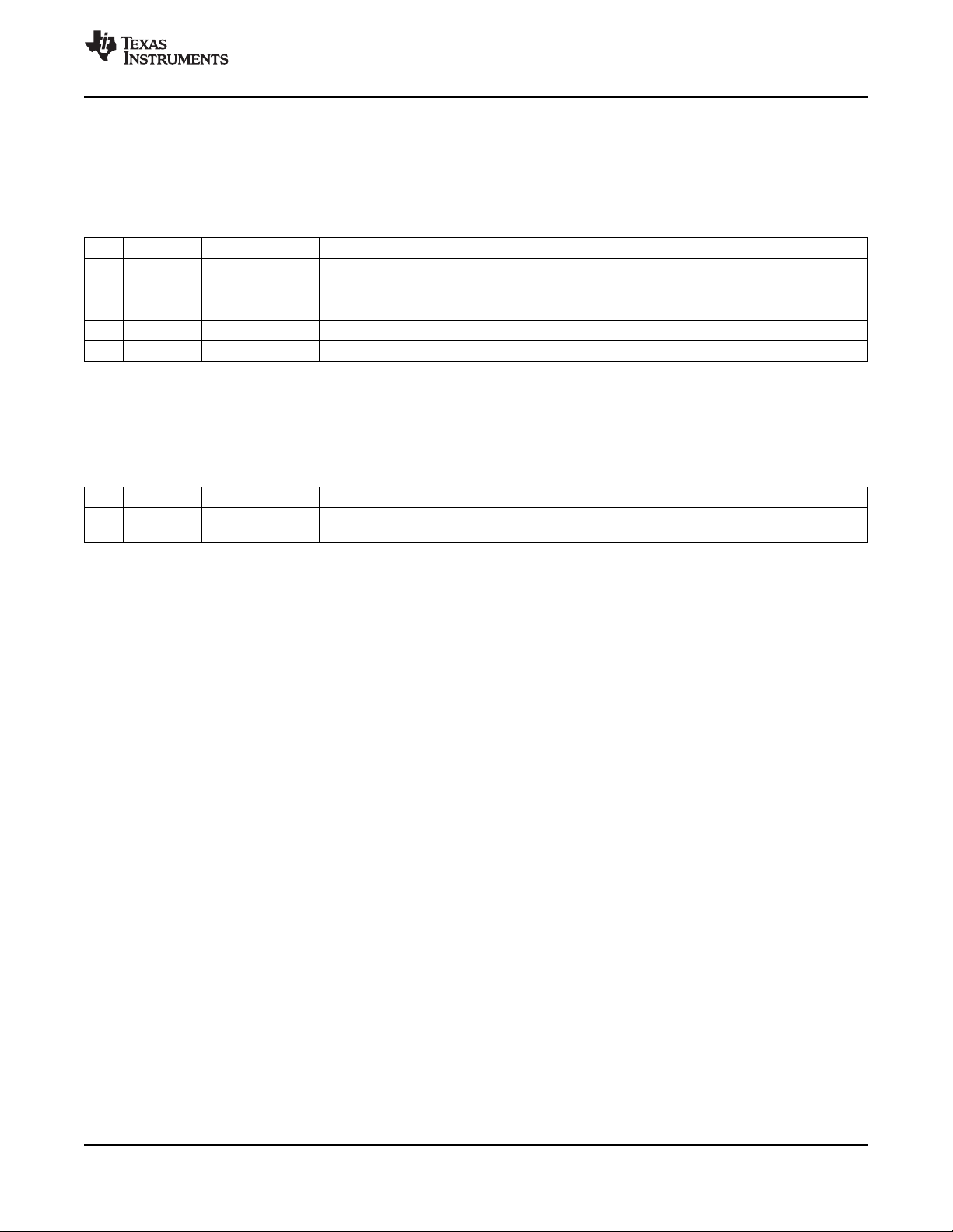
TLK100
www.ti.com
SLLS931–AUGUST 2009
6.2 Register Control Register (REGCR)
This register contains the device address to be written to access the extended registers. Write 0x1F into
bits 4:0 of this register. It also contains selection bits for auto increment of the data register.
Table 6-12. Register Control Register (REGCR), address 0x000D
BIT BIT NAME DEFAULT DESCRIPTION
15:1 Function 0, RW 00 = Address
4 01 = Data, no post increment
13:5 RESERVED 0, RO RESERVED: Writes ignored, read as 0.
4:0 DEVAD 0, RW Device Address
10 = Data, post increment on read and write
11 = Data, post increment on write only
6.3 Address or Data Register (ADDAR)
This is the address/data register.
Table 6-13. Data Register (ADDAR), address 0x000E
BIT BIT NAME DEFAULT DESCRIPTION
15:0 Addr/data 0, RW If REGCR register 15:14 = 00, holds the MMD DEVAD's address register, otherwise holds the
MMD DEVAD's data register
Copyright © 2009, Texas Instruments Incorporated Register Block 39
Submit Documentation Feedback
Product Folder Link(s): TLK100

TLK100
SLLS931–AUGUST 2009
6.4 Extended Registers
6.4.1 PHY Control Register (PHYCR)
This register provides quick access to commonly accessed PHY control information.
Table 6-14. PHY Control Register (PHYCR), address 0x0010
BIT BIT NAME DEFAULT DESCRIPTION
15:14 TX FIFO Depth 0x1,RW 00 = 4 nibbles
13:12 Reserved 0,RO Ignore on read
11 Reserved 0,RO Ignore on read
10 Force Link Good 0,RW 1 = Force link_ctrl_en10/100 according to selected speed in register 0x0
9:8 Power Down 00,RW 00 = Normal mode
Mode
7 Reserved 0,RW Reserved
6 Auto MDI-X SOR,RW 1 = Enable automatic crossover
Enable
5 Manual MDI-X 0,RW 0 = Manual MDI configuration
Mode
4 Disable PLL 0,RW 1 = Disable PLL
3:1 Reserved 0,RO Ignore on read
0 Disable Jabber 0,RW 1 = Disable Jabber function
01 = 5 nibbles
10 = 6 nibbles
11 = 8 nibbles
0 = Do Normal operation
01 = General Power Down mode: Besides SMI module everything is powered down, if bit [4]
set to ’1’, PLL is also powered down. When PLL is powered down, Reference clock is
used.
10 = Active Sleep mode – same as passive sleep, but also send NLP every ~1.4 Sec to wake
up link-partner. Automatic power-up is done when link partner is detected.
11 = Passive Sleep Mode - Besides SMI and energy detect modules, everything is powered
down. Automatic power-up is done when link partner is detected.
Bit 11 of the BMCR register(0x00) to '1' for all of these power down modes.
0 = Disable automatic crossover
1 = Manual MDI-X configuration
0 = Enable PLL
0 = Enable Jabber function
www.ti.com
40 Register Block Copyright © 2009, Texas Instruments Incorporated
Submit Documentation Feedback
Product Folder Link(s): TLK100

TLK100
www.ti.com
6.4.2 PHY Status Register (PHYSR)
This register implements the PHY Specific Status register.
Table 6-15. PHY Status Register (PHYSR), address 0x0011
BIT NAME DEFAULT DESCRIPTION
15 Reserved 0,RO Ignore on read
14 Speed 0,RO 0 = 10Mbps
1 = 100Mbps
13 Duplex 0,RO 1 = Full duplex
0 = Half duplex
12 Page Received 0,RO, LH 1 = Page received
0 = Page not received
11 Auto-Negotiation 0,RO 1 = Auto-Negotiation completed or disabled
Complete 0 = Auto-Negotiation enabled and not completed
10 Link Status 0,RO 1 = Link is up
0 = Link is down
9 Reserved 0,RO Ignore on read
8 MDI Crossover Status 0,RO 1 = MDI-X
0 = MDI
7 Reserved 0,RO Ignore on read
6 Sleep Mode Status 0,RO 1 = Sleep
0 = Active
5:2 Reserved 0,RO Ignore on read
1 Polarity 0,RO 10BT data/nlp polarity.
"1" - positive polarity.
"0" - negative polarity.
0 Jabber 0,RO 1 = Jabber
0 = No Jabber
SLLS931–AUGUST 2009
Copyright © 2009, Texas Instruments Incorporated Register Block 41
Submit Documentation Feedback
Product Folder Link(s): TLK100

TLK100
SLLS931–AUGUST 2009
6.4.3 MII Interrupt Mask Register (MINTMR)
This register contains enables for various interrupt functions supported by TLK100.
Table 6-16. MII Interrupt Mask Register (MINTMR), address 0x0012
BIT NAME DEFAULT DESCRIPTION
15 Auto-Negotiation Interrupt Enable 0, RW 1 = Enable interrupt
0 = Disable interrupt
14 Speed Changed Interrupt Enable 0,RW 1 = Enable interrupt
0 = Disable interrupt
13 Duplex Mode Changed Interrupt 0,RW 1 = Enable interrupt
Enable 0 = Disable interrupt
12 Page Received Interrupt Enable 0,RW 1 = Enable interrupt
0 = Disable interrupt
11 Auto-Negotiation Completed Interrupt 0,RW 1 = Enable interrupt
Enable 0 = Disable interrupt
10 Link Status Changed Interrupt Enable 0,RW 1 = Enable interrupt
0 = Disable interrupt
9:8 Reserved 0,RO Ignore on read
7 FIFO Overflow/Underflow Interrupt 0,RW 1 = Enable interrupt
Enable 0 = Disable interrupt
6 MDI Crossover Changed Interrupt 0,RW 1 = Enable interrupt
Enable 0 = Disable interrupt
5 Reserved 0,RO Ignore on read
4 Sleep Mode Changed Interrupt 0,RW 1 = Enable interrupt
Enable 0 = Disable interrupt
3:2 Reserved 0,RO Ignore on read
1 Polarity Changed Interrupt Enable 0,RW 1 = Enable interrupt
0 = Disable interrupt
0 Jabber Interrupt Enable 0,RW 1 = Enable interrupt
0 = Disable interrupt
www.ti.com
42 Register Block Copyright © 2009, Texas Instruments Incorporated
Submit Documentation Feedback
Product Folder Link(s): TLK100
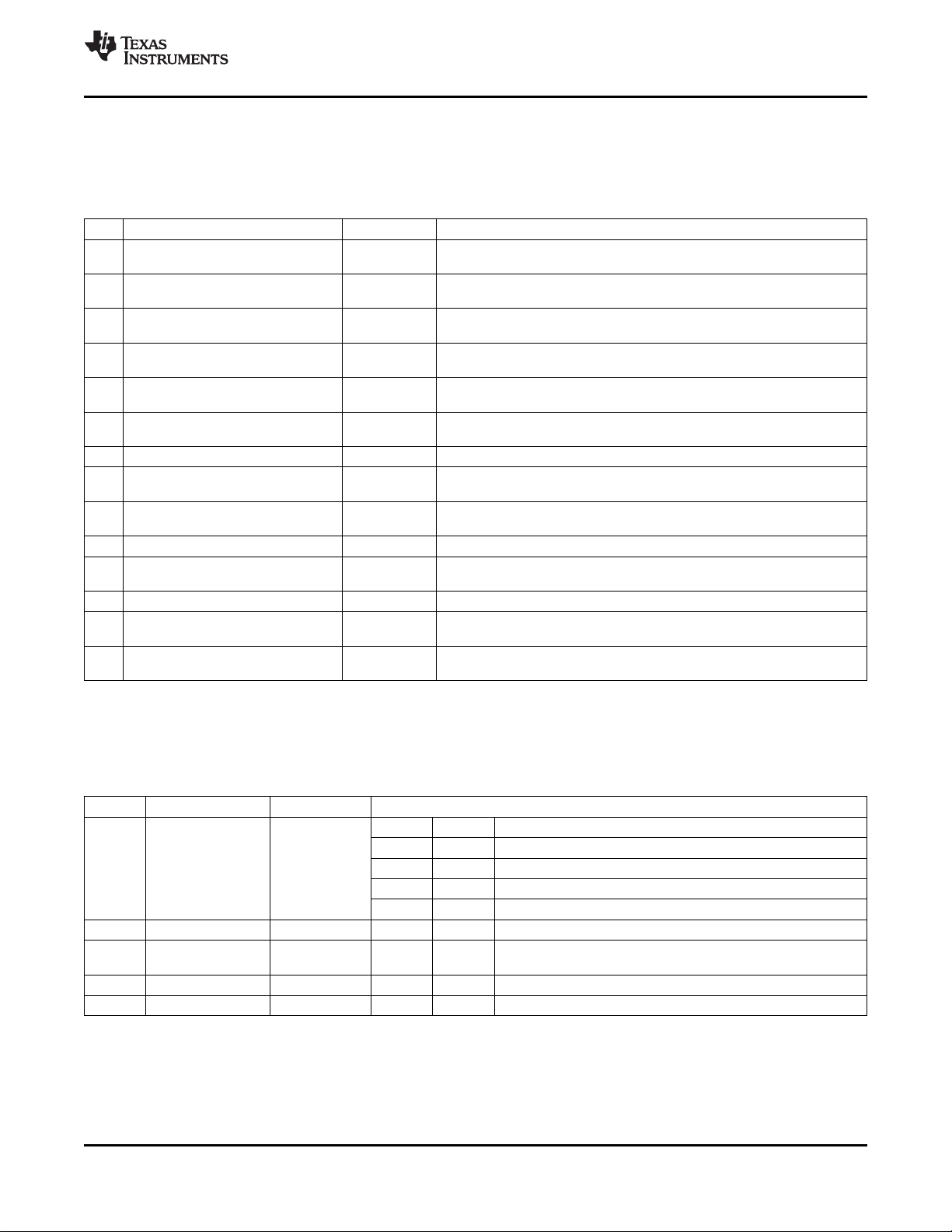
TLK100
www.ti.com
6.4.4 MII Interrupt Status Register (MINTSR)
This register gives the status of the different interrupt function supported by TLK100.
Table 6-17. MII Interrupt Status Register (MINTSR), address 0x0013
BIT NAME DEFAULT DESCRIPTION
15 Auto-Negotiation Error 0, RO, LH 1 = Auto-Negotiation error has occurred
0 = Auto-Negotiation error has not occurred
14 Speed Changed 0,RO, LH 1 = Link speed has changed
0 = Link speed has not changed
13 Duplex Mode Changed 0,RO, LH 1 = Duplex mode has changed
0 = Duplex mode has not changed
12 Page Received 0,RO, LH 1 = Page has been received
0 = Page has not been received
11 Auto-Negotiation Completed 0,RO, LH 1 = Auto-Negotiation has completed
0 = Auto-Negotiation has not completed
10 Link Status Changed 0,RO, LH 1 = Link status has changed
0 = Link status has not changed
9:8 Reserved 0,RO Ignore on read
7 FIFO Overflow/Underflow 0,RO, LH 1 = FIFO Overflow/Underflow occurred
0 = FIFO Overflow/Underflow did not occur
6 MDI Crossover Changed 0,RO, LH 1 = MDI crossover has changed
0 = MDI crossover has not changed
5 Reserved 0,RO Ignore on read
4 Sleep Mode Changed 0,RO, LH 1 = Sleep mode has changed
0 = Sleep mode has not changed
3:2 Reserved 0,RO Ignore on read
1 Polarity Changed 0,RO, LH 1 = Data polarity has changed
0 = Data polarity has not changed
0 Jabber 0,RO, LH 1 = Jabber detected
0 = Jabber not detected
SLLS931–AUGUST 2009
6.4.5 MII Interrupt Control Register (MINTCR)
This register enables to control the polarity and enabling the interrupts.
Table 6-18. MII Interrupt Control Register (MINTCR), address 0x0014
BIT NAME DEFAULT DESCRIPTION
15 INTN_OE 0,RW Bit 15 Bit 12 Pin 42 Function
0 0 Power Down
0 1 Power Down
1 0 Interrupt
1 1 Power Down
14 Reserved 0,RO Ignore on read
13 Interrupt Polarity 1,RW 1 = Interrupt pin is active low
12 INTN_OEN 1,RW Refer to the table given in the bit 15 description.
11:0 Reserved 0,RO Ignore on read
0 = Interrupt pin is active high
Copyright © 2009, Texas Instruments Incorporated Register Block 43
Submit Documentation Feedback
Product Folder Link(s): TLK100

TLK100
SLLS931–AUGUST 2009
www.ti.com
6.4.6 Receiver Error Counter Register (RECR)
This counter keeps count of the number of receive errors.
Table 6-19. Receiver Error Counter Register (RECR), address 0x0015
BIT BIT NAME DEFAULT DESCRIPTION
15:0 RX Error Count 0, RO, SC Receive errors counter (saturates in max value, clears on dummy write)
6.4.7 BIST Control Register (BISCR)
This register is used for configuring the PRBS BIST and to select the loopback point in the signal chain.
Table 6-20. BIST Control Register (BISCR), address 0x0016
BIT NAME DEFAULT DESCRIPTION
15 PRBS Count Mode 0, RW 1 = Continuous mode, when on of the PRBS counters reaches max value, pulse is
14 Generate PRBS Packets 0, RW 1 = When packet generator is enabled, generate continuous packets with PRBS data.
13 Packet Generation 64 bit 0, RW 1 = Transmit 64 byte packets in packet generation mode
mode
12 Packet Generation Enable 0, RW 1 = Enable packet/PRBS generator
11:5 Reserved 0, RO Ignore on read
4:0 Loopback Mode 0, RW Selects loop back mode:
generated and counter starts counting from zero again
0 = Single mode, When one of the PRBS counters reaches it's max value, PRBS
checker stops counting.
When packet generator is disabled, PRBS checker is still enabled.
0 = When packet generator is enabled, generate single packet with constant data.
PRBS gen/check is disabled.
0 = Transmit 1518 byte packets in packet generation mode
0 = Disable packet/PRBS generator
Near-end Loopbacks
[00001] – MII Loopback
[00010] – PCS Loopback (In 100BaseTX only)
[00100] – Digital Loopback
[01000] – Analog Loopback (requires 100Ω termination)
Far-end Loopback:
[10000] – Reverse Loopback
6.4.8 BIST STATUS Register (BISSR)
This register gives the status of the PRBS test and the sleep mode of the core.
Table 6-21. BIST STATUS Register (BISSR), address 0x0017
BIT NAME DEFAULT DESCRIPTION
15:12 Reserved 0,RO Ignore on read
11 PRBS Locked 0,RO 1 = PRBS checker is locked on received byte stream
10 PRBS Sync Loss 0,RO,LH 1 = PRBS checker has lost sync
9 Packet Generator Busy 0,RO 1 = Packet generator is in process
8 Core Power Mode 0,RO 1 = Core is in normal power mode
Status 0 = Core is powered down or in sleep mode
7:0 Reserved 0,RO Ignore on read
44 Register Block Copyright © 2009, Texas Instruments Incorporated
0 = PRBS checker is not locked
0 = PRBS checker has not lost sync
0 = Packet generator is not in process
Submit Documentation Feedback
Product Folder Link(s): TLK100

TLK100
www.ti.com
SLLS931–AUGUST 2009
6.4.9 BIST Byte Count Register (BISBCR)
This register gives the total number of bytes received by the PRBS checker.
Table 6-22. BIST Count Register (BISBCR), address 0x0071
BIT BIT NAME DEFAULT DESCRIPTION
15:0 prbs_byte_cnt 0, RO Holds number of total bytes that received by the PRBS checker. Value in this register is locked
when write is done to register 0x0072 bit[0] or bit[1]. When PRBS Count Mode set to zero,
count stops on 0xFFFF (see register 0x0016)
6.4.10 BIST Error Count Register (BISECR)
This register gives the total number of error bytes that was received by the PRBS checker.
Table 6-23. BIST Error Count Register (BISECR), address 0x0072
BIT BIT NAME DEFAULT DESCRIPTION
15:8 Reserved 0, RO Ignore on read
7:0 prbs_err_cnt 0, RO Holds number of erroneous bytes received by the PRBS checker. Value in this register is
locked when write is done to bit[0] or bit[1] (see below).
When PRBS Count Mode set to zero, count stops on 0xFF (see register 0x0016)
Notes:
Writing bit 0 generates a lock signal for the PRBS counters
Writing bit 1 generates a lock and clear signal for the PRBS counters
6.4.11 BIST Packet Length Register (BISPLR)
This register allows programming the length of the PRBS packet in bytes.
Table 6-24. BIST Packet Length Register (BISPLR), address 0x007B
BIT BIT NAME DEFAULT DESCRIPTION
15:0 Cfg_pkt_len_prbs 0X5DC,RW Length of PRBS packets in bytes
6.4.12 BIST Inter Packet Gap Register (BISIPGR)
This register allows programming the inter packet gap, in bytes, between the PRBS packets.
Table 6-25. BIST Inter Packet Gap Register (BISIPGR), address 0x007C
BIT BIT NAME DEFAULT DESCRIPTION
15:0 Cfg_ipg_len 0X7D,RW Inter-packet gap (in bytes) between PRBS packets
Copyright © 2009, Texas Instruments Incorporated Register Block 45
Submit Documentation Feedback
Product Folder Link(s): TLK100

TLK100
SLLS931–AUGUST 2009
6.4.13 LED Direct Control Register (LEDCR)
This register provides the ability to directly control any or all LED outputs. The polarity, pulse width and
blink rates can be programmed using this register.
Table 6-26. LED Direct Control Register (LEDCR), address 0x0018
BIT NAME DEFAULT DESCRIPTION
15 LEDs Enable 1,RW 1 = Enable LEDs
0 = Disable LEDs
14:13 Pulse Width 0x2,RW 00 = 50mSec
01 = 100mSec
10 = 200mSec
11 = 500mSec
12 Force Interrupt 0,RW 1 = Assert interrupt pin
0 = Normal interrupt mode
11:10 Reserved 0,RO Ignore on read
9:8 Blink Rate 0x2,RW 00 = 20Hz (50mSec)
01 = 10Hz (100mSec)
10 = 5Hz (200mSec)
11 = 2Hz (500mSec)
7 Reserved 0,RO Ignore on read
6:5 LED Mode 0,SOR,RW 01 = Mode1
00 = Mode2
10 = Mode3
4:3 Reserved 0,RO Ignore on read
2 LED ACT Polarity SOR,RW 0 = Active low
1 = Active high
1 LED SPEED Polarity SOR,RW 0 = Active low
1 = Active high
0 LED LINK Polarity SOR,RW 0 = Active low
1 = Active high
www.ti.com
6.4.14 Power Down Register (PDR)
This register provides control for doing a software reset of the PHY.
Table 6-27. Power Down Register (PDR), address 0x001F
BIT NAME DEFAULT DESCRIPTION
15 Software Global 0,RW,SC 1 = Reset PHY (Same effect as in hardware reset, including registers reset)
Reset 0 = Normal mode
14:0 Reserved 0,RO Always write zero
46 Register Block Copyright © 2009, Texas Instruments Incorporated
Submit Documentation Feedback
Product Folder Link(s): TLK100

TLK100
www.ti.com
SLLS931–AUGUST 2009
6.4.15 False Carrier Sense Counter Register (FCSCR)
This register counts the error nibbles between the IDLE nibbles (BAD_SSD), in nibble time. This count
register is reset when this register is read.
Table 6-28. False Carrier Sense Counter Register (FCSCR), address 0x0042
BIT BIT NAME DEFAULT DESCRIPTION
15:8 RESERVED 0, RO Ignore on read
7:0 idle_err_count_100 0, RO IDLE error counter value. Counts received error nibbles between IDLE nibbles (BAD_SSD), in
nibble time.
Note: Reading this register clears the idle_err_count_100 counter
6.4.16 RX Channel Control Register (RXCCR)
This register allows configuration of RX channel. By programming bits 3,2 of this register to ‘1’ the
channels can be mirrored.
Table 6-29. RX Channel Control Register (RXCCR), address 0x0070
BIT NAME DEFAULT FUNCTION
15:4 Reserved 0,RO Ignore on read
3 Polarity_inv 0,RW When 1 Change the polarity of:
2 Mdix 0,RW 1 = MDIX
1:0 Reserved 0,RW Always write 0
1 = Polarity of RD and TD is inverted
0 = Polarity of RD and TD is not inverted
0 = MDI
6.5 Cable Diagnostic Registers
6.5.1 Cable Diagnostic Registers (CDCR)
This register is used to select the channel for which cable diagnostics test needs to be done. It has the
enable bits for the diagnostic tests and also allows one to choose which TDR peak and location will be
written to the CDRR register (0x001C).
Table 6-30. Cable Diagnostic Registers (CDCR), address 0x001A
BIT NAME DEFAULT DESCRIPTION
15:14 Reserved 0,RW, SC Always 0
13 ALCD/DSA Test 0,RW, SC 1 = Start ALCD/DSA test.
Start 0 = Do not start ALCD/DSA test
12 TDR Test Start 0,RW, SC 1 = Start TDR test
11 Reserved 0,RO Reserved
10:8 Cable Diagnostics 0,RW Selects the output of register 0x1C as follows:
Result Select 0: {TDR peak 0 amplitude, TDR peak 0 location}
8:1 Reserved 0,RO Ignore on read
0 Channel Select 0,RW Selects channel for Cable Diagnostics Test
0 = Do not start TDR test
1: {TDR peak 1 amplitude, TDR peak 1 location}
2: {TDR peak 2 amplitude, TDR peak 2 location}
3: {TDR peak 3 amplitude, TDR peak 3 location}
4: {TDR peak 4 amplitude, TDR peak 4 location}
6: ALCD Length
0 = TD±
1 = RD±
Copyright © 2009, Texas Instruments Incorporated Register Block 47
Submit Documentation Feedback
Product Folder Link(s): TLK100
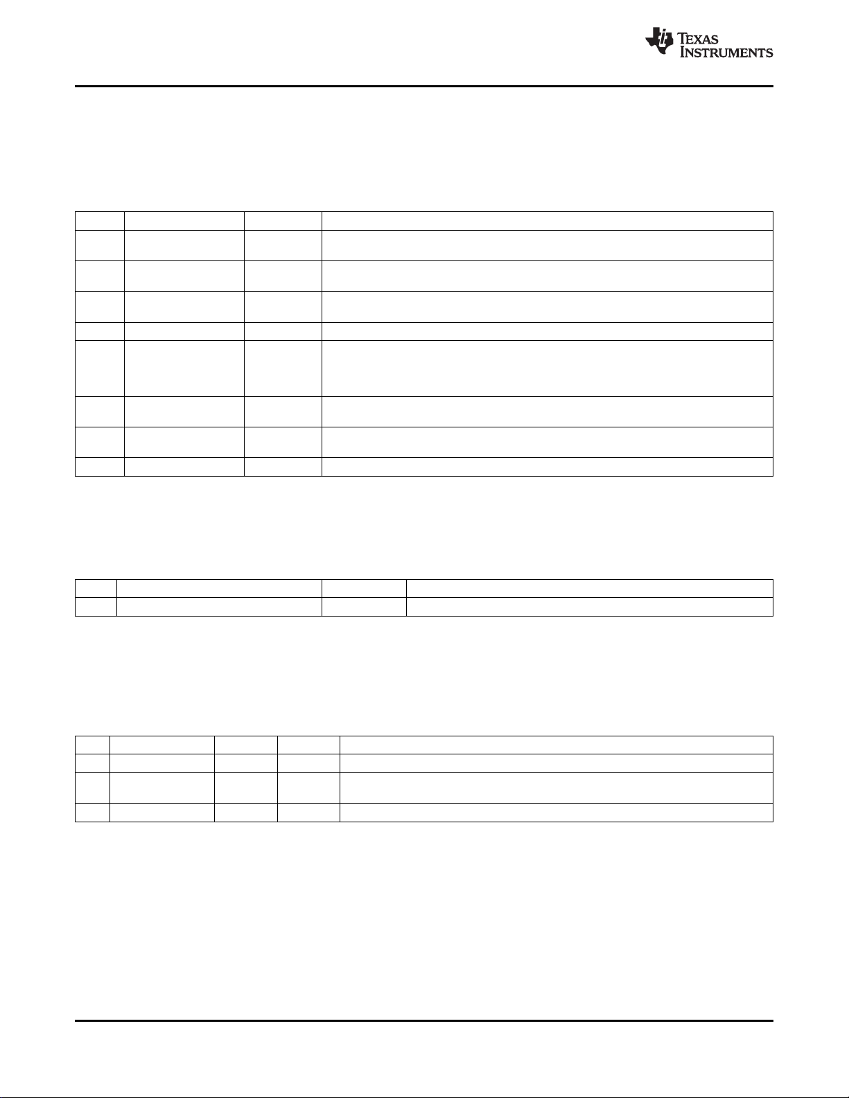
TLK100
SLLS931–AUGUST 2009
6.5.2 Cable Diagnostic Status Register (CDSR)
This register gives the status of the cable diagnostic tests. It also allows configuring different modes of the
ALCD and DSA tests.
Table 6-31. Cable Diagnostic Status Register (CDSR), address 0x001B
BIT NAME DEFAULT DESCRIPTION
15 ALCD/DSA Done 0,RO 1 = ALCD/DSA is done
0 = ALCD/DSA is not done
14 TDR Fail 1,RO 1 = TDR has failed
0 = TDR has not failed
13 TDR Done 0,RO 1 = TDR is done
0 = TDR is not done
12:10 Reserved 0x4,RO Ignore on read
9:6 DSA Input Signal 7,RW 7 = ALCD
5 = DSA Adaptive data mode
3 = DSA Raw data mode
Others are reserved
5 DSA Enable 0,RW 1 = DSA Engine is enabled
0 = DSA Engine is disabled
4 ALCD/DSA mode 1,RW 1 = DSA Raw data mode
0 = ALCD/DSA Adaptive data mode
3:0 Reserved 0,RO Ignore on read
www.ti.com
6.5.3 Cable Diagnostic Results Register (CDRR)
This register gives the result of the cable diagnostic tests. The software will post process this result.
Table 6-32. Cable Diagnostic Results Register (CDRR), address 0x001C
BIT BIT NAME DEFAULT DESCRIPTION
15:0 Cable Diagnostics Result Register 0, RO As specified in register 0x1A bits [11:8]
6.5.4 TDR State Machine Enable (TDRSMR)
This register allows configuration of the TDR state machines. Only when the bits 15, 14 of this register are
set to ‘1’ the registers 0x0090 and 0x0094 can be used.
Table 6-33. TDR State Machine Enable Register (TDRSMR), address 0x0080
BIT NAME TYPE RESET FUNCTION
15 cmn_tdr_sm_mode RW 0 1 = Configure TDR state machine mode. This bit is cleared when TDR is complete
14 cmn_tdr_tx_sm_m RW 0 1 = Configure TDR transmit state machine mode. This bit is cleared when the TDR is
ode complete.
13:0 Reserved RW 0 Reserved
48 Register Block Copyright © 2009, Texas Instruments Incorporated
Submit Documentation Feedback
Product Folder Link(s): TLK100

TLK100
www.ti.com
6.5.5 TDR Pattern Amplitude Register (TDRPAR)
This register allows to program the pattern used to generate the TDR pulses. Bits 4:0 of this register give
the amplitude of the TDR pulse. A value of 0x8 maps to an amplitude of 1V. For values from 0x8 to 0xF
the amplitude is saturated to 1V. The TDR pattern is 16 symbols long. So, sixteen consecutive writes to
this register are required. The value of these bits for each write determines the amplitude for that symbol.
Each symbol is 8ns wide. For this register to function, the bits 15,14 of TDRSMR register (0x0080) should
be set to ‘1’
Table 6-34. TDR Pattern Amplitude Register (TDRPAR), address 0x0090
BIT NAME DEFAULT FUNCTION
15:5 Reserved 0,RO Ignore on read
4:0 tdr_pattern_din_config 0,RW Configure TDR Transmit Pattern.
6.5.6 TDR Manual Pulse Register (TDRMPR)
This register allows to program a manual TDR pulse. When bit 1 of this register is set then the pattern
programmed in the TDRPAR register is put on the TD line. If the TDRPAR register is not programmed
then a default TDR pulse is put on the TD line. It is NOT used for TDR measurements.
Table 6-35. TDR Manual Pulse Register (TDRMPR), address 0x0094
BIT NAME DEFAULT FUNCTION
15:2 Reserved 0,RO Ignore on read
1 tdr_tx_start 0,RW 1 = Start TDR pattern transmission
0 = Do not start TDR pattern transmission
0 Reserved 0x0,RW Reserved
SLLS931–AUGUST 2009
6.5.7 TDR Channel Silence Register (TDRCSR)
This register allows programming of the TDR channel silence timers.
Table 6-36. TDR Channel Silence Register (TDRCSR), address 0x0C00
BIT NAME DEFAULT FUNCTION
15:14 Reserved 0,RO Ignore on read
13:12 cfg_link_down_timer 0x2,RW Hold time, to make sure the link failed:
11:10 cfg_post_silence_time 0x1,RW The needed silence time after the TDR test:
9:8 cfg_pre_silence_time 0x1,RW The needed silence time before the TDR test:
7:0 cfg_silence_th 0xC8,RW Energy calculator threshold value, to break silence.
0x0 – no hold time.
0x1 – 500ms hold time.
0x2 – 1s hold time.
0x3 – 2s hold time.
0x0 – no silence needed.
0x1 – 10ms of silence.
0x2 – 100ms of silence.
0x3 – 1s of silence.
0x0 – no silence needed.
0x1 – 10ms of silence.
0x2 – 100ms of silence.
0x3 – 1s of silence.
Copyright © 2009, Texas Instruments Incorporated Register Block 49
Submit Documentation Feedback
Product Folder Link(s): TLK100

TLK100
SLLS931–AUGUST 2009
6.5.8 TDR Control Register (TDRCR)
This register allows configuring the TDR modes.
Table 6-37. TDR Control Register (TDRCR), address 0x0C01
BIT NAME DEFAULT FUNCTION
15:11 Reserved 0x02,RO Ignore on read
10 cfg_tdr_tx_mode 0x1,RW 1 – Enable TDR TX transmission mode
9 Reserved 0,RW Reserved
8:6 cfg_soft_avr_cycles 0x7,RW Number of averaging cycles:
0x0 – TDR disabled.
0x1 – 1 TDR cycle (no averaging).
0x2 – 2 TDR cycles.
0x3 – 4 TDR cycles.
0x4 – 8 TDR cycles.
0x5 – 16 TDR cycles.
0x6 – 32 TDR cycles.
0x7 – 64 TDR cycles.
5:3 cfg_post_cmp_size 0x4,RW Number of forward samples for peak detection comparison.
2:0 cfg_pre_cmp_size 0x3,RW Number of backward samples for peak detection comparison.
6.5.9 TDR Clock Cycles Register (TDRLCR)
This register allows configuring the number of clock cycles in a pattern TDR test.
www.ti.com
Table 6-38. TDR Clock Cycles Register (TDRLCR), address 0x0C02
BIT NAME DEFAULT FUNCTION
15:8 Reserved 0,RO Ignore on read
7:0 cfg_ptrn_cycle_time 0xFF,RW Number of clock cycles in a TDR pattern test.
6.5.10 TDR Low Threshold Register (TDRLT1)
This register allows configuring the threshold for finding the peaks of the reflected signal in the TDR test.
Table 6-39. TDR Low Threshold Register (TDRLT1), address 0x0C03
BIT NAME DEFAULT FUNCTION
15 Reserved 0,RO Ignore on read
14:8 cfg_ptrn_low_th_1 0xC,RW Peak (absolute) low threshold value 1, for TX pattern.
7 Reserved 0,RO Ignore on read
6:0 cfg_ptrn_low_th_0 0x10,RW Peak (absolute) low threshold value 0, for TX pattern.
6.5.11 TDR Low Threshold Register (TDRLT2)
This register allows configuring the threshold for finding the peaks of the reflected signal in the TDR test.
Table 6-40. TDR Low Threshold Register (TDRLT2), address 0x0C04
BIT NAME DEFAULT FUNCTION
15 Reserved 0,RO Ignore on read
14:8 cfg_ptrn_low_th_3 0x7,RW Peak (absolute) low threshold value 3, for TX pattern.
7 Reserved 0,RO Ignore on read
6:0 cfg_ptrn_low_th_2 0x9,RW Peak (absolute) low threshold value 2, for TX pattern.
50 Register Block Copyright © 2009, Texas Instruments Incorporated
Submit Documentation Feedback
Product Folder Link(s): TLK100

TLK100
www.ti.com
6.5.12 TDR Low Threshold Register (TDRLT3)
This register allows configuring the threshold for finding the peaks of the reflected signal in the TDR test.
Table 6-41. TDR Low Threshold Register (TDRLT3), address 0x0C05
BIT NAME DEFAULT FUNCTION
15 Reserved 0,RO Ignore on read
14:8 cfg_ptrn_low_th_5 0x4,RW Peak (absolute) low threshold value 5, for TX pattern.
7 Reserved 0,RO Ignore on read
6:0 cfg_ptrn_low_th_4 0x5,RW Peak (absolute) low threshold value 4, for TX pattern.
6.5.13 TDR Low Threshold Register (TDRLT4)
This register allows configuring the threshold for finding the peaks of the reflected signal in the TDR test.
Table 6-42. TDR Low Threshold Register (TDRLT4), address 0x0C06
BIT NAME DEFAULT FUNCTION
15 Reserved 0,RO Ignore on read
14:8 cfg_ptrn_low_th_7 0x3,RW Peak (absolute) low threshold value 7, for TX pattern.
7 Reserved 0,RO Ignore on read
6:0 cfg_ptrn_low_th_6 0x3,RW Peak (absolute) low threshold value 6, for TX pattern.
SLLS931–AUGUST 2009
6.5.14 TDR High Threshold Register (TDRHT1)
This register allows configuring the threshold for finding the peaks of the reflected signal in the TDR test.
Table 6-43. TDR High Threshold Register (TDRHT1), address 0x0C07
BIT NAME DEFAULT FUNCTION
15 Reserved 0,RO Ignore on read
14:8 cfg_ptrn_High_th_1 0x53,RW Peak (absolute) High threshold value 1, for TX pattern.
7 Reserved 0,RO Ignore on read
6:0 cfg_ptrn_High_th_0 0x53,RW Peak (absolute) High threshold value 0, for TX pattern.
Copyright © 2009, Texas Instruments Incorporated Register Block 51
Submit Documentation Feedback
Product Folder Link(s): TLK100

TLK100
SLLS931–AUGUST 2009
6.5.15 TDR High Threshold Register (TDRHT2)
This register allows configuring the threshold for finding the peaks of the reflected signal in the TDR test.
Table 6-44. TDR High Threshold Register (TDRHT2), address 0x0C08
BIT NAME DEFAULT FUNCTION
15 Reserved 0,RO Ignore on read
14:8 cfg_ptrn_High_th_3 0x4A,RW Peak (absolute) High threshold value 3, for TX pattern.
7 Reserved 0,RO Ignore on read
6:0 cfg_ptrn_High_th_2 0x53,RW Peak (absolute) High threshold value 2, for TX pattern.
6.5.16 TDR High Threshold Register (TDRHT3)
This register allows configuring the threshold for finding the peaks of the reflected signal in the TDR test.
Table 6-45. TDR High Threshold Register (TDRHT3), address 0x0C09
BIT NAME DEFAULT FUNCTION
15 Reserved 0,RO Ignore on read
14:8 cfg_ptrn_High_th_5 0x2F,RW Peak (absolute) High threshold value 5, for TX pattern.
7 Reserved 0,RO Ignore on read
6:0 cfg_ptrn_High_th_4 0x3A,RW Peak (absolute) High threshold value 4, for TX pattern.
www.ti.com
6.5.17 TDR High Threshold Register (TDRHT4)
This register allows configuring the threshold for finding the peaks of the reflected signal in the TDR test.
Table 6-46. TDR High Threshold Register (TDRHT4), address 0x0C0A
BIT NAME DEFAULT FUNCTION
15 Reserved 0,RO Ignore on read
14:8 cfg_ptrn_High_th_7 0x1F,RW Peak (absolute) High threshold value 7, for TX pattern.
7 Reserved 0,RO Ignore on read
6:0 cfg_ptrn_High_th_6 0x26,RW Peak (absolute) High threshold value 6, for TX pattern.
6.5.18 TDR Pattern Control Register 1 (TDRLCR1)
This register allows configuring the forward shadow values for the TDR test.
Table 6-47. TDR Pattern Control Register 1 (TDRLCR1), address 0x0C0B
BIT NAME DEFAULT FUNCTION
15:12 Reserved 0,RO Ignore on read
11:9 cfg_ptrn_fr_shdw_inc 0x1,RW Forward shadow area from peak detection increment factor (X/128).
8:5 cfg_ptrn_init_fr_shdw 0x6,RW Forward shadow area from peak detection initial samples size.
4:0 cfg_ptrn_init_skip 0x10, RW Initial skip (ignore) samples number from Tx start.
52 Register Block Copyright © 2009, Texas Instruments Incorporated
Submit Documentation Feedback
Product Folder Link(s): TLK100

TLK100
www.ti.com
6.5.19 TDR Pattern Control Register 2 (TDRLCR2)
This register allows configuring the gear threshold values for the TDR test.
Table 6-48. TDR Pattern Control Register 2 (TDRLCR2), address 0x0C0C
BIT NAME DEFAULT FUNCTION
15:9 Reserved 0,RO Ignore on read
8:4 cfg_ptrn_gear_tout 0x14,RW Thresholds gear shifts distance in samples
3:0 Reserved 0x8,RO Ignore on read
6.5.20 DSA Configuration Register 1 (DSACR1)
This register allows use of the smoothing filter during the DSA tests.
Table 6-49. DSA Configuration Register 1 (DSACR1), address 0x0C26
BIT NAME DEFAULT FUNCTION
15:7 Reserved 0x180,RO Ignore on read
6 cfg_dsa_smooth_filt_byps 0x1,RW 0 = Disable DSA engine smooth filter bypass
1 = Enable DSA engine smooth filter bypass
5:0 Reserved 0x04,RO Ignore on read
6.5.21 DSA Configuration Register 2 (DSACR2)
SLLS931–AUGUST 2009
This register allows configuration of the DSA taps are used for the DSA tests. We specify the first and last
taps in use and the DSA uses all the taps between them.
Table 6-50. DSA Configuration Register 2 (DSACR2), address 0x0C27
BIT NAME DEFAULT FUNCTION
15:8 cfg_dsa_en_last_coeff_num 0x1E,RW Last coefficient number used by the DSA engine
7:0 cfg_dsa_en_first_coeff_num 0x0,RW First coefficient number used by the DSA engine
6.5.22 DSA Start Frequency (DSASFR)
This register allows configuration of the starting frequency for the spectrum analysis of the DSA engine. It
represents 1.9 kHz resolution in the frequency domain.
Table 6-51. DSA Start Frequency (DSASFR), address 0x0C28
BIT NAME DEFAULT FUNCTION
15:0 cfg_start_freq 0x0,RW Starting frequency for the DSA
6.5.23 DSA Frequency Control (DSAFCR)
This register defines the average factor we will use in the DSA. In addition it defines the frequency step for
the DSA. The field represents resolution of 119.2 Hz.
Table 6-52. DSA Frequency Control (DSAFCR), address 0x0C29
BIT NAME DEFAULT FUNCTION
15:12 cfg_dsa_average 0xA,RW Averaging factor for DSA engine – 2X cycles
11 Reserved 0x0,RO Reserved
10:0 cfg_dsa_inc_factor 0x400,RW DSA Frequency increment factor (frequency step)
Copyright © 2009, Texas Instruments Incorporated Register Block 53
Submit Documentation Feedback
Product Folder Link(s): TLK100

TLK100
SLLS931–AUGUST 2009
6.5.24 DSA Output Control (DSAOCR)
This register configures which DSA outputs are selected to the 16 bit RAM available bits. The files
configure the MSB location of the DSA engine.
Table 6-53. DSA Output Control (DSAOCR), address 0x0C2A
BIT NAME DEFAULT FUNCTION
15:12 cfg_dsa_output_msb 0x0,RW DSA output MSB select. Select which bits of the DSA output are saved in the
RAM
11:0 Reserved 0x003,RO Reserved
6.5.25 RAM Control 1 (RAMCR1)
This register enables the RAM in order to read the DSA results.
Table 6-54. RAM Control 1 (RAMCR1), address 0x0D00
BIT NAME DEFAULT FUNCTION
15 cpu_ram_en 0x0,RW 1 = Enable CPU access to RAM
0 = Disable CPU access to RAM
14:0 Reserved 0x0,RO Reserved
6.5.26 RAM Control 2 (RAMCR2)
www.ti.com
This register enables resetting the RAM memory and address prior to starting the DSA test
Table 6-55. RAM Control 2 (RAMCR2), address 0x0D01
BIT NAME DEFAULT FUNCTION
15 man_cable_diag_restart 0x0,RW 1= Restart cable diagnostics block manual
14 man_cable_diag_reset 0x0,RW 1= Soft reset of cable diagnostics block manual
13 reset_ram_addr_indx 0x0,RW 1= Reset RAM address index
12:0 Reserved 0x0,RO Reserved
0 = Do not restart cable diagnostics block manual
0 = Do not reset cable diagnostics block manual
0 = Do not reset RAM address index
6.5.27 RAM Data Out (RAMDR)
This register is the DSA output result register.
Table 6-56. RAM Data Out (RAMDR), address 0x0D04
BIT NAME DEFAULT FUNCTION
15:0 RAM Data Out 0x0,RW RAM data out
6.5.28 CD Pre Test Configuration Control 1 (CDPTC1R)
This register enables cable diagnostic pre test configuration.
Table 6-57. CD Pre Test Configuration Control 1 (CDPTC1R), address 0x0107
BIT NAME DEFAULT FUNCTION
15:9 Reserved 0x0,RO Reserved
8 cd_pre_test_cfg_en 0,RW 1 = Enable Cable diagnostic pre test configuration
7:0 Reserved 0,RO Reserved
54 Register Block Copyright © 2009, Texas Instruments Incorporated
0 = Disable Cable diagnostic pre test configuration
Submit Documentation Feedback
Product Folder Link(s): TLK100
TLK100
www.ti.com
6.5.29 CD Pre Test Configuration Control 2 (CDPTC2R)
This register latches the outcome of enabling the cable diagnostic pre test configuration.
Table 6-58. CD Pre Test Configuration Control 2 (CDPTC2R), address 0x010F
BIT NAME DEFAULT FUNCTION
15:4 Reserved 0x034,RO Reserved
3 cd_pre_test_cfg_latched 0,RW 1 = Cable Diagnostic pre test configuration is latched
0 = Cable Diagnostic pre test configuration is not latched
2:0 Reserved 0,RO Reserved
6.5.30 LPF Bypass (LPFBR)
This register enables to bypass the LPF for the DSA tests.
Table 6-59. LPF Bypass (LPFBR), address 0x00AC
BIT NAME DEFAULT FUNCTION
15:11 Reserved 0x0,RO Reserved
10 dsa_lpf_bypass 0,RW 1 = Bypass DSA LPF
0 = Do not bypass DSA LPF
9:0 Reserved 0,RO Reserved
SLLS931–AUGUST 2009
Copyright © 2009, Texas Instruments Incorporated Register Block 55
Submit Documentation Feedback
Product Folder Link(s): TLK100

TLK100
SLLS931–AUGUST 2009
www.ti.com
7 Electrical Specifications
All parameters are derived by test, statistical analysis, or design.
7.1 ABSOLUTE MAXIMUM RATINGS
VDD33_IO, VDD33_VA11, Supply voltage –0.3 to 3.8 V
VDD33_V18, VDD33_VD11
V18_PFBIN1, V18_PFBIN2 –0.3 to 2.2 V
VA11_PFBIN1, VA11_PFBIN2 –0.3 to 1.8 V
XI DC Input voltage –0.3 to 2.2 V
TD-, TD+, RD-, RD+ –0.3 to 6 V
Other Inputs –0.3 to 3.8 V
XO DC Output voltage –0.3 to 2.2 V
Other outputs –0.3 to 3.8 V
Maximum die temperature θ
ESD
(1) Stresses beyond those listed under “absolute maximum ratings” may cause permanent damage to the device. These are stress ratings
only, and functional operation of the device at these or any other conditions beyond those indicated under “recommended operating
conditions” is not implied. Exposure to absolute-maximum-rated conditions for extended periods may affect device reliability.
(2) On pins TD+, TD-, RD+, RD-, VDD33_IO, VDD33_VA11 VDD33_V18, VDD33_VD11, V18_PFBIN1, V18_PFBIN2, VA11_PFBIN1,
VA11_PFBIN2, VA11_PFBOUT, V18_PFBOUT, VDD11, VSS.
J
IEC 60749-26 ESD (human-body model)
JEDEC Standard 22, Test Method A114 (human-body model)
JEDEC Standard 22, Test Method A114 (human-body model), all pins 1.5
JEDEC Standard 22, Test Method C101 (charged-device model), all pins 1.5
(1)
VALUE UNIT
105 °C
(2)
(2)
±16 kV
±16
7.2 THERMAL CHARACTERISTICS
over operating free-air temperature range (unless otherwise noted)
PARAMETER MIN TYP MAX UNIT
θ
JA
θ
JB
θ
JC
Junction-to-ambient thermal resistance (no airflow) 26.8
Junction-to-board thermal resistance 16.2 °C/W
Junction-to-case thermal resistance 40
7.3 RECOMMENDED OPERATING CONDITIONS
MIN NOM MAX UNIT
VDD33_VA11,VDD33_V18, Core Supply voltage 2.38 3.3 3.6 V
VDD33_VD11
VDD33_IO I/O 3.3V Supply 3.0 3.3 3.6 V
V18_PFBIN1, External Supply
V18_PFBIN2
VA11_PFBIN1, 1.04 1.1 1.15 V
VA11_PFBIN2
T
A
P
D
Ambient temperature
Power dissipation
(1) When the internal voltage regulator is not used and the external supply is used
(2) Provided that GNDPAD, pin 49, is soldered down. See Thermal Vias Recommendation for more detail.
(3) For 100Base-TX, When external 1.8V, 1.1 and 3.3V supplies are used.
(1)
(2)
(3)
1.7 1.8 1.9 V
–40 85 °C
189 mW
56 Electrical Specifications Copyright © 2009, Texas Instruments Incorporated
Submit Documentation Feedback
Product Folder Link(s): TLK100

TLK100
www.ti.com
SLLS931–AUGUST 2009
7.4 DC CHARACTERISTICS
over operating free-air temperature range (unless otherwise noted)
PARAMETER TEST CONDITIONS MIN TYP MAX UNIT
V
IH
V
IL
I
IH
I
IL
V
OL
V
OH
I
OZ
V
TPTD_100
V
TPTDsym
V
TPTD_10
C
IN1
Input high voltage
Input low voltage
Input high current VIN= V
Input low current VIN= GND 10 μA
Output low voltage IOL= 4 mA 0.4 V
Output high voltage IOH= –4 mA VCC– 0.5 V
3-State leakage V
100M transmit voltage 0.95 1 1.05 V
100M transmit voltage symmetry ±2%
10M transmit voltage 2.2 2.5 2.8 V
CMOS input capacitance 5 pF
COUT1 CMOS output capacitance 5 pF
SD
SD
V
THon
THoff
TH1
100BASE-TX Signal detect turnon threshold 1000
100BASE-TX Signal detect turnoff threshold 200
10BASE-T Receive threshold 585 mV
(1) Nominal VCCof VDD33_IO = 3.3V
(1)
(1)
CC
OUT
= VCC, V
= GND ±10 μA
OUT
2.0 V
0.8 V
10 μA
mV diff
pk-pk
mV diff
pk-pk
7.5 POWER SUPPLY CHARACTERISTICS
The data was measured from a TLK100 evaluation board. The current from each of the power supply is
measured and the power dissipation is computed. For the single 3.3V external supply case the power dissipation
across the internal linear regulator is also included. All the power dissipation numbers are measured at the
nominal power supply and typical temperature of 25°C.
7.5.1 Active Power
PARAMETER TEST CONDITIONS FROM THE FROM THE UNIT
100BASE-T /W Traffic (full packet 1518B rate)
10BASE-T /W Traffic (full packet 1518B rate)
Multiple External Supplies 146 43
Single 3.3V external supply 316 80
Multiple External Supplies 84 205
Single 3.3V external supply 189 205
POWER SUPPLIES CENTER TAP
mW
7.5.2 Power Down Power
PARAMETER TEST CONDITIONS FROM THE POWER SUPPLIES UNIT
Extreme Low Power Mode
General Power Down Mode
(1)
Passive Sleep Mode
Active Sleep Mode
(1) The internal PLL is disabled. System works of the Refclk
Multiple External Supplies 14.2
Single 3.3V external supply 23.1
Multiple External Supplies 18.2
Single 3.3V external supply 33
Multiple External Supplies 51.4
Single 3.3V external supply 102.3
Multiple External Supplies 51.4
Single 3.3V external supply 102.3
mW
Copyright © 2009, Texas Instruments Incorporated Electrical Specifications 57
Submit Documentation Feedback
Product Folder Link(s): TLK100
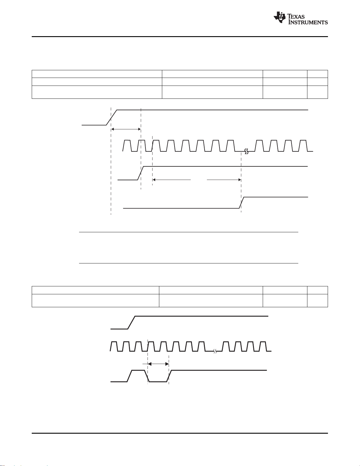
V
CC
XIClock
Hardware
RESET_N
DualFunctionPins
BecomeEnabled AsOutputs
Input
Output
T0338-01
t
1
t
2
V
CC
XIClock
Hardware
RESET_N
T0339-01
t
1
TLK100
SLLS931–AUGUST 2009
7.6 AC Specifications
PARAMETER TEST CONDITIONS MIN TYP MAX UNIT
t
Reset deassertion time from power up 200 μs
1
Time from reset deassertion to the hardware Hardware Configuration Pins are described in
t
2
configuration pins transition to output drivers the Pin Description section.
www.ti.com
Table 7-1. Power Up Timing
46 ns
Figure 7-1. Power Up Timing
NOTE
It is important to choose pull-up and/or pull-down resistors for each of the hardware
configuration pins that provide fast RC time constants in order to latch-in the proper value
prior to the pin transitioning to an output driver.
Table 7-2. Reset Timing
PARAMETER TEST CONDITIONS MIN TYP MAX UNIT
t
RESET pulse width 1 μs
1
XI Clock must be stable for at min. of 1ms
during RESET pulse low time.
58 Electrical Specifications Copyright © 2009, Texas Instruments Incorporated
Figure 7-2. Reset Timing
Submit Documentation Feedback
Product Folder Link(s): TLK100
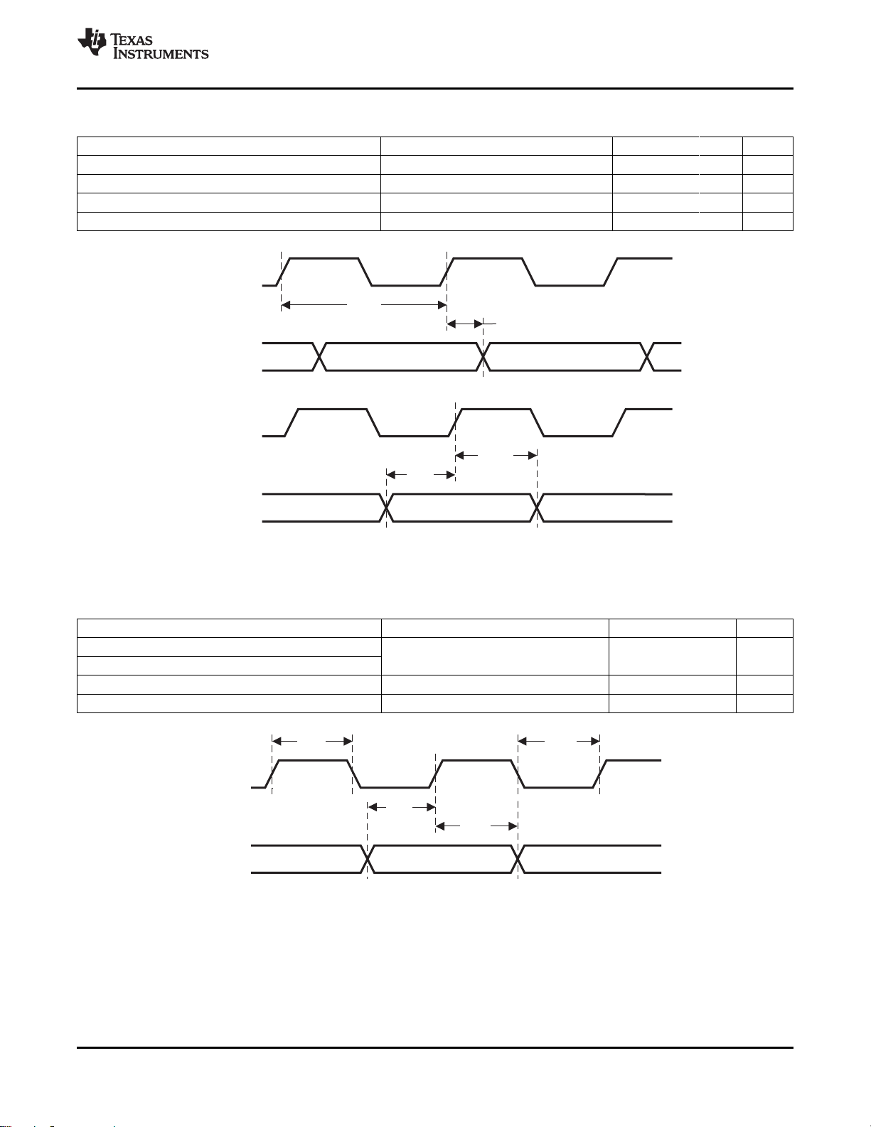
MDC
MDC
MDIO (Output)
MDIO (Input)
Valid Data
T0340-01
t
1
t
2
t
4
t
3
TX_CLK
TXD[3:0]
TX_EN
Valid Data
T0341-01
t
1
t
2
t
4
t
3
TLK100
www.ti.com
t
1
t
2
t
3
t
4
SLLS931–AUGUST 2009
Table 7-3. MII Serial Management Timing
PARAMETER TEST CONDITIONS MIN TYP MAX UNIT
MDC Frequency 2.5 25 MHz
MDC to MDIO (Output) Delay Time 0 ns
MDIO (Input) to MDC Hold Time 10 ns
MDIO (Input) to MDC Setup Time 10 ns
Figure 7-3. MII Serial Management Timing
Table 7-4. 100Mb/s MII Transmit Timing
PARAMETER TEST CONDITIONS MIN TYP MAX UNIT
t
1
t
2
t
3
t
4
TX_CLK High Time
TX_CLK Low Time
100 Mb/s Normal mode 16 20 24 ns
TXD[3:0], TX_EN Data Setup to TX_CLK 100 Mb/s Normal mode 10 ns
TXD[3:0], TX_EN Data Hold from TX_CLK 100 Mb/s Normal mode 0 ns
Figure 7-4. 100Mb/s MII Transmit Timing
Copyright © 2009, Texas Instruments Incorporated Electrical Specifications 59
Submit Documentation Feedback
Product Folder Link(s): TLK100

RX_CLK
Valid Data
RXD[3:0]
RX_DV
RX_ER
T0342-01
t
1
t
2
t
3
TX_CLK
TX_EN
TXD
PMD Output Pair
(J/K)
IDLE
DATA
T0343-01
t
1
TLK100
SLLS931–AUGUST 2009
www.ti.com
Table 7-5. 100Mb/s MII Receive Timing
PARAMETER
t
1
t
2
t
3
RX_CLK High Time
RX_CLK Low Time
RX_CLK to RXD[3:0], RX_DV, RX_ER Delay 100 Mb/s Normal mode 10 30 ns
(1) RX_CLK may be held low or high for a longer period of time during transition between reference and recovered clocks. Minimum high
and low times will not be violated.
(1)
TEST CONDITIONS MIN TYP MAX UNIT
100 Mb/s Normal mode 16 20 24 ns
Figure 7-5. 100Mb/s MII Receive Timing
Table 7-6. 100BASE-TX Transmit Packet Latency Timing
PARAMETER TEST CONDITIONS MIN TYP MAX UNIT
t
1
TX_CLK to PMD Output Pair Latency 100 Mb/s Normal mode
(1) For Normal mode, latency is determined by measuring the time from the first rising edge of TX_CLK occurring after the assertion of
TX_EN to the first bit of the 'J' code group as output from the PMD Output Pair. 1 bit time = 10ns in 100 Mb/s mode.
(1)
8.6 bits
Figure 7-6. 100BASE-TX Transmit Packet Latency Timing
60 Electrical Specifications Copyright © 2009, Texas Instruments Incorporated
Submit Documentation Feedback
Product Folder Link(s): TLK100

TX_CLK
TXD
TX_EN
PMD Output Pair
(T/R)DATA IDLE
(T/R)
DATA
IDLE
T0344-01
t
1
PMD Output Pair
+1 rise
+1fall
–1fall
–1 rise
90%
10%
10%
90%
PMDOutput Pair
EyePattern
T0345-01
t
1
t
1
t
1
t
1
t
2
t
2
TLK100
www.ti.com
t
1
SLLS931–AUGUST 2009
Table 7-7. 100BASE-TX Transmit Packet Deassertion Timing
PARAMETER TEST CONDITIONS MIN TYP MAX UNIT
TX_CLK to PMD Output Pair deassertion 100 Mb/s Normal mode 8.6 bits
Figure 7-7. 100BASE-TX Transmit Packet Latency Timing
Table 7-8. 100BASE-TX Transmit Timing (t
and Jitter)
R/F
PARAMETER TEST CONDITIONS MIN TYP MAX UNIT
t
1
t
2
100 Mb/s PMD Output Pair tRand t
100 Mb/s tRand tFMismatch
100 Mb/s PMD Output Pair Transmit Jitter 1.4 ns
(1)
F
(2)
3 4 5 ns
500 ps
(1) Rise and fall times taken at 10% and 90% of the +1 or -1 amplitude.
(2) Normal Mismatch is the difference between the maximum and minimum of all rise and fall times.
Copyright © 2009, Texas Instruments Incorporated Electrical Specifications 61
Figure 7-8. 100BASE-TX Transmit Timing (t
Submit Documentation Feedback
Product Folder Link(s): TLK100
R/F
and Jitter)
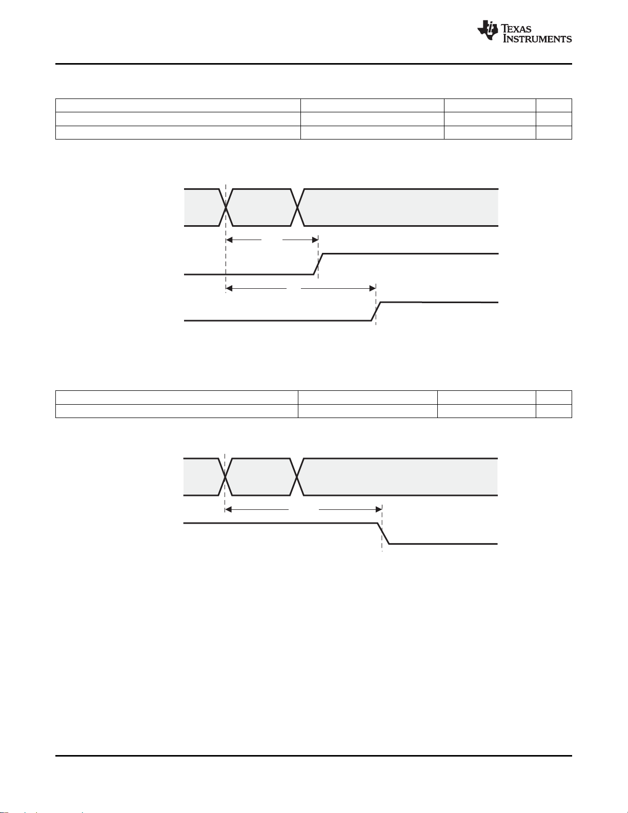
IDLE
(J/K)
Data
t
1
CRS
PMDInputPair
RXD[3:0]
RX_DV
RX_ER
T0346-01
t
2
DATA
(T/R)
IDLE
PMDInputPair
CRS
T0347-01
t
1
TLK100
SLLS931–AUGUST 2009
www.ti.com
Table 7-9. 100BASE-TX Receive Packet Latency Timing
PARAMETER TEST CONDITIONS
t
Carrier Sense ON Delay
1
t
Receive Data Latency 100 Mb/s Normal mode 18.4 bits
2
(2)
100 Mb/s Normal mode 13.6 bits
(1) PMD Input Pair voltage amplitude is greater than the Signal Detect Turn-On Threshold Value.
(2) Carrier Sense On Delay is determined by measuring the time from the first bit of the “J” code group to the assertion of Carrier Sense.
(3) 1 bit time = 10 ns in 100 Mb/s mode
(1)
MIN TYP MAX UNIT
Figure 7-9. 100BASE-TX Receive Packet Latency Timing
(3)
Table 7-10. 100BASE-TX Receive Packet Deassertion Timing
PARAMETER TEST CONDITIONS MIN TYP MAX UNIT
t
1
Carrier Sense OFF Delay
(1)
100 Mb/s Normal mode 13.6 bits
(2)
(1) Carrier Sense Off Delay is determined by measuring the time from the first bit of the “T” code group to the deassertion of Carrier Sense.
(2) 1 bit time = 10 ns in 100 Mb/s mode
Figure 7-10. 100BASE-TX Receive Packet Deassertion Timing
62 Electrical Specifications Copyright © 2009, Texas Instruments Incorporated
Submit Documentation Feedback
Product Folder Link(s): TLK100

TX_CLK
Valid Data
TXD[3:0]
TX_EN
T0348-01
t
2
t
4
t
1
t
3
RX_CLK
Valid Data
RXD[3:0]
RX_DV
T0349-01
t
1
t
2
t
4
t
3
TLK100
www.ti.com
t
1
t
2
t
3
t
4
SLLS931–AUGUST 2009
Table 7-11. 10 Mb/s MII Transmit Timing
PARAMETER TEST CONDITIONS MIN TYP MAX UNIT
TX_CLK Low Time
TX_CLK High Time
10 Mb/s MII mode 190 200 210 ns
TXD[3:0], TX_EN Data Setup to TX_CLK ↓ 10 Mb/s MII mode 25 ns
TXD[3:0], TX_EN Data Hold from TX_CLK ↑ 10 Mb/s MII mode 0 ns
Figure 7-11. 10 Mb/s MII Transmit Timing
Table 7-12. 10Mb/s MII Receive Timing
PARAMETER
t
1
t
2
t
3
t
4
RX_CLK High Time
RX_CLK Low Time
RX_CLK rising edge delay from RXD[3:0], RX_DV Valid 10 Mb/s MII mode 100 ns
RX_CLK to RXD[3:0], RX_DV Delay 10 Mb/s MII mode 100 ns
(1)
TEST CONDITIONS MIN TYP MAX UNIT
160 200 240 ns
(1) RX_CLK may be held low for a longer period of time during transition between reference and recovered clocks. Minimum high and low
times will not be violated.
Figure 7-12. 10Mb/s MII Receive Timing
Copyright © 2009, Texas Instruments Incorporated Electrical Specifications 63
Submit Documentation Feedback
Product Folder Link(s): TLK100
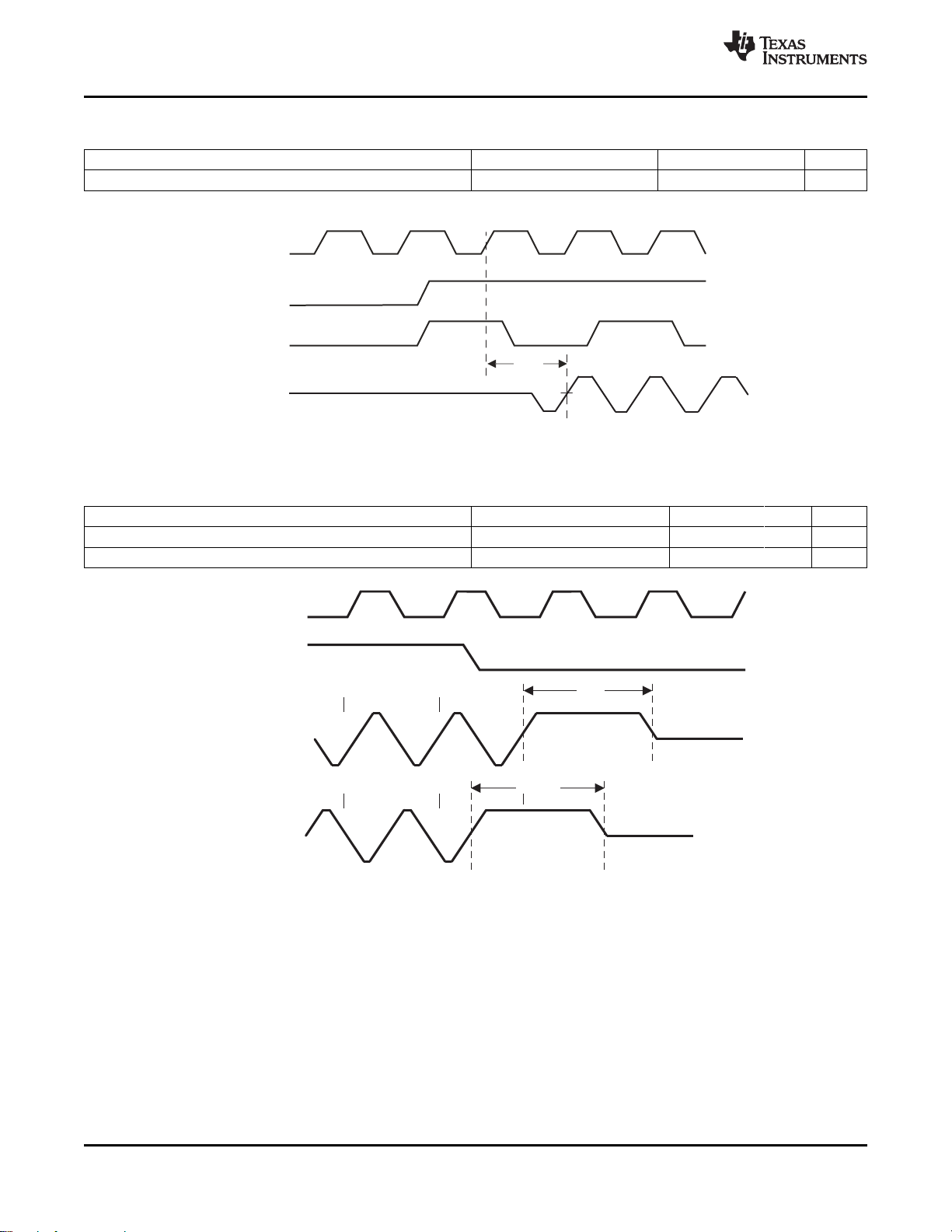
TX_CLK
TX_EN
TXD
PMD Output Pair
t
1
TX_CLK
TX_EN
PMD Output Pair
0 0
1 1
PMD Output Pair
t
1
t
2
TLK100
SLLS931–AUGUST 2009
Table 7-13. 10BASE-T Transmit Timing (Start of Packet)
PARAMETER TEST CONDITIONS MIN TYP MAX UNIT
t
Transmit Output Delay from the Falling Edge of TX_CLK 10 Mb/s MII mode 5.8 bits
1
(1) (1) 1 bit time = 100ns in 10Mb/s.
Figure 7-13. 10BASE-T Transmit Timing (Start of Packet)
Table 7-14. 10BASE-T Transmit Timing (End of Packet)
PARAMETER TEST CONDITIONS MIN TYP MAX UNIT
t
1
t
2
End of Packet High Time (with ‘0’ ending bit) 250 310 ns
End of Packet High Time (with ‘1’ ending bit) 250 310 ns
www.ti.com
(1)
Figure 7-14. 10BASE-T Transmit Timing (End of Packet)
64 Electrical Specifications Copyright © 2009, Texas Instruments Incorporated
Submit Documentation Feedback
Product Folder Link(s): TLK100

1 SFDBitDecoded
st
10 10 10 10 10 11
TPRD
CRS
RX_CLK
RX_DV
RXD[3:0]
0000 Preamble
SFD
Data
T0354-01
t
1
t
2
t
3
1 0 1 IDLE
PMDInputPair
RX_CLK
CRS
t
1
TLK100
www.ti.com
Table 7-15. 10BASE-T Receive Timing (Start of Packet)
PARAMETER TEST CONDITIONS MIN TYP MAX UNIT
t
1
t
2
t
3
(1) 10BASE-T RX_DV Latency is measured from first bit of decoded SFD on the wire to the assertion of RX_DV
Carrier Sense Turn On Delay (PMD Input Pair to MII_CRS) 550 1000 ns
RX_DV Latency
Receive Data Latency 14 bits
(1)
Measurement shown from
SFD
SLLS931–AUGUST 2009
9.3 bits
Figure 7-15. 10BASE-T Receive Timing (Start of Packet)
Table 7-16. 10BASE-T Receive Timing (End of Packet)
PARAMETER TEST CONDITIONS MIN TYP MAX UNIT
t
1
Carrier Sense Turn Off Delay 1.3 μs
Figure 7-16. 10BASE-T Receive Timing (End of Packet)
Copyright © 2009, Texas Instruments Incorporated Electrical Specifications 65
Submit Documentation Feedback
Product Folder Link(s): TLK100
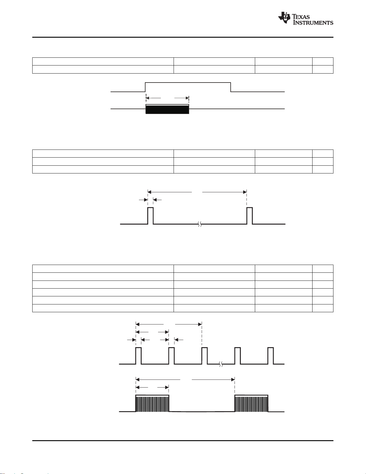
TXE
PMD Output Pair
T0357-01
t
1
NormalLinkPulse(s)
T0358-01
t
1
t
2
FastLinkPulse(s)
Clock
Pulse
Data
Pulse
Clock
Pulse
FLP Burst FLP Burst
T0359-01
t
1
t
2
t
3
t
3
t
4
t
5
TLK100
SLLS931–AUGUST 2009
t
1
t
1
t
2
Jabber Activation Time 100 ms
Pulse Period 16 ms
Pulse Width 100 ns
(1) Transmit timing
www.ti.com
Table 7-17. 10Mb/s Jabber Timing
PARAMETER TEST CONDITIONS MIN TYP MAX UNIT
Figure 7-17. 10Mb/s Jabber Timing
Table 7-18. 10BASE-T Normal Link Pulse Timing
PARAMETER
(1)
TEST CONDITIONS MIN TYP MAX UNIT
Figure 7-18. 10BASE-T Normal Link Pulse Timing
Table 7-19. Auto-Negotiation Fast Link Pulse (FLP) Timing
PARAMETER TEST CONDITIONS MIN TYP MAX UNIT
t
1
t
2
t
3
t
4
t
5
Clock Pulse to Clock Pulse Period 125 μs
Clock Pulse to Data Pulse Period Data = 1 62 μs
Clock, Data Pulse Width 114 ns
FLP Burst to FLP Burst Period 16 ms
Burst Width 2 ms
66 Electrical Specifications Copyright © 2009, Texas Instruments Incorporated
Figure 7-19. Auto-Negotiation Fast Link Pulse (FLP) Timing
Submit Documentation Feedback
Product Folder Link(s): TLK100
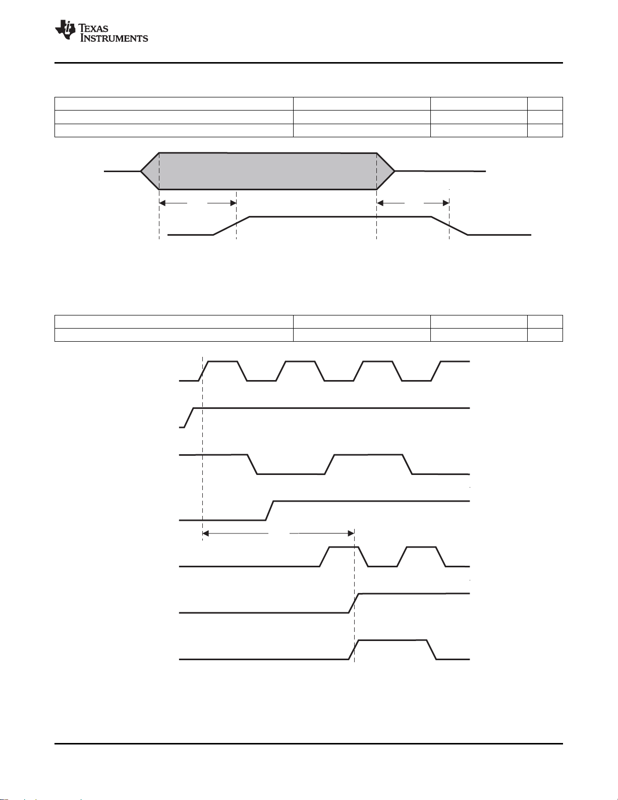
PMDInputPair
SD+Intermal
T0360-01
t
1
t
2
TX_CLK
TX_EN
TXD[3:0]
CRS
RX_CLK
RX_DV
RXD[3:0]
T0361-01
t
1
TLK100
www.ti.com
Table 7-20. 100BASE-TX Signal Detect Timing
PARAMETER TEST CONDITIONS MIN TYP MAX UNIT
t
1
t
2
SD Internal Turn-on Time 100 μs
SD Internal Turn-off Time 500 μs
NOTE: The signal amplitude on PMD Input Pair must be TP-PMD compliant.
Figure 7-20. 100BASE-TX Signal Detect Timing
Table 7-21. 100 Mb/s Internal Loopback Timing
PARAMETER TEST CONDITIONS MIN TYP MAX UNIT
t
1
TX_EN to RX_DV Loopback 100 Mb/s internal loopback mode 272 ns
SLLS931–AUGUST 2009
(1) Due to the nature of the descrambler function, all 100BASE-TX Loopback modes will cause an initial dead-time of up to 550 μs
during which time no data is present at the receive MII outputs. The 100BASE-TX timing specified is based on device delays after
the initial 550µs dead-time.
(2) Measurement is made from the first rising edge of TX_CLK after assertion of TX_EN.
Figure 7-21. 100 Mb/s Internal Loopback Timing
Copyright © 2009, Texas Instruments Incorporated Electrical Specifications 67
Submit Documentation Feedback
Product Folder Link(s): TLK100

TX_CLK
TX_EN
TXD[3:0]
CRS
RX_CLK
RX_DV
RXD[3:0]
T0362-01
t
1
ISOLATE NORMAL
MODE
H/WorS/WReset
T0365-01
t
1
TLK100
SLLS931–AUGUST 2009
t
1
TX_EN to RX_DV Loopback 10 Mb/s internal loopback mode 2.4 μs
www.ti.com
Table 7-22. 10 Mb/s Internal Loopback Timing
PARAMETER TEST CONDITIONS MIN TYP MAX UNIT
NOTE: Measurement is made from the first rising edge of TX_CLK after assertion of TX_EN.
Figure 7-22. 10 Mb/s Internal Loopback Timing
Table 7-23. Isolation Timing
PARAMETER TEST CONDITIONS MIN TYP MAX UNIT
t
1
68 Electrical Specifications Copyright © 2009, Texas Instruments Incorporated
From Deassertion of S/W or H/W Reset to transition from Isolate to Normal
mode
Figure 7-23. Isolation Timing
Submit Documentation Feedback
Product Folder Link(s): TLK100
65 ns

XI
25MHz_OUT
T0366-01
t
1
t
2
t
3
RX_CLK
Valid Data
RXD[3:0]
RX_DV
RX_ER
t
1
TLK100
www.ti.com
Table 7-24. 25 MHz_OUT Timing
PARAMETER TEST CONDITIONS MIN TYP MAX UNIT
t
1
t
2
t
3
25 MHz_OUT
25 MHz_OUT
25 MHz_OUT
(1)
propagation delay Relative to XI 8.8 ns
(1)
High Time 20
(1)
Low Time 20
MII mode ns
(1) 25 MHz_OUT characteristics are dependent upon the XI input characteristics.
Figure 7-24. 25 MHz_OUT Timing
Table 7-25. 100 Mb/s MII Loopback Timing
PARAMETER TEST CONDITIONS MIN TYP MAX UNIT
t
1
RX_CLK to RXD[3:0], RX_DV, RX_ER Delay 100 Mb/s MII Loopback mode 1 ns
SLLS931–AUGUST 2009
Figure 7-25. 100 Mb/s MII Loopback Timing
Copyright © 2009, Texas Instruments Incorporated Electrical Specifications 69
Submit Documentation Feedback
Product Folder Link(s): TLK100
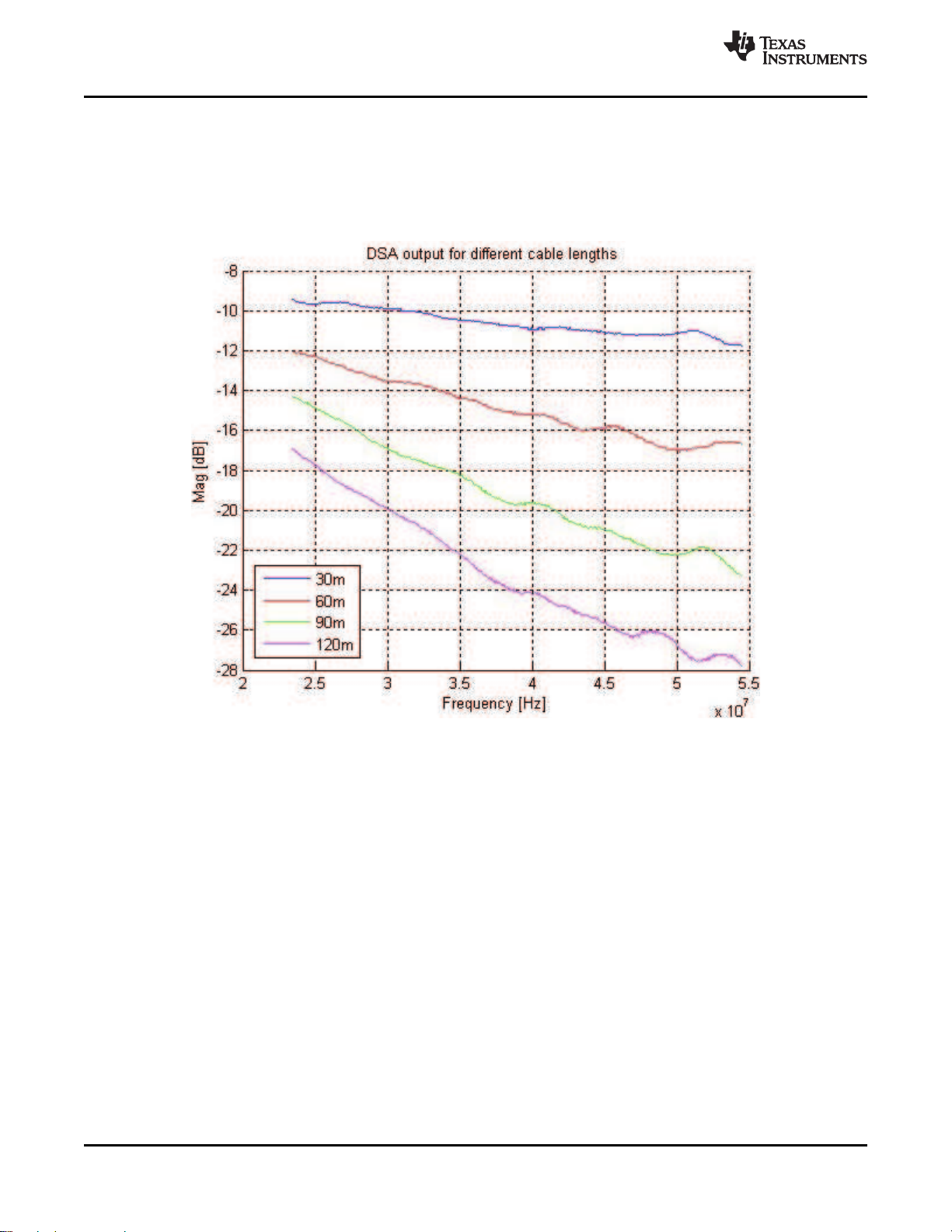
TLK100
SLLS931–AUGUST 2009
8 Appendix A: Digital Spectrum Analyzer (DSA) Output
In the following figure we can see an example to the DSA output. In the figure we can 512 samples of the
spectral analysis of 4 different cable lengths. The first bin is 23.4 MHz. Each following bin represents
61kHz increment. We can see in a very clear way the LPF nature of the channel and how it increases as
we use longer cables.
www.ti.com
70 Appendix A: Digital Spectrum Analyzer (DSA) Output Copyright © 2009, Texas Instruments Incorporated
Submit Documentation Feedback
Product Folder Link(s): TLK100

PACKAGE OPTION ADDENDUM
www.ti.com 1-Sep-2009
PACKAGING INFORMATION
Orderable Device Status
(1)
Package
Type
Package
Drawing
Pins Package
Qty
Eco Plan
TLK100PHP ACTIVE HTQFP PHP 48 250 Green (RoHS &
(2)
Lead/Ball Finish MSL Peak Temp
CU NIPDAU Level-3-260C-168 HR
(3)
no Sb/Br)
TLK100PHPR ACTIVE HTQFP PHP 48 1000 Green (RoHS &
CU NIPDAU Level-3-260C-168 HR
no Sb/Br)
(1)
The marketing status values are defined as follows:
ACTIVE: Product device recommended for new designs.
LIFEBUY: TI has announced that the device will be discontinued, and a lifetime-buy period is in effect.
NRND: Not recommended for new designs. Device is in production to support existing customers, but TI does not recommend using this part in
a new design.
PREVIEW: Device has been announced but is not in production. Samples may or may not be available.
OBSOLETE: TI has discontinued the production of the device.
(2)
Eco Plan - The planned eco-friendly classification: Pb-Free (RoHS), Pb-Free (RoHS Exempt), or Green (RoHS & no Sb/Br) - please check
http://www.ti.com/productcontent for the latest availability information and additional product content details.
TBD: The Pb-Free/Green conversion plan has not been defined.
Pb-Free (RoHS): TI's terms "Lead-Free" or "Pb-Free" mean semiconductor products that are compatible with the current RoHS requirements
for all 6 substances, including the requirement that lead not exceed 0.1% by weight in homogeneous materials. Where designed to be soldered
at high temperatures, TI Pb-Free products are suitable for use in specified lead-free processes.
Pb-Free (RoHS Exempt): This component has a RoHS exemption for either 1) lead-based flip-chip solder bumps used between the die and
package, or 2) lead-based die adhesive used between the die and leadframe. The component is otherwise considered Pb-Free (RoHS
compatible) as defined above.
Green (RoHS & no Sb/Br): TI defines "Green" to mean Pb-Free (RoHS compatible), and free of Bromine (Br) and Antimony (Sb) based flame
retardants (Br or Sb do not exceed 0.1% by weight in homogeneous material)
(3)
MSL, Peak Temp. -- The Moisture Sensitivity Level rating according to the JEDEC industry standard classifications, and peak solder
temperature.
Important Information and Disclaimer:The information provided on this page represents TI's knowledge and belief as of the date that it is
provided. TI bases its knowledge and belief on information provided by third parties, and makes no representation or warranty as to the
accuracy of such information. Efforts are underway to better integrate information from third parties. TI has taken and continues to take
reasonable steps to provide representative and accurate information but may not have conducted destructive testing or chemical analysis on
incoming materials and chemicals. TI and TI suppliers consider certain information to be proprietary, and thus CAS numbers and other limited
information may not be available for release.
In no event shall TI's liability arising out of such information exceed the total purchase price of the TI part(s) at issue in this document sold by TI
to Customer on an annual basis.
Addendum-Page 1


IMPORTANT NOTICE
Texas Instruments Incorporated and its subsidiaries (TI) reserve the right to make corrections, modifications, enhancements, improvements,
and other changes to its products and services at any time and to discontinue any product or service without notice. Customers should
obtain the latest relevant information before placing orders and should verify that such information is current and complete. All products are
sold subject to TI’s terms and conditions of sale supplied at the time of order acknowledgment.
TI warrants performance of its hardware products to the specifications applicable at the time of sale in accordance with TI’s standard
warranty. Testing and other quality control techniques are used to the extent TI deems necessary to support this warranty. Except where
mandated by government requirements, testing of all parameters of each product is not necessarily performed.
TI assumes no liability for applications assistance or customer product design. Customers are responsible for their products and
applications using TI components. To minimize the risks associated with customer products and applications, customers should provide
adequate design and operating safeguards.
TI does not warrant or represent that any license, either express or implied, is granted under any TI patent right, copyright, mask work right,
or other TI intellectual property right relating to any combination, machine, or process in which TI products or services are used. Information
published by TI regarding third-party products or services does not constitute a license from TI to use such products or services or a
warranty or endorsement thereof. Use of such information may require a license from a third party under the patents or other intellectual
property of the third party, or a license from TI under the patents or other intellectual property of TI.
Reproduction of TI information in TI data books or data sheets is permissible only if reproduction is without alteration and is accompanied
by all associated warranties, conditions, limitations, and notices. Reproduction of this information with alteration is an unfair and deceptive
business practice. TI is not responsible or liable for such altered documentation. Information of third parties may be subject to additional
restrictions.
Resale of TI products or services with statements different from or beyond the parameters stated by TI for that product or service voids all
express and any implied warranties for the associated TI product or service and is an unfair and deceptive business practice. TI is not
responsible or liable for any such statements.
TI products are not authorized for use in safety-critical applications (such as life support) where a failure of the TI product would reasonably
be expected to cause severe personal injury or death, unless officers of the parties have executed an agreement specifically governing
such use. Buyers represent that they have all necessary expertise in the safety and regulatory ramifications of their applications, and
acknowledge and agree that they are solely responsible for all legal, regulatory and safety-related requirements concerning their products
and any use of TI products in such safety-critical applications, notwithstanding any applications-related information or support that may be
provided by TI. Further, Buyers must fully indemnify TI and its representatives against any damages arising out of the use of TI products in
such safety-critical applications.
TI products are neither designed nor intended for use in military/aerospace applications or environments unless the TI products are
specifically designated by TI as military-grade or "enhanced plastic." Only products designated by TI as military-grade meet military
specifications. Buyers acknowledge and agree that any such use of TI products which TI has not designated as military-grade is solely at
the Buyer's risk, and that they are solely responsible for compliance with all legal and regulatory requirements in connection with such use.
TI products are neither designed nor intended for use in automotive applications or environments unless the specific TI products are
designated by TI as compliant with ISO/TS 16949 requirements. Buyers acknowledge and agree that, if they use any non-designated
products in automotive applications, TI will not be responsible for any failure to meet such requirements.
Following are URLs where you can obtain information on other Texas Instruments products and application solutions:
Products Applications
Amplifiers amplifier.ti.com Audio www.ti.com/audio
Data Converters dataconverter.ti.com Automotive www.ti.com/automotive
DLP® Products www.dlp.com Broadband www.ti.com/broadband
DSP dsp.ti.com Digital Control www.ti.com/digitalcontrol
Clocks and Timers www.ti.com/clocks Medical www.ti.com/medical
Interface interface.ti.com Military www.ti.com/military
Logic logic.ti.com Optical Networking www.ti.com/opticalnetwork
Power Mgmt power.ti.com Security www.ti.com/security
Microcontrollers microcontroller.ti.com Telephony www.ti.com/telephony
RFID www.ti-rfid.com Video & Imaging www.ti.com/video
RF/IF and ZigBee® Solutions www.ti.com/lprf Wireless www.ti.com/wireless
Mailing Address: Texas Instruments, Post Office Box 655303, Dallas, Texas 75265
Copyright © 2009, Texas Instruments Incorporated
 Loading...