

Page 1
TLE202x, TLE202xA, TLE202xB, TLE202xY
EXCALIBUR HIGH-SPEED LOW-POWER PRECISION
OPERATIONAL AMPLIFIERS
SLOS191B – FEBRUARY 1997 – REVISED JANUARY 2002
D
Supply Current . . . 300 µA Max
D
High Unity-Gain Bandwidth ...2 MHz Typ
D
High Slew Rate . . . 0.45 V/µs Min
D
Supply-Current Change Over Military Temp
Range ...10 µA Typ at V
D
Specified for Both 5-V Single-Supply and
CC ±
= ± 15 V
±15-V Operation
D
Phase-Reversal Protection
description
The TLE202x, TLE202xA, and TLE202xB devices are precision, high-speed, low-power operational amplifiers
using a new Texas Instruments Excalibur process. These devices combine the best features of the OP21 with
highly improved slew rate and unity-gain bandwidth.
The complementary bipolar Excalibur process utilizes isolated vertical pnp transistors that yield dramatic
improvement in unity-gain bandwidth and slew rate over similar devices.
The addition of a bias circuit in conjunction with this process results in extremely stable parameters with both
time and temperature. This means that a precision device remains a precision device even with changes in
temperature and over years of use.
D
High Open-Loop Gain . . . 6.5 V/µV
(136 dB) Typ
D
Low Offset Voltage . . . 100 µV Max
D
Offset Voltage Drift With Time
0.005 µV/mo Typ
D
Low Input Bias Current . . . 50 nA Max
D
Low Noise Voltage . . . 19 nV/√Hz Typ
This combination of excellent dc performance with a common-mode input voltage range that includes the
negative rail makes these devices the ideal choice for low-level signal conditioning applications in either
single-supply or split-supply configurations. In addition, these devices offer phase-reversal protection circuitry
that eliminates an unexpected change in output states when one of the inputs goes below the negative supply
rail.
A variety of available options includes small-outline and chip-carrier versions for high-density systems
applications.
The C-suffix devices are characterized for operation from 0°C to 70°C. The I-suffix devices are characterized
for operation from – 40°C to 85°C. The M-suffix devices are characterized for operation over the full military
temperature range of –55°C to 125°C.
Please be aware that an important notice concerning availability, standard warranty, and use in critical applications of
Texas Instruments semiconductor products and disclaimers thereto appears at the end of this data sheet.
PRODUCTION DATA information is current as of publication date.
Products conform to specifications per the terms of Texas Instruments
standard warranty. Production processing does not necessarily include
testing of all parameters.
POST OFFICE BOX 655303 • DALLAS, TEXAS 75265
Copyright 2002, Texas Instruments Incorporated
1
Page 2
TLE202x, TLE202xA, TLE202xB, TLE202xY
CHIP
TLE2021CDBLE
t
µ
TLE2021AIP
µ
CHIP
t
300 µV
TLE2022ACD
TLE2022ACP
t
300 µV
TLE2022AID
TLE2022AIP
55 C
150 µV
TLE2022BMJG
CHIP
500 µV
TLE2024BCDW
TLE2024BCN
µ
500 µV
TLE2024BIDW
TLE2024BIN
µ
µ
EXCALIBUR HIGH-SPEED LOW-POWER PRECISION
OPERATIONAL AMPLIFIERS
SLOS191B – FEBRUARY 1997 – REVISED JANUARY 2002
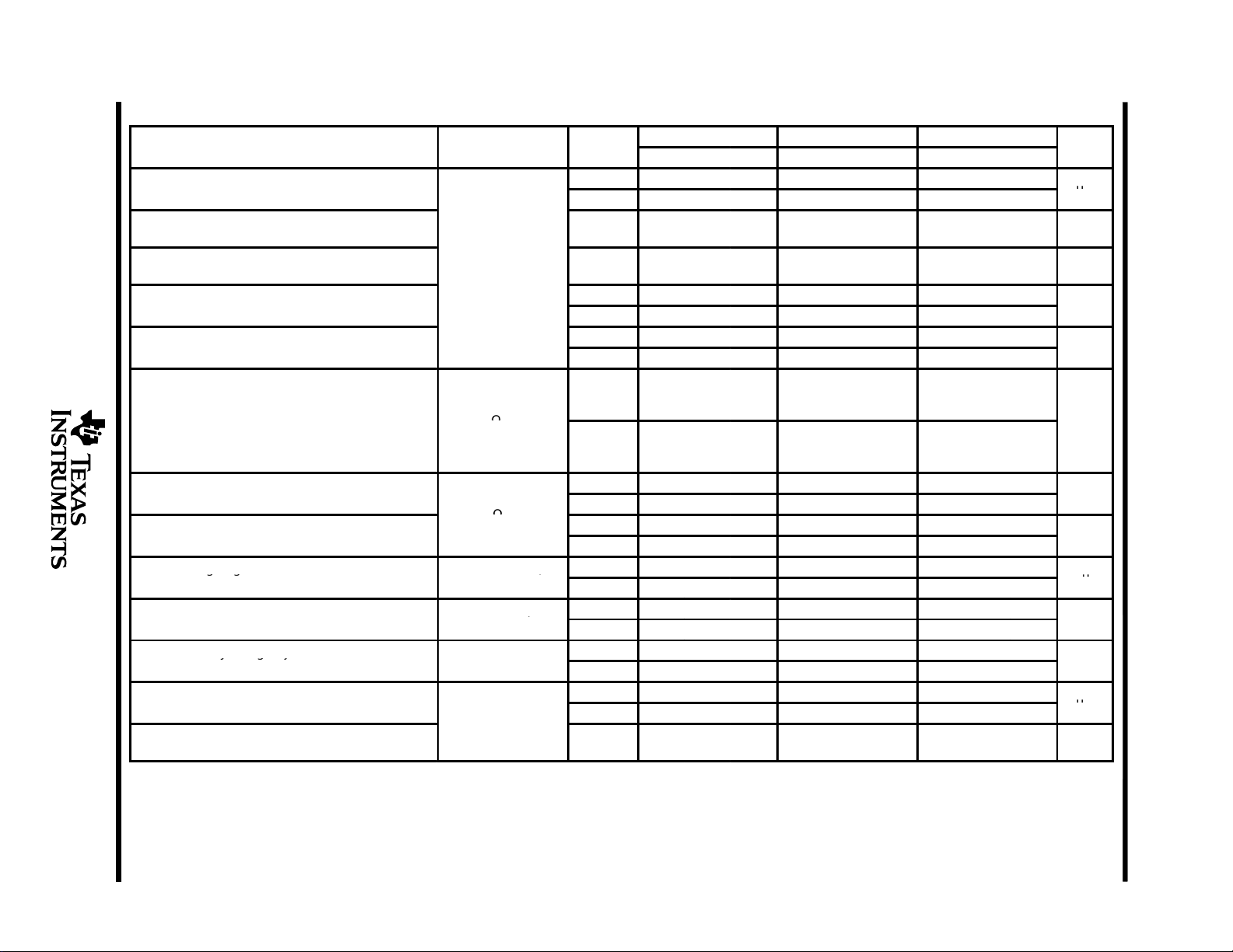
TLE2021 AVAILABLE OPTIONS
PACKAGED DEVICES
VIOmax
T
A
AT 25°C
0°C to 200 µV TLE2021ACD
70°Cµ500 µV TLE2021CD
–40°C
85°C
–55°C 100 µV — TLE2021BMFK TLE2021BMJG —
125°C 500 µV TLE2021MD TLE2021MFK TLE2021MJG TLE2021MP
†
The D packages are available taped and reeled. To order a taped and reeled part, add the suffix R (e.g., TLE2021CDR).
‡
The DB and PW packages are only available left-end taped and reeled.
§
Chip forms are tested at 25°C only.
70°C
–40°C
85°C
–55°C 150 µV — — TLE2022BMJG —
125°Cµ500 µV TLE2022MD TLE2022MFK TLE2022MJG TLE2022MP
†
The D packages are available taped and reeled. To order a taped and reeled part, add the suffix R (e.g., TLE2022CDR).
‡
The DB and PW packages are only available left-end taped and reeled.
§
Chip forms are tested at 25°C only.
200 µV TLE2021AID
o
500 µV TLE2021ID
to
200 µV TLE2021AMD
VIOmax
T
A
AT 25°C
0°C
150 µV
o
500 µV
150 µV
o
500 µV
to
300 µV TLE2022AMD
SMALL
(D)
SMALL
(D)
†
†
OUTLINE
OUTLINE
TLE2022BCD
TLE2022CD
TLE2022BID
TLE2022ID
‡
SSOP
(DB)
— — —
—
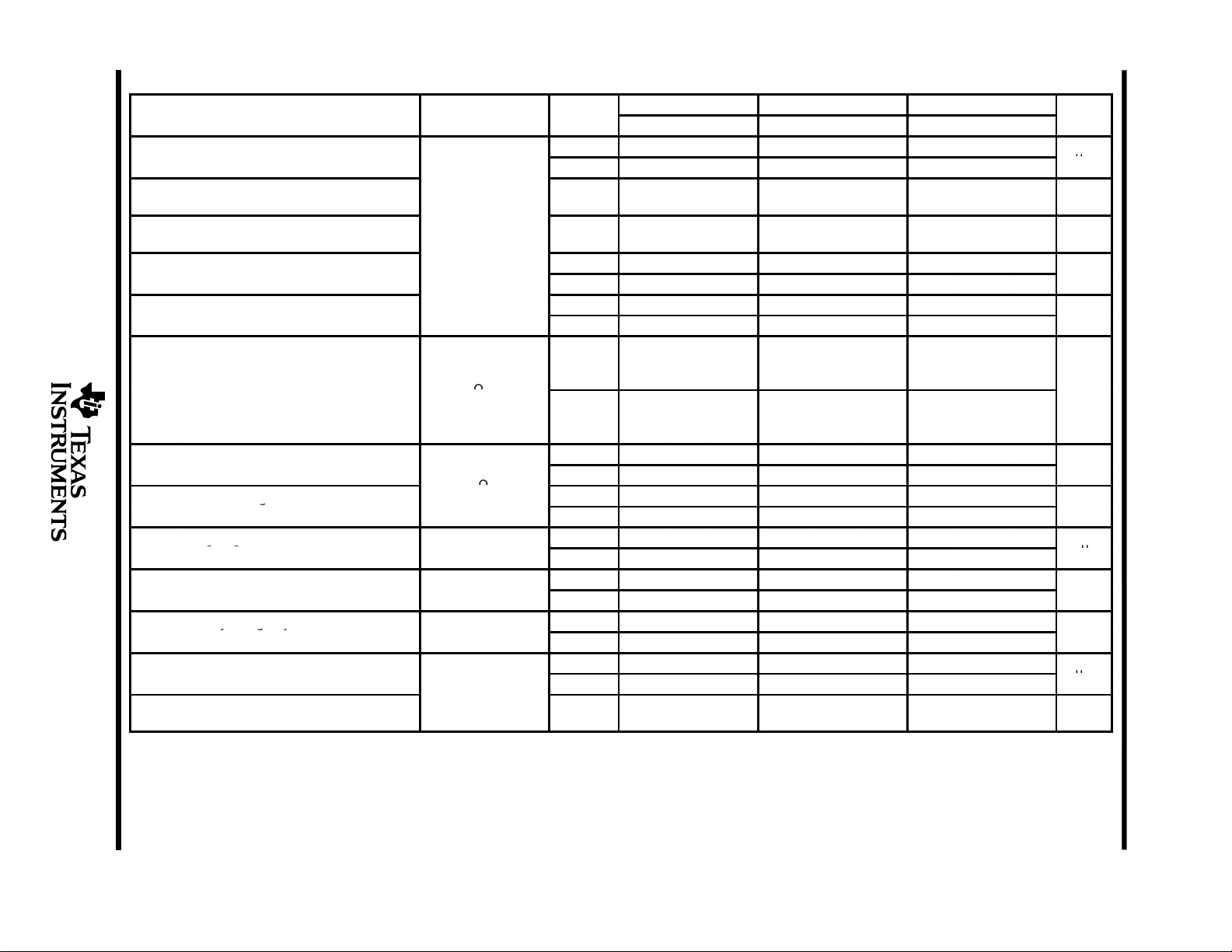
TLE2022 AVAILABLE OPTIONS
‡
SSOP
(DB)
—
—
TLE2022CDBLE
— — —
—
CHIP
CARRIER
(FK)
— —
TLE2021AMFK TLE2021AMJG TLE2021AMP
PACKAGED DEVICES
CHIP
CARRIER
(FK)
— —
TLE2022AMFK
CERAMIC DIP
(JG)
CERAMIC
DIP
(JG)
TLE2022AMJG TLE2022AMP
PLASTIC DIP
(P)
TLE2021ACP
TLE2021CP
TLE2021AIP
TLE2021IP
PLASTIC
DIP
(P)
—
TLE2022CP
—
TLE2022IP
TSSOP
TLE2021CPWLE TLE2021Y
TSSOP
TLE2022CPWLE—TLE2022Y
‡
(PW)
— —
— —
— —
‡
(PW)
—
—
— —
— —
FORM
(Y)
FORM
(Y)
—
§
§
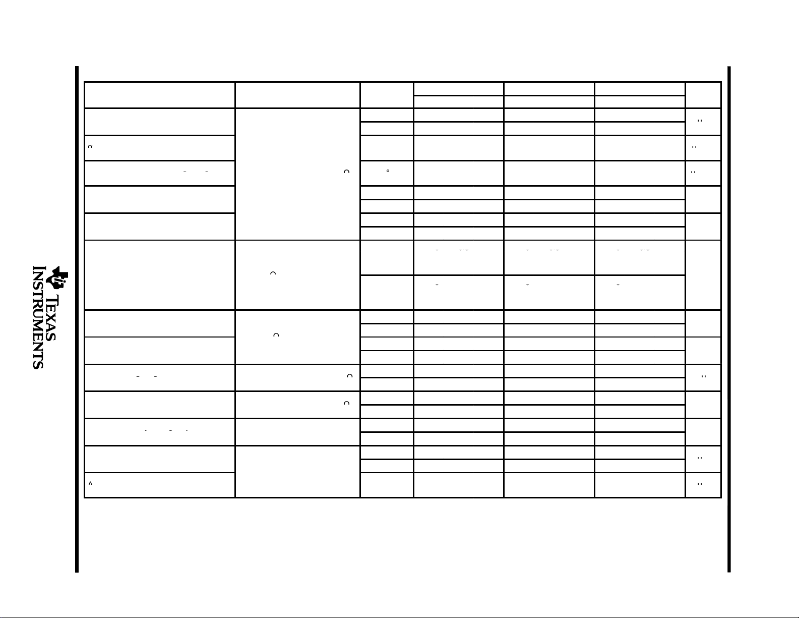
2
T
A
0°C to 70°C
–40°C to 85°C
–55°C to 125°C
§
Chip forms are tested at 25°C only.
VIOmax
AT 25°C
500 µV TLE2024BCDW TLE2024BCN —
750 µV
1000 µV TLE2024CDW TLE2024CN TLE2024Y
500 µV TLE2024BIDW TLE2024BIN
750 µV
1000 µV TLE2024IDW TLE2024IN
500 µV TLE2024BMDW TLE2024BMFK TLE2024BMJ TLE2024BMN
750 µV TLE2024AMDW TLE2024AMFK TLE2024AMJ TLE2024AMN
1000 µV TLE2024MDW TLE2024MFK TLE2024MJ TLE2024MN
TLE2024 AVAILABLE OPTIONS
PACKAGED DEVICES
SMALL
OUTLINE
(DW)
TLE2024ACDW
TLE2024AIDW
POST OFFICE BOX 655303 • DALLAS, TEXAS 75265
CHIP
CARRIER
(FK)
— —
— —
CERAMIC
DIP
(J)
PLASTIC
DIP
(N)
TLE2024ACN —
TLE2024AIN
FORM
(Y)
§
—
—
Page 3
TLE202x, TLE202xA, TLE202xB, TLE202xY
EXCALIBUR HIGH-SPEED LOW-POWER PRECISION
OPERATIONAL AMPLIFIERS
SLOS191B – FEBRUARY 1997 – REVISED JANUARY 2002
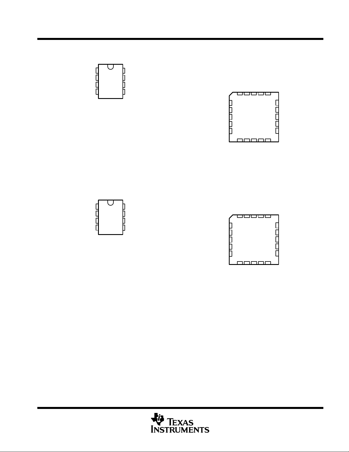
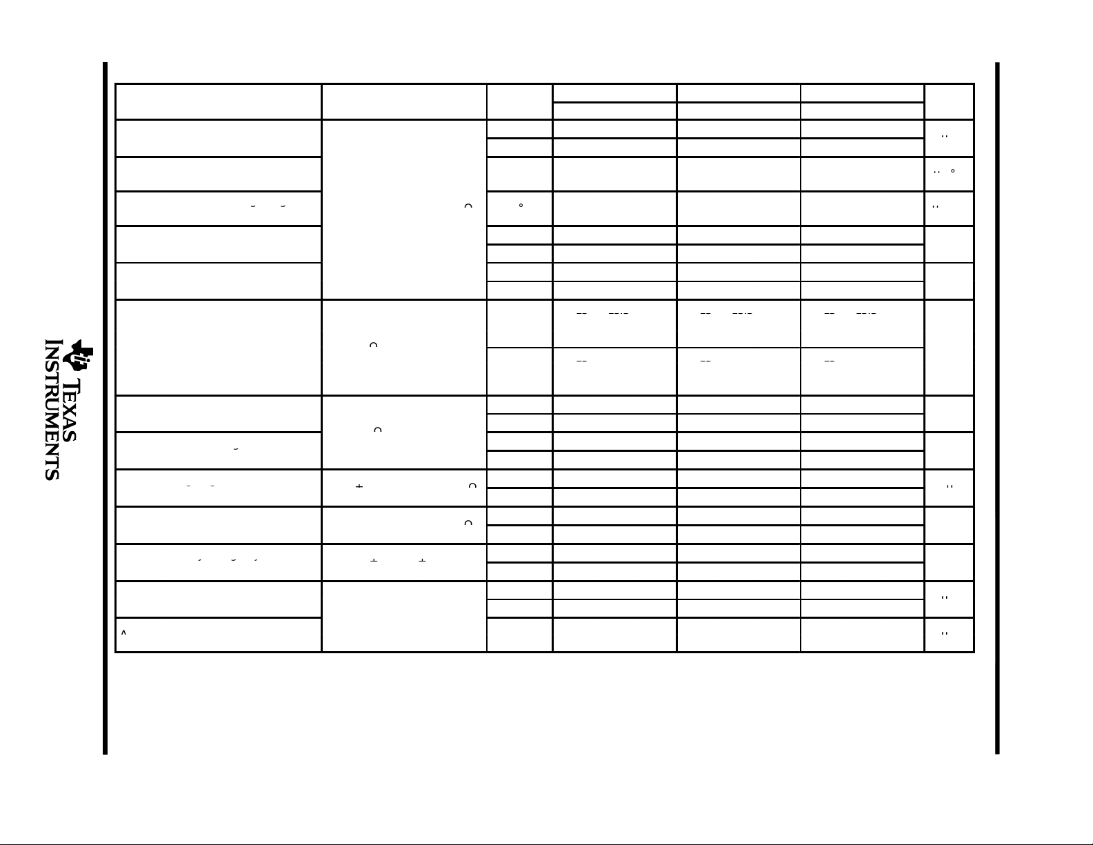
TLE2021
D, DB, JG, P, OR PW PACKAGE
(TOP VIEW)
OFFSET N1
V
/GND
CC –
NC – No internal connection
D, DB, JG, P, OR PW PACKAGE
1OUT
1IN–
1IN+
V
/GND
CC –
IN–
IN+
1
2
3
4
(TOP VIEW)
1
2
3
4
NC
8
V
7
CC+
OUT
6
OFFSET N2
5
V
8
CC+
2OUT
7
2IN–
6
2IN+
5
NC
IN–
NC
IN+
NC
NC
1IN –
NC
1IN +
NC
TLE2021
FK PACKAGE
(TOP VIEW)
NC
OFFSET N1
NCNCNC
NC
3212019
4
5
6
7
8
910111213
NC
NC
GND
CC–
V/
OFFSET N2
FK PACKAGE
(TOP VIEW)
NC
1OUT
NCNCNC
3212019
4
5
6
7
8
910111213
NC
18
V
17
CC+
NC
16
OUT
15
14
NC
CC+
V
NC
18
2OUT
17
NC
16
2IN –
15
14
NC
NC – No internal connection
POST OFFICE BOX 655303 • DALLAS, TEXAS 75265
NC
GND
CC–
V/
NC
2IN +
3
Page 4
TLE202x, TLE202xA, TLE202xB, TLE202xY
EXCALIBUR HIGH-SPEED LOW-POWER PRECISION
OPERATIONAL AMPLIFIERS
SLOS191B – FEBRUARY 1997 – REVISED JANUARY 2002
1OUT
1IN–
1IN+
V
CC+
2IN+
2IN–
2OUT
NC
DW PACKAGE
(TOP VIEW)
16
1
15
2
14
3
13
4
12
5
11
6
10
7
8
9
4OUT
4IN–
4IN+
V
CC –
3IN+
3IN–
3OUT
NC
/GND
1IN+
NC
V
CC+
NC
2IN+
FK PACKAGE
(TOP VIEW)
1IN –
1OUT
NC
3 2 1 20 19
4
5
6
7
8
910111213
4OUT
4IN –
18
17
16
15
14
4IN+
NC
V
CC–
NC
3IN+
/GND
J OR N PACKAGE
(TOP VIEW)
1OUT
V
2OUT
1IN–
1IN+
CC+
2IN+
2IN–
1
2
3
4
5
6
7
14
13
12
11
10
4OUT
4IN–
4IN+
V
CC–
3IN+
3IN–
9
3OUT
8
NC
NC – No internal connection
2IN –
2OUT
3IN –
3OUT
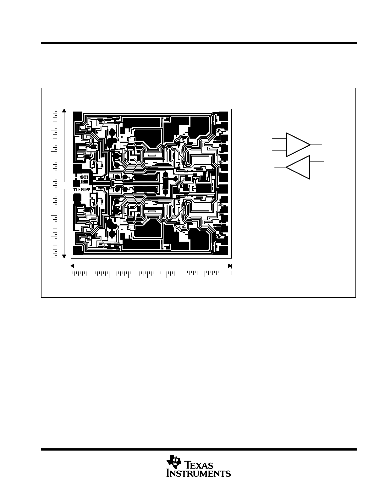
TLE2021Y chip information
This chip, when properly assembled, display characteristics similar to the TLE2021. Thermal compression or
ultrasonic bonding may be used on the doped-aluminum bonding pads. This chip may be mounted with
conductive epoxy or a gold-silicon preform.
BONDING PAD ASSIGNMENTS
(5)(6)(7)
V
V
+
–
CC–
CC+
(7)
(6)
(4)
/GND
OFFSET N1
IN+
IN–
OFFSET N2
(1)
(3)
(2)
(5)
/GND
OUT
78
CHIP THICKNESS: 15 MILS TYPICAL
BONDING PADS: 4 × 4 MILS MINIMUM
T
= 150°C
Jmax
TOLERANCES ARE ±10%.
(1)
(2) (3)
54
4
POST OFFICE BOX 655303 • DALLAS, TEXAS 75265
(4)
ALL DIMENSIONS ARE IN MILS.
PIN (4) IS INTERNALLY CONNECTED
TO BACKSIDE OF CHIP.
Page 5
TLE202x, TLE202xA, TLE202xB, TLE202xY
EXCALIBUR HIGH-SPEED LOW-POWER PRECISION
OPERATIONAL AMPLIFIERS
SLOS191B – FEBRUARY 1997 – REVISED JANUARY 2002
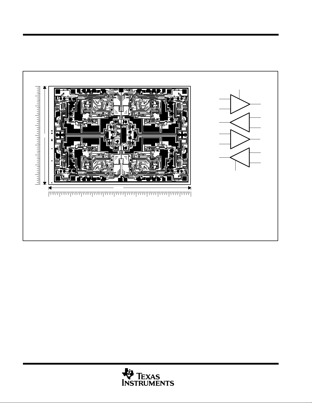
TLE2022Y chip information
This chip, when properly assembled, displays characteristics similar to TLE2022. Thermal compression or
ultrasonic bonding may be used on the doped-aluminum bonding pads. This chip may be mounted with
conductive epoxy or a gold-silicon preform.
BONDING PAD ASSIGNMENTS
80
(8)
(2)
(1)
86
(6)(7)
(5)
(4)
(3)
V
CC+
IN+
IN–
OUT
CHIP THICKNESS: 15 MILS TYPICAL
BONDING PADS: 4 × 4 MILS MINIMUM
TJmax = 150°C
TOLERANCES ARE ±10%.
ALL DIMENSIONS ARE IN MILS.
PIN (4) IS INTERNALLY CONNECTED
TO BACKSIDE OF CHIP.
(3)
(2)
(7)
(8)
+
–
V
CC–
(4)
(1)
OUT
(5)
+
–
(6)
IN+
IN–
POST OFFICE BOX 655303 • DALLAS, TEXAS 75265
5
Page 6
TLE202x, TLE202xA, TLE202xB, TLE202xY
EXCALIBUR HIGH-SPEED LOW-POWER PRECISION
OPERATIONAL AMPLIFIERS
SLOS191B – FEBRUARY 1997 – REVISED JANUARY 2002
TLE2024Y chip information
This chip, when properly assembled, displays characteristics similar to the TLE2024. Thermal compression or
ultrasonic bonding may be used on the doped aluminum-bonding pads. This chip may be mounted with
conductive epoxy or a gold-silicon preform.
BONDING PAD ASSIGNMENTS
V
CC+
(4)
+
–
+
–
+
–
+
–
(11)
CC–/GND
100
1IN+
1IN–
2OUT
2IN+
3IN–
4OUT
(3)
(2)
(7)
(10)
(9)
(14)
V
(1)
(5)
(6)
(8)
(12)
(13)
1OUT
2IN+
2IN–
3OUT
4IN+
4IN–
140
CHIP THICKNESS: 15 MILS TYPICAL
BONDING PADS: 4 × 4 MILS MINIMUM
TJmax = 150°C
TOLERANCES ARE ±10%.
ALL DIMENSIONS ARE IN MILS.
PIN (11) IS INTERNALLY CONNECTED
TO BACKSIDE OF CHIP.
6
POST OFFICE BOX 655303 • DALLAS, TEXAS 75265
Page 7
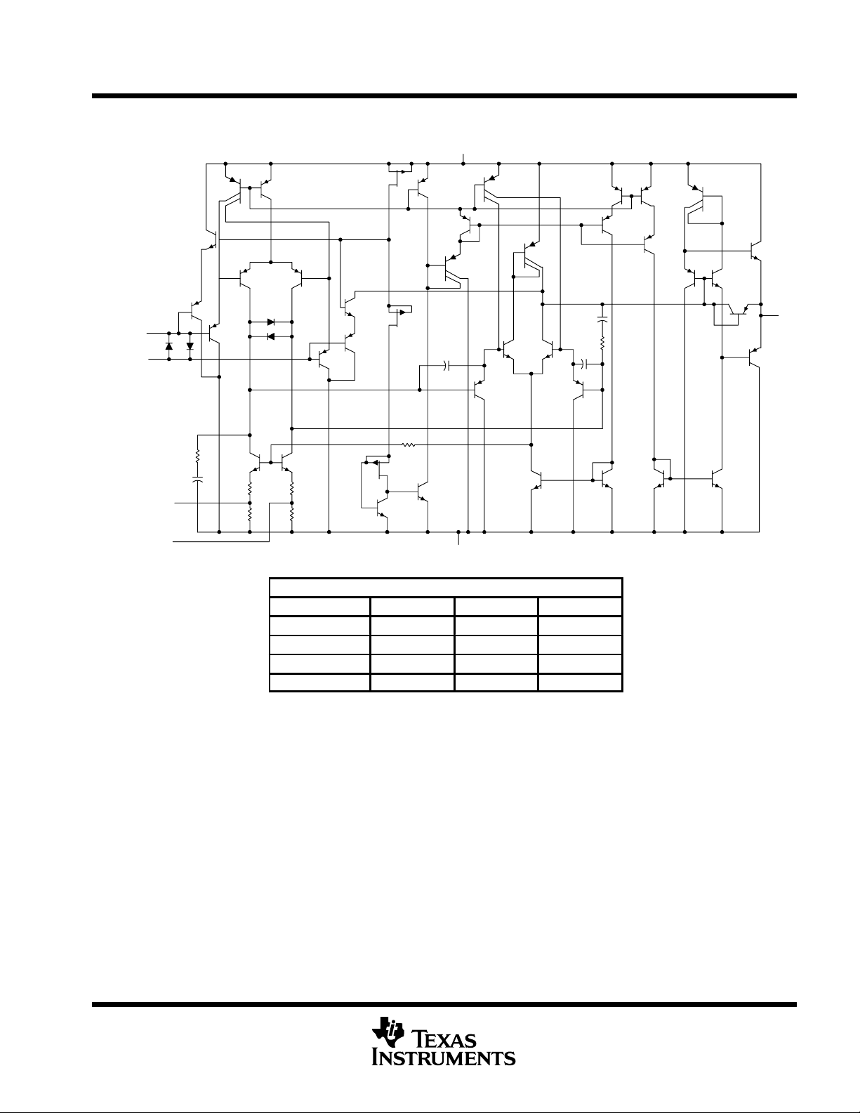
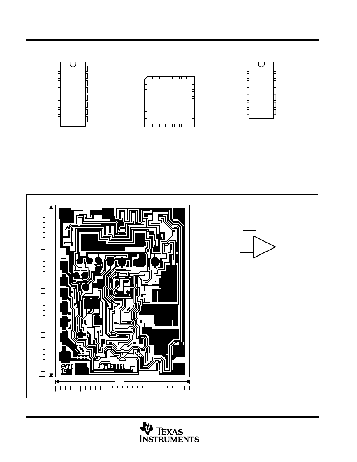
equivalent schematic (each amplifier)
TLE202x, TLE202xA, TLE202xB, TLE202xY
EXCALIBUR HIGH-SPEED LOW-POWER PRECISION
OPERATIONAL AMPLIFIERS
SLOS191B – FEBRUARY 1997 – REVISED JANUARY 2002
V
CC+
IN –
IN +
OFFSET N1
(see Note A)
OFFSET N2
(see Note A)
D1
R1
C1
D2
Q1
Q2
Q3
Q4
R2
R3
Q6
Q5
D3
D4
Q7
Q8
Q9
R4
R5
Q10
Q11
Q12
Q13
Q14
Q15
Q16
R6
Q17
Q18
V
Q19
C2
CC–
Q20
/GND
Q22
Q21
Q24
Q23 Q25
Q26
Q27
C4
R7
C3
Q28
Q29
Q30
Q31
Q33
Q32
Q35
Q34
Q39
Q36
Q38
OUT
Q40
Q37
ACTUAL DEVICE COMPONENT COUNT
COMPONENT TLE2021 TLE2022 TLE2024
Transistors 40 80 160
Resistors 7 14 28
Diodes 4 8 16
Capacitors 4 8 16
POST OFFICE BOX 655303 • DALLAS, TEXAS 75265
7
Page 8
TLE202x, TLE202xA, TLE202xB, TLE202xY
UNIT
Common-mode input voltage, V
V
EXCALIBUR HIGH-SPEED LOW-POWER PRECISION
OPERATIONAL AMPLIFIERS
SLOS191B – FEBRUARY 1997 – REVISED JANUARY 2002
absolute maximum ratings over operating free-air temperature range (unless otherwise noted)
Supply voltage, V
Supply voltage, V
Differential input voltage, V
Input voltage range, V
Input current, I
I
Output current, I
Total current into V
Total current out of V
Duration of short-circuit current at (or below) 25°C (see Note 3) unlimited. . . . . . . . . . . . . . . . . . . . . . . . . . . . . .
Continuous total power dissipation See Dissipation Rating Table. . . . . . . . . . . . . . . . . . . . . . . . . . . . . . . . . . . . .
Operating free-air temperature range, T
Storage temperature range, T
Case temperature for 60 seconds, T
Lead temperature 1,6 mm (1/16 inch) from case for 10 seconds: D, DP, P, or PW package 260°C. . . . . . . .
Lead temperature 1,6 mm (1/16 inch) from case for 60 seconds: JG package 300°C. . . . . . . . . . . . . . . . . . . .
†
Stresses beyond those listed under “absolute maximum ratings” may cause permanent damage to the device. These are stress ratings only, and
functional operation of the device at these or any other conditions beyond those indicated under “recommended operating conditions” is not
implied. Exposure to absolute-maximum-rated conditions for extended periods may affect device reliability.
NOTES: 1. All voltage values, except differential voltages, are with respect to the midpoint between V
2. Dif ferential voltages are at IN+ with respect to IN–. Excessive current flows if a differential input voltage in excess of approximately
±600 mV is applied between the inputs unless some limiting resistance is used.
3. The output may be shorted to either supply. Temperature and/or supply voltages must be limited to ensure that the maximum
dissipation rating is not exceeded.
(see Note 1) 20 V. . . . . . . . . . . . . . . . . . . . . . . . . . . . . . . . . . . . . . . . . . . . . . . . . . . . . . . . . . .
CC+
(see Note 1) –20 V. . . . . . . . . . . . . . . . . . . . . . . . . . . . . . . . . . . . . . . . . . . . . . . . . . . . . . . . . .
CC–
I
(see Note 2) ±0.6 V. . . . . . . . . . . . . . . . . . . . . . . . . . . . . . . . . . . . . . . . . . . . . . . . . .
ID
(any input, see Note 1) ±V
. . . . . . . . . . . . . . . . . . . . . . . . . . . . . . . . . . . . . . . . . . . . . . . .
(each input) ±1 mA. . . . . . . . . . . . . . . . . . . . . . . . . . . . . . . . . . . . . . . . . . . . . . . . . . . . . . . . . . . . . . .
(each output): TLE2021 ±20 mA. . . . . . . . . . . . . . . . . . . . . . . . . . . . . . . . . . . . . . . . . . . . . . . . .
O
TLE2022 ±30 mA. . . . . . . . . . . . . . . . . . . . . . . . . . . . . . . . . . . . . . . . . . . . . . . . .
TLE2024 ±40 mA. . . . . . . . . . . . . . . . . . . . . . . . . . . . . . . . . . . . . . . . . . . . . . . . .
80 mA. . . . . . . . . . . . . . . . . . . . . . . . . . . . . . . . . . . . . . . . . . . . . . . . . . . . . . . . . . . . . . . . . . .
CC+
80 mA. . . . . . . . . . . . . . . . . . . . . . . . . . . . . . . . . . . . . . . . . . . . . . . . . . . . . . . . . . . . . . . . .
CC–
: C suffix 0°C to 70°C. . . . . . . . . . . . . . . . . . . . . . . . . . . . . . . . . . . . . . .
A
I suffix –40°C to 85°C. . . . . . . . . . . . . . . . . . . . . . . . . . . . . . . . . . . . . .
M suffix –55°C to 125°C. . . . . . . . . . . . . . . . . . . . . . . . . . . . . . . . . . . .
–65°C to 150°C. . . . . . . . . . . . . . . . . . . . . . . . . . . . . . . . . . . . . . . . . . . . . . . . . . .
stg
: FK package 260°C. . . . . . . . . . . . . . . . . . . . . . . . . . . . . . . . . . . . . . . . . .
C
CC+
, and V
CC–
.
†
CC
PACKAGE
D–8 725 mW 5.8 mW/°C 464 mW 377 mW 145 mW
DB–8 525 mW 4.2 mW/°C 336 mW ——
DW–16 1025 mW 8.2 mW/°C 656 mW 533 mW 205 mW
FK 1375 mW 11.0 mW/°C 880 mW 715 mW 275 mW
J–14 1375 mW 11.0 mW/°C 880 mW 715 mW 275 mW
JG–8 1050 mW 8.4 mW/°C 672 mW 546 mW 210 mW
N–14 1150 mW 9.2 mW/°C 736 mW 598 mW 230 mW
P–8 1000 mW 8.0 mW/°C 640 mW 520 mW 200 mW
PW–8 525 mW 4.2 mW/°C 336 mW — —
TA ≤ 25°C
POWER RATING
DERATING FACTOR
recommended operating conditions
Supply voltage, V
Operating free-air temperature, T
CC
p
VCC = ± 5 V 0 3.5 0 3.2 0 3.2
IC
V
= ±15 V –15 13.5 –15 13.2 –15 13.2
CC±
A
DISSIPATION RATING TABLE
ABOVE TA = 25°C
POWER RATING
TA = 70°C
C SUFFIX I SUFFIX M SUFFIX
MIN MAX MIN MAX MIN MAX
±2 ±20 ±2 ±20 ±2 ±20 V
0 70 –40 85 –55 125 °C
TA = 85°C
POWER RATING
TA = 125°C
POWER RATING
8
POST OFFICE BOX 655303 • DALLAS, TEXAS 75265
Page 9
POST OFFICE BOX 655303 DALLAS, TEXAS 75265
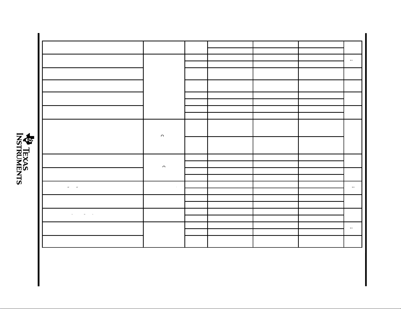
PARAMETER
TEST CONDITIONS
T
†
UNIT
VIOInput offset voltage
V
IC
,
S
IIOInput offset current
nA
IIBInput bias current
nA
V
Common-mode input voltage range
R
50 Ω
V
VOHHigh-level output voltage
V
R
10 kΩ
VOLLow-level output voltage
V
A
gg
O
,
V/µV
CMRR
Common-mode rejection ratio
IC ICR
,
dB
k
ygj
V
5 V to 30 V
dB
ICCSupply current
A
V
O
load
• 9
TLE2021 electrical characteristics at specified free-air temperature, VCC = 5 V (unless otherwise noted)
A
p
α
SVR
∆I
†
Full range is 0°C to 70°C.
NOTE 4: Typical values are based on the input of fset voltage shift observed through 168 hours of operating life test at TA = 150°C extrapolated to TA = 25°C using the Arrhenius equation
Temperature coefficient of
VIO
input offset voltage
Input offset voltage long-term drift
(see Note 4)
p
p
ICR
Large-signal differential V
VD
voltage amplification
Supply-voltage rejection ratio
(∆VCC/∆VIO)
pp
Supply-current change over
CC
operating temperature range
and assuming an activation energy of 0.96 eV.
p
p
p
V
= 0, R
=
S
=
L
= 1.4 V to 4 V,
RL = 10 kΩ
V
= V
RS = 50 Ω
=
CC
= 2.5 V, No
= 50 Ω
min,
25°C 120 600 100 300 80 200
Full range 850 600 300
Full range 2 2 2 µV/°C
25°C 0.005 0.005 0.005 µV/mo
25°C 0.2 6 0.2 6 0.2 6
Full range 10 10 10
25°C 25 70 25 70 25 70
Full range 90 90 90
25°C
Full range
25°C 4 4.3 4 4.3 4 4.3
Full range 3.9 3.9 3.9
25°C 0.7 0.8 0.7 0.8 0.7 0.8
Full range 0.85 0.85 0.85
25°C 0.3 1.5 0.3 1.5 0.3 1.5
Full range 0.3 0.3 0.3
25°C 85 110 85 110 85 110
Full range 80 80 80
25°C 105 120 105 120 105 120
Full range 100 100 100
25°C 200 300 200 300 200 300
Full range 300 300 300
Full range 5 5 5 µA
TLE2021C TLE2021AC TLE2021BC
MIN TYP MAX MIN TYP MAX MIN TYP MAX
0
3.5
3.5
– 0.3
to
to
4
0
to
3.5
3.5
0
– 0.3
to
to
4
0
to
3.5
3.5
0
– 0.3
to
to
4
0
to
µ
µ
EXCALIBUR HIGH-SPEED LOW-POWER PRECISION
TLE202x, TLE202xA, TLE202xB, TLE202xY
SLOS191B – FEBRUARY 1997 – REVISED JANUARY 2002
OPERATIONAL AMPLIFIERS
Page 10
10
PARAMETER
TEST CONDITIONS
T
†
UNIT
VIOInput offset voltage
V
IIOInput offset current
nA
IIBInput bias current
nA
V
Common-mode input voltage range
R
50 Ω
V
V
V
R
10 kΩ
V
g
V
A
gg
O
,
V/µV
CMRR
Common-mode rejection ratio
IC ICR
,
dB
k
ygj
CC ±
dB
ICCSupply current
A
V
O
load
POST OFFICE BOX 655303 DALLAS, TEXAS 75265
•
TLE2021 electrical characteristics at specified free-air temperature, VCC = ±15 V (unless otherwise noted)
A
p
α
SVR
∆I
†
Full range is 0°C to 70°C.
NOTE 4: Typical values are based on the input of fset voltage shift observed through 168 hours of operating life test at TA = 150°C extrapolated to TA = 25°C using the Arrhenius equation
Temperature coefficient of
VIO
input offset voltage
Input offset voltage long-term drift
(see Note 4)
p
p
ICR
Maximum positive peak
OM+
output voltage swing
Maximum negative peak
OM –
output voltage swing
Large-signal differential V
VD
voltage amplification
Supply-voltage rejection ratio V
(∆VCC/∆VIO)
pp
Supply-current change over
CC
operating temperature range
and assuming an activation energy of 0.96 eV.
p
VIC = 0, RS = 50 Ω
=
S
=
L
= ± 10 V,
RL = 10 kΩ
V
= V
RS = 50 Ω
to ± 15 V
= 0,No
min,
= ± 2.5 V
25°C 120 500 80 200 40 100
Full range 750 500 200
Full range 2 2 2 µV/°C
25°C 0.006 0.006 0.006 µV/mo
25°C 0.2 6 0.2 6 0.2 6
Full range 10 10 10
25°C 25 70 25 70 25 70
Full range 90 90 90
25°C
Full range
25°C 14 14.3 14 14.3 14 14.3
Full range 13.9 13.9 13.9
25°C –13.7 –14.1 –13.7 –14.1 –13.7 –14.1
Full range –13.7 –13.7 –13.7
25°C 1 6.5 1 6.5 1 6.5
Full range 1 1 1
25°C 100 115 100 115 100 115
Full range 96 96 96
25°C 105 120 105 120 105 120
Full range 100 100 100
25°C 240 350 240 350 240 350
Full range 350 350 350
Full range 6 6 6 µA
TLE2021C TLE2021AC TLE2021BC
MIN TYP MAX MIN TYP MAX MIN TYP MAX
–15
13.5
–15
13.5
–15.3
to
to
14
to
–15
13.5
–15
13.5
–15.3
to
to
to
14
–15
13.5
–15
13.5
–15.3
to
to
to
14
µ
µ
TLE202x, TLE202xA, TLE202xB, TLE202xY
EXCALIBUR HIGH-SPEED LOW-POWER PRECISION
OPERATIONAL AMPLIFIERS
SLOS191B – FEBRUARY 1997 – REVISED JANUARY 2002
Page 11
POST OFFICE BOX 655303 DALLAS, TEXAS 75265
PARAMETER
TEST CONDITIONS
T
†
UNIT
VIOInput offset voltage
V
α
VIO
Full range
222µV/°C
gg
V
0
R
50 Ω
25°C
0.005
0.005
0.005µV/mo
IIOInput offset current
nA
IIBInput bias current
nA
0to0.3to0to0.3to0to0.3
V
R
50 Ω
V
0to0to0
g
VOHHigh-level output voltage
V
R
10 kΩ
VOLLow-level output voltage
V
A
gg
V
1.4 V to 4 V
R
10 kΩ
V/µV
CMRR
Common-mode rejection ratio
V
V
min
R
50 Ω
dB
k
ygj
V
5 V to 30 V
dB
ICCSupply current
A
V
O
No load
∆I
yg
Full range
777µA
• 11
TLE2022 electrical characteristics at specified free-air temperature, VCC = 5 V (unless otherwise noted)
A
p
Temperature coefficient of
input offset voltage
Input offset voltage long-term
drift (see Note 4)
p
p
ICR
VD
SVR
†
Full range is 0°C to 70°C.
NOTE 4: T ypical values are based on the input offset voltage shift observed through 168 hours of operating life test at TA = 150°C extrapolated to TA = 25°C using the Arrhenius
Common-mode input
voltage range
p
p
Large-signal differential
voltage amplification
Supply-voltage rejection ratio
(∆V
Supply current change over
CC
operating temperature range
equation and assuming an activation energy of 0.96 eV .
CC ±
pp
/∆VIO)
=
IC
=
S
=
L
=
O
=
IC
=
CC
= 2.5 V,
,
ICR
=
S
,
=
L
,
=
S
25°C 600 400 250
Full range 800 550 400
25°C 0.5 6 0.4 6 0.3 6
Full range 10 10 10
25°C 35 70 33 70 30 70
Full range 90 90 90
25°C
Full range
25°C 4 4.3 4 4.3 4 4.3
Full range 3.9 3.9 3.9
25°C 0.7 0.8 0.7 0.8 0.7 0.8
Full range 0.85 0.85 0.85
25°C 0.3 1.5 0.4 1.5 0.5 1.5
Full range 0.3 0.4 0.5
25°C 85 100 87 102 90 105
Full range 80 82 85
25°C 100 115 103 118 105 120
Full range 95 98 100
25°C 450 600 450 600 450 600
Full range 600 600 600
TLE2022C TLE2022AC TLE2022BC
MIN TYP MAX MIN TYP MAX MIN TYP MAX
µ
°
0 –0.3 0 –0.3 0 –0.3
to
3.5 4 3.5 4 3.5 4
0 0 0
to
3.5 3.5 3.5
µ
EXCALIBUR HIGH-SPEED LOW-POWER PRECISION
TLE202x, TLE202xA, TLE202xB, TLE202xY
SLOS191B – FEBRUARY 1997 – REVISED JANUARY 2002
OPERATIONAL AMPLIFIERS
Page 12
12
PARAMETER
TEST CONDITIONS
T
†
UNIT
VIOInput offset voltage
V
Full range22
2µV/°C
gg
V
0
R
50 Ω
25°C
0.006
0.006
0.006µV/mo
IIOInput offset current
nA
IIBInput bias current
nA
15to15.3to15to15.3to15to15.3
V
R
50 Ω
V
15to15to15
g
V
V
R
10 kΩ
V
g
V
A
gg
V
±10 V
R
10 kΩ
V/µV
CMRR
Common-mode rejection ratio
V
V
min
R
50 Ω
dB
k
ygj
V
±2.5 V to ±15 V
dB
ICCSupply current
A
V
O
No load
∆I
yg
Full range99
9µA
POST OFFICE BOX 655303 DALLAS, TEXAS 75265
•
TLE2022 electrical characteristics at specified free-air temperature, VCC = ±15 V (unless otherwise noted)
A
p
α
VIO
ICR
OM +
OM–
VD
SVR
†
Full range is 0°C to 70°C.
NOTE 4: T ypical values are based on the input offset voltage shift observed through 168 hours of operating life test at TA = 150°C extrapolated to TA = 25°C using the Arrhenius
Temperature coefficient of
input offset voltage
Input offset voltage long-term
drift (see Note 4)
p
p
Common-mode input
voltage range
Maximum positive peak
output voltage swing
Maximum negative peak
output voltage swing
Large-signal differential
voltage amplification
Supply-voltage rejection ratio
(∆V
/∆VIO)
CC±
pp
Supply current change over
CC
operating temperature range
equation and assuming an activation energy of 0.96 eV .
=
IC
=
S
=
L
=
O
=
IC
CC±
= 0,
=
,
ICR
=
S
,
=
L
,
=
S
25°C 150 500 120 300 70 150
Full range 700 450 300
25°C 0.5 6 0.4 6 0.3 6
Full range 10 10 10
25°C 35 70 33 70 30 70
Full range 90 90 90
25°C
Full range
25°C 14 14.3 14 14.3 14 14.3
Full range 13.9 13.9 13.9
25°C –13.7 –14.1 –13.7 –14.1 –13.7 –14.1
Full range –13.7 –13.7 –13.7
25°C 0.8 4 1 7 1.5 10
Full range 0.8 1 1.5
25°C 95 106 97 109 100 112
Full range 91 93 96
25°C 100 115 103 118 105 120
Full range 95 98 100
25°C 550 700 550 700 550 700
Full range 700 700 700
TLE2022C TLE2022AC TLE2022BC
MIN TYP MAX MIN TYP MAX MIN TYP MAX
µ
–15 –15.3 –15 –15.3 –15 –15.3
to
13.5 14 13.5 14 13.5 14
–15 –15 –15
to
13.5 13.5 13.5
µ
TLE202x, TLE202xA, TLE202xB, TLE202xY
EXCALIBUR HIGH-SPEED LOW-POWER PRECISION
OPERATIONAL AMPLIFIERS
SLOS191B – FEBRUARY 1997 – REVISED JANUARY 2002
Page 13

POST OFFICE BOX 655303 DALLAS, TEXAS 75265
PARAMETER
TEST CONDITIONS
T
†
UNIT
VIOInput offset voltage
V
IIOInput offset current
nA
IIBInput bias current
nA
V
g
R
50 Ω
V
VOHHigh-level output voltage
V
R
10 kΩ
VOLLow-level output voltage
V
A
gg
V
1.4 V to 4 V
R
10 kΩ
V/µV
CMRR
Common-mode rejection ratio
V
V
min
R
50 Ω
dB
k
SVR
ygj
V
5 V to 30 V
dB
ICCSupply current
A
V
O
No load
• 13
TLE2024 electrical characteristics at specified free-air temperature, VCC= 5 V (unless otherwise noted)
A
p
α
VIO
ICR
VD
∆I
†
Full range is 0°C to 70°C.
NOTE 4: Typical values are based on the input of fset voltage shift observed through 168 hours of operating life test at TA = 150°C extrapolated to TA = 25°C using the Arrhenius equation
Temperature coefficient of
input offset voltage
Input offset voltage long-term
drift (see Note 4)
p
p
Common-mode input voltage
range
p
p
Large-signal differential
voltage amplification
Supply-voltage rejection ratio
(∆VCC/∆VIO)
pp
Supply current change over
CC
operating temperature range
and assuming an activation energy of 0.96 eV.
VIC = 0, RS = 50 Ω
=
S
=
L
=
O
=
IC
=
CC
= 2.5 V,
ICR
,
=
L
,
=
S
25°C 1100 850 600
Full range 1300 1050 800
Full range 2 2 2 µV/°C
25°C
25°C 0.6 6 0.5 6 0.4 6
Full range 10 10 10
25°C 45 70 40 70 35 70
Full range 90 90 90
25°C
Full range
25°C 3.9 4.2 3.9 4.2 4 4.3
Full range 3.7 3.7 3.8
25°C 0.7 0.8 0.7 0.8 0.7 0.8
Full range 0.95 0.95 0.95
25°C 0.2 1.5 0.3 1.5 0.4 1.5
Full range 0.1 0.1 0.1
25°C 80 90 82 92 85 95
Full range 80 82 85
25°C 98 112 100 115 103 117
Full range 93 95 98
25°C 800 1200 800 1200 800 1200
Full range 1200 1200 1200
Full range 15 15 15 µA
TLE2024C TLE2024AC TLE2024BC
MIN TYP MAX MIN TYP MAX MIN TYP MAX
0.005 0.005 0.005 µV/mo
0
3.5
3.5
–0.3
to
to
4
0
to
3.5
3.5
0
–0.3
to
to
4
0
to
3.5
3.5
0
–0.3
to
to
4
0
to
µ
µ
EXCALIBUR HIGH-SPEED LOW-POWER PRECISION
TLE202x, TLE202xA, TLE202xB, TLE202xY
SLOS191B – FEBRUARY 1997 – REVISED JANUARY 2002
OPERATIONAL AMPLIFIERS
Page 14

14
PARAMETER
TEST CONDITIONS
T
†
UNIT
VIOInput offset voltage
V
IIOInput offset current
nA
IIBInput bias current
nA
V
g
R
50 Ω
V
V
V
R
10 kΩ
V
g
V
A
gg
V
±10 V
R
10 kΩ
V/µV
CMRR
Common-mode rejection ratio
V
V
min
R
50 Ω
dB
k
ygj
V
± 2.5 V to ±15 V
dB
ICCSupply current
A
V
O
No load
∆I
yg
Full range
202020µA
POST OFFICE BOX 655303 DALLAS, TEXAS 75265
•
TLE2024 electrical characteristics at specified free-air temperature, VCC= ±15 V (unless otherwise noted)
A
p
α
VIO
ICR
OM+
OM–
VD
SVR
†
Full range is 0°C to 70°C.
NOTE 4: Typical values are based on the input offset voltage shift observed through 168 hours of operating life test at TA = 150°C extrapolated to TA = 25°C using the Arrhenius equation
Temperature coefficient of
input offset voltage
Input offset voltage long-term
drift (see Note 4)
p
p
Common-mode input voltage
range
Maximum positive peak output
voltage swing
Maximum negative peak output
voltage swing
Large-signal differential
voltage amplification
Supply-voltage rejection ratio
(∆V
/∆VIO)
CC±
pp
Supply current change over
CC
operating temperature range
and assuming an activation energy of 0.96 eV.
VIC = 0, RS = 50 Ω
=
S
=
L
,
=
O
=
IC
CC±
= 0,
ICR
=
=
L
,
=
S
25°C 1000 750 500
Full range 1200 950 700
Full range 2 2 2 µV/°C
25°C
25°C 0.6 6 0.5 6 0.4 6
Full range 10 10 10
25°C 50 70 45 70 40 70
Full range 90 90 90
25°C
Full range
25°C 13.8 14.1 13.9 14.2 14 14.3
Full range 13.7 13.8 13.9
25°C –13.7 –14.1 –13.7 –14.1 –13.7 –14.1
Full range –13.6 –13.6 –13.6
25°C 0.4 2 0.8 4 1 7
Full range 0.4 0.8 1
25°C 92 102 94 105 97 108
Full range 88 90 93
25°C 98 112 100 115 103 117
Full range 93 95 98
25°C 1050 1400 1050 1400 1050 1400
Full range 1400 1400 1400
TLE2024C TLE2024AC TLE2024BC
MIN TYP MAX MIN TYP MAX MIN TYP MAX
0.006 0.006 0.006 µV/mo
–15
13.5
–15
13.5
–15.3
to
to
14
to
–15
13.5
–15
13.5
–15.3
to
to
14
to
–15
13.5
–15
13.5
–15.3
to
to
14
to
µ
µ
TLE202x, TLE202xA, TLE202xB, TLE202xY
EXCALIBUR HIGH-SPEED LOW-POWER PRECISION
OPERATIONAL AMPLIFIERS
SLOS191B – FEBRUARY 1997 – REVISED JANUARY 2002
Page 15
POST OFFICE BOX 655303 DALLAS, TEXAS 75265
PARAMETER
TEST CONDITIONS
T
†
UNIT
VIOInput offset voltage
V
IIOInput offset current
nA
IIBInput bias current
nA
V
Common-mode input voltage range
R
50 Ω
V
VOHHigh-level output voltage
V
R
10 kΩ
VOLLow-level output voltage
V
A
gg
O
,
V/µV
CMRR
Common-mode rejection ratio
IC ICR
,
dB
k
ygj
V
5 V to 30 V
dB
ICCSupply current
A
• 15
TLE2021 electrical characteristics at specified free-air temperature, V
A
p
α
SVR
∆I
†
Full range is – 40°C to 85°C.
NOTE 4: Typical values are based on the input of fset voltage shift observed through 168 hours of operating life test at TA = 150°C extrapolated to TA = 25°C using the Arrhenius equation
Temperature coefficient of
VIO
input offset voltage
Input offset voltage long-term drift
(see Note 4)
p
p
ICR
Large-signal differential V
VD
voltage amplification
Supply-voltage rejection ratio
(∆VCC/∆VIO)
pp
Supply-current change over
CC
operating temperature range
and assuming an activation energy of 0.96 eV.
p
p
p
VIC = 0, RS = 50 Ω
=
S
=
L
= 1.4 V to 4 V,
RL = 10 kΩ
V
= V
min,
RS = 50 Ω
=
CC
VO = 2.5 V,
No load
25°C 120 600 100 300 80 200
Full range 950 600 300
Full range 2 2 2 µV/°C
25°C 0.005 0.005 0.005 µV/mo
25°C 0.2 6 0.2 6 0.2 6
Full range 10 10 10
25°C 25 70 25 70 25 70
Full range 90 90 90
25°C
Full range
25°C 4 4.3 4 4.3 4 4.3
Full range 3.9 3.9 3.9
25°C 0.7 0.8 0.7 0.8 0.7 0.8
Full range 0.9 0.9 0.9
25°C 0.3 1.5 0.3 1.5 0.3 1.5
Full range 0.25 0.25 0.25
25°C 85 110 85 110 85 110
Full range 80 80 80
25°C 105 120 105 120 105 120
Full range 100 100 100
25°C 200 300 200 300 200 300
Full range 300 300 300
Full range 6 6 6 µA
MIN TYP MAX MIN TYP MAX MIN TYP MAX
0
to
3.5
0
to
3.2
= 5 V (unless otherwise noted)
CC
TLE2021I TLE2021AI TLE2021BI
–0.3
to
4
3.5
3.2
0
–0.3
to
to
4
0
to
3.5
3.2
0
– 0.3
to
to
4
0
to
µ
µ
EXCALIBUR HIGH-SPEED LOW-POWER PRECISION
TLE202x, TLE202xA, TLE202xB, TLE202xY
SLOS191B – FEBRUARY 1997 – REVISED JANUARY 2002
OPERATIONAL AMPLIFIERS
Page 16
16
PARAMETER
TEST CONDITIONS
T
†
UNIT
VIOInput offset voltage
V
IIOInput offset current
nA
IIBInput bias current
nA
V
gg
R
50 Ω
V
V
V
R
10 kΩ
V
g
V
A
gg
O
,
V/µV
CMRR
Common-mode rejection ratio
IC ICR
,
dB
k
ygj
CC ±
dB
ICCSupply current
A
V
O
load
POST OFFICE BOX 655303 DALLAS, TEXAS 75265
•
TLE2021 electrical characteristics at specified free-air temperature, VCC= ± 15 V (unless otherwise noted)
A
p
α
SVR
∆I
†
Full range is – 40°C to 85°C.
NOTE 4: Typical values are based on the input of fset voltage shift observed through 168 hours of operating life test at TA = 150°C extrapolated to TA = 25°C using the Arrhenius equation
Temperature coefficient of
VIO
input offset voltage
Input offset voltage long-term drift
(see Note 4)
p
p
Common-mode input voltage range
ICR
Maximum positive peak output
OM +
voltage swing
Maximum negative peak output
OM –
voltage swing
Large-signal differential V
VD
voltage amplification
Supply-voltage rejection ratio V
(∆VCC/∆VIO)
pp
Supply-current change over
CC
operating temperature range
and assuming an activation energy of 0.96 eV.
VIC = 0, RS = 50 Ω
=
S
=
L
=10 V,
RL = 10 kΩ
V
= V
RS = 50 Ω
to ± 15 V
= 0 V,No
min,
= ± 2. 5 V
25°C 120 500 80 200 40 100
Full range 850 500 200
Full range 2 2 2 µV/°C
25°C 0.006 0.006 0.006 µV/mo
25°C 0.2 6 0.2 6 0.2 6
Full range 10 10 10
25°C 25 70 25 70 25 70
Full range 90 90 90
25°C
Full range
25°C 14 14.3 14 14.3 14 14.3
Full range 13.9 13.9 13.9
25°C –13.7 –14.1 –13.7 –14.1 –13.7 –14.1
Full range –13.6 –13.6 –13.6
25°C 1 6.5 1 6.5 1 6.5
Full range 0.75 0.75 0.75
25°C 100 115 100 115 100 115
Full range 96 96 96
25°C 105 120 105 120 105 120
Full range 100 100 100
25°C 240 350 240 350 240 350
Full range 350 350 350
Full range 7 7 7 µA
TLE2021I TLE2021AI TLE2021BI
MIN TYP MAX MIN TYP MAX MIN TYP MAX
–15
13.5
–15
13.2
–15.3
to
to
14
to
–15
13.5
–15
13.2
–15.3
to
to
14
to
–15
13.5
–15
13.2
–15.3
to
to
14
to
µ
µ
TLE202x, TLE202xA, TLE202xB, TLE202xY
EXCALIBUR HIGH-SPEED LOW-POWER PRECISION
OPERATIONAL AMPLIFIERS
SLOS191B – FEBRUARY 1997 – REVISED JANUARY 2002
Page 17
POST OFFICE BOX 655303 DALLAS, TEXAS 75265
PARAMETER
TEST CONDITIONS
T
†
UNIT
VIOInput offset voltage
V
Full range22
2µV/°C
gg
V
0
R
50 Ω
25°C
0.005
0.005
0.005µV/mo
IIOInput offset current
nA
IIBInput bias current
nA
0to0.3to0to0.3to0to0.3
V
R
50 Ω
V
0to0to0
g
VOHHigh-level output voltage
V
R
10 kΩ
VOLLow-level output voltage
V
A
gg
V
1.4 V to 4 V
R
10 kΩ
V/µV
CMRR
Common-mode rejection ratio
V
V
min
R
50 Ω
dB
k
ygj
V
5 V to 30 V
dB
ICCSupply current
A
V
O
No load
∆I
yg
Full range
151515µA
• 17
TLE2022 electrical characteristics at specified free-air temperature, VCC = 5 V (unless otherwise noted)
A
p
α
VIO
ICR
VD
SVR
†
Full range is –40°C to 85°C.
NOTE 4: Typical values are based on the input of fset voltage shift observed through 168 hours of operating life test at TA = 150°C extrapolated to TA = 25°C using the Arrhenius equation
Temperature coefficient of
input offset voltage
Input offset voltage long-term
drift (see Note 4)
p
p
Common-mode input
voltage range
p
p
Large-signal differential
voltage amplification
Supply-voltage rejection ratio
(∆V
/∆VIO)
CC±
pp
Supply current change over
CC
operating temperature range
and assuming an activation energy of 0.96 eV.
=
IC
=
S
=
L
=
O
=
IC
=
CC
= 2.5 V,
,
ICR
=
S
,
=
L
,
=
S
25°C 600 400 250
Full range 800 550 400
25°C 0.5 6 0.4 6 0.3 6
Full range 10 10 10
25°C 35 70 33 70 30 70
Full range 90 90 90
25°C
Full range
25°C 4 4.3 4 4.3 4 4.3
Full range 3.9 3.9 3.9
25°C 0.7 0.8 0.7 0.8 0.7 0.8
Full range 0.9 0.9 0.9
25°C 0.3 1.5 0.4 1.5 0.5 1.5
Full range 0.2 0.2 0.2
25°C 85 100 87 102 90 105
Full range 80 82 85
25°C 100 115 103 118 105 120
Full range 95 98 100
25°C 450 600 450 600 450 600
Full range 600 600 600
TLE2022I TLE2022AI TLE2022BI
MIN TYP MAX MIN TYP MAX MIN TYP MAX
µ
°
0 –0.3 0 –0.3 0 –0.3
to
3.5 4 3.5 4 3.5 4
0 0 0
to
3.2 3.2 3.2
µ
EXCALIBUR HIGH-SPEED LOW-POWER PRECISION
TLE202x, TLE202xA, TLE202xB, TLE202xY
SLOS191B – FEBRUARY 1997 – REVISED JANUARY 2002
OPERATIONAL AMPLIFIERS
Page 18

18
PARAMETER
TEST CONDITIONS
T
†
UNIT
VIOInput offset voltage
V
Full range22
2µV/°C
gg
V
0
R
50 Ω
25°C
0.006
0.006
0.006µV/mo
I
Input offset current
nA
IIBInput bias current
nA
V
R
50 Ω
V
g
V
V
R
10 kΩ
V
g
V
A
gg
V
± 10 V
R
10 kΩ
V/µV
CMRR
Common-mode rejection ratio
V
V
min
R
50 Ω
dB
k
ygj
V
±2.5 V to ±15 V
dB
ICCSupply current
A
V
O
No load
∆I
yg
Full range
303030µA
POST OFFICE BOX 655303 DALLAS, TEXAS 75265
•
TLE2022 electrical characteristics at specified free-air temperature, VCC = ± 15 V (unless otherwise noted)
A
p
α
VIO
IO
ICR
OM +
OM –
VD
SVR
†
Full range is –40°C to 85°C.
NOTE 4: T ypical values are based on the input offset voltage shift observed through 168 hours of operating life test at TA = 150°C extrapolated to TA = 25°C using the Arrhenius
Temperature coefficient of
input offset voltage
Input offset voltage long-term
drift (see Note 4)
p
p
Common-mode input
voltage range
Maximum positive peak
output voltage swing
Maximum negative peak
output voltage swing
Large-signal differential
voltage amplification
Supply-voltage rejection ratio
(∆V
Supply current change over
CC
operating temperature range
equation and assuming an activation energy of 0.96 eV .
CC±
pp
/∆VIO)
IC
S
L
O
IC
CC
=
=
=
=
=
=
= 0,
,
ICR
=
S
,
=
L
,
=
S
25°C 150 500 120 300 70 150
Full range 700 450 300
25°C 0.5 6 0.4 6 0.3 6
Full range 10 10 10
25°C 35 70 33 70 30 70
Full range 90 90 90
25°C
Full range
25°C 14 14.3 14 14.3 14 14.3
Full range 13.9 13.9 13.9
25°C – 13.7 – 14.1 – 13.7 – 14.1 – 13.7 – 14.1
Full range – 13.6 – 13.6 – 13.6
25°C 0.8 4 1 7 1.5 10
Full range 0.8 1 1.5
25°C 95 106 97 109 100 112
Full range 91 93 96
25°C 100 115 103 118 105 120
Full range 95 98 100
25°C 550 700 550 700 550 700
Full range 700 700 700
TLE2022I TLE2022AI TLE2022BI
MIN TYP MAX MIN TYP MAX MIN TYP MAX
µ
– 15 –15.3 – 15 –15.3 – 15 –15.3
to to to to to to
13.5 14 13.5 14 13.5 14
– 15 – 15 – 15
to to to
13.2 13.2 13.2
µ
TLE202x, TLE202xA, TLE202xB, TLE202xY
EXCALIBUR HIGH-SPEED LOW-POWER PRECISION
OPERATIONAL AMPLIFIERS
SLOS191B – FEBRUARY 1997 – REVISED JANUARY 2002
Page 19
POST OFFICE BOX 655303 DALLAS, TEXAS 75265
PARAMETER
TEST CONDITIONS
T
†
UNIT
VIOInput offset voltage
V
IIOInput offset current
nA
IIBInput bias current
nA
V
g
R
50 Ω
V
V
V
R
10 kΩ
V
g
V
A
gg
V
1.4 V to 4 V
R
10 kΩ
V/µV
CMRR
Common-mode rejection ratio
V
V
min
R
50 Ω
dB
k
SVR
ygj
V
±2.5 V to ±15 V
dB
ICCSupply current
A
V
O
No load
• 19
TLE2024 electrical characteristics at specified free-air temperature, VCC= 5 V (unless otherwise noted)
A
p
α
VIO
ICR
OM+
OM–
VD
∆I
†
Full range is –40°C to 85°C.
NOTE 4: Typical values are based on the input of fset voltage shift observed through 168 hours of operating life test at TA = 150°C extrapolated to TA = 25°C using the Arrhenius equation
Temperature coefficient of
input offset voltage
Input offset voltage long-term
drift (see Note 4)
p
p
Common-mode input voltage
range
Maximum positive peak
output voltage swing
Maximum negative peak
output voltage swing
Large-signal differential
voltage amplification
Supply-voltage rejection ratio
(∆V
/∆VIO)
CC±
pp
Supply current change over
CC
operating temperature range
and assuming an activation energy of 0.96 eV.
VIC = 0, RS = 50 Ω
=
S
=
L
=
O
=
IC
CC±
= 0,
ICR
=
,
=
L
,
=
S
25°C 1100 850 600
Full range 1300 1050 800
Full range 2 2 2 µV/°C
25°C
25°C 0.6 6 0.5 6 0.4 6
Full range 10 10 10
25°C 45 70 40 70 35 70
Full range 90 90 90
25°C
Full range
25°C 3.9 4.2 3.9 4.2 4 4.3
Full range 3.7 3.7 3.8
25°C 0.7 0.8 0.7 0.8 0.7 0.8
Full range 0.95 0.95 0.95
25°C 0.2 1.5 0.3 1.5 0.4 1.5
Full range 0.1 0.1 0.1
25°C 80 90 82 92 85 95
Full range 80 82 85
25°C 98 112 100 115 103 117
Full range 93 95 98
25°C 800 1200 800 1200 800 1200
Full range 1200 1200 1200
Full range 30 30 30 µA
TLE2024I TLE2024AI TLE2024BI
MIN TYP MAX MIN TYP MAX MIN TYP MAX
0.005 0.005 0.005 µV/mo
0
3.5
3.2
–0.3
to
to
4
0
to
3.5
3.2
0
–0.3
to
to
4
0
to
3.5
3.2
0
–0.3
to
to
4
0
to
µ
µ
EXCALIBUR HIGH-SPEED LOW-POWER PRECISION
TLE202x, TLE202xA, TLE202xB, TLE202xY
SLOS191B – FEBRUARY 1997 – REVISED JANUARY 2002
OPERATIONAL AMPLIFIERS
Page 20
20
PARAMETER
TEST CONDITIONS
T
†
UNIT
VIOInput offset voltage
V
IIOInput offset current
nA
IIBInput bias current
nA
V
g
R
50 Ω
V
V
V
R
10 kΩ
V
g
V
A
gg
V
±10 V
R
10 kΩ
V/µV
CMRR
Common-mode rejection ratio
V
V
min
R
50 Ω
dB
k
ygj
V
± 2.5 V to ±15 V
dB
ICCSupply current
A
V
O
No load
∆I
yg
Full range
505050µA
POST OFFICE BOX 655303 DALLAS, TEXAS 75265
•
TLE2024 electrical characteristics at specified free-air temperature, VCC= ±15 V (unless otherwise noted)
A
p
α
VIO
ICR
OM+
OM–
VD
SVR
†
Full range is –40°C to 85°C.
NOTE 4: Typical values are based on the input offset voltage shift observed through 168 hours of operating life test at TA = 150°C extrapolated to TA = 25°C using the Arrhenius equation
Temperature coefficient of input
offset voltage
Input offset voltage long-term
drift (see Note 4)
p
p
Common-mode input voltage
range
Maximum positive peak output
voltage swing
Maximum negative peak output
voltage swing
Large-signal differential
voltage amplification
Supply-voltage rejection ratio
(∆V
/∆VIO)
CC±
pp
Supply current change over
CC
operating temperature range
and assuming an activation energy of 0.96 eV.
VIC = 0, RS = 50 Ω
=
S
=
L
,
=
O
=
IC
CC±
= 0,
ICR
=
=
L
,
=
S
25°C 1000 750 500
Full range 1200 950 700
Full range 2 2 2 µV/°C
25°C
25°C 0.6 6 0.5 6 0.4 6
Full range 10 10 10
25°C 50 70 45 70 40 70
Full range 90 90 90
25°C
Full range
25°C 13.8 14.1 13.9 14.2 14 14.3
Full range 13.7 13.7 13.8
25°C –13.7 –14.1 –13.7 –14.1 –13.7 –14.1
Full range –13.6 –13.6 –13.6
25°C 0.4 2 0.8 4 1 7
Full range 0.4 0.8 1
25°C 92 102 94 105 97 108
Full range 88 90 93
25°C 98 112 100 115 103 117
Full range 93 95 98
25°C 1050 1400 1050 1400 1050 1400
Full range 1400 1400 1400
TLE2024I TLE2024AI TLE2024BI
MIN TYP MAX MIN TYP MAX MIN TYP MAX
0.006 0.006 0.006 µV/mo
–15
13.5
–15
13.2
–15.3
to
to
14
to
–15
13.5
–15
13.2
–15.3
to
to
14
to
–15
13.5
–15
13.2
–15.3
to
to
14
to
µ
µ
TLE202x, TLE202xA, TLE202xB, TLE202xY
EXCALIBUR HIGH-SPEED LOW-POWER PRECISION
OPERATIONAL AMPLIFIERS
SLOS191B – FEBRUARY 1997 – REVISED JANUARY 2002
Page 21

POST OFFICE BOX 655303 DALLAS, TEXAS 75265
PARAMETER
TEST CONDITIONS
T
†
UNIT
VIOInput offset voltage
V
IIOInput offset current
nA
IIBInput bias current
nA
V
R
50 Ω
V
VOHHigh-level output voltage
V
R
10 kΩ
VOLLow-level output voltage
V
A
gg
V
1.4 V to 4 V
R
10 kΩ
V/µV
CMRR
Common-mode rejection ratio
V
V
min
R
50 Ω
dB
k
ygj
V
5 V to 30 V
dB
ICCSupply current
A
V
O
No load
• 21
TLE2021 electrical characteristics at specified free-air temperature, VCC = 5 V (unless otherwise noted)
A
p
α
SVR
∆I
†
Full range is –55°C to 125°C.
NOTE 4: Typical values are based on the input of fset voltage shift observed through 168 hours of operating life test at TA = 150°C extrapolated to TA = 25°C using the Arrhenius equation
Temperature coefficient of
VIO
input offset voltage
Input offset voltage long-term
drift (see Note 4)
p
p
Common-mode input
ICR
voltage range
p
p
Large-signal differential
VD
voltage amplification
Supply-voltage rejection ratio
(∆V
Supply current change over
CC
operating temperature range
and assuming an activation energy of 0.96 eV .
CC±
pp
/∆VIO)
VIC = 0, RS = 50 Ω
=
S
=
L
=
O
=
IC
=
CC
= 2.5 V,
ICR
,
=
L
,
=
S
25°C 120 600 100 300 80 200
Full range 1100 600 300
Full range 2 2 2 µV/°C
25°C
25°C 0.2 6 0.2 6 0.2 6
Full range 10 10 10
25°C 25 70 25 70 25 70
Full range 90 90 90
25°C
Full range
25°C 4 4.3 4 4.3 4 4.3
Full range 3.8 3.8 3.8
25°C 0.7 0.8 0.7 0.8 0.7 0.8
Full range 0.95 0.95 0.95
25°C 0.3 1.5 0.3 1.5 0.3 1.5
Full range 0.1 0.1 0.1
25°C 85 110 85 110 85 110
Full range 80 80 80
25°C 105 120 105 120 105 120
Full range 100 100 100
25°C 170 230 170 230 170 230
Full range 230 230 230
Full range 9 9 9 µA
TLE2021M TLE2021AM TLE2021BM
MIN TYP MAX MIN TYP MAX MIN TYP MAX
0.005 0.005 0.005 µV/mo
0
3.5
3.2
–0.3
to
to
4
0
to
3.5
3.2
0
–0.3
to
to
4
0
to
3.5
3.2
0
–0.3
to
to
4
0
to
µ
µ
EXCALIBUR HIGH-SPEED LOW-POWER PRECISION
TLE202x, TLE202xA, TLE202xB, TLE202xY
SLOS191B – FEBRUARY 1997 – REVISED JANUARY 2002
OPERATIONAL AMPLIFIERS
Page 22

22
PARAMETER
TEST CONDITIONS
T
†
UNIT
VIOInput offset voltage
V
IIOInput offset current
nA
IIBInput bias current
nA
V
R
50 Ω
V
V
V
R
10 kΩ
V
g
V
A
gg
V
±10 V
R
10 kΩ
V/µV
CMRR
Common-mode rejection ratio
V
V
min
R
50 Ω
dB
k
ygj
V
± 2.5 V to ±15 V
dB
ICCSupply current
A
V
O
No load
POST OFFICE BOX 655303 DALLAS, TEXAS 75265
•
TLE2021 electrical characteristics at specified free-air temperature, VCC= ±15 V (unless otherwise noted)
A
p
α
VIO
ICR
OM+
OM –
VD
SVR
∆I
†
Full range is –55°C to 125°C.
NOTE 4: Typical values are based on the input of fset voltage shift observed through 168 hours of operating life test at TA = 150°C extrapolated to TA = 25°C using the Arrhenius equation
Temperature coefficient of
input offset voltage
Input offset voltage long-term
drift (see Note 4)
p
p
Common-mode input
voltage range
Maximum positive peak
output voltage swing
Maximum negative peak
output voltage swing
Large-signal differential
voltage amplification
Supply-voltage rejection ratio
(∆V
/∆VIO)
CC±
pp
Supply current change over
CC
operating temperature range
and assuming an activation energy of 0.96 eV.
VIC = 0, RS = 50 Ω
=
S
=
L
=
=
ICR
,
=
L
,
=
S
=
O
IC
CC±
= 0,
25°C 120 500 80 200 40 100
Full range 1000 500 200
Full range 2 2 2 µV/°C
25°C
25°C 0.2 6 0.2 6 0.2 6
Full range 10 10 10
25°C 25 70 25 70 25 70
Full range 90 90 90
25°C
Full range
25°C 14 14.3 14 14.3 14 14.3
Full range 13.8 13.8 13.8
25°C –13.7 –14.1 –13.7 –14.1 –13.7 –14.1
Full range –13.6 –13.6 –13.6
25°C 1 6.5 1 6.5 1 6.5
Full range 0.5 0.5 0.5
25°C 100 115 100 115 100 115
Full range 96 96 96
25°C 105 120 105 120 105 120
Full range 100 100 100
25°C 200 300 200 300 200 300
Full range 300 300 300
Full range 10 10 10 µA
TLE2021M TLE2021AM TLE2021BM
MIN TYP MAX MIN TYP MAX MIN TYP MAX
0.006 0.006 0.006 µV/mo
–15
13.5
–15
13.2
–15.3
to
to
14
to
–15
13.5
–15
13.2
–15.3
to
to
14
to
–15
13.5
–15
13.2
–15.3
to
to
14
to
µ
µ
TLE202x, TLE202xA, TLE202xB, TLE202xY
EXCALIBUR HIGH-SPEED LOW-POWER PRECISION
OPERATIONAL AMPLIFIERS
SLOS191B – FEBRUARY 1997 – REVISED JANUARY 2002
Page 23

POST OFFICE BOX 655303 DALLAS, TEXAS 75265
PARAMETER
TEST CONDITIONS
T
†
UNIT
VIOInput offset voltage
V
Full range
222µV/°C
gg
V
0
R
50 Ω
25°C
0.005
0.005
0.005µV/mo
IIOInput offset current
nA
IIBInput bias current
nA
V
R
50 Ω
V
g
VOHHigh-level output voltage
V
R
10 kΩ
VOLLow-level output voltage
V
A
gg
V
1.4 V to 4 V
R
10 kΩ
V/µV
CMRR
Common-mode rejection ratio
V
V
min
R
50 Ω
dB
k
ygj
V
5 V to 30 V
dB
ICCSupply current
A
V
2.5 V
No load
∆I
yg
Full range
373737µA
• 23
TLE2022 electrical characteristics at specified free-air temperature, VCC = 5 V (unless otherwise noted)
A
p
α
VIO
ICR
VD
SVR
†
Full range is –55°C to 125°C.
NOTE 4: Typical values are based on the input of fset voltage shift observed through 168 hours of operating life test at TA = 150°C extrapolated to TA = 25°C using the Arrhenius equation
Temperature coefficient of
input offset voltage
Input offset voltage long-term
drift (see Note 4)
p
p
Common-mode input
voltage range
p
p
Large-signal differential
voltage amplification
Supply-voltage rejection ratio
(∆V
Supply current change over
CC
operating temperature range
and assuming an activation energy of 0.96 eV.
CC±
pp
/∆VIO)
IC
S
L
O
IC
CC
O
=
=
=
=
=
=
=
,
ICR
=
S
,
=
L
,
,
=
S
25°C 600 400 250
Full range 800 550 400
25°C 0.5 6 0.4 6 0.3 6
Full range 10 10 10
25°C 35 70 33 70 30 70
Full range 90 90 90
25°C
Full range
25°C 4 4.3 4 4.3 4 4.3
Full range 3.8 3.8 3.8
25°C 0.7 0.8 0.7 0.8 0.7 0.8
Full range 0.95 0.95 0.95
25°C 0.3 1.5 0.4 1.5 0.5 1.5
Full range 0.1 0.1 0.1
25°C 85 100 87 102 90 105
Full range 80 82 85
25°C 100 115 103 118 105 120
Full range 95 98 100
25°C 450 600 450 600 450 600
Full range 600 600 600
TLE2022M TLE2022AM TLE2022BM
MIN TYP MAX MIN TYP MAX MIN TYP MAX
µ
°
0 –0.3 0 –0.3 0 –0.3
to to to to to to
3.5 4 3.5 4 3.5 4
0 0 0
to to to
3.2 3.2 3.2
µ
EXCALIBUR HIGH-SPEED LOW-POWER PRECISION
TLE202x, TLE202xA, TLE202xB, TLE202xY
SLOS191B – FEBRUARY 1997 – REVISED JANUARY 2002
OPERATIONAL AMPLIFIERS
Page 24

24
PARAMETER
TEST CONDITIONS
T
†
UNIT
VIOInput offset voltage
V
α
VIO
Full range22
2µV/°C
gg
V
0
R
50 Ω
25°C
0.006
0.006
0.006µV/mo
I
Input offset current
nA
IIBInput bias current
nA
V
R
50 Ω
V
g
V
V
R
10 kΩ
V
g
V
A
gg
V
±10 V
R
10 kΩ
V/µV
CMRR
Common-mode rejection ratio
V
V
min
R
50 Ω
dB
k
ygj
V
±2.5 V to ±15 V
dB
ICCSupply current
A
V
O
No load
∆I
yg
Full range
606060µA
POST OFFICE BOX 655303 DALLAS, TEXAS 75265
•
TLE2022 electrical characteristics at specified free-air temperature, VCC = ±15 V (unless otherwise noted)
A
p
Temperature coefficient of
input offset voltage
Input offset voltage long-term
drift (see Note 4)
p
IO
ICR
OM +
OM–
VD
SVR
†
Full range is 0°C to 70°C.
NOTE 4: T ypical values are based on the input offset voltage shift observed through 168 hours of operating life test at TA = 150°C extrapolated to TA = 25°C using the Arrhenius
p
Common-mode input
voltage range
Maximum positive peak
output voltage swing
Maximum negative peak
output voltage swing
Large-signal differential
voltage amplification
Supply-voltage rejection ratio
(∆V
Supply current change over
CC
operating temperature range
equation and assuming an activation energy of 0.96 eV .
CC±
pp
/∆VIO)
=
IC
=
S
=
L
=
O
=
IC
CC±
= 0,
=
,
ICR
=
S
,
=
L
,
=
S
25°C 150 500 120 300 70 150
Full range 700 450 300
25°C 0.5 6 0.4 6 0.3 6
Full range 10 10 10
25°C 35 70 33 70 30 70
Full range 90 90 90
25°C
Full range
25°C 14 14.3 14 14.3 14 14.3
Full range 13.9 13.9 13.9
25°C –13.7 –14.1 –13.7 –14.1 –13.7 –14.1
Full range –13.6 –13.6 –13.6
25°C 0.8 4 1 7 1.5 10
Full range 0.8 1 1.5
25°C 95 106 97 109 100 112
Full range 91 93 96
25°C 100 115 103 118 105 120
Full range 95 98 100
25°C 550 700 550 700 550 700
Full range 700 700 700
TLE2022M TLE2022AM TLE2022BM
MIN TYP MAX MIN TYP MAX MIN TYP MAX
µ
–15 –15.3 –15 –15.3 –15 –15.3
to to to to to to
13.5 14 13.5 14 13.5 14
–15 –15 –15
to to to
13.2 13.2 13.2
µ
TLE202x, TLE202xA, TLE202xB, TLE202xY
EXCALIBUR HIGH-SPEED LOW-POWER PRECISION
OPERATIONAL AMPLIFIERS
SLOS191B – FEBRUARY 1997 – REVISED JANUARY 2002
Page 25

POST OFFICE BOX 655303 DALLAS, TEXAS 75265
PARAMETER
TEST CONDITIONS
T
†
UNIT
VIOInput offset voltage
V
IIOInput offset current
nA
IIBInput bias current
nA
V
g
R
50 Ω
V
V
V
R
10 kΩ
V
g
V
A
gg
V
1.4 V to 4 V
R
10 kΩ
V/µV
CMRR
Common-mode rejection ratio
V
V
min
R
50 Ω
dB
k
SVR
ygj
V
±2.5 V to ±15 V
dB
ICCSupply current
A
V
O
No load
• 25
TLE2024 electrical characteristics at specified free-air temperature, VCC= 5 V (unless otherwise noted)
A
p
α
VIO
ICR
OM+
OM–
VD
∆I
†
Full range is –55°C to 125°C.
NOTE 4: Typical values are based on the input of fset voltage shift observed through 168 hours of operating life test at TA = 150°C extrapolated to TA = 25°C using the Arrhenius equation
Temperature coefficient of
input offset voltage
Input offset voltage long-term
drift (see Note 4)
p
p
Common-mode input voltage
range
Maximum positive peak
output voltage swing
Maximum negative peak
output voltage swing
Large-signal differential
voltage amplification
Supply-voltage rejection ratio
(∆V
/∆VIO)
CC±
pp
Supply current change over
CC
operating temperature range
and assuming an activation energy of 0.96 eV.
VIC = 0, RS = 50 Ω
=
S
=
L
=
O
=
IC
CC±
= 0,
ICR
=
,
=
L
,
=
S
25°C 1100 850 600
Full range 1300 1050 800
Full range 2 2 2 µV/°C
25°C
25°C 0.6 6 0.5 6 0.4 6
Full range 10 10 10
25°C 45 70 40 70 35 70
Full range 90 90 90
25°C
Full range
25°C 3.9 4.2 3.9 4.2 4 4.3
Full range 3.7 3.7 3.8
25°C 0.7 0.8 0.7 0.8 0.7 0.8
Full range 0.95 0.95 0.95
25°C 0.2 1.5 0.3 1.5 0.4 1.5
Full range 0.1 0.1 0.1
25°C 80 90 82 92 85 95
Full range 80 82 85
25°C 98 112 100 115 103 117
Full range 93 95 98
25°C 800 1200 800 1200 800 1200
Full range 1200 1200 1200
Full range 50 50 50 µA
TLE2024M TLE2024AM TLE2024BM
MIN TYP MAX MIN TYP MAX MIN TYP MAX
0.005 0.005 0.005 µV/mo
0
3.5
3.2
–0.3
to
to
4
0
to
3.5
3.2
0
–0.3
to
to
4
0
to
3.5
3.2
0
–0.3
to
to
4
0
to
µ
µ
EXCALIBUR HIGH-SPEED LOW-POWER PRECISION
TLE202x, TLE202xA, TLE202xB, TLE202xY
SLOS191B – FEBRUARY 1997 – REVISED JANUARY 2002
OPERATIONAL AMPLIFIERS
Page 26

26
PARAMETER
TEST CONDITIONS
T
†
UNIT
VIOInput offset voltage
V
IIOInput offset current
nA
IIBInput bias current
nA
V
g
R
50 Ω
V
V
V
R
10 kΩ
V
g
V
A
gg
V
±10 V
R
10 kΩ
V/µV
CMRR
Common-mode rejection ratio
V
V
min
R
50 Ω
dB
k
ygj
V
± 2.5 V to ±15 V
dB
ICCSupply current
A
V
O
No load
∆I
yg
Full range
858585µA
POST OFFICE BOX 655303 DALLAS, TEXAS 75265
•
TLE2024 electrical characteristics at specified free-air temperature, VCC= ±15 V (unless otherwise noted)
A
p
α
VIO
ICR
OM+
OM–
VD
SVR
†
Full range is –55°C to 125°C.
NOTE 4: Typical values are based on the input offset voltage shift observed through 168 hours of operating life test at TA = 150°C extrapolated to TA = 25°C using the Arrhenius equation
Temperature coefficient of
input offset voltage
Input offset voltage long-term
drift (see Note 4)
p
p
Common-mode input voltage
range
Maximum positive peak output
voltage swing
Maximum negative peak output
voltage swing
Large-signal differential
voltage amplification
Supply-voltage rejection ratio
(∆V
/∆VIO)
CC±
pp
Supply current change over
CC
operating temperature range
and assuming an activation energy of 0.96 eV.
VIC = 0, RS = 50 Ω
=
S
=
L
,
=
O
=
IC
CC±
= 0,
ICR
=
=
L
,
=
S
25°C 1000 750 500
Full range 1200 950 700
Full range 2 2 2 µV/°C
25°C
25°C 0.6 6 0.5 6 0.4 6
Full range 10 10 10
25°C 50 70 45 70 40 70
Full range 90 90 90
25°C
Full range
25°C 13.8 14.1 13.9 14.2 14 14.3
Full range 13.7 13.7 13.8
25°C –13.7 –14.1 –13.7 –14.1 –13.7 –14.1
Full range –13.6 –13.6 –13.6
25°C 0.4 2 0.8 4 1 7
Full range 0.4 0.8 1
25°C 92 102 94 105 97 108
Full range 88 90 93
25°C 98 112 100 115 103 117
Full range 93 95 98
25°C 1050 1400 1050 1400 1050 1400
Full range 1400 1400 1400
TLE2024M TLE2024AM TLE2024BM
MIN TYP MAX MIN TYP MAX MIN TYP MAX
0.006 0.006 0.006 µV/mo
–15
13.5
–15
13.2
–15.3
to
to
14
to
–15
13.5
–15
13.2
–15.3
to
to
14
to
–15
13.5
–15
13.2
–15.3
to
to
14
to
µ
µ
TLE202x, TLE202xA, TLE202xB, TLE202xY
EXCALIBUR HIGH-SPEED LOW-POWER PRECISION
OPERATIONAL AMPLIFIERS
SLOS191B – FEBRUARY 1997 – REVISED JANUARY 2002
Page 27

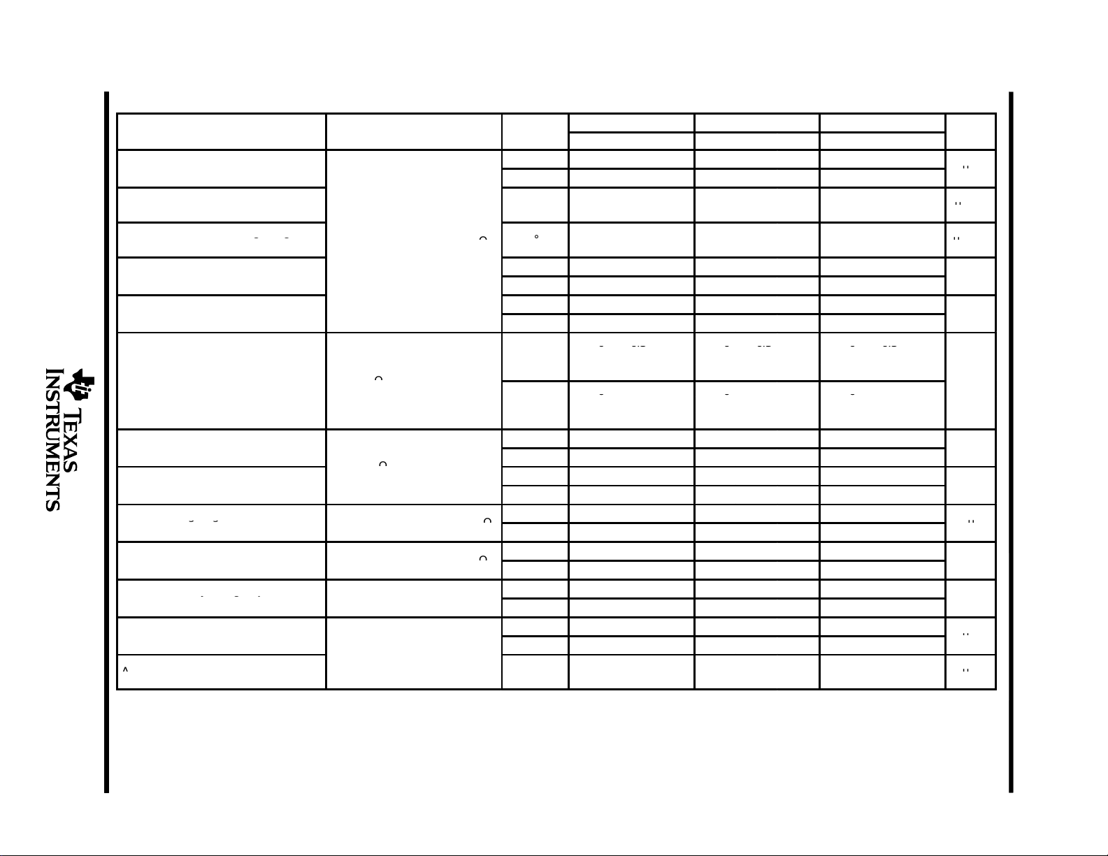
TLE2021 operating characteristics, VCC = 5 V, TA = 25°C
PARAMETER
TEST CONDITIONS
T
UNIT
V
qg
nV/Hz
V
q
V
PARAMETER
TEST CONDITIONS
T
†
UNIT
SR
Slew rate at unity gain
V
1V to 3 V
See Figure 1
V/µs
V
qg
nV/Hz
V
q
V
A
SR Slew rate at unity gain VO = 1 V to 3 V, See Figure 1 25°C 0.5 0.5 0.5 V/µs
n
N(PP)
I
n
B
1
φ
m
Equivalent input noise voltage
(see Figure 2)
Peak-to-peak equivalent input
noise voltage
Equivalent input noise current 25°C 0.09 0.09 0.9 pA/Hz
Unity-gain bandwidth See Figure 3 25°C 1.2 1.2 1.2 MHz
Phase margin at unity gain See Figure 3 25°C 42° 42° 42°
f = 10 Hz 25°C 21 50 21 50 21
f = 1 kHz
f = 0.1 to 1 Hz 25°C 0.16 0.16 0.16
f = 0.1 to 10 Hz
25°C 17 30 17 30 17
25°C 0.47 0.47 0.47
C SUFFIX I SUFFIX M SUFFIX
MIN TYP MAX MIN TYP MAX MIN TYP MAX
µ
POST OFFICE BOX 655303 DALLAS, TEXAS 75265
• 27
TLE2021 operating characteristics at specified free-air temperature, V
A
=
O
n
N(PP)
I
n
B
1
φ
m
†
Full range is 0°C to 70°C for the C-suffix devices, –40°C to 85°C for the I-suffix devices, and –55°C to 125°C for the M-suffix devices.
Equivalent input noise voltage
(see Figure 2)
Peak-to-peak equivalent input
noise voltage
Equivalent input noise current 25°C 0.09 0.09 0.09 pA/Hz
Unity-gain bandwidth See Figure 3 25°C 2 2 2 MHz
Phase margin at unity gain See Figure 3 25°C 46° 46° 46°
f = 10 Hz 25°C 19 50 19 50 19
f = 1 kHz
f = 0.1 to 1 Hz 25°C 0.16 0.16 0.16
f = 0.1 to 10 Hz
,
25°C 0.45 0.65 0.45 0.65 0.45 0.65
Full range 0.45 0.42 0.45
25°C 15 30 15 30 15
25°C 0.47 0.47 0.47
MIN TYP MAX MIN TYP MAX MIN TYP MAX
= ±15 V
CC
C SUFFIX I SUFFIX M SUFFIX
EXCALIBUR HIGH-SPEED LOW-POWER PRECISION
TLE202x, TLE202xA, TLE202xB, TLE202xY
µ
SLOS191B – FEBRUARY 1997 – REVISED JANUARY 2002
OPERATIONAL AMPLIFIERS
Page 28

28
PARAMETER
TEST CONDITIONS
UNIT
V
qg
V/√H
V
Peak-to-peak equivalent input noise voltage
V
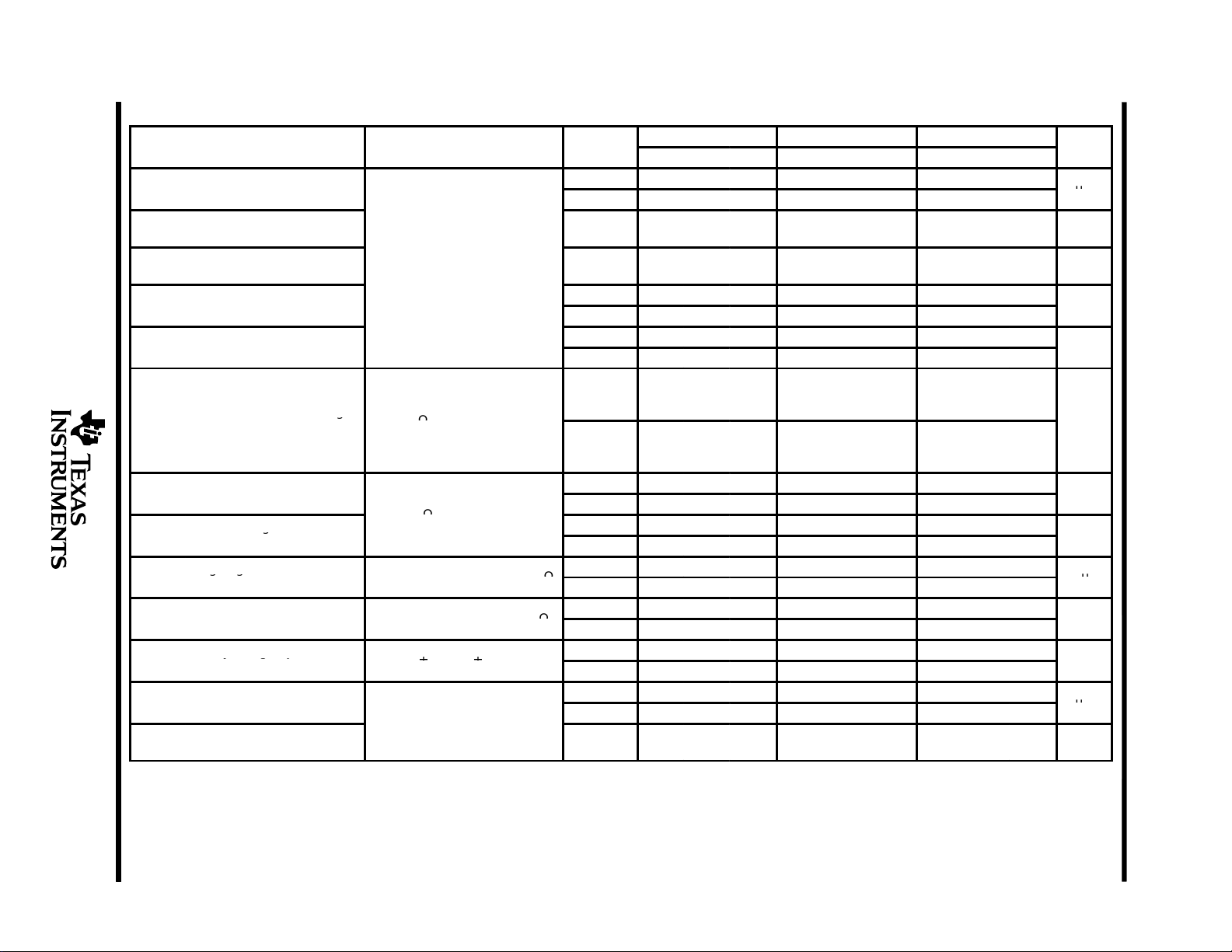
PARAMETER
TEST CONDITIONS
T
†
UNIT
SR
Slew rate at unity gain
V
±10 V
See Figure 1
V/µs
V
q
V/√H
V
q
V
TLE2022 operating characteristics, VCC = 5 V, TA = 25°C
C SUFFIX I SUFFIX M SUFFIX
MIN TYP MAX MIN TYP MAX MIN TYP MAX
SR Slew rate at unity gain VO = 1 V to 3 V, See Figure 1 0.5 0.5 0.5 V/µs
n
N(PP)
I
n
B
1
φ
m
Equivalent input noise voltage
(see Figure 2)
p
Equivalent input noise current 0.1 0.1 0.1
Unity-gain bandwidth See Figure 3 1.7 1.7 1.7 MHz
Phase margin at unity gain See Figure 3 47° 47° 47°
p
f = 10 Hz 21 50 21 50 21
f = 1 kHz
f = 0.1 to 1 Hz 0.16 0.16 0.16
f = 0.1 to 10 Hz 0.47 0.47 0.47
17 30 17 30 17
n
pA/√Hz
TLE202x, TLE202xA, TLE202xB, TLE202xY
EXCALIBUR HIGH-SPEED LOW-POWER PRECISION
OPERATIONAL AMPLIFIERS
SLOS191B – FEBRUARY 1997 – REVISED JANUARY 2002
z
µ
POST OFFICE BOX 655303 DALLAS, TEXAS 75265
•
TLE2022 operating characteristics at specified free-air temperature, VCC = ±15 V
C SUFFIX I SUFFIX M SUFFIX
MIN TYP MAX MIN TYP MAX MIN TYP MAX
n
N(PP)
I
n
B
1
φ
m
†
Full range is 0°C to 70°C.
Equivalent input noise
voltage (see Figure 2)
Peak-to-peak equivalent
input noise voltage
Equivalent input noise current 25°C 0.1 0.1 0.1 pA/√Hz
Unity-gain bandwidth See Figure 3 25°C 2.8 2.8 2.8 MHz
Phase margin at unity gain See Figure 3 25°C 52° 52° 52°
A
=
O
f = 10 Hz 25°C 19 50 19 50 19
f = 1 kHz
f = 0.1 to 1 Hz 25°C 0.16 0.16 0.16
f = 0.1 to 10 Hz
,
25°C 0.45 0.65 0.45 0.65 0.45 0.65
Full range 0.45 0.42 0.4
25°C 15 30 15 30 15
25°C 0.47 0.47 0.47
n
z
µ
Page 29

TLE2024 operating characteristics, VCC = 5 V, TA = 25°C
PARAMETER
TEST CONDITIONS
UNIT
VnEquivalent input noise voltage (see Figure 2)
V/√H
V
Peak-to-peak equivalent input noise voltage
V
PARAMETER
TEST CONDITIONS
T
†
UNIT
SR
Slew rate at unity gain
V
±10 V
See Figure 1
V/µs
V
qg
V/√H
V
q
V
C SUFFIX I SUFFIX M SUFFIX
MIN TYP MAX MIN TYP MAX MIN TYP MAX
SR Slew rate at unity gain VO = 1 V to 3 V, See Figure 1 0.5 0.5 0.5 V/µs
f = 10 Hz 21 50 21 50 21
f = 1 kHz 17 30 17 30 17
f = 0.1 to 1 Hz 0.16 0.16 0.16
f = 0.1 to 10 Hz 0.47 0.47 0.47
n
N(PP)
I
n
B
1
φ
m
p
p
Equivalent input noise current 0.1 0.1 0.1 pA/√Hz
Unity-gain bandwidth See Figure 3 1.7 1.7 1.7 MHz
Phase margin at unity gain See Figure 3 47° 47° 47°
p
z
µ
POST OFFICE BOX 655303 DALLAS, TEXAS 75265
• 29
TLE2024 operating characteristics at specified free-air temperature, V
C SUFFIX I SUFFIX M SUFFIX
MIN TYP MAX MIN TYP MAX MIN TYP MAX
n
N(PP)
I
n
B
1
φ
m
†
Full range is 0°C to 70°C.
Equivalent input noise voltage
(see Figure 2)
Peak-to-peak equivalent input noise
voltage
Equivalent input noise current 25°C 0.1 0.1 0.1 pA/√Hz
Unity-gain bandwidth See Figure 3 25°C 2.8 2.8 2.8 MHz
Phase margin at unity gain See Figure 3 25°C 52° 52° 52°
A
=
O
f = 10 Hz 25°C 19 50 19 50 19
f = 1 kHz
f = 0.1 to 1 Hz 25°C 0.16 0.16 0.16
f = 0.1 to 10 Hz
,
25°C 0.45 0.7 0.45 0.7 0.45 0.7
Full range 0.45 0.42 0.4
25°C 15 30 15 30 15
25°C 0.47 0.47 0.47
= ±15 V (unless otherwise noted)
CC
EXCALIBUR HIGH-SPEED LOW-POWER PRECISION
n
z
TLE202x, TLE202xA, TLE202xB, TLE202xY
µ
SLOS191B – FEBRUARY 1997 – REVISED JANUARY 2002
OPERATIONAL AMPLIFIERS
Page 30

TLE202x, TLE202xA, TLE202xB, TLE202xY
PARAMETER
TEST CONDITIONS
UNIT
V
0
R
50 Ω
R
10 kΩ
PARAMETER
TEST CONDITIONS
UNIT
VnEquivalent input noise voltage
V/√H
V
Peak-to-peak equivalent input noise voltage
V
EXCALIBUR HIGH-SPEED LOW-POWER PRECISION
OPERATIONAL AMPLIFIERS
SLOS191B – FEBRUARY 1997 – REVISED JANUARY 2002
TLE2021Y electrical characteristics at VCC= 5 V, TA = 25°C (unless otherwise noted)
TLE2021Y
MIN TYP MAX
V
I
IO
I
IB
V
V
V
A
CMRR Common-mode rejection ratio VIC = V
k
I
CC
NOTE 4: Typical values are based on the input offset voltage shift observed through 168 hours of operating life test at TA = 150°C extrapolated
Input offset voltage 150 µV
IO
Input offset voltage long-term drift (see Note 4)
Input offset current
Input bias current 35 nA
Common-mode input voltage range RS = 50 Ω
ICR
Maximum high-level output voltage
OH
Maximum low-level output voltage
OL
Large-signal differential voltage amplification VO = 1.4 to 4 V, RL = 10 kΩ 1.5 V/µV
VD
Supply-voltage rejection ratio (∆V
SVR
Supply current VO = 2.5 V, No load 400 µA
to TA = 25°C using the Arrhenius equation and assuming an activation energy of 0.96 eV .
/∆VIO) VCC = 5 V to 30 V 115 dB
CC±
,
=
IC
=
L
min, RS = 50 Ω 100 dB
ICR
=
S
0.005 µV/mo
0.5 nA
– 0.3
4.3 V
0.7 V
to
4
V
TLE2021Y operating characteristics at VCC= 5 V, TA = 25°C
TLE2021Y
MIN TYP MAX
SR Slew rate at unity gain VO = 1 V to 3 V 0.5 V/µs
f = 10 Hz 21
f = 1 kHz 17
f = 0.1 to 1 Hz 0.16
f = 0.1 to 10 Hz 0.47
n
pA/√Hz
N(PP)
I
n
B
1
φ
m
p
p
Equivalent input noise current 0.1
Unity-gain bandwidth 1.7 MHz
Phase margin at unity gain 47°
p
z
µ
30
POST OFFICE BOX 655303 • DALLAS, TEXAS 75265
Page 31

TLE202x, TLE202xA, TLE202xB, TLE202xY
PARAMETER
TEST CONDITIONS
UNIT
V
0
R
50 Ω
R
10 kΩ
PARAMETER
TEST CONDITIONS
UNIT
VnEquivalent input noise voltage (see Figure 2)
V/√H
V
Peak-to-peak equivalent input noise voltage
V
EXCALIBUR HIGH-SPEED LOW-POWER PRECISION
OPERATIONAL AMPLIFIERS
SLOS191B – FEBRUARY 1997 – REVISED JANUARY 2002
TLE2022Y electrical characteristics, VCC= 5 V, TA = 25°C (unless otherwise noted)
TLE2022Y
MIN TYP MAX
V
I
IO
I
IB
V
V
V
A
CMRR Common-mode rejection ratio VIC = V
k
I
CC
NOTE 4: Typical values are based on the input offset voltage shift observed through 168 hours of operating life test at TA = 150°C extrapolated
Input offset voltage 150 600 µV
IO
Input offset voltage long-term drift (see Note 4)
Input offset current
Input bias current 35 nA
Common-mode input voltage range RS = 50 Ω
ICR
Maximum high-level output voltage
OH
Maximum low-level output voltage
OL
Large-signal differential voltage amplification VO = 1.4 to 4 V, RL= 10 kΩ 1.5 V/µV
VD
Supply-voltage rejection ratio (∆V
SVR
Supply current VO = 2.5 V, No load 450 µA
to TA = 25°C using the Arrhenius equation and assuming an activation energy of 0.96 eV .
/∆VIO) VCC = 5 V to 30 V 115 dB
CC±
,
=
IC
=
L
min, RS = 50 Ω 100 dB
ICR
=
S
0.005 µV/mo
0.5 nA
– 0.3
to
4.3 V
0.7 V
V
4
TLE2022Y operating characteristics, VCC= 5 V, TA = 25°C
TLE2022Y
MIN TYP MAX
SR Slew rate at unity gain VO = 1 V to 3 V, See Figure 1 0.5 V/µs
f = 10 Hz 21
f = 1 kHz 17
f = 0.1 to 1 Hz 0.16
f = 0.1 to 10 Hz 0.47
n
pA/√Hz
N(PP)
I
n
B
1
φ
m
p
p
Equivalent input noise current 0.1
Unity-gain bandwidth See Figure 3 1.7 MHz
Phase margin at unity gain See Figure 3 47°
p
z
µ
POST OFFICE BOX 655303 • DALLAS, TEXAS 75265
31
Page 32

TLE202x, TLE202xA, TLE202xB, TLE202xY
PARAMETER
TEST CONDITIONS
UNIT
R
10 kΩ
PARAMETER
TEST CONDITIONS
UNIT
VnEquivalent input noise voltage (see Figure 2)
V/√H
V
Peak-to-peak equivalent input noise voltage
V
EXCALIBUR HIGH-SPEED LOW-POWER PRECISION
OPERATIONAL AMPLIFIERS
SLOS191B – FEBRUARY 1997 – REVISED JANUARY 2002
TLE2024Y electrical characteristics, VCC= 5 V, TA = 25°C (unless otherwise noted)
TLE2024Y
MIN TYP MAX
Input offset voltage long-term drift (see Note 4) 0.005 µV/mo
I
IO
I
IB
V
ICR
V
OH
V
OL
A
VD
CMRR Common-mode rejection ratio VIC = V
k
SVR
I
CC
NOTE 4. Typical values are based on the input offset voltage shift observed through 168 hours of operating life test at TA = 150°C extrapolated
Input offset current
Input bias current 45 nA
Common-mode input voltage range RS = 50 Ω
High-level output voltage
Low-level output voltage
Large-signal differential
voltage amplification
Supply-voltage rejection ratio
(∆VCC/∆VIO)
Supply current VO = 2.5 V, No load 800 µA
to TA = 25°C using the Arrhenius equation and assuming an activation energy of 0.96 eV .
VIC = 0, RS = 50 Ω
=
L
VO = 1.4 V to 4 V, RL = 10 kΩ 1.5 V/µV
min, RS = 50 Ω 90 dB
ICR
VCC = 5 V to 30 V 112 dB
0.6 nA
–0.3
to
4
4.2 V
0.7 V
V
TLE2024Y operating characteristics, VCC = 5 V, TA = 25°C
TLE2024Y
MIN TYP MAX
SR Slew rate at unity gain VO = 1 V to 3 V, See Figure 1 0.5 V/µs
f = 10 Hz 21
f = 1 kHz 17
f = 0.1 to 1 Hz 0.16
f = 0.1 to 10 Hz 0.47
n
N(PP)
I
n
B
1
φ
m
p
p
Equivalent input noise current 0.1 pA/√Hz
Unity-gain bandwidth See Figure 3 1.7 MHz
Phase margin at unity gain See Figure 3 47°
p
z
µ
32
POST OFFICE BOX 655303 • DALLAS, TEXAS 75265
Page 33

TLE202x, TLE202xA, TLE202xB, TLE202xY
EXCALIBUR HIGH-SPEED LOW-POWER PRECISION
OPERATIONAL AMPLIFIERS
SLOS191B – FEBRUARY 1997 – REVISED JANUARY 2002
PARAMETER MEASUREMENT INFORMATION
20 kΩ
5 V
–
V
NOTE A: CL includes fixture capacitance.
2.5 V
+
I
30 pF
(see Note A)
(a) SINGLE SUPPLY
20 Ω
20 Ω
(a) SINGLE SUPPLY
2 kΩ
5 V
–
+
V
O
20 kΩ
V
I
Figure 1. Slew-Rate Test Circuit
V
O
20Ω
20 kΩ
15 V
–
+
–15 V
30 pF
(see Note A)
(b) SPLIT SUPPLY
–
+
–15 V
20 Ω
2 kΩ
15 V
V
20 kΩ
O
V
O
Figure 2. Noise-Voltage Test Circuit
10 kΩ
100 Ω
V
I
2.5 V
(a) SINGLE SUPPLY
NOTE A: CL includes fixture capacitance.
5 V
–
+
30 pF
(see Note A)
Figure 3. Unity-Gain Bandwidth and Phase-Margin Test Circuit
10 kΩ
(b) SPLIT SUPPLY
10 kΩ
15 V
V
I
V
O
100Ω
–
+
–15 V
30 pF
(see Note A)
(b) SPLIT SUPPLY
10 kΩ
V
O
POST OFFICE BOX 655303 • DALLAS, TEXAS 75265
33
Page 34

TLE202x, TLE202xA, TLE202xB, TLE202xY
EXCALIBUR HIGH-SPEED LOW-POWER PRECISION
OPERATIONAL AMPLIFIERS
SLOS191B – FEBRUARY 1997 – REVISED JANUARY 2002
PARAMETER MEASUREMENT INFORMATION
5 V
–
0.1 µF
V
I
NOTE A: CL includes fixture capacitance.
10 kΩ
+
10 kΩ
30 pF
(see Note A)
(a) SINGLE SUPPLY
V
10 kΩ
O
V
15 V
–
+
I
– 15 V
30 pF
(see Note A)
(b) SPLIT SUPPLY
V
10 kΩ
Figure 4. Small-Signal Pulse-Response Test Circuit
typical values
Typical values presented in this data sheet represent the median (50% point) of device parametric performance.
O
34
POST OFFICE BOX 655303 • DALLAS, TEXAS 75265
Page 35

TLE202x, TLE202xA, TLE202xB, TLE202xY
EXCALIBUR HIGH-SPEED LOW-POWER PRECISION
OPERATIONAL AMPLIFIERS
SLOS191B – FEBRUARY 1997 – REVISED JANUARY 2002
TYPICAL CHARACTERISTICS
Table of Graphs
FIGURE
V
IO
I
IB
I
I
V
OM
V
OH
V
OL
V
O(PP)
A
VD
I
OS
I
CC
CMRR Common-mode rejection ratio vs Frequency 44, 45, 46
SR Slew rate vs Free-air temperature 47, 48, 49
V
N(PP)
V
n
B
1
φ
m
Input offset voltage Distribution 5, 6, 7
Input bias current
Input current vs Differential input voltage 14
Maximum peak output voltage
High-level output voltage
Low-level output voltage
Maximum peak-to-peak output voltage vs Frequency 24, 25
Large-signal differential voltage amplification
Short-circuit output current
Supply current
Voltage-follower small-signal pulse response 50, 51
Voltage-follower large-signal pulse response 52 – 57
Peak-to-peak equivalent input noise voltage
Equivalent input noise voltage vs Frequency 60
Unity-gain bandwidth
Phase margin
Phase shift vs Frequency 26
vs Common-mode input voltage
vs Free-air temperature
vs Output current
vs Free-air temperature
vs High-level output current
vs Free-air temperature
vs Low-level output current
vs Free-air temperature
vs Frequency
vs Free-air temperature
vs Supply voltage
vs Free-air temperature
vs Supply voltage
vs Free-air temperature
0.1 to 1 Hz
0.1 to 10 Hz
vs Supply voltage
vs Free-air temperature
vs Supply voltage
vs Load capacitance
vs Free-air temperature
8, 9, 10
11, 12, 13
15, 16, 17
18
19, 20
21
22
23
26
27, 28, 29
30 – 33
34 – 37
38, 39, 40
41, 42, 43
58
59
61, 62
63, 64
65, 66
67, 68
69, 70
POST OFFICE BOX 655303 • DALLAS, TEXAS 75265
35
Page 36

TLE202x, TLE202xA, TLE202xB, TLE202xY
EXCALIBUR HIGH-SPEED LOW-POWER PRECISION
OPERATIONAL AMPLIFIERS
SLOS191B – FEBRUARY 1997 – REVISED JANUARY 2002
TYPICAL CHARACTERISTICS
Percentage of Units – %
DISTRIBUTION OF TLE2021
INPUT OFFSET VOLTAGE
20
231 Units Tested From 1 Wafer Lot
V
= ±15 V
CC±
TA = 25°C
16
P Package
12
8
4
0
–600
–450 –150 150 450
VIO – Input Offset Voltage – µV
Figure 5
DISTRIBUTION OF TLE2024
16
796 Amplifiers Tested From 1 Wafer Lot
V
TA = 25°C
N Package
12
INPUT OFFSET VOLTAGE
= ±15 V
CC±
DISTRIBUTION OF TLE2022
INPUT OFFSET VOLTAGE
20
398 Amplifiers Tested From 1 Wafer Lot
V
= ±15 V
CC±
TA = 25°C
16
P Package
12
8
Percentage of Units – %
4
3000–300
600
0
–400 –200 0
–600
VIO – Input Offset Voltage – µV
200
400 600
Figure 6
TLE2021
INPUT BIAS CURRENT
vs
–40
–35
–30
COMMON-MODE INPUT VOLTAGE
V
= ±15 V
CC±
TA = 25°C
36
Percentage of Units – %
–25
8
4
0
–1
–0.5 0 0.5
VIO – Input Offset Voltage – mV
1
Figure 7
POST OFFICE BOX 655303 • DALLAS, TEXAS 75265
IB
I
IIB – Input Bias Current – nA
–20
–15
–10
–5
0
–15
1050–5–10
VIC – Common-Mode Input Voltage – V
Figure 8
15
Page 37

TLE202x, TLE202xA, TLE202xB, TLE202xY
EXCALIBUR HIGH-SPEED LOW-POWER PRECISION
SLOS191B – FEBRUARY 1997 – REVISED JANUARY 2002
TYPICAL CHARACTERISTICS
OPERATIONAL AMPLIFIERS
IB
I
IIB – Input Bias Current – nA
–50
–45
–40
–35
–30
–25
–20
–15
TLE2022
INPUT BIAS CURRENT
vs
COMMON-MODE INPUT VOLTAGE
V
= ±15 V
CC±
TA = 25°C
–10 –5 0 5 10
VIC – Common-Mode Input Voltage – V
Figure 9
15
IB
IIB – Input Bias Current – nA
I
–60
–50
–40
–30
–20
–15
TLE2024
INPUT BIAS CURRENT
vs
COMMON-MODE INPUT VOLTAGE
V
= ±15 V
CC±
TA = 25°C
–10 –5 0510
VIC – Common-Mode Input Voltage – V
Figure 10
15
IB
I
IIB – Input Bias Current – nA
–35
–30
–25
–20
–15
–10
–5
0
–75
TLE2021
INPUT BIAS CURRENT
†
vs
FREE-AIR TEMPERATURE
V
CC±
VO = 0
VIC = 0
TA – Free-Air Temperature – °C
Figure 11
= ±15 V
1007550250–25–50
125
IB
IIB – Input Bias Current – nA
I
–50
–45
–40
–35
–30
–25
–20
TLE2022
INPUT BIAS CURRENT
vs
FREE-AIR TEMPERATURE
–75
–50 –25 0 25 50 75 100
TA – Free-Air Temperature – °C
Figure 12
V
CC±
VO = 0
VIC = 0
†
= ±15 V
125
†
Data at high and low temperatures are applicable only within the rated operating free-air temperature ranges of the various devices.
POST OFFICE BOX 655303 • DALLAS, TEXAS 75265
37
Page 38

TLE202x, TLE202xA, TLE202xB, TLE202xY
EXCALIBUR HIGH-SPEED LOW-POWER PRECISION
OPERATIONAL AMPLIFIERS
SLOS191B – FEBRUARY 1997 – REVISED JANUARY 2002
TYPICAL CHARACTERISTICS
IB
I
IIB – Input Bias Current – nA
–60
–50
–40
–30
–20
TLE2024
INPUT BIAS CURRENT
vs
FREE-AIR TEMPERATURE
–75
–50 –25 0 25 50 75 100
TA – Free-Air Temperature – °C
Figure 13
†
V
CC±
VO = 0
VIC = 0
= ±15 V
125
I
II – Input Current – mA
I
0.9
0.8
0.7
0.6
0.5
0.4
0.3
0.2
0.1
1
0
0
INPUT CURRENT
vs
DIFFERENTIAL INPUT VOLTAGE
V
= ±15 V
CC±
VIC = 0
TA = 25°C
|VID| – Differential Input Voltage – V
Figure 14
0.90.80.70.60.50.40.30.20.1
1
VOM – Maximum Peak Output Voltage – V
V
OM
16
14
12
10
MAXIMUM PEAK OUTPUT VOLTAGE
TLE2021
vs
OUTPUT CURRENT
V
V
8
6
4
2
0
OM–
0
2 4 6 8
IO – Output Current – mA
Figure 15
V
TA = 25°C
OM+
CC±
= ±15 V
10
OM
VOM| – Maximum Peak Output Voltage – V
|V
16
14
12
10
TLE2022
MAXIMUM PEAK OUTPUT VOLTAGE
vs
OUTPUT CURRENT
V
8
6
4
2
0
246
0
OM–
81012
|IO| – Output Current – mA
Figure 16
V
= ±15 V
CC±
TA = 25°C
V
OM+
14
†
Data at high and low temperatures are applicable only within the rated operating free-air temperature ranges of the various devices.
38
POST OFFICE BOX 655303 • DALLAS, TEXAS 75265
Page 39

TLE202x, TLE202xA, TLE202xB, TLE202xY
†
EXCALIBUR HIGH-SPEED LOW-POWER PRECISION
SLOS191B – FEBRUARY 1997 – REVISED JANUARY 2002
TYPICAL CHARACTERISTICS
OPERATIONAL AMPLIFIERS
V
VOM – Maximum Peak Output Voltage – V
OM
10
16
14
12
TLE2024
MAXIMUM PEAK OUTPUT VOLTAGE
vs
OUTPUT CURRENT
V
= ±5 V
CC±
TA = 25°C
V
V
OM–
8
6
4
2
0
0
246
IO – Output Current – mA
81012
OM+
14
VOM| – Maximum Peak Output Voltage – V
|V
OM
14.5
13.5
12.5
Figure 17
TLE2021
HIGH-LEVEL OUTPUT VOLTAGE
vs
HIGH-LEVEL OUTPUT CURRENT
5
VCC = 5 V
TA = 25°C
4
5
4
MAXIMUM PEAK OUTPUT VOLTAGE
vs
FREE-AIR TEMPERATURE
15
V
OM+
14
13
12
–75
V
CC±
RL = 10 kΩ
TA = 25°C
–50 –25 0 25 50 75 100
V
OM–
= ±15 V
TA – Free-Air Temperature – °C
Figure 18
TLE2022 AND TLE2024
HIGH-LEVEL OUTPUT VOLTAGE
vs
HIGH-LEVEL OUTPUT CURRENT
125
VCC = 5 V
TA = 25°C
V
VOH – High-Level Output Voltage – V
OH
3
2
1
0
0
–1 –2 –3 –4 –5 – 6
IOH – High-Level Output Current – mA
–7
Figure 19
†
Data at high and low temperatures are applicable only within the rated operating free-air temperature ranges of the various devices.
POST OFFICE BOX 655303 • DALLAS, TEXAS 75265
V
VOH – High-Level Output Voltage – V
OH
3
2
1
0
0
–2 –4 –6 – 8
IOH – High-Level Output Current – mA
Figure 20
–10
39
Page 40

TLE202x, TLE202xA, TLE202xB, TLE202xY
†
†
EXCALIBUR HIGH-SPEED LOW-POWER PRECISION
OPERATIONAL AMPLIFIERS
SLOS191B – FEBRUARY 1997 – REVISED JANUARY 2002
TYPICAL CHARACTERISTICS
VOH – High-Level Output Voltage – V
V
OH
4.8
4.6
4.4
4.2
HIGH-LEVEL OUTPUT VOLTAGE
vs
5
4
–75
FREE-AIR TEMPERATURE
VCC = 5 V
No Load
RL = 10 kΩ
–50 –25 0 25 50 75 100
TA – Free-Air Temperature – °C
Figure 21
LOW-LEVEL OUTPUT VOLTAGE
vs
FREE-AIR TEMPERATURE
1
125
LOW-LEVEL OUTPUT VOLTAGE
vs
LOW-LEVEL OUTPUT CURRENT
5
VCC = 5 V
TA = 25°C
4
3
2
1
OL
V
VOL – Low-Level Output Voltage – V
0
0
0.5 1 1.5 2 2.5
IOL – Low-Level Output Current – mA
3
Figure 22
MAXIMUM PEAK-TO-PEAK OUTPUT VOLTAGE
vs
FREQUENCY
5
IOL = 1 mA
0.75
IOL = 0
0.5
0.25
OL
V
VOL – Low-Level Output Voltage – V
V
= ±5 V
CC±
0
–75
–50 –25 0 25 50 75 100
TA – Free-Air Temperature – °C
125
Figure 23
†
Data at high and low temperatures are applicable only within the rated operating free-air temperature ranges of the various devices.
O(PP)
VOPP – Maximum Peak-to-Peak Output Voltage – V
V
4
3
2
1
VCC =5 V
RL = 10 kΩ
TA = 25°C
0
100
1 k 10 k 100 k
f – Frequency – Hz
Figure 24
1 M
40
POST OFFICE BOX 655303 • DALLAS, TEXAS 75265
Page 41

TLE202x, TLE202xA, TLE202xB, TLE202xY
ÁÁ
ÁÁ
ÁÁ
EXCALIBUR HIGH-SPEED LOW-POWER PRECISION
TYPICAL CHARACTERISTICS
MAXIMUM PEAK-TO-PEAK OUTPUT VOLTAGE
vs
FREQUENCY
30
25
20
15
10
V
= ± 15 V
CC ±
RL = 10 kΩ
TA = 25°C
1 k 10 k 100 k
f – Frequency – Hz
O(PP)
VOPP – Maximum Peak-to-Peak Output Voltage – V
V
5
0
100
SLOS191B – FEBRUARY 1997 – REVISED JANUARY 2002
OPERATIONAL AMPLIFIERS
1 M
LARGE-SIGNAL DIFFERENTIAL VOLTAGE
AMPLIFICATION AND PHASE SHIFT
120
100
80
A
VD
60
40
20
– Large-Signal Differential
Voltage Amplification – dB
VD
A
–20
0
10
RL = 10 kΩ
CL = 30 pF
TA = 25°C
Figure 25
vs
FREQUENCY
Phase Shift
V
= ±15 V
CC±
VCC = 5 V
f – Frequency – Hz
60°
80°
100°
120°
140°
Phase Shift
160°
180°
10 M
200°
1 M100 k10 k1 k100
Figure 26
POST OFFICE BOX 655303 • DALLAS, TEXAS 75265
41
Page 42

TLE202x, TLE202xA, TLE202xB, TLE202xY
EXCALIBUR HIGH-SPEED LOW-POWER PRECISION
OPERATIONAL AMPLIFIERS
SLOS191B – FEBRUARY 1997 – REVISED JANUARY 2002
TYPICAL CHARACTERISTICS
LARGE-SCALE DIFFERENTIAL VOLTAGE
FREE-AIR TEMPERATURE
10
RL = 10 kΩ
Vµ
8
V/
6
4
– Large-Signal Differential
Voltage Amplification –
VD
A
2
0
–75
TA – Free-Air Temperature – °C
TLE2021
AMPLIFICATION
vs
V
= ±15 V
CC±
VCC = 5 V
Figure 27
TLE2022
†
LARGE-SIGNAL DIFFERENTIAL VOLTAGE
AMPLIFICATION
†
vs
FREE-AIR TEMPERATURE
6
RL = 10 kΩ
5
V
= ±15 V
4
3
2
VD
Voltage Amplification – V/µV
A
AVD – Large-Signal Differential
1
1007550250–25–50
125
0
–75
–50 –25 0 25 50 75 100
TA – Free-Air Temperature – °C
CC±
VCC = 5 V
125
Figure 28
TLE2024
LARGE-SCALE DIFFERENTIAL VOLTAGE
AMPLIFICATION
vs
†
SHORT-CIRCUIT OUTPUT CURRENT
FREE-AIR TEMPERATURE
10
Vµ
8
V/
6
4
Voltage Amplification –
VD
2
A – Large-Signal Differential
0
–75
TA – Free-Air Temperature – °C
V
CC±
V
= ±5 V
CC±
RL = 10 kΩ
= ±15 V
1007550250–25–50
125
OS
IOS – Short-Circuit Output Current – mA
I
10
–2
–4
–6
–8
–10
8
6
4
2
0
VO = 0
TA = 25°C
0
|V
Figure 29
†
Data at high and low temperatures are applicable only within the rated operating free-air temperature ranges of the various devices.
TLE2021
vs
SUPPLY VOLTAGE
VID = 100 mV
| – Supply Voltage – V
CC±
Figure 30
VID = –100 mV
1412108642
16
42
POST OFFICE BOX 655303 • DALLAS, TEXAS 75265
Page 43

TLE202x, TLE202xA, TLE202xB, TLE202xY
EXCALIBUR HIGH-SPEED LOW-POWER PRECISION
SLOS191B – FEBRUARY 1997 – REVISED JANUARY 2002
TYPICAL CHARACTERISTICS
OPERATIONAL AMPLIFIERS
OS
I
IOS – Short-Circuit Output Current – mA
15
10
–5
–10
–15
TLE2022 AND TLE2024
SHORT-CIRCUIT OUTPUT CURRENT
vs
SUPPLY VOLTAGE
VO = 0
TA = 25°C
5
0
VID = 100 mV
0
2 4 6 8101214
|V
| – Supply Voltage – V
CC±
Figure 31
VID = –100 mV
16
OS
IOS – Short-Circuit Output Current – mA
I
12
–4
–8
– 12
8
4
0
TLE2021
SHORT-CIRCUIT OUTPUT CURRENT
vs
SUPPLY VOLTAGE
TA = 25°C
VID = –100 mV
VO = V
CC
VID = 100 mV
VO = 0
0
VCC – Supply Voltage – V
Figure 32
252015105
30
TLE2022 AND TLE2024
OS
I
IOS – Short-Circuit Output CUrrent – mA
15
10
–5
–10
–15
SHORT-CIRCUIT OUTPUT CURRENT
vs
SUPPLY VOLTAGE
TA = 25°C
5
0
0
VCC – Supply Voltage – V
VID = –100 mV
VO = V
CC
VID = 100 mV
VO = 0
252015105
30
OS
I
IOS – Short-Circuit Output Current – mA
– 2
– 4
– 6
– 8
SHORT-CIRCUIT OUTPUT CURRENT
FREE-AIR TEMPERATURE
8
VCC =5 V
6
4
2
0
– 75
– 50 – 25 02550 75 100
TA – Free-Air Temperature – °C
Figure 33
†
Data at high and low temperatures are applicable only within the rated operating free-air temperature ranges of the various devices.
TLE2021
vs
VID = –100 mV
VO = 5 V
VID = 100 mV
VO = 0
Figure 34
†
125
POST OFFICE BOX 655303 • DALLAS, TEXAS 75265
43
Page 44

TLE202x, TLE202xA, TLE202xB, TLE202xY
EXCALIBUR HIGH-SPEED LOW-POWER PRECISION
OPERATIONAL AMPLIFIERS
SLOS191B – FEBRUARY 1997 – REVISED JANUARY 2002
TYPICAL CHARACTERISTICS
OS
I
IOS – Short-Circuit Output Current – mA
–2
–4
–6
–8
–10
TLE2022 AND TLE2024
SHORT-CIRCUIT OUTPUT CURRENT
vs
FREE-AIR TEMPERATURE
6
VCC = 5 V
4
2
0
–75
–50 –25 0255075100
TA – Free-Air Temperature –°C
VID = –100 mV
VO = 5 V
VID = 100 mV
VO = 0
Figure 35
†
SHORT-CIRCUIT OUTPUT CURRENT
TLE2021
†
vs
FREE-AIR TEMPERATURE
12
V
= ±15 V
CC±
VO = 0
8
VID = –100 mV
VID = 100 mV
125
125
OS
I
IOS – Short-Circuit Output Current – mA
–4
–8
–12
4
0
–75
–50 –25
TA – Free-Air Temperature – °C
0 25 50 75 100
Figure 36
OS
I
IOS – Short-Circuit Output Current – mA
15
10
–5
–10
–15
TLE2022 AND TLE2024
SHORT-CIRCUIT OUTPUT CURRENT
vs
FREE-AIR TEMPERATURE
V
= ±15 V
CC±
VO = 0
5
VID = –100 mV
0
VID = 100 mV
–75
–50 –25 0 25 50 75 100
TA – Free-Air Temperature – °C
Figure 37
†
SUPPLY CURRENT
vs
SUPPLY VOLTAGE
TLE2021
125
Aµ
CC
ICC – Supply Current – ua
I
250
200
150
100
50
0
VO = 0
No Load
TA = 125°C
TA = 25°C
TA = –55°C
0
2 4 6 8 10 12 14
|V
| – Supply Voltage – V
CC±
16
Figure 38
†
Data at high and low temperatures are applicable only within the rated operating free-air temperature ranges of the various devices.
44
POST OFFICE BOX 655303 • DALLAS, TEXAS 75265
Page 45

TLE202x, TLE202xA, TLE202xB, TLE202xY
EXCALIBUR HIGH-SPEED LOW-POWER PRECISION
SLOS191B – FEBRUARY 1997 – REVISED JANUARY 2002
TYPICAL CHARACTERISTICS
OPERATIONAL AMPLIFIERS
Aµ
CC
ICC – Supply Current – ua
I
500
400
300
200
100
0
TLE2022
SUPPLY CURRENT
vs
SUPPLY VOLTAGE
VO = 0
No Load
TA = 25°C
TA = 125°C
TA = –55°C
0
2 4 6 8 10 12 14
|V
| – Supply Voltage – V
CC±
Figure 39
16
– Supply Current – µAI
CC
1000
800
600
400
200
0
0
VO = 0
No Load
TLE2024
SUPPLY CURRENT
vs
SUPPLY VOLTAGE
TA = 125°C
TA = 25°C
TA = –55°C
|V
| – Supply Voltage – V
CC±
Figure 40
162 4 6 8 10 12 14
TLE2021
SUPPLY CURRENT
†
vs
FREE-AIR TEMPERATURE
VO = 0
No Load
–50 –25 0 25 50 75 100
TA – Free-Air Temperature – °C
Aµ
CC
ICC – Supply Current – ua
I
225
200
175
150
125
100
75
50
25
FREE-AIR TEMPERATURE
VO = 0
No Load
0
–50 –25 0 25 50 75 100
–75
TA – Free-Air Temperature – °C
V
V
CC±
CC±
= ±15 V
= ± 2.5 V
125
Aµ
CC
ICC – Supply Current – ua
I
500
400
300
200
100
0
–75
Figure 41
†
Data at high and low temperatures are applicable only within the rated operating free-air temperature ranges of the various devices.
TLE2022
SUPPLY CURRENT
vs
V
CC±
V
= ±2.5 V
CC±
Figure 42
†
= ±15 V
125
POST OFFICE BOX 655303 • DALLAS, TEXAS 75265
45
Page 46

TLE202x, TLE202xA, TLE202xB, TLE202xY
EXCALIBUR HIGH-SPEED LOW-POWER PRECISION
OPERATIONAL AMPLIFIERS
SLOS191B – FEBRUARY 1997 – REVISED JANUARY 2002
TYPICAL CHARACTERISTICS
TLE2024
SUPPLY CURRENT
vs
FREE-AIR TEMPERATURE
1000
V
800
V
600
400
– Supply Current – µAI
CC
200
VO = 0
No Load
0
–75 125–50 –25 0 25 50 75 100
CC±
TA – Free-Air Temperature – °C
CC±
= ±2.5 V
Figure 43
†
= ±15 V
CMRR – Common-Mode Rejection Ratio – dB
120
100
80
60
40
20
TLE2021
COMMON-MODE REJECTION RATIO
vs
FREQUENCY
VCC = 5 V
TA = 25°C
0
10
f – Frequency – Hz
Figure 44
V
CC±
= ±15 V
1 M100 k10 k1 k100
10 M
CMRR – Common-Mode Rehection Ratio – dB
120
100
80
60
40
20
0
10
TLE2022
COMMON-MODE REJECTION RATIO
vs
FREQUENCY
TA = 25°C
V
= ±15 V
CC±
VCC = 5 V
100 1 k 10 k 100 k 1 M
f – Frequency – Hz
Figure 45
10 M
CMRR – Common-Mode Rejection Ratio – dB
120
100
80
60
40
20
TLE2024
COMMON-MODE REJECTION RATIO
vs
FREQUENCY
V
= ±15 V
CC±
VCC = 5 V
TA = 25°C
0
10
100 1 k 10 k 100 k 1 M
f – Frequency – Hz
Figure 46
10 M
†
Data at high and low temperatures are applicable only within the rated operating free-air temperature ranges of the various devices.
46
POST OFFICE BOX 655303 • DALLAS, TEXAS 75265
Page 47

TLE202x, TLE202xA, TLE202xB, TLE202xY
EXCALIBUR HIGH-SPEED LOW-POWER PRECISION
SLOS191B – FEBRUARY 1997 – REVISED JANUARY 2002
TYPICAL CHARACTERISTICS
OPERATIONAL AMPLIFIERS
sµ
SR – Slew Rate – V/us
0.8
0.6
0.4
0.2
1
0
–75
TLE2021
SLEW RATE
FREE-AIR TEMPERATURE
V
= ±15 V
CC±
VCC = 5 V
RL = 20 kΩ
CL = 30 pF
See Figure 1
TA – Free-Air Temperature – °C
Figure 47
vs
TLE2022
†
SLEW RATE
†
vs
FREE-AIR TEMPERATURE
1
0.8
V
= ±15 V
sµ
0.6
0.4
SR – Slew Rate – V/ us
0.2
RL = 20 kΩ
CL = 30 pF
See Figure 1
0
–75
1007550250–25–50
125
–50 –25 0 25 50 75 100
TA – Free-Air Temperature – °C
CC±
VCC = 5 V
125
Figure 48
sµ
V/
SR – Slew Rate – V/s
0.8
0.6
0.4
0.2
1
0
–75
TLE2024
SLEW RATE
†
vs
FREE-AIR TEMPERATURE
V
= ±15 V
CC±
VCC = 5 V
RL = 20 kΩ
CL = 30 pF
See Figure 1
–50 –25 0 25 50 75 100
TA – Free-Air Temperature – °C
Figure 49
125
O
V
VO – Output Voltage – mV
100
50
–50
–100
V
CC±
RL = 10 kΩ
CL = 30 pF
TA = 25°C
See Figure 4
0
VOLTAGE-FOLLOWER
SMALL-SIGNAL
PULSE RESPONSE
= ±15 V
t – Time – µs
Figure 50
40200
60
80
†
Data at high and low temperatures are applicable only within the rated operating free-air temperature ranges of the various devices.
POST OFFICE BOX 655303 • DALLAS, TEXAS 75265
47
Page 48

TLE202x, TLE202xA, TLE202xB, TLE202xY
EXCALIBUR HIGH-SPEED LOW-POWER PRECISION
OPERATIONAL AMPLIFIERS
SLOS191B – FEBRUARY 1997 – REVISED JANUARY 2002
TYPICAL CHARACTERISTICS
VOLTAGE-FOLLOWER
SMALL-SIGNAL
VOLTAGE-FOLLOWER LARGE-SIGNAL
PULSE RESPONSE
2.6
VCC = 5 V
RL = 10 kΩ
CL = 30 pF
TA = 25°C
2.55
See Figure 4
2.5
O
V
VO – Output Voltage – V
2.45
2.4
t – Time – µs
6040200
80
4
VCC = 5 V
RL = 10 kΩ
CL = 30 pF
TA = 25°C
3
See Figure 1
2
O
V
VO – Output Voltage – V
1
0
Figure 51
TLE2022
VOLTAGE-FOLLOWER LARGE-SIGNAL
PULSE RESPONSE
4
VCC = 5 V
RL = 10 kΩ
CL = 30 pF
TA = 25°C
See Figure 1
3
VOLTAGE-FOLLOWER LARGE-SCALE
4
V
= 5 V
CC±
RL = 10 kΩ
CL = 30 pF
TA = 25°C
See Figure 1
3
TLE2021
PULSE RESPONSE
0 20 40 60
t – Time – µs
Figure 52
TLE2024
PULSE RESPONSE
80
48
2
O
V
VO – Output Voltage – V
1
0
0 20 40 60
t – Time – µs
80
Figure 53
POST OFFICE BOX 655303 • DALLAS, TEXAS 75265
2
O
V
VO – Output Voltage – V
1
0
0 20 40 60
t – Time – µs
80
Figure 54
Page 49

TLE202x, TLE202xA, TLE202xB, TLE202xY
EXCALIBUR HIGH-SPEED LOW-POWER PRECISION
SLOS191B – FEBRUARY 1997 – REVISED JANUARY 2002
TYPICAL CHARACTERISTICS
OPERATIONAL AMPLIFIERS
TLE2021
VOLTAGE-FOLLOWER LARGE-SIGNAL
VOLTAGE-FOLLOWER LARGE-SIGNAL
PULSE RESPONSE
15
V
= ±15 V
CC±
RL = 10 kΩ
CL = 30 pF
10
TA = 25°C
See Figure 1
5
0
– 5
O
V
VO – Output Voltage – V
–10
–15
0
20 40 60
t – Time – µs
80
15
V
= ±15 V
CC±
RL = 10 kΩ
CL = 30 pF
10
TA = 25°C
See Figure 1
5
0
–5
O
V
VO – Output Voltage – V
–10
–15
Figure 55
TLE2022
PULSE RESPONSE
0 20 40 60
t – Time – µs
Figure 56
80
TLE2024
VOLTAGE-FOLLOWER LARGE-SIGNAL
PULSE RESPONSE
15
V
= ±15 V
CC±
RL = 10 kΩ
CL = 30 pF
10
TA = 25°C
See Figure 1
5
Vµ
0.5
0.4
0.3
0.2
PEAK-TO-PEAK EQUIVALENT
INPUT NOISE VOLTAGE
0.1 TO 1 Hz
V
= ±15 V
CC±
TA = 25°C
0.1
0
–5
O
V
VO – Output Voltage – V
–10
–15
20 40 60
0
t – Time – µs
80
Figure 57
POST OFFICE BOX 655303 • DALLAS, TEXAS 75265
VNPP – Peak-to-Peak Equivalent Input Noise Voltage – uV
N(PP)
V
– 0.1
– 0.2
– 0.3
– 0.4
– 0.5
0
0
1 2 3 4 5 6 7 8 9
t – Time – s
Figure 58
10
49
Page 50

TLE202x, TLE202xA, TLE202xB, TLE202xY
EXCALIBUR HIGH-SPEED LOW-POWER PRECISION
OPERATIONAL AMPLIFIERS
SLOS191B – FEBRUARY 1997 – REVISED JANUARY 2002
TYPICAL CHARACTERISTICS
Vµ
VNPP – Peak-to-Peak Equivalent Input Noise Voltage – uV
N(PP)
V
0.5
0.4
0.3
0.2
0.1
– 0.1
– 0.2
– 0.3
– 0.4
– 0.5
4
3
0
RL = 10 kΩ
CL = 30 pF
TA = 25°C
See Figure 3
PEAK-TO-PEAK EQUIVALENT
INPUT NOISE VOLTAGE
0.1 TO 10 Hz
V
= ±15 V
CC±
TA = 25°C
t – Time – s
Figure 59
TLE2021
UNITY-GAIN BANDWIDTH
vs
SUPPLY VOLTAGE
EQUIVALENT INPUT NOISE VOLTAGE
vs
FREQUENCY
200
nV/ Hz
160
120
80
40
n
Vn – Equivalent Input Noise Voltage – nVHz
V
987654321100
0
1
10 100 1 k
f – Frequency – Hz
V
= ±15 V
CC±
RS = 20 Ω
TA = 25°C
See Figure 2
10 k
Figure 60
TLE2022 AND TLE2024
UNITY-GAIN BANDWIDTH
vs
SUPPLY VOLTAGE
4
RL = 10 kΩ
CL = 30 pF
TA = 25°C
See Figure 3
3
50
1
B1 – Unity-Gain Bandwidth – MHz
B
2
1
0
0
2 4 6 8 10 12 14
|V
| – Supply Voltage – V
CC±
16
Figure 61
POST OFFICE BOX 655303 • DALLAS, TEXAS 75265
1
B
B1 – Unity-Gain Bandwidth – MHz
2
1
0
0
|V
| – Supply Voltage – V
CC±
1412108642
16
Figure 62
Page 51

TLE202x, TLE202xA, TLE202xB, TLE202xY
EXCALIBUR HIGH-SPEED LOW-POWER PRECISION
SLOS191B – FEBRUARY 1997 – REVISED JANUARY 2002
TYPICAL CHARACTERISTICS
OPERATIONAL AMPLIFIERS
1
B1 – Unity-Gain Bandwidth – MHz
B
TLE2021
UNITY-GAIN BANDWIDTH
vs
FREE-AIR TEMPERATURE
4
RL = 10 kΩ
CL = 30 pF
See Figure 3
3
V
CC±
2
1
VCC = 5 V
0
–75
–50 –25 0 25 50 75 100
TA – Free-Air Temperature – °C
Figure 63
= ±15 V
†
UNITY-GAIN BANDWIDTH
†
vs
FREE-AIR TEMPERATURE
TLE2022 AND TLE2024
4
RL = 10 kΩ
CL = 30 pF
See Figure 3
3
V
= ±15 V
CC±
2
VCC = 5 V
1
1
B
B1 – Unity-Gain Bandwidth – MHz
125
0
–75
TA – Free-Air Temperature – °C
1007550250–25–50
125
Figure 64
50°
48°
46°
44°
m
m – Phase Margin
φ
42°
40°
RL = 10 kΩ
CL = 30 pF
TA = 25°C
See Figure 3
0
TLE2021
PHASE MARGIN
vs
SUPPLY VOLTAGE
2 4 6 8 10 12 14
|V
| – Supply Voltage – V
CC±
Figure 65
16
55°
RL = 10 kΩ
CL = 30 pF
53°
51°
49°
m
m – Phase Margin
φ
47°
45°
TA = 25°C
See Figure 3
0
TLE2022 AND TLE2024
PHASE MARGIN
vs
SUPPLY VOLTAGE
|V
| – Supply Voltage – V
CC±
Figure 66
1412108642
16
†
Data at high and low temperatures are applicable only within the rated operating free-air temperature ranges of the various devices.
POST OFFICE BOX 655303 • DALLAS, TEXAS 75265
51
Page 52

TLE202x, TLE202xA, TLE202xB, TLE202xY
EXCALIBUR HIGH-SPEED LOW-POWER PRECISION
OPERATIONAL AMPLIFIERS
SLOS191B – FEBRUARY 1997 – REVISED JANUARY 2002
TYPICAL CHARACTERISTICS
60°
50°
40°
30°
m
m – Phase Margin
20°
φ
10°
0
0
TLE2021
PHASE MARGIN
vs
LOAD CAPACITANCE
V
= ±15 V
CC±
VCC = 5 V
20 40 60 80
CL – Load Capacitance – pF
Figure 67
RL = 10 kΩ
TA = 30 pF
See Figure 3
100
70°
60°
50°
VCC = 5 V
40°
30°
m
m – Phase Margin
φ
20°
10°
0°
0
TLE2022 AND TLE2024
PHASE MARGIN
vs
LOAD CAPACITANCE
RL = 10 kΩ
TA = 25°C
V
= ±15 V
CC±
CL – Load Capacitance – pF
See Figure 3
Figure 68
80604020
100
50°
48°
46°
44°
m
m – Phase Margin
φ
40°
38°
36°
RL = 10 kΩ
CL = 30 pF
See Figure 3
42°
–75
TLE2021
PHASE MARGIN
†
vs
FREE-AIR TEMPERATURE
V
= ±15 V
CC±
VCC = 5 V
–50 –25 0 25 50 75 100
TA – Free-Air Temperature – °C
Figure 69
125
54°
52°
50°
48°
46°
m
m – Phase Margin
φ
44°
RL = 10 kΩ
CL = 30 pF
42°
See Figure 3
40°
–75
TLE2022 AND TLE2024
PHASE MARGIN
†
vs
FREE-AIR TEMPERATURE
V
= ±15 V
CC±
VCC = 5 V
TA – Free-Air Temperature – °C
Figure 70
1007550250–25–50
125
†
Data at high and low temperatures are applicable only within the rated operating free-air temperature ranges of the various devices.
52
POST OFFICE BOX 655303 • DALLAS, TEXAS 75265
Page 53

TLE202x, TLE202xA, TLE202xB, TLE202xY
EXCALIBUR HIGH-SPEED LOW-POWER PRECISION
OPERATIONAL AMPLIFIERS
SLOS191B – FEBRUARY 1997 – REVISED JANUARY 2002
APPLICATION INFORMATION
voltage-follower applications
The TLE202x circuitry includes input-protection diodes to limit the voltage across the input transistors; however,
no provision is made in the circuit to limit the current if these diodes are forward biased. This condition can occur
when the device is operated in the voltage-follower configuration and driven with a fast, large-signal pulse. It
is recommended that a feedback resistor be used to limit the current to a maximum of 1 mA to prevent
degradation of the device. This feedback resistor forms a pole with the input capacitance of the device. For
feedback resistor values greater than 10 kΩ, this pole degrades the amplifier phase margin. This problem can
be alleviated by adding a capacitor (20 pF to 50 pF) in parallel with the feedback resistor (see Figure 71).
CF = 20 pF to 50 pF
IF ≤ 1 mA
R
F
V
CC+
–
V
O
V
I
+
V
CC–
Figure 71. Voltage Follower
Input offset voltage nulling
The TLE202x series offers external null pins that further reduce the input offset voltage. The circuit in
Figure 72 can be connected as shown if this feature is desired. When external nulling is not needed, the null
pins may be left disconnected.
IN –
IN +
OFFSET N1
Figure 72. Input Offset Voltage Null Circuit
–
+
5 kΩ
1 kΩ GND (single supply)
OFFSET N2
VCC – (split supply)
POST OFFICE BOX 655303 • DALLAS, TEXAS 75265
53
Page 54

TLE202x, TLE202xA, TLE202xB, TLE202xY
EXCALIBUR HIGH-SPEED LOW-POWER PRECISION
OPERATIONAL AMPLIFIERS
SLOS191B – FEBRUARY 1997 – REVISED JANUARY 2002
APPLICATION INFORMATION
macromodel information
Macromodel information provided was derived using Microsim Parts, the model generation software used
with Microsim PSpice. The Boyle macromodel (see Note 5) and subcircuit in Figure 73, Figure 74, and Figure
75 were generated using the TLE202x typical electrical and operating characteristics at 25°C. Using this
information, output simulations of the following key parameters can be generated to a tolerance of 20% (in most
cases):
D
D
Maximum positive output voltage swing
D
Maximum negative output voltage swing
D
Slew rate
D
Quiescent power dissipation
D
Input bias current
D
Open-loop voltage amplification
Unity-gain frequency
D
Common-mode rejection ratio
D
Phase margin
D
DC output resistance
D
AC output resistance
D
Short-circuit output current limit
NOTE 5: G. R. Boyle, B. M. Cohn, D. O. Pederson, and J. E. Solomon, “Macromodeling of Integrated Circuit Operational Amplifiers”, IEEE Journal
of Solid-State Circuits, SC-9, 353 (1974).
V
CC+
ree
re1
C1
rc1
V
IN–
IN+
CC–
rp
cee Iee
1
2
dp
13
Q1
11
re2
rc2
4
Q2
99
3
14
12
ve
egnd
9
+
+
vc
dc
de
54
+–
r2
–
53
–
6
gcm
vb
+
–
ga
C2
din
fb
7
vlim
ro2
8
5
90
+
hlim
–
+
–
ro1
OUT
dip
91
+
–
92
–
vinvip
+
Figure 73. Boyle Subcircuit
PSpice and Parts are trademarks of MicroSim Corporation.
54
POST OFFICE BOX 655303 • DALLAS, TEXAS 75265
Page 55

TLE202x, TLE202xA, TLE202xB, TLE202xY
EXCALIBUR HIGH-SPEED LOW-POWER PRECISION
OPERATIONAL AMPLIFIERS
SLOS191B – FEBRUARY 1997 – REVISED JANUARY 2002
.SUBCKT TLE2021 1 2 3 4 5
*
c1 11 12 6.244E–12
c2 6 7 13.4E–12
c3 87 0 10.64E–9
cpsr 85 86 15.9E–9
dcm+ 81 82 dx
dcm– 83 81 dx
dc 5 53 dx
de 54 5 dx
dlp 90 91 dx
dln 92 90 dx
dp 4 3 dx
ecmr 84 99 (2 99) 1
egnd 99 0 poly(2) (3,0) (4,0) 0 .5 .5
epsr 85 0 poly(1) (3,4) –60E–6 2.0E–6
ense 89 2 poly(1) (88,0) 120E–6 1
fb 7 99 poly(6) vb vc ve vlp vln vpsr 0 547.3E6
+ –50E7 50E7 50E7 –50E7 547E6
ga 6 0 11 12 188.5E–6
gcm 0 6 10 99 335.2E–12
gpsr 85 86 (85,86) 100E–6
grc1 4 1 1 (4,11) 1.885E–4
grc2 4 12 (4,12) 1.885E–4
gre1 13 10 (13,10) 6.82E–4
gre2 14 10 (14,10) 6.82E–4
hlim 90 0 vlim 1k
Figure 74. Boyle Macromodel for the TLE2021
.SUBCKT TLE2022 1 2 3 4 5
*
c1 11 12 6.814E–12
c2 6 7 20.00E–12
dc 5 53 dx
de 54 5 dx
dlp 90 91 dx
dln 92 90 dx
dp 4 3 dx
egnd 99 0 poly(2) (3,0) (4,0) 0 .5 .5
fb 7 99 poly(5) vb vc ve vlp vln 0
+ 45.47E6 –50E6 50E6 50E6 –50E6
ga 6 0 11 12 377.9E–6
gcm 0 6 10 99 7.84E–10
iee 3 10 DC 18.07E–6
hlim 90 0 vlim 1k
q1 11 2 13 qx
q2 12 1 14 qx
r2 6 9 100.0E3
hcmr 80 1 poly(2) vcm+ vcm– 0 1E2 1E2
irp 3 4 185E–6
iee 3 10 dc 15.67E–6
iio 2 0 2E–9
i1 88 0 1E–21
q1 11 89 13 qx
q2 12 80 14 qx
R2 6 9 100.0E3
rcm 84 81 1K
ree 10 99 14.76E6
rn1 87 0 2.55E8
rn2 87 88 11.67E3
ro1 8 5 62
ro2 7 99 63
vcm+ 82 99 13.3
vcm– 83 99 –14.6
vb 9 0 dc 0
vc 3 53 dc 1.300
ve 54 4 dc 1.500
vlim 7 8 dc 0
vlp 91 0 dc 3.600
vln 0 92 dc 3.600
vpsr 0 86 dc 0
.model dx d(is=800.0E–18)
.model qx pnp(is=800.0E–18 bf=270)
.ends
rc1 4 11 2.842E3
rc2 4 12 2.842E3
ge1 13 10 (10,13) 31.299E–3
ge2 14 10 (10,14) 31.299E–3
ree 10 99 11.07E6
ro1 8 5 250
ro2 7 99 250
rp 3 4 137.2E3
vb 9 0 dc 0
vc 3 53 dc 1.300
ve 54 4 dc 1.500
vlim 7 8 dc 0
vlp 91 0 dc 3
vln 0 92 dc 3
.model dx d(is=800.0E–18)
.model qx pnp(is=800.0E–18 bf=257.1)
.ends
Figure 75. Boyle Macromodel for the TLE2022
POST OFFICE BOX 655303 • DALLAS, TEXAS 75265
55
Page 56

TLE202x, TLE202xA, TLE202xB, TLE202xY
EXCALIBUR HIGH-SPEED LOW-POWER PRECISION
OPERATIONAL AMPLIFIERS
SLOS191B – FEBRUARY 1997 – REVISED JANUARY 2002
MECHANICAL INFORMATION
D (R-PDSO-G**) PLASTIC SMALL-OUTLINE PACKAGE
14 PIN SHOWN
14
1
0.069 (1,75) MAX
0.050 (1,27)
A
0.020 (0,51)
0.014 (0,35)
0.010 (0,25)
0.004 (0,10)
8
7
0.010 (0,25)
0.157 (4,00)
0.150 (3,81)
M
0.244 (6,20)
0.228 (5,80)
Seating Plane
0.004 (0,10)
PINS **
DIM
A MAX
A MIN
0.008 (0,20) NOM
Gage Plane
0°–8°
8
0.197
(5,00)
0.189
(4,80)
14
0.344
(8,75)
0.337
(8,55)
0.010 (0,25)
0.044 (1,12)
0.016 (0,40)
4040047/B 03/95
16
0.394
(10,00)
0.386
(9,80)
NOTES: A. All linear dimensions are in inches (millimeters).
B. This drawing is subject to change without notice.
C. Body dimensions do not include mold flash or protrusion, not to exceed 0.006 (0,15).
D. Four center pins are connected to die mount pad.
E. Falls within JEDEC MS-012
56
POST OFFICE BOX 655303 • DALLAS, TEXAS 75265
Page 57

TLE202x, TLE202xA, TLE202xB, TLE202xY
EXCALIBUR HIGH-SPEED LOW-POWER PRECISION
OPERATIONAL AMPLIFIERS
SLOS191B – FEBRUARY 1997 – REVISED JANUARY 2002
MECHANICAL INFORMATION
DB (R-PDSO-G**) PLASTIC SMALL-OUTLINE PACKAGE
28 PIN SHOWN
0,65
28
1
2,00 MAX
0,38
0,22
15
14
A
0,05 MIN
0,15
5,60
5,00
M
8,20
7,40
Seating Plane
0,10
0,15 NOM
Gage Plane
0°–8°
0,25
1,03
0,63
PINS **
DIM
A MAX
A MIN
NOTES: A. All linear dimensions are in millimeters.
B. This drawing is subject to change without notice.
C. Body dimensions do not include mold flash or protrusion not to exceed 0,15.
D. Falls within JEDEC MO-150
8
3,30
2,70
14
6,50
6,50
5,905,90
2016
7,50
6,90
24
8,50
28
10,50
9,907,90
30
10,50
9,90
38
12,90
12,30
4040065 /C 10/95
POST OFFICE BOX 655303 • DALLAS, TEXAS 75265
57
Page 58

TLE202x, TLE202xA, TLE202xB, TLE202xY
EXCALIBUR HIGH-SPEED LOW-POWER PRECISION
OPERATIONAL AMPLIFIERS
SLOS191B – FEBRUARY 1997 – REVISED JANUARY 2002
MECHANICAL INFORMATION
DW (R-PDSO-G**) PLASTIC SMALL-OUTLINE PACKAGE
16 PIN SHOWN
16
1
0.050 (1,27)
0.020 (0,51)
0.014 (0,35)
A
0.010 (0,25)
9
8
0.299 (7,59)
0.293 (7,45)
M
0.419 (10,65)
0.400 (10,15)
PINS **
DIM
A MAX
A MIN
0.010 (0,25) NOM
0°–8°
16
0.410
(10,41)
0.400
(10,16)
Gage Plane
20
0.510
(12,95)
0.500
(12,70)
24
0.610
(15,49)
0.600
(15,24)
0.010 (0,25)
0.050 (1,27)
0.016 (0,40)
28
0.710
(18,03)
0.700
(17,78)
0.104 (2,65) MAX
NOTES: A. All linear dimensions are in inches (millimeters).
B. This drawing is subject to change without notice.
C. Body dimensions do not include mold flash or protrusion not to exceed 0.006 (0,15).
D. Falls within JEDEC MS-013
0.012 (0,30)
0.004 (0,10)
Seating Plane
0.004 (0,10)
4040000/B 03/95
58
POST OFFICE BOX 655303 • DALLAS, TEXAS 75265
Page 59

TLE202x, TLE202xA, TLE202xB, TLE202xY
EXCALIBUR HIGH-SPEED LOW-POWER PRECISION
OPERATIONAL AMPLIFIERS
SLOS191B – FEBRUARY 1997 – REVISED JANUARY 2002
MECHANICAL INFORMATION
FK (S-CQCC-N**) LEADLESS CERAMIC CHIP CARRIER
28 TERMINAL SHOWN
A SQ
B SQ
19
20
22
23
24
25
21
12826 27
121314151618 17
0.020 (0,51)
0.010 (0,25)
MIN
0.342
(8,69)
0.442
0.640
0.739
0.938
1.141
A
0.358
(9,09)
0.458
(11,63)
0.660
(16,76)
0.761
(19,32)(18,78)
0.962
(24,43)
1.165
(29,59)
NO. OF
TERMINALS
**
11
10
9
8
7
6
5
432
20
28
44
52
68
84
0.020 (0,51)
0.010 (0,25)
(11,23)
(16,26)
(23,83)
(28,99)
MINMAX
0.307
(7,80)
0.406
(10,31)
0.495
(12,58)
0.495
(12,58)
0.850
(21,6)
1.047
(26,6)
0.080 (2,03)
0.064 (1,63)
B
MAX
0.358
(9,09)
0.458
(11,63)
0.560
(14,22)
0.560
(14,22)
0.858
(21,8)
1.063
(27,0)
0.055 (1,40)
0.045 (1,14)
0.028 (0,71)
0.022 (0,54)
0.050 (1,27)
NOTES: A. All linear dimensions are in inches (millimeters).
B. This drawing is subject to change without notice.
C. This package can be hermetically sealed with a metal lid.
D. The terminals are gold plated.
E. Falls within JEDEC MS-004
POST OFFICE BOX 655303 • DALLAS, TEXAS 75265
0.045 (1,14)
0.035 (0,89)
0.045 (1,14)
0.035 (0,89)
4040140/D 10/96
59
Page 60

TLE202x, TLE202xA, TLE202xB, TLE202xY
EXCALIBUR HIGH-SPEED LOW-POWER PRECISION
OPERATIONAL AMPLIFIERS
SLOS191B – FEBRUARY 1997 – REVISED JANUARY 2002
MECHANICAL INFORMATION
J (R-GDIP-T**) CERAMIC DUAL-IN-LINE PACKAGE
14 PIN SHOWN
14
1
B
0.100 (2,54)
0.070 (1,78)
0.065 (1,65)
0.045 (1,14)
8
C
7
0.020 (0,51) MIN
0.200 (5,08) MAX
PINS **
DIM
A MAX
A MIN
B MAX
B MIN
C MAX
C MIN
Seating Plane
0.310
(7,87)
0.290
(7,37)
0.785
(19,94)
0.755
(19,18)
0.280
(7,11)
0.245
(6,22)
0.310
(7,87)
0.290
(7,37)
0.785
(19,94)
0.755
(19,18)
0.300
(7,62)
0.245
(6,22)
0.310
(7,87)
0.290
(7,37)
0.910
(23,10)
0.300
(7,62)
0.245
(6,22)
A
20181614
0.310
(7,87)
0.290
(7,37)
0.975
(24,77)
0.930
(23,62)
0.300
(7,62)
0.245
(6,22)
22
0.410
(10,41)
0.390
(9,91)
1.100
(28,00)
0.388
(9,65)
0.100 (2,54)
0.023 (0,58)
0.015 (0,38)
NOTES: A. All linear dimensions are in inches (millimeters).
B. This drawing is subject to change without notice.
C. This package can be hermetically sealed with a ceramic lid using glass frit.
D. Index point is provided on cap for terminal identification only on press ceramic glass frit seal only.
E. Falls within MIL-STD-1835 GDIP1-T14, GDIP1-T16, GDIP1-T18, GDIP1-T20, and GDIP1-T22
0.130 (3,30) MIN
0°–15°
0.014 (0,36)
0.008 (0,20)
4040083/B 04/95
60
POST OFFICE BOX 655303 • DALLAS, TEXAS 75265
Page 61

TLE202x, TLE202xA, TLE202xB, TLE202xY
EXCALIBUR HIGH-SPEED LOW-POWER PRECISION
OPERATIONAL AMPLIFIERS
SLOS191B – FEBRUARY 1997 – REVISED JANUARY 2002
MECHANICAL INFORMATION
JG (R-GDIP-T8) CERAMIC DUAL-IN-LINE PACKAGE
0.400 (10,20)
0.355 (9,00)
58
0.280 (7,11)
0.245 (6,22)
14
0.065 (1,65)
0.045 (1,14)
0.310 (7,87)
0.020 (0,51) MIN
0.290 (7,37)
0.063 (1,60)
0.015 (0,38)
0.100 (2,54)
NOTES: A. All linear dimensions are in inches (millimeters).
B. This drawing is subject to change without notice.
C. This package can be hermetically sealed with a ceramic lid using glass frit.
D. Index point is provided on cap for terminal identification only on press ceramic glass frit seal only
E. Falls within MIL-STD-1835 GDIP1-T8
0.023 (0,58)
0.015 (0,38)
0.200 (5,08) MAX
Seating Plane
0.130 (3,30) MIN
0°–15°
0.015 (0,38)
0.008 (0,20)
4040107/B 04/95
POST OFFICE BOX 655303 • DALLAS, TEXAS 75265
61
Page 62

TLE202x, TLE202xA, TLE202xB, TLE202xY
EXCALIBUR HIGH-SPEED LOW-POWER PRECISION
OPERATIONAL AMPLIFIERS
SLOS191B – FEBRUARY 1997 – REVISED JANUARY 2002
MECHANICAL INFORMATION
N (R-PDIP-T**) PLASTIC DUAL-IN-LINE PACKAGE
16 PIN SHOWN
16
1
0.035 (0,89) MAX
PINS **
DIM
A
9
0.260 (6,60)
0.240 (6,10)
8
0.070 (1,78) MAX
0.020 (0,51) MIN
0.200 (5,08) MAX
A MAX
A MIN
Seating Plane
14
0.775
(19,69)
0.745
(18,92)
16
0.775
(19,69)
0.745
(18,92)
18
0.920
(23.37)
0.850
(21.59)
20
0.975
(24,77)
0.940
(23,88)
0.310 (7,87)
0.290 (7,37)
0.100 (2,54)
0.021 (0,53)
0.015 (0,38)
NOTES: A. All linear dimensions are in inches (millimeters).
B. This drawing is subject to change without notice.
C. Falls within JEDEC MS-001 (20 pin package is shorter then MS-001.)
0.010 (0,25)
M
0.125 (3,18) MIN
0°–15°
0.010 (0,25) NOM
14/18 PIN ONL Y
4040049/C 08/95
62
POST OFFICE BOX 655303 • DALLAS, TEXAS 75265
Page 63

TLE202x, TLE202xA, TLE202xB, TLE202xY
EXCALIBUR HIGH-SPEED LOW-POWER PRECISION
OPERATIONAL AMPLIFIERS
SLOS191B – FEBRUARY 1997 – REVISED JANUARY 2002
MECHANICAL INFORMATION
P (R-PDIP-T8) PLASTIC DUAL-IN-LINE PACKAGE
0.400 (10,60)
0.355 (9,02)
58
0.260 (6,60)
0.240 (6,10)
41
0.070 (1,78) MAX
0.020 (0,51) MIN
0.200 (5,08) MAX
0.125 (3,18) MIN
0.100 (2,54)
0.021 (0,53)
0.015 (0,38)
NOTES: A. All linear dimensions are in inches (millimeters).
B. This drawing is subject to change without notice.
C. Falls within JEDEC MS-001
0.010 (0,25)
M
0.310 (7,87)
0.290 (7,37)
Seating Plane
0°–15°
0.010 (0,25) NOM
4040082/B 03/95
POST OFFICE BOX 655303 • DALLAS, TEXAS 75265
63
Page 64

TLE202x, TLE202xA, TLE202xB, TLE202xY
EXCALIBUR HIGH-SPEED LOW-POWER PRECISION
OPERATIONAL AMPLIFIERS
SLOS191B – FEBRUARY 1997 – REVISED JANUARY 2002
MECHANICAL INFORMATION
PW (R-PDSO-G**) PLASTIC SMALL-OUTLINE PACKAGE
14 PIN SHOWN
0,65
14
1
1,20 MAX
A
7
0,10 MIN
0,32
0,19
8
6,70
4,50
4,30
6,10
M
0,13
Seating Plane
0,10
0,15 NOM
Gage Plane
0,25
0°–8°
0,75
0,50
PINS **
DIM
A MAX
A MIN
NOTES: A. All linear dimensions are in millimeters.
B. This drawing is subject to change without notice.
C. Body dimensions do not include mold flash or protrusion not to exceed 0,15.
D. Falls within JEDEC MO-153
8
3,10
2,90
14
5,10
4,90
16
5,10
20
6,60
6,404,90
24
7,90
7,70
28
9,80
9,60
4040064/D 10/95
64
POST OFFICE BOX 655303 • DALLAS, TEXAS 75265
Page 65

IMPORTANT NOTICE
Texas Instruments Incorporated and its subsidiaries (TI) reserve the right to make corrections, modifications,
enhancements, improvements, and other changes to its products and services at any time and to discontinue
any product or service without notice. Customers should obtain the latest relevant information before placing
orders and should verify that such information is current and complete. All products are sold subject to TI’s terms
and conditions of sale supplied at the time of order acknowledgment.
TI warrants performance of its hardware products to the specifications applicable at the time of sale in
accordance with TI’s standard warranty . Testing and other quality control techniques are used to the extent TI
deems necessary to support this warranty . Except where mandated by government requirements, testing of all
parameters of each product is not necessarily performed.
TI assumes no liability for applications assistance or customer product design. Customers are responsible for
their products and applications using TI components. T o minimize the risks associated with customer products
and applications, customers should provide adequate design and operating safeguards.
TI does not warrant or represent that any license, either express or implied, is granted under any TI patent right,
copyright, mask work right, or other TI intellectual property right relating to any combination, machine, or process
in which TI products or services are used. Information published by TI regarding third–party products or services
does not constitute a license from TI to use such products or services or a warranty or endorsement thereof.
Use of such information may require a license from a third party under the patents or other intellectual property
of the third party , or a license from TI under the patents or other intellectual property of TI.
Reproduction of information in TI data books or data sheets is permissible only if reproduction is without
alteration and is accompanied by all associated warranties, conditions, limitations, and notices. Reproduction
of this information with alteration is an unfair and deceptive business practice. TI is not responsible or liable for
such altered documentation.
Resale of TI products or services with statements different from or beyond the parameters stated by TI for that
product or service voids all express and any implied warranties for the associated TI product or service and
is an unfair and deceptive business practice. TI is not responsible or liable for any such statements.
Mailing Address:
Texas Instruments
Post Office Box 655303
Dallas, Texas 75265
Copyright 2002, Texas Instruments Incorporated
 Loading...