Page 1
查询TLC7528C供应商
TLC7528C, TLC7528E, TLC7528I
DUAL 8-BIT MULTIPLYING
DIGITAL-TO-ANALOG CONVERTERS
SLAS062B – JANUARY 1987 – REVISED MARCH 2000
D
Easily Interfaced to Microprocessors
D
On-Chip Data Latches
D
Monotonic Over the Entire A/D Conversion
Range
D
Interchangeable With Analog Devices
AD7528 and PMI PM-7528
D
Fast Control Signaling for Digital Signal
Processor (DSP) Applications Including
Interface With TMS320
D
Voltage-Mode Operation
D
CMOS Technology
KEY PERFORMANCE SPECIFICATIONS
Resolution
Linearity Error
Power Dissipation at VDD = 5 V
Settling Time at VDD = 5 V
Propagation Delay Time at VDD = 5 V
description
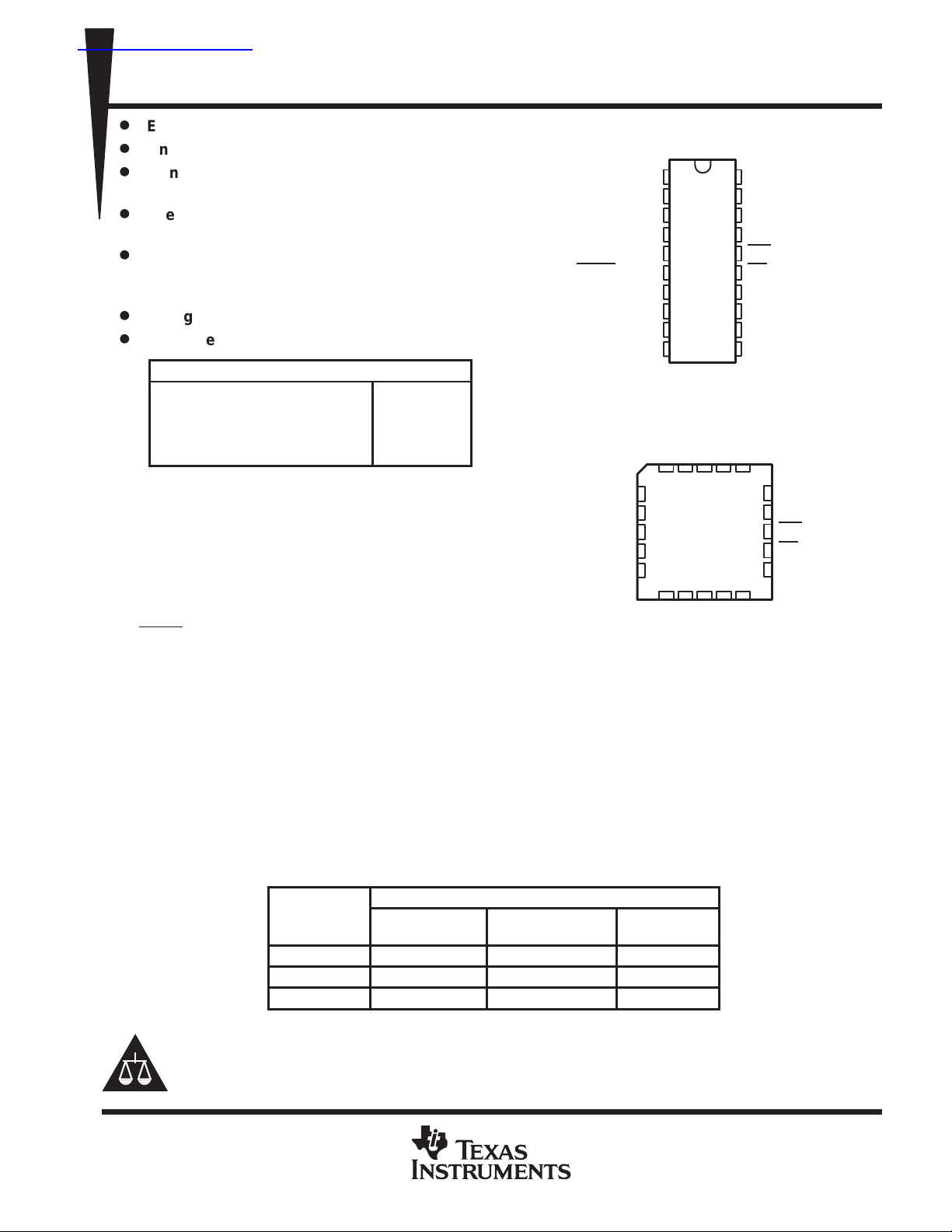
The TLC7528C, TLC7528E, and TLC7528I are
dual, 8-bit, digital-to-analog converters designed
with separate on-chip data latches and feature
exceptionally close DAC-to-DAC matching. Data
DACA
(MSB) DB7
8 bits
1/2 LSB
20 mW
100 ns
80 ns
REFA
DGND
DACA/DACB
(MSB) DB7
DW OR N PACKAGE
AGND
OUTA
RFBA
REFA
DGND
/DACB
DB6
DB5
DB4
FN PACKAGE
3212019
4
5
6
7
DB6
8
910111213
(TOP VIEW)
20
1
19
2
18
3
17
4
16
5
15
6
14
7
13
8
12
9
11
10
(TOP VIEW)
RFBA
OUTA
AGND
OUTB
RFBB
REFB
V
DD
WR
CS
DB0 (LSB)
DB1
DB2
DB3
OUTB
RFBB
18
17
16
15
14
REFB
V
DD
WR
CS
DB0 (LSB)
is transferred to either of the two DAC data latches
through a common, 8-bit, input port. Control input
DACA
/DACB determines which DAC is to be
DB5
DB4
DB3
DB2
DB1
loaded. The load cycle of these devices is similar
to the write cycle of a random-access memory , allowing easy interface to most popular microprocessor buses
and output ports. Segmenting the high-order bits minimizes glitches during changes in the most significant bits,
where glitch impulse is typically the strongest.
These devices operate from a 5-V to 15-V power supply and dissipates less than 15 mW (typical). The 2- or
4-quadrant multiplying makes these devices a sound choice for many microprocessor-controlled gain-setting
and signal-control applications. It can be operated in voltage mode, which produces a voltage output rather than
a current output. Refer to the typical application information in this data sheet.
The TLC7528C is characterized for operation from 0°C to 70°C. The TLC7528I is characterized for operation
from –25°C to 85°C. The TLC7528E is characterized for operation from –40°C to 85°C.
AVAILABLE OPTIONS
PACKAGE
T
A
0°C to 70°C TLC7528CDW TLC7528CFN TLC7528CN
–25°C to 85°C TLC7528IDW TLC7528IFN TLC7528IN
–40°C to 85°C TLC7528EDW TLC7528EFN TLC7528EN
Please be aware that an important notice concerning availability, standard warranty, and use in critical applications of
Texas Instruments semiconductor products and disclaimers thereto appears at the end of this data sheet.
PRODUCTION DATA information is current as of publication date.
Products conform to specifications per the terms of Texas Instruments
standard warranty. Production processing does not necessarily include
testing of all parameters.
SMALL OUTLINE
(DW)
POST OFFICE BOX 655303 • DALLAS, TEXAS 75265
CHIP CARRIER
(FN)
PLASTIC DIP
(N)
Copyright 2000, Texas Instruments Incorporated
1
Page 2
TLC7528C, TLC7528E, TLC7528I
DUAL 8-BIT MULTIPLYING
DIGITAL-TO-ANALOG CONVERTERS
SLAS062B – JANUARY 1987 – REVISED MARCH 2000
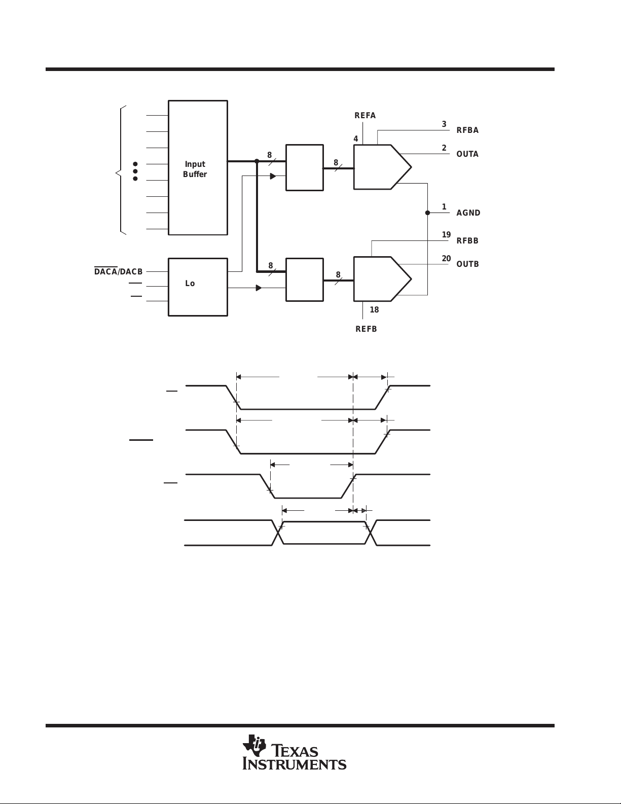
functional block diagram
DB0
Data
Inputs
DB7
DACA
/DACB
WR
CS
operating sequence
14
13
12
11
10
9
8
7
6
16
15
CS
Input
Buffer
Logic
Control
REFA
4
8
Latch A
8
Latch B
t
su(CS)
8
8
DACA
DACB
REFB
18
t
h(CS)
3
2
1
19
20
RFBA
OUTA
AGND
RFBB
OUTB
DACA/DACB
WR
DB0–DB7
t
su(DAC
t
w(WR)
t
su(D)
Data In Stable
)
t
h(D)
t
h(DAC)
2
POST OFFICE BOX 655303 • DALLAS, TEXAS 75265
Page 3
UNIT
TLC7528C, TLC7528E, TLC7528I
DUAL 8-BIT MULTIPLYING
DIGITAL-TO-ANALOG CONVERTERS
SLAS062B – JANUARY 1987 – REVISED MARCH 2000
absolute maximum ratings over operating free-air temperature range (unless otherwise noted)
Supply voltage range, VDD (to AGND or DGND) –0.3 V to 16.5 V. . . . . . . . . . . . . . . . . . . . . . . . . . . . . . . . . . . .
Voltage between AGND and DGND ±V
. . . . . . . . . . . . . . . . . . . . . . . . . . . . . . . . . . . . . . . . . . . . . . . . . . . . . . . . .
Input voltage range, VI (to DGND) –0.3 V to VDD + 0.3. . . . . . . . . . . . . . . . . . . . . . . . . . . . . . . . . . . . . . . . . . . . . .
Reference voltage, V
Feedback voltage V
refA
RFBA
or V
or V
(to AGND) ±25 V. . . . . . . . . . . . . . . . . . . . . . . . . . . . . . . . . . . . . . . . . . . . . . . . .
refB
(to AGND) ±25 V. . . . . . . . . . . . . . . . . . . . . . . . . . . . . . . . . . . . . . . . . . . . . . .
RFBB
Input voltage (voltage mode out A, out B to AGND) –0.3 V to VDD + 0.3. . . . . . . . . . . . . . . . . . . . . . . . . . . . . . .
Output voltage, VOA or VOB (to AGND) ±25 V. . . . . . . . . . . . . . . . . . . . . . . . . . . . . . . . . . . . . . . . . . . . . . . . . . . . . .
Peak input current 10 µA. . . . . . . . . . . . . . . . . . . . . . . . . . . . . . . . . . . . . . . . . . . . . . . . . . . . . . . . . . . . . . . . . . . . . . . .
Operating free-air temperature range, TA: TLC7528C 0°C to 70°C. . . . . . . . . . . . . . . . . . . . . . . . . . . . . . . . . . .
TLC7528I –25°C to 85°C. . . . . . . . . . . . . . . . . . . . . . . . . . . . . . . .
TLC7528E –40°C to 85°C. . . . . . . . . . . . . . . . . . . . . . . . . . . . . . . .
Storage temperature range, T
–65°C to 150°C. . . . . . . . . . . . . . . . . . . . . . . . . . . . . . . . . . . . . . . . . . . . . . . . . .
stg
Case temperature for 10 seconds, TC: FN package 260°C. . . . . . . . . . . . . . . . . . . . . . . . . . . . . . . . . . . . . . . . . .
Lead temperature 1,6 mm (1/16 inch) from case for 10 seconds: DW or N package 260°C. . . . . . . . . . . . . . .
†
Stresses beyond those listed under “absolute maximum ratings” may cause permanent damage to the device. These are stress ratings only, and
functional operation of the device at these or any other conditions beyond those indicated under “recommended operating conditions” is not
implied. Exposure to absolute-maximum-rated conditions for extended periods may affect device reliability.
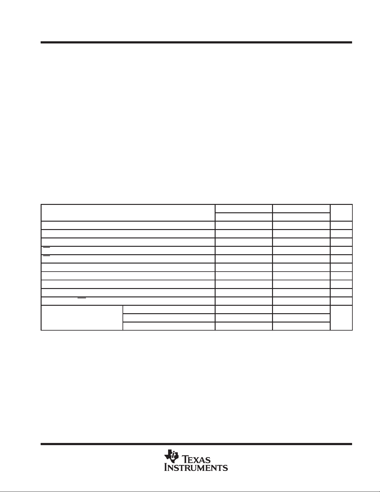
recommended operating conditions
VDD = 4.75 V to 5.25 V VDD = 14.5 V to 15.5 V
MIN NOM MAX MIN NOM MAX
Reference voltage, V
High-level input voltage, V
Low-level input voltage, V
CS setup time, t
CS hold time, t
DAC select setup time, t
DAC select hold time, t
Data bus input setup time t
Data bus input hold time t
Pulse duration, WR low, t
Operating free-air temperature, T
su(CS)
h(CS)
refA
su(DAC)
h(DAC)
or V
IH
IL
su(D)
h(D)
w(WR)
refB
TLC7628C 0 70 0 70
TLC7628I –25 85 –25 85
A
TLC7628E –40 85 –40 85
±10 ±10 V
2.4 13.5 V
0.8 1.5 V
50 50 ns
0 0 ns
50 50 ns
10 10 ns
25 25 ns
10 10 ns
50 50 ns
°C
†
DD
POST OFFICE BOX 655303 • DALLAS, TEXAS 75265
3
Page 4
TLC7528C, TLC7528E, TLC7528I
PARAMETER
TEST CONDITIONS
UNIT
I
Output leakage current
nA
CoOutput capacitance (OUTA, OUTB)
pF
DUAL 8-BIT MULTIPLYING
DIGITAL-TO-ANALOG CONVERTERS
SLAS062B – JANUARY 1987 – REVISED MARCH 2000
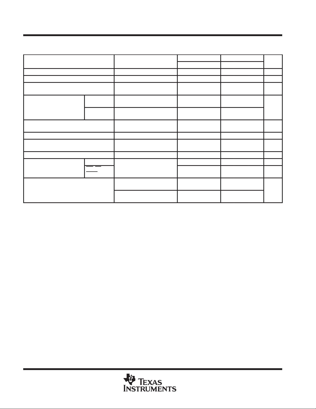
electrical characteristics over recommended operating free-air temperature range,
= V
V
refA
I
High-level input current VI = V
IH
I
Low-level input current VI = 0 5 12 –10 5 12 –10 µA
IL
Reference input impedance
REFA or REFB to AGND
Ikg
Input resistance match
(REFA to REFB)
DC supply sensitivity, ∆gain/∆V
I
Supply current (quiescent)
DD
I
Supply current (standby) All digital inputs at 0 V or V
DD
C
Input capacitance
i
†
All typical values are at TA = 25°C.
= 10 V, VOA and VOB at 0 V (unless otherwise noted)
refB
DD
OUTA
p
OUTB
DD
DB0–DB7 10 10 pF
WR
, CS,
DACA
/DACB
p
p
DAC data latch loaded with
00000000, V
DAC data latch loaded with
00000000, V
∆VDD = ±10% 0.04 0.02 %/%
All digital inputs at VIHmin or
VILmax
DAC data latches loaded with
00000000
DAC data latches loaded with
11111111
refA
refB
= ±10 V
= ±10 V
DD
VDD = 5 V VDD = 15 V
MIN TYP†MAX MIN TYP†MAX
10 10 µA
20 20 kΩ
±400 ±200
±400 ±200
±1% ±1%
2 2 mA
0.5 0.5 mA
15 15 pF
50 50
120 120
p
4
POST OFFICE BOX 655303 • DALLAS, TEXAS 75265
Page 5
PARAMETER
TEST CONDITIONS
UNIT
AC feedthrough
See Note 3
dB
dB
TLC7528C, TLC7528E, TLC7528I
DUAL 8-BIT MULTIPLYING
DIGITAL-TO-ANALOG CONVERTERS
SLAS062B – JANUARY 1987 – REVISED MARCH 2000
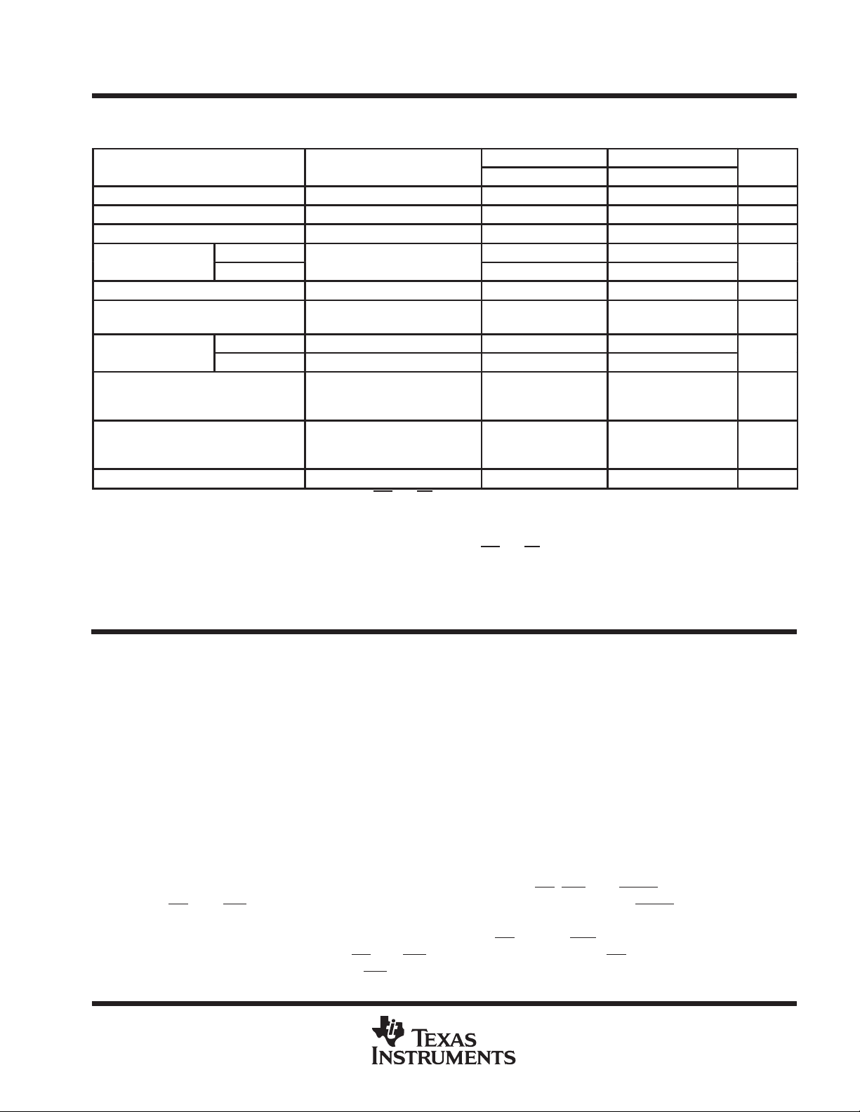
operating characteristics over recommended operating free-air temperature range,
= V
V
refA
Linearity error ±1/2 ±1/2 LSB
Settling time (to 1/2 LSB) See Note 1 100 100 ns
Gain error See Note 2 2.5 2.5 LSB
Temperature coefficient of gain See Note 4 0.007 0.0035 %FSR/°C
Propagation delay (from digital input to
90% of final analog output current)
Channel-to-channel
isolation
Digital-to-analog glitch impulse area
Digital crosstalk
Harmonic distortion Vi = 6 V, f = 1 kHz, TA = 25°C –85 –85 dB
NOTES: 1. OUTA, OUTB load = 100 Ω, C
= 10 V, VOA and VOB at 0 V (unless otherwise noted)
refB
VDD = 5 V VDD = 15 V
MIN TYP MAX MIN TYP MAX
REFA to OUTA
REFB to OUTB
See Note 5 80 80 ns
REFA to OUTB See Note 6 77 77
REFB to OUTA See Note 7 77 77
Measured for code transition
from 00000000 to 11111111,
TA = 25°C
Measured for code transition
from 00000000 to 11111111,
TA = 25°C
= 13 pF; WR and CS at 0 V; DB0–DB7 at 0 V to VDD or VDD to 0 V.
2. Gain error is measured using an internal feedback resistor. Nominal full scale range (FSR) = V
3. V
= 20 V peak-to-peak, 100-kHz sine wave; DAC data latches loaded with 00000000.
ref
4. Temperature coefficient of gain measured from 0°C to 25°C or from 25°C to 70°C.
5. V
6. Both DAC latches loaded with 11111111; V
7. Both DAC latches loaded with 11111111; V
refA
= V
= 10 V; OUTA/OUTB load = 100 Ω, C
refB
ext
= 13 pF; WR
ext
= 20 V peak-to-peak, 100-kHz sine wave; V
refA
= 20 V peak-to-peak, 100-kHz sine wave; V
refB
and CS at 0 V; DB0–DB7 at 0 V to VDD or VDD to 0 V.
–65 –65
–65 –65
160 440 nV•s
30 60 nV•s
refB
refA
– 1 LSB.
ref
= 0; TA = 25°C.
= 0; TA = 25°C.
PRINCIPLES OF OPERATION
These devices contain two identical, 8-bit-multiplying D/A converters, DACA and DACB. Each DAC consists
of an inverted R-2R ladder, analog switches, and input data latches. Binary-weighted currents are switched
between DAC output and AGND, thus maintaining a constant current in each ladder leg independent of the
switch state. Most applications require only the addition of an external operational amplifier and voltage
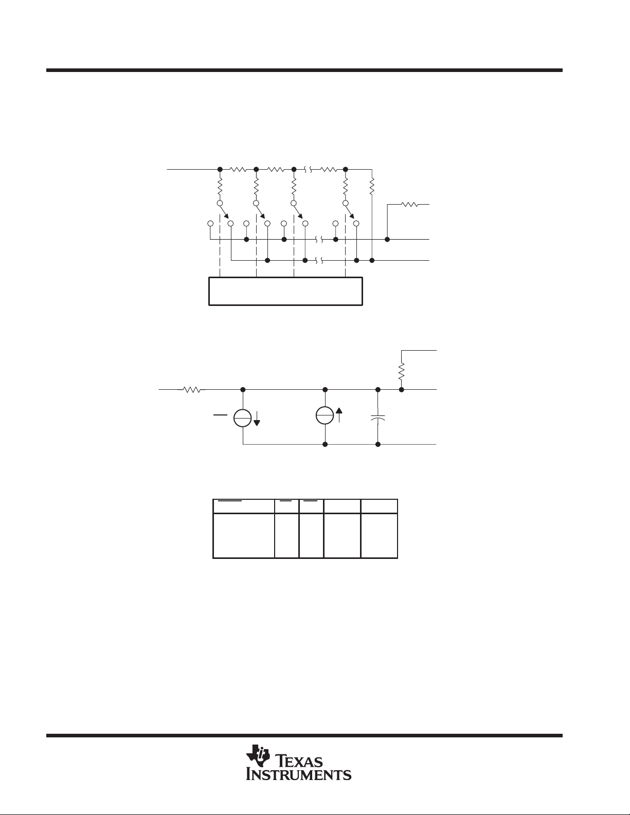
reference. A simplified D/A circuit for DACA with all digital inputs low is shown in Figure 1.
Figure 2 shows the DACA equivalent circuit. A similar equivalent circuit can be drawn for DACB. Both DACs
share the analog ground terminal 1 (AGND). With all digital inputs high, the entire reference current flows to
OUT A. A small leakage current (I
doubles every 10°C. C
is due to the parallel combination of the NMOS switches and has a value that depends
o
on the number of switches connected to the output. The range of Co is 50 pF to 120 pF maximum. The equivalent
output resistance (ro) varies with the input code from 0.8R to 3R where R is the nominal value of the ladder
resistor in the R-2R network.
These devices interface to a microprocessor through the data bus, CS, WR, and DACA/DACB control signals.
When CS and WR are both low, the TLC7528 analog output, specified by the DACA/DACB control line,
responds to the activity on the DB0–DB7 data bus inputs. In this mode, the input latches are transparent and
input data directly affects the analog output. When either the CS signal or WR signal goes high, the data on the
DB0–DB7 inputs is latched until the CS
disabled regardless of the state of the WR signal.
) flows across internal junctions, and as with most semiconductor devices,
Ikg
and WR signals go low again. When CS is high, the data inputs are
POST OFFICE BOX 655303 • DALLAS, TEXAS 75265
5
Page 6
TLC7528C, TLC7528E, TLC7528I
DUAL 8-BIT MULTIPLYING
DIGITAL-TO-ANALOG CONVERTERS
SLAS062B – JANUARY 1987 – REVISED MARCH 2000
PRINCIPLES OF OPERATION
The digital inputs of these devices provide TTL compatibility when operated from a supply voltage of 5 V . These
devices can operate with any supply voltage in the range from 5 V to 15 V; however, input logic levels are not
TTL compatible above 5 V.
REFA
REFA
RRR
2R
2R
S8
R
FB
S2
2R
S3
2R
DACA Data Latches and Drivers
2R
S1
Figure 1. Simplified Functional Circuit for DACA
C
R
OUT
R
I
256
I
Ikg
RFBA
OUTA
AGND
RFBA
FB
OUTA
AGND
Figure 2. TLC7528 Equivalent Circuit, DACA Latch Loaded With 11111111
MODE SELECTION TABLE
/DACB CS WR DACA DACB
DACA
L
H
X
X
L = low level, H = high level, X = don’t care
L
L
L
H
X
Write
L
Hold
X
Hold
H
Hold
Hold
Write
Hold
Hold
6
POST OFFICE BOX 655303 • DALLAS, TEXAS 75265
Page 7

TLC7528C, TLC7528E, TLC7528I
DUAL 8-BIT MULTIPLYING
DIGITAL-TO-ANALOG CONVERTERS
SLAS062B – JANUARY 1987 – REVISED MARCH 2000
APPLICATION INFORMATION
These devices are capable of performing 2-quadrant or full 4-quadrant multiplication. Circuit configurations for
2-quadrant and 4-quadrant multiplication are shown in Figures 3 and 4. T ables 1 and 2 summarize input coding
for unipolar and bipolar operation.
V
I(A)
±10 V
R1 (see Note A)
17
V
DD
14
DB0
DB7
7
DACA
/DACB
DGND
NOTES: A. R1, R2, R3, and R4 are used only if gain adjustment is required. See table for recommended values. Make gain adjustment with
B. C1 and C2 phase compensation capacitors (10 pF to 15 pF) are required when using high-speed amplifiers to prevent ringing or
6
15
CS
16
WR
5
digital input of 255.
oscillation.
Input
Buffer
Control
Logic
RECOMMENDED TRIM
RESISTOR VALUES
R1, R3
R2, R4
8
Latch
8
Latch
500 Ω
150 Ω
REFA
8
8
REFB
V
±10 V
RFBA
OUTA
DACA
AGND
RFBB
OUTB
DACB
AGND
R3 (see Note A)
I(B)
R2 (see Note A)
C1
(see Note B)
–
+
R4 (see Note A)
C2
(see Note B)
–
+
AGND
V
OA
V
OB
Figure 3. Unipolar Operation (2-Quadrant Multiplication)
POST OFFICE BOX 655303 • DALLAS, TEXAS 75265
7
Page 8

TLC7528C, TLC7528E, TLC7528I
ANALOG OUTPUT
ANALOG OUTPUT
DUAL 8-BIT MULTIPLYING
DIGITAL-TO-ANALOG CONVERTERS
SLAS062B – JANUARY 1987 – REVISED MARCH 2000
APPLICATION INFORMATION
V
I(A)
±10 V
(see Note A)
17
V
DD
14
DB0
DB7
DACA
DACB
NOTES: A. R1, R2, R3, and R4 are used only if gain adjustment is required. See table in Figure 3 for recommended values. Adjust R1 for
7
6
/
15
CS
16
WR
5
DGND
B. Matching and tracking are essential for resistor pairs R6, R7, R9, and R10.
C. C1 and C2 phase compensation capacitors (10 pF to 15 pF) may be required if A1 and A3 are high-speed amplifiers.
Input
Buffer
Control
Logic
VOA = 0 V with code 10000000 in DACA latch. Adjust R3 for VOB = 0 V with 10000000 in DACB latch.
Latch
Latch
R1
88
88
REFB
R3
(see Note A)
DACA
DACB
V
I(B)
±10 V
RFBA
OUTA
RFBB
OUTB
AGND
R2 (see Note A)
C1
(see Note C)
AGND
R4 (see Note A)
C2
(see Note C)
AGND
(see Note B)
R6
20 kΩ
(see Note B)
–
A1
+
–
A3
+
(see Note B)
R10
20 kΩ
R7
10 kΩ
(see Note B)
R11
5 kΩ
R9
10 kΩ
20 kΩ
–
A2
+
R8
20 kΩ
–
A4
+
R11
5 kΩ
AGND
R5
V
OA
V
OB
Table 1. Unipolar Binary Code Table 2. Bipolar (Offset Binary) Code
DAC LATCH CONTENTS
MSB LSB
1 1 1 1 1 1 1 1
1 0 0 0 0 0 0 1
1 0 0 0 0 0 0 0
0 1 1 1 1 1 1 1
0 0 0 0 0 0 0 1
0 0 0 0 0 0 0 0
†
1 LSB = (2–8)V
I
Figure 4. Bipolar Operation (4-Quadrant Operation)
DAC LATCH CONTENTS
†
–VI (255/256)
–VI (129/256)
–VI (128/256) = –Vi/2
–VI (127/256)
–VI (1/256)
–VI (0/256) = 0
MSB LSB
1 1 1 1 1 1 1 1
1 0 0 0 0 0 0 1
1 0 0 0 0 0 0 0
0 1 1 1 1 1 1 1
0 0 0 0 0 0 0 1
0 0 0 0 0 0 0 0
‡
1 LSB = (2–7)V
‡
VI (127/128)
VI (1/128)
0 V
–VI (1/128)
–VI (127/128)
–VI (128/128)
I
8
POST OFFICE BOX 655303 • DALLAS, TEXAS 75265
Page 9

APPLICATION INFORMATION
microprocessor interface information
A8–A15
TLC7528C, TLC7528E, TLC7528I
DUAL 8-BIT MULTIPLYING
DIGITAL-TO-ANALOG CONVERTERS
SLAS062B – JANUARY 1987 – REVISED MARCH 2000
8
Address Bus
Address
Decode
CPU
8051
WR
ALE
AD0–AD7
NOTE A: A = decoded address for TLC7528 DACA
A + 1 = decoded address for TLC7528 DACB
Logic
Latch
A
A + 1
8
Figure 5. TLC7528 – Intel 8051 Interface
8
A8–A15
VMA
CPU
6800
Address
Decode
Logic
Address Bus
A
A + 1
Data Bus
DACA/DACB
CS
TLC7528
WR
DB0
DB7
DACA/DACB
CS
TLC7528
WR
DB0
φ2
8
AD0–AD7
NOTE A: A = decoded address for TLC7528 DACA
A + 1 = decoded address for TLC7528 DACB
Data Bus
Figure 6. TLC7528 – 6800 Interface
POST OFFICE BOX 655303 • DALLAS, TEXAS 75265
DB7
9
Page 10

TLC7528C, TLC7528E, TLC7528I
DUAL 8-BIT MULTIPLYING
DIGITAL-TO-ANALOG CONVERTERS
SLAS062B – JANUARY 1987 – REVISED MARCH 2000
APPLICATION INFORMATION
A8–A15
IORQ
CPU
Z80-A
Address
Decode
Logic
8
Address Bus
A
A + 1
DACA
CS
TLC7528
WR
DB0
/DACB
WR
8
D0–D7
NOTE A: A = decoded address for TLC7528 DACA
A + 1 = decoded address for TLC7528 DACB
Data Bus
DB7
Figure 7. TLC7528 To Z-80A Interface
programmable window detector
The programmable window comparator shown in Figure 8 determines if voltage applied to the DAC feedback
resistors are within the limits programmed into the data latches of these devices. Input signal range depends
on the reference and polarity , that is, the test input range is 0 to –V
programmed with the upper and lower test limits. A signal within the programmed limits drives the output high.
. The DACA and DACB data latches are
ref
10
POST OFFICE BOX 655303 • DALLAS, TEXAS 75265
Page 11

TLC7528C, TLC7528E, TLC7528I
DUAL 8-BIT MULTIPLYING
DIGITAL-TO-ANALOG CONVERTERS
SLAS062B – JANUARY 1987 – REVISED MARCH 2000
APPLICATION INFORMATION
Test Input
0 to –V
ref
4
REFA
Data Inputs
V
8
ref
14–7
15
16
18
DB0–DB7
CS
WR
6
DACA
REFB
5
DGND
Figure 8. Digitally-Programmable Window Comparator (Upper- and Lower-Limit Tester)
digitally controlled signal attenuator
RFBA
DACA
TLC7528
/DACB
3
DACB
RFBB
19
V
OUTA 2
AGND
OUTB
DD
17
1
20
V
CC
1 kΩ
–
+
PASS/FAIL
–
+
Output
Figure 9 shows a TLC7528 configured as a two-channel programmable attenuator. Applications include stereo
audio and telephone signal level control. Table 3 shows input codes vs attenuation for a 0 to 15.5 dB range.
Attenuation dB = –20 log10 D/256, D = digital input code
VIA
VOB
A2
RFBA
OUTA
DB0–DB7
DACA/DACB
REFB
AGND
DGND
DD
17
20
19
REFA
4
OUTB
RFBB
DACA
TLC7528
DACB
V
CS
WR
3
2
14–7
15
16
6
18
1
5
OutputA1
8
Data Bus
Figure 9. Digitally Controlled Dual Telephone Attenuator
POST OFFICE BOX 655303 • DALLAS, TEXAS 75265
11
Page 12

TLC7528C, TLC7528E, TLC7528I
DUAL 8-BIT MULTIPLYING
DIGITAL-TO-ANALOG CONVERTERS
SLAS062B – JANUARY 1987 – REVISED MARCH 2000
APPLICATION INFORMATION
Table 3. Attenuation vs DACA, DACB Code
ATTN (dB) DAC INPUT CODE
0 1 1 1 1 1 1 1 1 255 8.0 0 1 1 0 0 1 1 0 102
0.5 1 1 1 1 0 0 1 0 242 8.5 0 1 1 0 0 0 0 0 96
1.0 1 1 1 0 0 1 0 0 228 9.0 0 1 0 1 1 0 1 1 91
1.5 1 1 0 1 0 1 1 1 215 9.5 0 1 0 1 0 1 1 0 86
2.0 1 1 0 0 1 0 1 1 203 10.0 0 1 0 1 0 0 0 1 81
2.5 1 1 0 0 0 0 0 0 192 10.5 0 1 0 0 1 1 0 0 76
3.0 1 0 1 1 0 1 0 1 181 11.0 0 1 0 0 1 0 0 0 72
3.5 1 0 1 0 1 0 1 1 171 11.5 0 1 0 0 0 1 0 0 68
4.0 1 0 1 0 0 0 1 0 162 12.0 0 1 0 0 0 0 0 0 64
4.5 1 0 0 1 1 0 0 0 152 12.5 0 0 1 1 1 1 0 1 61
5.0 1 0 0 1 1 1 1 1 144 13.0 0 0 1 1 1 0 0 1 57
5.5 1 0 0 0 1 0 0 0 136 13.5 0 0 1 1 0 1 1 0 54
6.0 1 0 0 0 0 0 0 0 128 14.0 0 0 1 1 0 0 1 1 51
6.5 0 1 1 1 1 0 0 1 121 14.5 0 0 1 1 0 0 0 0 48
7.0 0 1 1 1 0 0 1 0 114 15.0 0 0 1 0 1 1 1 0 46
7.5 0 1 1 0 1 1 0 0 108 15.5 0 0 1 0 1 0 1 1 43
CODE IN
DECIMAL
ATTN (dB) DAC INPUT CODE
CODE IN
DECIMAL
programmable state-variable filter
This programmable state-variable or universal filter configuration provides low-pass, high-pass, and bandpass
outputs, and is suitable for applications requiring microprocessor control of filter parameters.
As shown in Figure 10, DACA1 and DACB1 control the gain and Q of the filter while DACA2 and DACB2 control
the cutoff frequency. Both halves of the DACA2 and DACB2 must track accurately in order for the
cutoff-frequency equation to be true. With the TLC7528, this is easy to achieve.
fc+
The programmable range for the cutoff or center frequency is 0 to 15 kHz with a Q ranging from 0.3 to 4.5. This
defines the limits of the component values.
1
2pR1C1
12
POST OFFICE BOX 655303 • DALLAS, TEXAS 75265
Page 13

Data In
TLC7528C, TLC7528E, TLC7528I
DUAL 8-BIT MULTIPLYING
DIGITAL-TO-ANALOG CONVERTERS
SLAS062B – JANUARY 1987 – REVISED MARCH 2000
APPLICATION INFORMATION
C3
47 pF
4
17
14–7
15
16
5
6
REFA
V
CS
WR
DGND
DACA
DACA
DD
DB0–DB7
(RS)
TLC7528
DACB
(RF)
/DACB
DACA1 AND DACB1
AGND
V
I
8
OUTA
RFBA
OUTB
RFBB
REFB
2
3
1
20
19
18
C1
–
A1
+
R3
10 kΩ
Bandpass Out
–
A2
+
R5
30 kΩ
R4
30 kΩ
High Pass
Out
2
REFA
4
17
V
DD
8
Data In
Circuit Equations:
C1 = C2, R1 = R2, R4 = R
Q
+
Where:
Rfbis the internal resistor connected between OUTB and RFBB
G+–
NOTES: A. Op-amps A1, A2, A3, and A4 are TL287.
14–7
DB0–DB7
15
CS
16
WR
5
DGND
6
DACA/DACB
R
3
R
4
R
R
B. CS
C. DAC equivalent resistance equals
R
F
·
R
fb(DACB1)
F
S
compensates for the op-amp gain-bandwidth limitations.
DACA
(R1)
TLC7528
DACB
(R2)
DACA2 and DACB2
5
OUTA
3
RFBA
AGND
256 (DAC ladder resistance)
1
20
OUTB
19
RFBB
18
REFB
DAC digital code
Figure 10. Digitally Controlled State-Variable Filter
1000 pF
–
A3
+
C2
1000 pF
–
A4
+
Low Pass Out
POST OFFICE BOX 655303 • DALLAS, TEXAS 75265
13
Page 14

TLC7528C, TLC7528E, TLC7528I
DUAL 8-BIT MULTIPLYING
DIGITAL-TO-ANALOG CONVERTERS
SLAS062B – JANUARY 1987 – REVISED MARCH 2000
APPLICATION INFORMATION
voltage-mode operation
It is possible to operate the current multiplying D/A converter of these devices in a voltage mode. In the voltage
mode, a fixed voltage is placed on the current output terminal. The analog output voltage is then available at
the reference voltage terminal. Figure 1 1 is an example of a current multiplying D/A, that operates in the voltage
mode.
(Analog Output Voltage)
REF
RRR
2R 2R 2R
2R
“0” “1”
R
Out (Fixed Input Voltage)
AGND
Figure 11. Voltage-Mode Operation
The following equation shows the relationship between the fixed input voltage and the analog output voltage:
= VI (D/256)
V
O
Where:
VO = analog output voltage
VI = fixed input voltage (must not be forced below 0 V.)
D = digital input code converted to decimal
In voltage-mode operation, these devices meet the following specification:
PARAMETER TEST CONDITIONS MIN MAX UNIT
Linearity error at REFA or REFB VDD = 5 V, OUTA or OUTB at 2.5 V, TA = 25°C 1 LSB
14
POST OFFICE BOX 655303 • DALLAS, TEXAS 75265
Page 15

TLC7528C, TLC7528E, TLC7528I
DUAL 8-BIT MULTIPLYING
DIGITAL-TO-ANALOG CONVERTERS
SLAS062B – JANUARY 1987 – REVISED MARCH 2000
MECHANICAL DATA
DW (R-PDSO-G**) PLASTIC SMALL-OUTLINE PACKAGE
16 PINS SHOWN
0.050 (1,27)
16
1
0.020 (0,51)
0.014 (0,35)
9
0.299 (7,59)
0.291 (7,39)
8
A
0.010 (0,25)
0.419 (10,65)
0.400 (10,15)
M
0.010 (0,25) NOM
0°–8°
Gage Plane
0.010 (0,25)
0.050 (1,27)
0.016 (0,40)
0.104 (2,65) MAX
NOTES: A. All linear dimensions are in inches (millimeters).
B. This drawing is subject to change without notice.
C. Body dimensions do not include mold flash or protrusion not to exceed 0.006 (0,15).
D. Falls within JEDEC MS-013
0.012 (0,30)
0.004 (0,10)
DIM
A MAX
A MIN
PINS **
16
0.410
(10,41)
0.400
(10,16)
Seating Plane
0.004 (0,10)
20
0.510
(12,95)
0.500
(12,70)
0.610
(15,49)
0.600
(15,24)
24
28
0.710
(18,03)
0.700
(17,78)
4040000/D 01/00
POST OFFICE BOX 655303 • DALLAS, TEXAS 75265
15
Page 16

TLC7528C, TLC7528E, TLC7528I
DUAL 8-BIT MULTIPLYING
DIGITAL-TO-ANALOG CONVERTERS
SLAS062B – JANUARY 1987 – REVISED MARCH 2000
MECHANICAL DATA
N (R-PDIP-T**) PLASTIC DUAL-IN-LINE PACKAGE
16 PINS SHOWN
16
1
0.035 (0,89) MAX
A
0.070 (1,78) MAX
0.020 (0,51) MIN
9
8
0.260 (6,60)
0.240 (6,10)
0.200 (5,08) MAX
0.125 (3,18) MIN
PINS **
DIM
A MAX
A MIN
Seating Plane
14
0.775
(19,69)
0.745
(18,92)
16
0.775
(19,69)
0.745
(18,92)
0.325 (8,26)
0.300 (7,62)
18
0.920
(23,37)
0.850
(21,59)
0.015 (0,38)
Gauge Plane
0.010 (0,25) NOM
20
0.975
(24,77)
0.940
(23,88)
0.100 (2,54)
0.021 (0,53)
0.015 (0,38)
NOTES: A. All linear dimensions are in inches (millimeters).
B. This drawing is subject to change without notice.
C. Falls within JEDEC MS-001 (20-pin package is shorter than MS-001).
0.010 (0,25)
M
0.430 (10,92) MAX
14/18 PIN ONL Y
4040049/D 02/00
16
POST OFFICE BOX 655303 • DALLAS, TEXAS 75265
Page 17

IMPORTANT NOTICE
T exas Instruments and its subsidiaries (TI) reserve the right to make changes to their products or to discontinue
any product or service without notice, and advise customers to obtain the latest version of relevant information
to verify, before placing orders, that information being relied on is current and complete. All products are sold
subject to the terms and conditions of sale supplied at the time of order acknowledgement, including those
pertaining to warranty, patent infringement, and limitation of liability.
TI warrants performance of its semiconductor products to the specifications applicable at the time of sale in
accordance with TI’s standard warranty. Testing and other quality control techniques are utilized to the extent
TI deems necessary to support this warranty . Specific testing of all parameters of each device is not necessarily
performed, except those mandated by government requirements.
CERTAIN APPLICA TIONS USING SEMICONDUCT OR PRODUCTS MAY INVOLVE POTENTIAL RISKS OF
DEATH, PERSONAL INJURY, OR SEVERE PROPERTY OR ENVIRONMENTAL DAMAGE (“CRITICAL
APPLICATIONS”). TI SEMICONDUCTOR PRODUCTS ARE NOT DESIGNED, AUTHORIZED, OR
WARRANTED TO BE SUITABLE FOR USE IN LIFE-SUPPORT DEVICES OR SYSTEMS OR OTHER
CRITICAL APPLICA TIONS. INCLUSION OF TI PRODUCTS IN SUCH APPLICATIONS IS UNDERST OOD TO
BE FULLY AT THE CUSTOMER’S RISK.
In order to minimize risks associated with the customer’s applications, adequate design and operating
safeguards must be provided by the customer to minimize inherent or procedural hazards.
TI assumes no liability for applications assistance or customer product design. TI does not warrant or represent
that any license, either express or implied, is granted under any patent right, copyright, mask work right, or other
intellectual property right of TI covering or relating to any combination, machine, or process in which such
semiconductor products or services might be or are used. TI’s publication of information regarding any third
party’s products or services does not constitute TI’s approval, warranty or endorsement thereof.
Copyright 2000, Texas Instruments Incorporated
 Loading...