

Datasheet TLC7226IN, TLC7226IDWR, TLC7226IDW, TLC7226CN, TLC7226CDW Datasheet (Texas Instruments)
TLC7226C, TLC7226E
QUADRUPLE 8-BIT DIGITAL-TO-ANALOG CONVERTERS
SLAS060B – JANUARY 1995 – REVISED AUGUST 1996
features
D
Four 8-Bit D/A Converters
D
Microprocessor Compatible
D
TTL/CMOS Compatible
D
Single Supply Operation Possible
D
CMOS Technology
applications
D
Process Control
D
Automatic Test Equipment
D
Automatic Calibration of Large System
Parameters, e.g. Gain/Offset
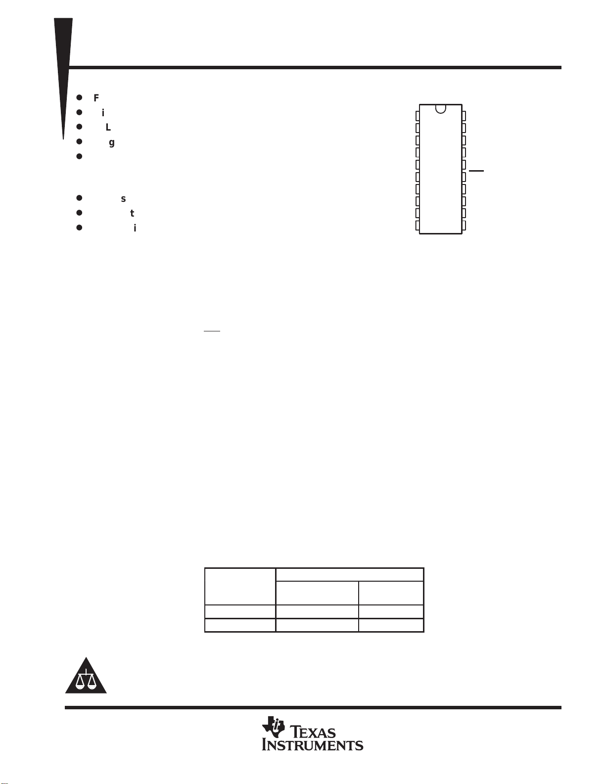
DW OR N PACKAGE
(TOP VIEW)
OUTB
OUTA
AGND
DGND
V
SS
REF
DB7
DB6
DB5
DB4
1
2
3
4
5
6
7
8
9
10
20
19
18
17
16
15
14
13
12
11
OUTC
OUTD
V
DD
A0
A1
WR
DB0
DB1
DB2
DB3
description
The TLC7226C and TLC7226E consist of four 8-bit voltage-output digital-to-analog converters (DACs) with
output buffer amplifiers and interface logic on a single monolithic chip.
Separate on-chip latches are provided for each of the four DACs. Data is transferred into one of these data
latches through a common 8-bit TTL/CMOS-compatible 5-V input port. Control inputs A0 and A1 determine
which DAC is loaded when WR
Each DAC includes an output buffer amplifier capable of sourcing up to 5 mA of output current.
goes low. The control logic is speed compatible with most 8-bit microprocessors.
The TLC7226 performance is specified for input reference voltages from 2 V to V
– 4 V with dual supplies.
DD
The voltage mode configuration of the DACs allows the TLC7226 to be operated from a single power supply
rail at a reference of 10 V.
The TLC7226 is fabricated in a LinBiCMOS process that has been specifically developed to allow high-speed
digital logic circuits and precision analog circuits to be integrated on the same chip. The TLC7226 has a common
8-bit data bus with individual DAC latches. This provides a versatile control architecture for simple interface to
microprocessors. All latch-enable signals are level triggered.
Combining four DACs, four operational amplifiers, and interface logic into either a 0.3-inch wide, 20-terminal
dual-in-line IC (DIP) or a small 20-terminal small-outline IC (SOIC) allows a dramatic reduction in board space
requirements and offers increased reliability in systems using multiple converters. The pinout is aimed at
optimizing board layout with all of the analog inputs and outputs at one end of the package and all of the digital
inputs at the other.
The TLC7226C is characterized for operation from 0°C to 70°C. The TLC7226E is characterized for operation
from –25°C to 85°C.
AVAILABLE OPTIONS
PACKAGE
T
A
0°C to 70°C TLC7226CDW TLC7226CN
–25°C to 85°C TLC7226EDW TLC7226EN
SMALL OUTLINE
(DW)
PLASTIC DIP
(N)
Please be aware that an important notice concerning availability, standard warranty, and use in critical applications of
Texas Instruments semiconductor products and disclaimers thereto appears at the end of this data sheet.
LinBiCMOS is a trademark of Texas Instruments Incorporated.
PRODUCTION DATA information is current as of publication date.
Products conform to specifications per the terms of Texas Instruments
standard warranty. Production processing does not necessarily include
testing of all parameters.
POST OFFICE BOX 655303 • DALLAS, TEXAS 75265
Copyright 1996, Texas Instruments Incorporated
1
TLC7226C, TLC7226E
QUADRUPLE 8-BIT DIGITAL-TO-ANALOG CONVERTERS
SLAS060B – JANUARY 1995 – REVISED AUGUST 1996
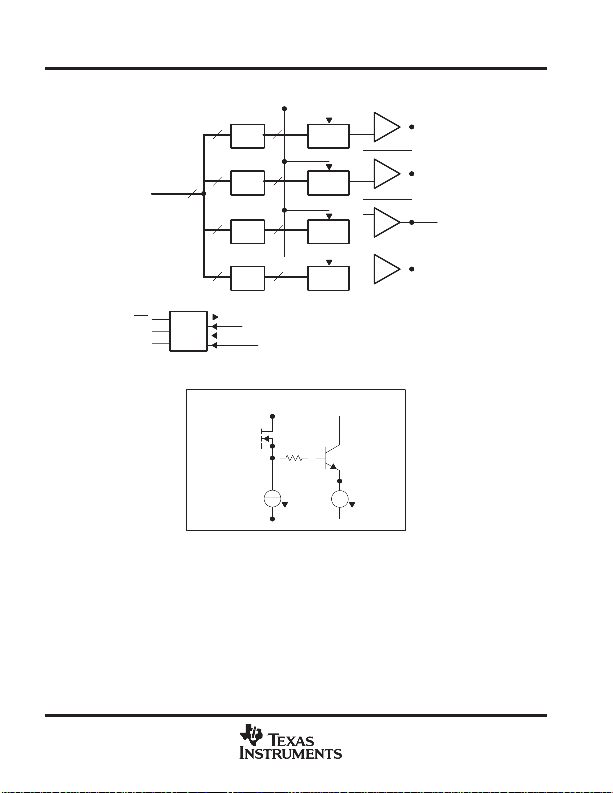
functional block diagram
4
REF
8
Latch
A
8
DAC A
_
+
2
OUTA
DB0–DB7
WR
A0
A1
schematic of outputs
7–14
15
17
16
8
Control
Logic
8
Latch
B
8
Latch
C
8
Latch
D
EQUIVALENT ANALOG OUTPUT
V
DD
8
8
8
DAC B
DAC C
DAC D
_
+
_
+
_
+
1
20
19
OUTB
OUTC
OUTD
Output
450 µA
V
SS
2
POST OFFICE BOX 655303 • DALLAS, TEXAS 75265
I/O
DESCRIPTION
TLC7226C, TLC7226E
QUADRUPLE 8-BIT DIGITAL-TO-ANALOG CONVERTERS
SLAS060B – JANUARY 1995 – REVISED AUGUST 1996
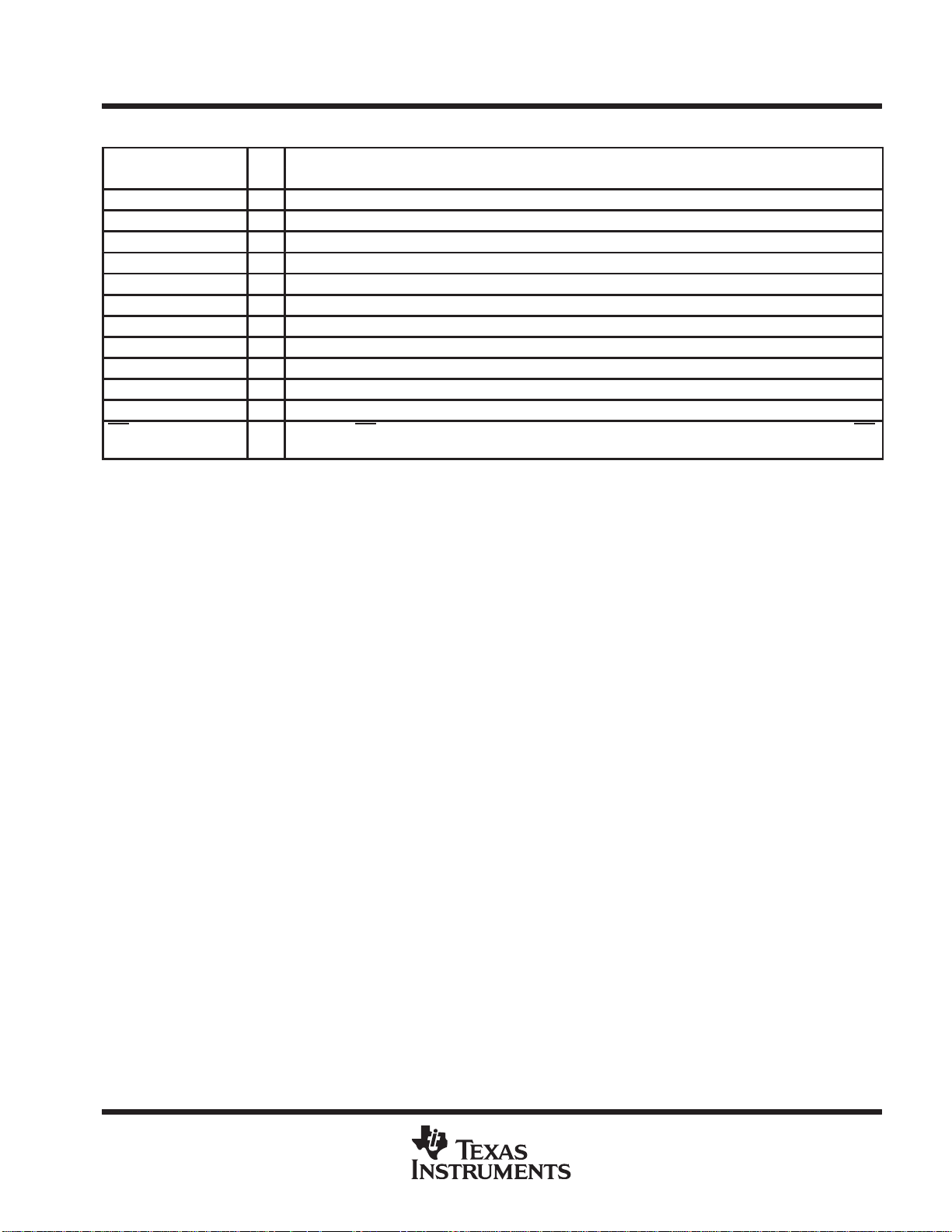
Terminal Functions
TERMINAL
NAME NO.
AGND 5 Analog ground. AGND is the reference and return terminal for the analog signals and supply.
A0, A1 16, 17 I DAC select inputs. The combination of high or low levels select either DACA, DACB, DACC, or DACD.
DGND 6 Digital ground. DGND is the reference and return terminal for the digital signals and supply.
DB0–DB7 7–14 I Digital DAC data inputs. DB0–DB7 are the input digital data used for conversion.
OUTA 2 O DACA output. OUTA is the analog output of DACA.
OUTB 1 O DACB output. OUTB is the analog output of DACB.
OUTC 20 O DACC output. OUTC is the analog output of DACC.
OUTD 19 O DACD output. OUTD is the analog output of DACD.
REF 4 I Voltage reference input. The voltage level on REF determines the full scale analog output.
V
DD
V
SS
WR 15 I Write input. WR selects DAC transparency or latch mode. The selected input latch is transparent when WR
†
Terminal numbers shown are for the DW and N packages.
†
18 Positive supply voltage input terminal
3 Negative supply voltage input terminal
is low.
POST OFFICE BOX 655303 • DALLAS, TEXAS 75265
3
TLC7226C, TLC7226E
Operating free-air temperature, T
QUADRUPLE 8-BIT DIGITAL-TO-ANALOG CONVERTERS
SLAS060B – JANUARY 1995 – REVISED AUGUST 1996
absolute maximum ratings over operating free-air temperature range (unless otherwise noted)
Supply voltage range, V
Supply voltage range, V
: AGND or DGND –0.3 V to 17 V. . . . . . . . . . . . . . . . . . . . . . . . . . . . . . . . . . . . . . . . .
DD
SS
‡
V
–0.3 V to 24 V. . . . . . . . . . . . . . . . . . . . . . . . . . . . . . . . . . . . . . . . . . . . . . . . . . .
SS
: AGND or DGND –7 V to 0.3 V. . . . . . . . . . . . . . . . . . . . . . . . . . . . . . . . . . . . . . . . . .
†
Voltage range between AGND and DGND –17 V to 17 V. . . . . . . . . . . . . . . . . . . . . . . . . . . . . . . . . . . . . . . . . . . .
Input voltage range, V
Reference voltage range: V
Output voltage range, V
Continuous total power dissipation at (or below) T
Operating free-air temperature range, T
(to DGND) –0.3 V to VDD + 0.3 V. . . . . . . . . . . . . . . . . . . . . . . . . . . . . . . . . . . . . . . . . . . .
I
O
(to AGND) –0.3 V to V
ref
V
(to VSS) –0.3 V to 20 V. . . . . . . . . . . . . . . . . . . . . . . . . . . . . . . . . . . . . . . . . . . . .
ref
(to AGND) (see Note 1) VSS to V
. . . . . . . . . . . . . . . . . . . . . . . . . . . . . . . . . . . . . . . . . . .
. . . . . . . . . . . . . . . . . . . . . . . . . . . . . . . . . . . . . . . .
= 25°C (see Note 2) 500 mW. . . . . . . . . . . . . . . . . . . . . . .
: C suffix 0°C to 70°C. . . . . . . . . . . . . . . . . . . . . . . . . . . . . . . . . . . . . . .
A
A
DD
DD
E suffix –25°C to 85°C. . . . . . . . . . . . . . . . . . . . . . . . . . . . . . . . . . . . .
Storage temperature range, T
–65°C to 150°C. . . . . . . . . . . . . . . . . . . . . . . . . . . . . . . . . . . . . . . . . . . . . . . . . . .
stg
Lead temperature 1,6 mm (1/16 inch) from case for 10 seconds: DW or N packages 260°C. . . . . . . . . . . . . .
†
Stresses beyond those listed under “absolute maximum ratings” may cause permanent damage to the device. These are stress ratings only, and
functional operation of the device at these or any other conditions beyond those indicated under “recommended operating conditions” is not
implied. Exposure to absolute-maximum-rated conditions for extended periods may affect device reliability.
‡
The VSS terminal is connected to the substrate and must be tied to the most negative supply voltage applied to the device.
NOTES: 1. Output voltages may be shorted to AGND provided that the power dissipation of the package is not exceeded. Typically sh ort circuit
current to AGND is 60 mA.
2. For operation above TA = 75°C, derate linearly at the rate of 2 mW/°C.
recommended operating conditions
MIN MAX UNIT
Supply voltage, V
Supply voltage, V
High-level input voltage, V
Low-level input voltage, V
Reference voltage, V
Load resistance, R
Setup time, address valid before WR↓, t
Setup time, data valid before WR↑, t
Hold time, address valid before WR↑, t
Hold time, data valid before WR↑, t
Pulse duration, WR low, tw (see Figure 6)
p
DD
SS
IH
IL
ref
L
su(DW)
h(AW)
h(DW)
p
A
(see Figure 6) VDD = 11.4 V to 16.5 V 0 ns
su(AW)
(see Figure 6)
(see Figure 6)
(see Figure 6)
VDD = 11.4 V to 16.5 V 45 ns
VDD = 11.4 V to 16.5 V 0 ns
VDD = 11.4 V to 16.5 V 10 ns
VDD = 11.4 V to 16.5 V 50 ns
C suffix 0 70 °C
E suffix –25 85 °C
11.4 16.5 V
–5.5 0 V
2 V
0.8 V
0 VDD–4 V
2 kΩ
4
POST OFFICE BOX 655303 • DALLAS, TEXAS 75265
REF input
Settling time to 1/2 LSB
V
V
s
V
±5%
V
V
Temperature coefficient of gain
Settling time to 1/2 LSB
s
Temperature coefficient of gain
TLC7226C, TLC7226E
QUADRUPLE 8-BIT DIGITAL-TO-ANALOG CONVERTERS
SLAS060B – JANUARY 1995 – REVISED AUGUST 1996
electrical characteristics over recommended operating free-air temperature range
dual power supply over recommended power supply and reference voltage ranges, AGND = DGND = 0 V
(unless otherwise noted)
PARAMETER TEST CONDITIONS MIN TYP MAX UNIT
I
I
I
DD
I
SS
r
i(ref)
C
i
operating characteristics over recommended operating free-air temperature range
dual power supply over recommended power supply and reference voltage ranges, AGND = DGND = 0 V
(unless otherwise noted)
Slew rate 2.5 V•µs
Resolution 8 bits
Total unadjusted error ±2 LSB
Linearity error Differential/integral
Full-scale error
Gain error ±0.25 LSB
Zero-code error ±20 ±80 mV
Digital crosstalk glitch impulse area V
Input current, digital VI = 0 V or V
Supply current
Supply current VI = 0.8 V or 2.4 V, No load 4 10 mA
Reference input resistance 2 4 kΩ
Power supply sensitivity ∆VDD = ±5% 0.01 %/%
Input capacitance
PARAMETER TEST CONDITIONS MIN TYP MAX UNIT
p
p
Digital inputs 8
Positive full scale
Negative full scale
Full scale VDD = 14 V to 16.5 V, V
Zero-code error ±50 µV/°C
VI = 0.8 V or 2.4 V,
VSS = – 5 V,
All 0s loaded 65
All 1s loaded 300
= 10
ref
DD
= 0 50 nV•s
ref
= 15 V
DD
VDD = 16.5 V,
No load
,
6 16 mA
= 10
ref
= 10 V ±20 ppm/°C
ref
±1 µA
pF
5
µ
7
±1 LSB
±2 LSB
single power supply , VDD = 14.25 V to 15.75 V , VSS = AGND = DGND = 0 V , V
Supply current, I
Slew rate 2 V•µs
Resolution 8 bits
Total unadjusted error ±2 LSB
Full-scale error ±2 LSB
p
Linearity error Differential ±1 LSB
Digital crosstalk-glitch impulse area 50 nV•s
DD
= 10 V (unless otherwise noted)
ref
PARAMETER TEST CONDITIONS MIN TYP MAX UNIT
VI = 0.8 V or 2.4 V, No load 5 13 mA
Positive full scale 5
Negative full scale 20
Full scale VDD = 14 V to 16.5 V, V
Zero-code error ±50 µV/°C
POST OFFICE BOX 655303 • DALLAS, TEXAS 75265
= 10 V ±20 ppm/°C
ref
µ
5
TLC7226C, TLC7226E
QUADRUPLE 8-BIT DIGITAL-TO-ANALOG CONVERTERS
SLAS060B – JANUARY 1995 – REVISED AUGUST 1996
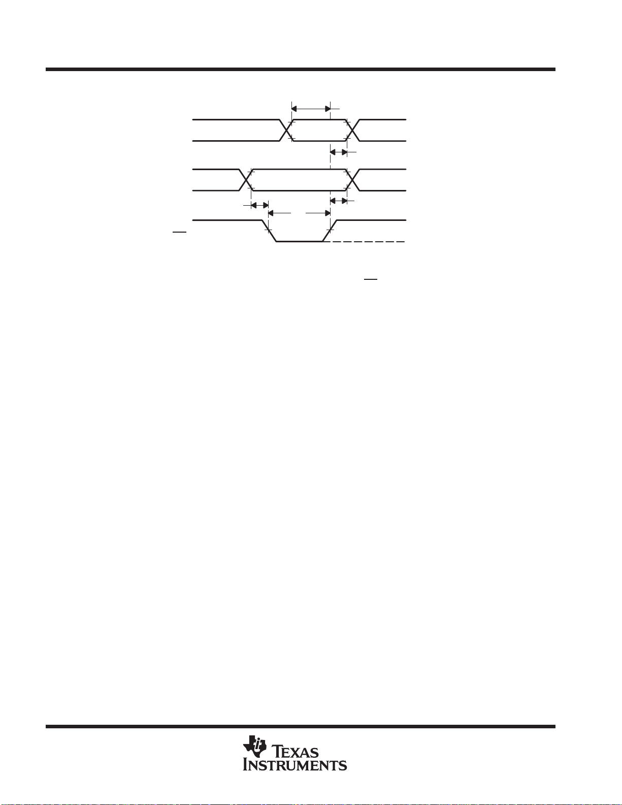
PARAMETER MEASUREMENT INFORMATION
t
su(DW)
Data
Address
t
su(AW)
WR
NOTES: A. tr = tf = 20 ns over VDD range.
B. The timing measurement reference level is equal to VIH + V
divided by 2.
C. The selected input latch is transparent while WR
data during this time can cause erroneous outputs.
Figure 1. Write-Cycle Voltage Waveforms
t
w
t
h(DW)
t
h(AW)
is low. Invalid
V
0 V
V
0 V
V
0 V
DD
DD
DD
IL
6
POST OFFICE BOX 655303 • DALLAS, TEXAS 75265

TLC7226C, TLC7226E
QUADRUPLE 8-BIT DIGITAL-TO-ANALOG CONVERTERS
SLAS060B – JANUARY 1995 – REVISED AUGUST 1996
TYPICAL CHARACTERISTICS
OUTPUT CURRENT
vs
OUTPUT VOLTAGE
200
150
100
50
–0.1
– Output Current – mA
O
I
–0.2
–0.3
–0.4
Source Current
Short-Circuit
Limiting
0
TA = 25°C
VSS = –5 V
Digital In = 0 V
–2 –1 0 1 2
VO – Output Voltage – V
VDD = 15 V
Sinking
Current Source
Figure 2
OUTPUT CURRENT (SINK)
OUTPUT VOLTAGE
700
TA = 25°C
VDD = 15 V
600
Aµ
500
VSS = –5 V
400
300
200
– Output Current (Sink) –
O
I
100
VSS = 0
0
0123456
VO – Output Voltage – V
Figure 3
vs
78910
POST OFFICE BOX 655303 • DALLAS, TEXAS 75265
7

TLC7226C, TLC7226E
QUADRUPLE 8-BIT DIGITAL-TO-ANALOG CONVERTERS
SLAS060B – JANUARY 1995 – REVISED AUGUST 1996
PRINCIPLES OF OPERATION
AGND bias for direct bipolar output operation
The TLC7226 can be used in bipolar operation without adding more external operational amplifiers as shown
in Figure 1 by biasing AGND to V
bipolar output with no additional components. The transfer values are shown in Table 1.
. This configuration provides an excellent method for providing a direct
SS
REF (V
4 18
= 5 V)
ref
TLC7226
VDD = 10 to 15 V
‡
AGND
‡
Digital inputs omitted for clarity.
DAC A
5
V
–5 V
_
+
63
SS
DGND
OUT
2
Output range
(5 V to –5 V)
Figure 4. AGND Bias for Direct Bipolar Operation
Table 1. Bipolar (Offset Binary) Code
DAC LATCH CONTENTS
LSBMSB
1111 1111
1000 0001
1000 0000
0111 1111
0000 0001
0000 0000
ANALOG OUTPUT
127
ǒ
ref
ǒ
ǒ
0 V
ǒ
ǒ
128
128
128
1
128
128
127
128
1
Ǔ
Ǔ
Ǔ
Ǔ
Ǔ
+*
)
)
*
*
–V
V
V
V
ref
ref
ref
V
ref
V
ref
AGND bias for positive output offset
The TLC7226 AGND terminal can be biased above or below the system ground terminal, DGND, to provide an
offset analog output voltage level. Figure 2 shows a circuit configuration to achieve this for channel A of the
TLC7226. The output voltage, V
VO+
V
BIAS
)
D
A
where DA is a fractional representation of the digital input word (0 ≤ D ≤ 255/256).
Increasing AGND above system GND reduces the output range. V
specified operation. Since the AGND terminal is common to all four DACs, this method biases up the output
voltages of all the DACs in the TLC7226. Supply voltages V
to DGND.
8
, at OUTA can be expressed as:
O
ǒ
Ǔ
V
I
POST OFFICE BOX 655303 • DALLAS, TEXAS 75265
– V
DD
and VSS for the TLC7226 should be referenced
DD
must be at least 4 V to ensure
ref
(1)

OPERATION
QUADRUPLE 8-BIT DIGITAL-TO-ANALOG CONVERTERS
PRINCIPLES OF OPERATION
AGND bias for positive output offset (continued)
TLC7226C, TLC7226E
SLAS060B – JANUARY 1995 – REVISED AUGUST 1996
4 18
V
I
AGND
5
V
bias
†
Digital inputs omitted for clarity.
DAC A
V
ref
TLC7226
V
†
_
+
SS
63
V
DGND
DD
2
OUTA
Figure 5. AGND Bias Circuit
interface logic information
Address lines A0 and A1 select which DAC accepts data from the input port. Table 2 shows the operations of
the four DACs. Figure 3 shows the input control logic. When the WR
selected DAC are transparent and the output responds to activity on the data bus. The data is latched into the
addressed DAC latch on the rising edge of WR
. While WR is high, the analog outputs remain at the value
corresponding to the data held in their respective latches.
Table 2. Function Table
signal is low, the input latches of the
CONTROL INPUTS
WR A1 A2
H
L
↑
L
↑
L
↑
L
↑
L = low, H = high, X = irrelevant
X
L
L
L
L
H
H
H
H
X
No operation
Device not selected
L
DAC A transparent
L
DAC A latched
H
DAC B transparent
H
DAC B latched
L
DAC C transparent
L
DAC C latched
H
DAC D transparent
H
DAC D latched
POST OFFICE BOX 655303 • DALLAS, TEXAS 75265
9

TLC7226C, TLC7226E
QUADRUPLE 8-BIT DIGITAL-TO-ANALOG CONVERTERS
SLAS060B – JANUARY 1995 – REVISED AUGUST 1996
PRINCIPLES OF OPERATION
interface logic information (continued)
17
A0
To Latch A
A1
WR
16
15
To Latch B
To Latch C
To Latch D
Figure 6. Input Control Logic
unipolar output operation
The unipolar output operation is the basic mode of operation for each channel of the TLC7226, with the output
voltages having the same positive polarity as V
(V
= AGND) or with positive/negative power supplies. The voltage at V
SS
to AGND to prevent parasitic transistor turn-on. Connections for the unipolar output operation are shown in
Figure 4. Transfer values are shown in Table 3.
. The TLC7226 can be operated with a single power supply
ref
must never be negative with respect
ref
10
POST OFFICE BOX 655303 • DALLAS, TEXAS 75265

PRINCIPLES OF OPERATION
unipolar output operation (continued)
TLC7226C, TLC7226E
QUADRUPLE 8-BIT DIGITAL-TO-ANALOG CONVERTERS
SLAS060B – JANUARY 1995 – REVISED AUGUST 1996
4
REF
NOTE A. 1 LSB
_
DAC A
DAC B
DAC C
DAC D
+
_
+
_
+
_
+
Figure 7. Unipolar Output Circuit
Table 3. Unipolar Code
DAC LATCH CONTENTS
LSBMSB
1111 1111
1000 0001
1000 0000
0111 1111
0000 0001
0000 0000 0 V
+ǒV
ref
ANALOG OUTPUT
ǒ
)
V
ref
ǒ
)
V
ref
ǒ
)
V
ref
ǒ
)
V
ref
ǒ
)
V
ref
–8
Ǔ
2
+
V
ref
255
256
129
256
128
256
127
256
1
256
ǒ
1
256
Ǔ
Ǔ
Ǔ
+)
Ǔ
Ǔ
2
OUTA
1
OUTB
20
OUTC
19
OUTD
V
ref
2
Ǔ
linearity, offset, and gain error using single-ended power supplies
When an amplifier is operated from a single power supply, the voltage offset can still be either positive or
negative. With a positive offset, the output voltage changes on the first code change. With a negative offset the
output voltage may not change with the first code depending on the magnitude of the offset voltage.
The output amplifier, with a negative voltage of fset, attempts to drive the output to a negative voltage. However,
because the most negative supply rail is ground, the output cannot be driven to a negative voltage.
So when the output offset voltage is negative, the output voltage remains at zero volts until the input code value
produces a sufficient output voltage to overcome the inherent negative offset voltage, resulting in a transfer
function shown in Figure 5.
POST OFFICE BOX 655303 • DALLAS, TEXAS 75265
11

TLC7226C, TLC7226E
QUADRUPLE 8-BIT DIGITAL-TO-ANALOG CONVERTERS
SLAS060B – JANUARY 1995 – REVISED AUGUST 1996
PRINCIPLES OF OPERATION
linearity, offset, and gain error using single-ended power supplies (continued)
Output
Voltage
0 V
Negative
Offset
DAC Code
Figure 8. Effect of Negative Offset (Single Power Supply)
This negative offset error, not the linearity error, produces the breakpoint. The transfer function would have
followed the dotted line if the output buffer could be driven to a negative voltage.
For a DAC, linearity is measured between zero input code (all inputs 0) and full scale code (all inputs 1) after
offset and full scale are adjusted out or accounted for in some way . However, single power supply operation does
not allow for adjustment when the offset is negative due to the breakpoint in the transfer function. So the linearity
in the unipolar mode is measured between full scale code and the lowest code which produces a positive output
voltage.
The code is calculated from the maximum specification for the negative offset.
12
POST OFFICE BOX 655303 • DALLAS, TEXAS 75265

TLC7226C, TLC7226E
QUADRUPLE 8-BIT DIGITAL-TO-ANALOG CONVERTERS
SLAS060B – JANUARY 1995 – REVISED AUGUST 1996
APPLICATION INFORMATION
bipolar output operation using external amplifier
Each of the DACs of the TLC7226 can also be individually configured to provide bipolar output operation, using
an external amplifier and two resistors per channel. Figure 9 shows a circuit used to implement offset binary
coding (bipolar operation) with DAC A of the TLC7226. In this case:
VO+1)
R2
ǒDA
R1
V
ref
R2
Ǔ
*
ǒV
R1
ref
Ǔ
with R1+R2
VO+
ǒ
2DA*
1Ǔ
V
ref
where DAis a fractional representation of the digital word in latch A.
Mismatch between R1 and R2 causes gain and offset errors. Therefore, these resistors must match and track
over temperature. The TLC7226 can be operated with a single power supply or from positive and negative
power supplies.
REF
†
4
DAC A
†
R1 = R2 = 10 kΩ ±0.1%
TLC7226
R1
_
+
2
R2
_
+
†
15 V
–15 V
V
O
Figure 9. Bipolar Output Circuit
staircase window comparator
(2)
In many test systems, it is important to be able to determine whether some parameter lies within defined limits.
The staircase window comparator shown in Figure 10 is a circuit that can be used to measure the V
OH
and V
OL
thresholds of a TTL device under test. Upper and lower limits on both VOH and VOL can be programmed using
the TLC7226. Each adjacent pair of comparators forms a window of programmable size (see Figure 1 1). When
the test voltage (V
) is within a window, then the output for that window is higher. With a reference of 2.56 V
test
applied to the REF input, the minimum window size is 10 mV.
POST OFFICE BOX 655303 • DALLAS, TEXAS 75265
13

TLC7226C, TLC7226E
QUADRUPLE 8-BIT DIGITAL-TO-ANALOG CONVERTERS
SLAS060B – JANUARY 1995 – REVISED AUGUST 1996
APPLICATION INFORMATION
staircase window comparator (continued)
V
test
From DUT
Reference Voltage
4
REF
OUTA
TLC7226
OUTB
OUTC
2
1
20
5 V
10 kΩ
+
_
Window 1
+
_
V
OH
V
OH
V
OL
+
_
+
_
+
_
+
_
+
_
+
_
5 V
10 kΩ
Window 2
5 V
10 kΩ
Window 3
5 V
10 kΩ
Window 4
5 V
V
OL
AGND
5
OUTD
19
+
_
+
_
Figure 10. Logic Level Measurement
10 kΩ
Window 5
14
POST OFFICE BOX 655303 • DALLAS, TEXAS 75265

TLC7226C, TLC7226E
QUADRUPLE 8-BIT DIGITAL-TO-ANALOG CONVERTERS
SLAS060B – JANUARY 1995 – REVISED AUGUST 1996
APPLICATION INFORMATION
staircase window comparator (continued)
REF
Window 1
OUTA
OUTB
OUTC
OUTD
AGND
Figure 11. Adjacent Window Structure
The circuit can easily be adapted as shown in Figure 12 to allow for overlapping of windows. When the three
outputs from this circuit are decoded, five different nonoverlapping programmable window possibilities can
again be defined (see Figure 13).
Reference Voltage
V
test
From DUT
4
REF
OUTA
Window 2
Window 3
Window 4
Window 5
2
5 V
10 kΩ
+
_
Window 1
+
_
5 V
OUTB
TLC7226
OUTC
OUTD
AGND
5
1
20
19
+
_
+
_
+
_
+
_
Figure 12. Overlapping Window Circuit
10 kΩ
Window 2
5 V
10 kΩ
Window 3
POST OFFICE BOX 655303 • DALLAS, TEXAS 75265
15

TLC7226C, TLC7226E
QUADRUPLE 8-BIT DIGITAL-TO-ANALOG CONVERTERS
SLAS060B – JANUARY 1995 – REVISED AUGUST 1996
APPLICATION INFORMATION
staircase window comparator (continued)
REF
OUTB
OUTA
OUTD
OUTC
AGND
Windows 1 and 2
Window 2
Windows 2 and 3
Window 1
Window 3
Figure 13. Overlapping Window Structure
output buffer amplifier
The unity-gain output amplifier is capable of sourcing 5 mA into a 2-kΩ load and can drive a 3300-pF capacitor.
The output can be shorted to AGND indefinitely or it can be shorted to any voltage between V
consistent with the maximum device power dissipation.
multiplying DAC
The TLC7226 can be used as a multiplying DAC when the reference signal is maintained between 2 V and
V
– 4 V . When this configuration is used, VDD should be 14.25 V to 15.75 V . A low output-impedance buffer
DD
should be used so that the input signal is not loaded by the resistor ladder. Figure 14 shows the general
schematic.
15 V
SS
and V
DD
AC Reference
Input Signal
R1
R2
_
+
15 V
OP07
V
ref
4
1/4 TLC7226
DAC
AGND DGND
56
Figure 14. AC Signal Input Scheme
_
V
+
O
16
POST OFFICE BOX 655303 • DALLAS, TEXAS 75265

TLC7226C, TLC7226E
QUADRUPLE 8-BIT DIGITAL-TO-ANALOG CONVERTERS
SLAS060B – JANUARY 1995 – REVISED AUGUST 1996
MECHANICAL DATA
DW (R-PDSO-G**) PLASTIC SMALL-OUTLINE PACKAGE
16 PIN SHOWN
16
0.050 (1,27)
0.020 (0,51)
0.014 (0,35)
1
A
0.010 (0,25)
9
8
M
0.419 (10,65)
0.400 (10,15)
0.299 (7,59)
0.293 (7,45)
PINS **
DIM
A MAX
A MIN
0.010 (0,25) NOM
0°–8°
16
0.410
(10,41)
0.400
(10,16)
Gage Plane
(12,95)
(12,70)
20
0.510
0.500
24
0.610
(15,49)
0.600
(15,24)
0.010 (0,25)
0.050 (1,27)
0.016 (0,40)
28
0.710
(18,03)
0.700
(17,78)
0.104 (2,65) MAX
NOTES: A. All linear dimensions are in inches (millimeters).
B. This drawing is subject to change without notice.
C. Body dimensions do not include mold flash or protrusion not to exceed 0.006 (0,15).
D. Falls within JEDEC MS-013
0.012 (0,30)
0.004 (0,10)
Seating Plane
0.004 (0,10)
4040000/B 03/95
POST OFFICE BOX 655303 • DALLAS, TEXAS 75265
17

TLC7226C, TLC7226E
QUADRUPLE 8-BIT DIGITAL-TO-ANALOG CONVERTERS
SLAS060B – JANUARY 1995 – REVISED AUGUST 1996
MECHANICAL DATA
N (R-PDIP-T**) PLASTIC DUAL-IN-LINE PACKAGE
16 PIN SHOWN
16
1
0.035 (0,89) MAX
PINS **
DIM
A
9
0.260 (6,60)
0.240 (6,10)
8
0.070 (1,78) MAX
0.020 (0,51) MIN
0.200 (5,08) MAX
A MAX
A MIN
Seating Plane
14
0.775
(19,69)
0.745
(18,92)
16
0.775
(19,69)
0.745
(18,92)
18
0.920
(23.37)
0.850
(21.59)
20
0.975
(24,77)
0.940
(23,88)
0.310 (7,87)
0.290 (7,37)
0.100 (2,54)
0.021 (0,53)
0.015 (0,38)
NOTES: A. All linear dimensions are in inches (millimeters).
B. This drawing is subject to change without notice.
C. Falls within JEDEC MS-001 (20 pin package is shorter then MS-001)
0.010 (0,25)
M
0.125 (3,18) MIN
0°–15°
0.010 (0,25) NOM
14/18 PIN ONL Y
4040049/C 08/95
18
POST OFFICE BOX 655303 • DALLAS, TEXAS 75265

IMPORTANT NOTICE
T exas Instruments and its subsidiaries (TI) reserve the right to make changes to their products or to discontinue
any product or service without notice, and advise customers to obtain the latest version of relevant information
to verify, before placing orders, that information being relied on is current and complete. All products are sold
subject to the terms and conditions of sale supplied at the time of order acknowledgement, including those
pertaining to warranty, patent infringement, and limitation of liability.
TI warrants performance of its semiconductor products to the specifications applicable at the time of sale in
accordance with TI’s standard warranty. Testing and other quality control techniques are utilized to the extent
TI deems necessary to support this warranty . Specific testing of all parameters of each device is not necessarily
performed, except those mandated by government requirements.
CERT AIN APPLICATIONS USING SEMICONDUCTOR PRODUCTS MAY INVOLVE POTENTIAL RISKS OF
DEATH, PERSONAL INJURY, OR SEVERE PROPERTY OR ENVIRONMENTAL DAMAGE (“CRITICAL
APPLICATIONS”). TI SEMICONDUCTOR PRODUCTS ARE NOT DESIGNED, AUTHORIZED, OR
WARRANTED TO BE SUITABLE FOR USE IN LIFE-SUPPORT DEVICES OR SYSTEMS OR OTHER
CRITICAL APPLICA TIONS. INCLUSION OF TI PRODUCTS IN SUCH APPLICATIONS IS UNDERST OOD TO
BE FULLY AT THE CUSTOMER’S RISK.
In order to minimize risks associated with the customer’s applications, adequate design and operating
safeguards must be provided by the customer to minimize inherent or procedural hazards.
TI assumes no liability for applications assistance or customer product design. TI does not warrant or represent
that any license, either express or implied, is granted under any patent right, copyright, mask work right, or other
intellectual property right of TI covering or relating to any combination, machine, or process in which such
semiconductor products or services might be or are used. TI’s publication of information regarding any third
party’s products or services does not constitute TI’s approval, warranty or endorsement thereof.
Copyright 1998, Texas Instruments Incorporated
 Loading...