

Page 1

SLLS528 – MARCH 2002
FEATURES
0.2-mA to 40-mA (Constant-Current Sink)
D
Drive Capability x 12 Bits Output Count into
24-Pin HTSSOP Package
D 1024 Gray-Scale Display (PWM Control 1024
Steps) with Max 25-MHz Clock Frequency
D 3-Way Brightness Adjustment
– Plane Brightness Adjustment for 64 Steps
(40% to 100%)
– Frequency Division for 16 Steps
(6.3% to 100%)
– Dot Correction for 256 Steps (0% to 100%)
D DS–Link Data Input/Output (Data Rate Max
20 Mbps) with Packet Operation
D 5 Error Information Types and 2 Gray–Scale
Clock Modes
D 3.3-V V
and LVTTL Interface
CC
APPLICATION
Full- or Multi-Color LED Display
D
DESCRIPTION
The TLC5930 is a constant-current sink driver
with an adjustable current value, and 1024 gray
scale display that uses pulse width control. The
output current is 0.2 mA to 40 mA with 12 bits of
RGBx4. The maximum current value of the
constant-current output can be set by one external
resistor.
The TLC5930 includes three kinds of brightness
adjustment functions: one adjusts the plane
brightness between devices, changing the current
values of all outputs uniformly. The second adjusts
the frequency division to controls overall panel
brightness, and the third adjusts the dot correction
per LED, changing the current values of
independent output.
The TLC5930 also includes color–tone correction
function for correcting color per dot (pixel) and
OVM function for constant-current output
terminals used for LED failure detection.
Other features include the thermal error flag
(TEF). The active wire-check (AWC) to check the
communication between the controller and the
device. The LED leakage-detect (LKD) to detect
the reverse leakage on the LED. The GCLK error
flag (GEF) and the HSYNC error flag (HEF) by
monitoring the gray-scale clock count, and the
dual source gray-scale clock (DSG) function to
switch the gray-scale clock to the external input
clock or to switch the internally-generated clock.
PowerPAD is a trademark of Texas Instruments Incorporated.
www.ti.com
The TLC5930 requires three signals for standard
operation: data input and gray-scale clock. Only
three-signal line and 24-pin HTSSOP package
reduce board area and total cost.
Copyright 2002, Texas Instruments Incorporated
1
Page 2
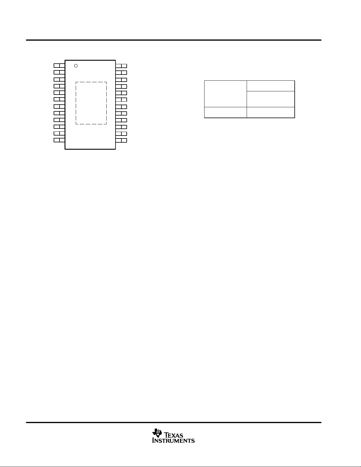
SLLS528 – MARCH 2002
PWP PACKAGE
(TOP VIEW)
OUT0
OUT1
OUT2
GND
OUT3
OUT4
OUT5
GND
DTIN
STIN
GCLK
GND
1
2
3
4
5
6
7
8
9
10
11
12
absolute maximum ratings over operating free-air temperature (unless otherwise noted)
24
23
22
21
20
19
18
17
16
15
14
13
OUT11
OUT10
OUT9
GND
OUT8
OUT7
OUT6
DTOUT
STOUT
XRST
IREF
VCC
AVAILABLE OPTIONS
T
A
–20°C to 85°C
PACKAGE
PowerPad TSSOP
(PWP)
TLC5930PWP
†
Supply voltage, VCC –0.3 V to 4.0 V. . . . . . . . . . . . . . . . . . . . . . . . . . . . . . . . . . . . . . . . . . . . . . . . . . . . . . .
Output current (dc), I
Input voltage range, V
Output voltage range, V
Storage temperature range, T
Power dissipation rating at (or above) T
†
Stresses beyond those listed under “absolute maximum ratings” may cause permanent damage to the device. These are stress ratings only, and
functional operation of the device at these or any other conditions beyond those indicated under “recommended operating conditions” is not
implied. Exposure to absolute-maximum-rated conditions for extended periods may affect device reliability.
NOTES: 1. All voltages values are with respsect to GND terminal.
2. At operating temperature range over 25°C, dependent on derating factor of 41 mW/°C.
O(LC)
IN
DTOUT
V
OUT0 –
V
OUT0 –
stg
, V
V
V
STOUT
, (when off) –0.3 V to 17 V. . . . . . . . . . . . . . . . . . . . . . . . . . . . . . . . . .
OUT11
, (when on) –0.3 V to 10 V. . . . . . . . . . . . . . . . . . . . . . . . . . . . . . . . . .
OUT11
= 25°C 3.7 W. . . . . . . . . . . . . . . . . . . . . . . . . . . . . . . . . . . . . . . . . . . . . .
A
–0.3 V to (VCC – 0.2 V). . . . . . . . . . . . . . . . . . . . . . . . . . . . . . . . . . . .
–0.3 V to VCC. . . . . . . . . . . . . . . . . . . . . . . . . . . . . . . . . . . . . . . . . . . . . . . . . . . . . . . .
–40°C to 125°C. . . . . . . . . . . . . . . . . . . . . . . . . . . . . . . . . . . . . . . . . . . . . . . . . . . .
45 mA. . . . . . . . . . . . . . . . . . . . . . . . . . . . . . . . . . . . . . . . . . . . . . . . . . . . . . . . . . . . .
2
www.ti.com
Page 3
Á
Á
Á
Á
Á
Á
Á
Á
Á
Á
Á
Á
Á
Á
Á
Á
Á
Á
Á
Á
Á
Á
t
Á
P
Á
Á
Á
Á
Á
Á
Á
Á
Á
Á
Á
SLLS528 – MARCH 2002
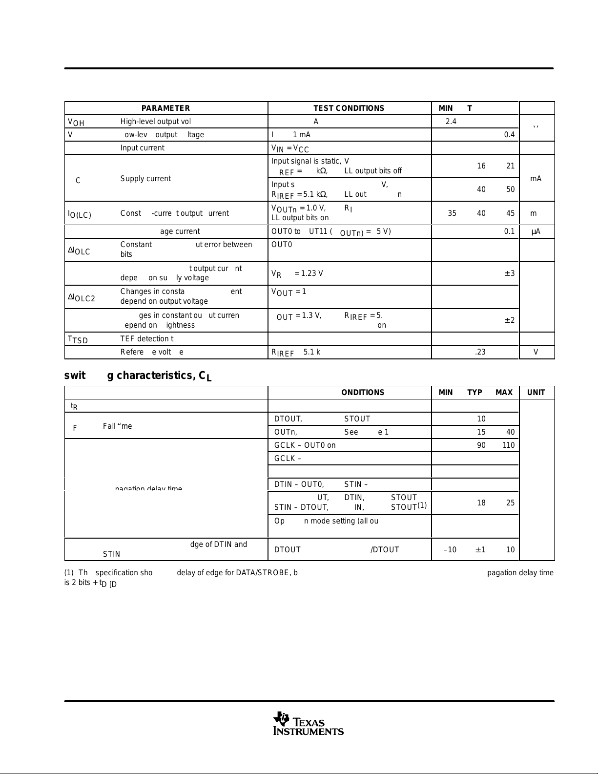
electrical characteristics, MIN/MAX: V
TA = 25°C (unless otherwise noted)
PARAMETER
V
OH
V
OL
I
I
I
CC
ÁÁ
I
O(LC)
I
LKG
∆I
OLC
ÁÁ
∆I
OLC1
∆I
ÁÁ
OLC2
∆I
OLC3
ÁÁ
T
TSD
V
IREF
High-level output voltage
Low-level output voltage
Input current
Supply current
БББББББББ
Constant-current output current
Output leakage current
Constant-current outout error between
БББББББББ
bits
Changes in constant output current
depend on supply voltage
Changes in constant output current
БББББББББ
depend on output voltage
Changes in constant output current
depend on brightness data
БББББББББ
TEF detection temperature
Reference voltage
= 3.0 V to 3.6 V, T
CC
= – 20°C to 85°C, TYP: V
A
TEST CONDITIONS
IOH = – 1 mA
IOL = 1 mA
VIN = VCC or GND
Input signal is static, V
R
= 5.1 kΩ, LL output bits off
IREF
Input signal is static, V
ББББББББББ
R
= 5.1 kΩ, LL output bits on
IREF
V
= 1.0 V, R
OUTn
LL output bits on
OUT0 to OUT11 (V
OUT0 to OUT11 (V
ББББББББББ
R
= 5.1 kΩ
IREF
V
= 1.23 V
REF
V
= 1 V to 3 V, R
OUT
ББББББББББ
V
= 1.23 V, 1 bit light on
IREF
V
= 1.3 V, R
OUT
V
= 1.23 V, 1 bit light on
IREF
ББББББББББ
OUT
OUT
IREF
(OUTn)
(OUTn)
IREF
IREF
= 1 V,
= 1 V,
= 5.1 kΩ,
= 15 V)
= 1 V),
= 5.1 kΩ,
= 5.1 kΩ,
Junction temperature
R
= 5.1 kΩ
IREF
CC
MIN
TYP
MAX
2.4
16
35
40
40
160
1.23
Á
± 4%
170
ÁÁÁ
ÁÁÁÁÁ
ÁÁÁÁÁ
ÁÁÁÁÁ
150
= 3.3 V,
0.4
± 1
21
50
45
0.1
± 3
± 1
± 2
UNIT
µA
mA
Á
mA
µA
Á
%/V
Á
Á
°C
V
V
switching characteristics, CL = 15 pF
PARAMETER
t
R
t
F
Rise time
Fall time
DTOUT, STOUT
DTOUT, STOUT
OUTn, See Figure 1
GCLK – OUT0 on
GCLK – OUT0 off
[(OUTn + 1) – OUTn]
PD
Á
p
ropagation delay time
ББББББББББ
DTIN – OUT0, STIN – OUT0
DTIN – DTOUT, DTIN, STOUT
ББББББББББ
STIN – DTOUT, STIN, STOUT
Operation mode setting (all output force off)
– OUT0 off
t
EDGE
Duty deviation between edge of DTIN and
Á
ББББББББББ
STIN
DTOUT/STOUT, STOUT/DTOUT
ББББББББББ
(1) This specification shows the delay of edge for DATA/STROBE, but data appears in the output with 2 bits delay. (Data propagation delay time
is 2 bits + tD
[D/STIN – D/STOUT]
)
TEST CONDITIONS
(1)
ÁÁÁ
Á
MIN
–10
TYP
Á
12
10
15
90
35
25
18
60
± 1
MAX
110
Á
Á
15
13
40
60
40
60
25
90
10
UNIT
ns
Á
Á
www.ti.com
3
Page 4

V
mA
SLLS528 – MARCH 2002
recommended operating conditions
dc characteristics
PARAMETER
Supply voltage, V
Voltage applied to constant-current output, V
High-level input voltage, V
Low-level input voltage, V
High-level output current, I
Low-level output current, I
Constant output current, I
Operating free-air temperature range, T
CC
O
IH
IL
OH
OL
O(LC)
A
CONDITIONS
OUT0 to OUT11 off
OUT0 to OUT11 on
VCC = 3.1 V @ DTOUT, STOUT
VCC = 3.1 V @ DTOUT, STOUT
OUT0 to OUT11
MIN
GND
3.0
2.0
– 20
MAX
VCC
– 1.0
3.6
15
10
0.8
1.0
40
85
UNIT
V
mA
°C
ac characteristics, V
PARAMETER
f
(GCLK)
t
(EDGE)
t
w(H)/tw(L)
t
w(L)
t
(DATA)
t
SU
(1) This is the frequency when any output is obtailed at two or more than gray-scale entered.
GCLK clock frequency
Time between edges
GCLK pulse duration
XRST reset pulse duration
Data transfer rate
Setup time
= 3.1 V to 3.5 V, T
CC
(1)
= –20°C to 85°C (unless otherwise noted)
A
CONDITIONS
2 gray scale inputs I
DTIN – STIN, STIN – DTIN
HSYNC – GCLK
O(LC)
= 40 mA
MIN
30
20
MAX
1
25
20
6.5
UNIT
MHz
ns
ms
Mb/s
ns
4
www.ti.com
Page 5
functional block diagram
SLLS528 – MARCH 2002
VCC
DTIN
STIN
GCLK
XRST
330 kΩ
D/S
Link
Decoder
CLR
Communication Logic
CLK
Packet
Interface
BLANK, FON, FOF, INHSW, INHCS
Packet
Shift
Register
GSCLK
Packet
Data
Latch
GS, BCP
PWM
Controller
Packet
Interface
DMDATA
D/S
Link
Decoder
DTOUT
STOUT
IREF
GND
Bandgap
Reference
Generator
BG, IBC
BG
Reference
Voltage
&
Bias Current
Generator
GND = DGND, AGND, LGND
ITEF
IOVM
BC
IDC,ICC
Analog Converter
Trimming
Circuit
Digital to Analog Converter
12-Bit Constant Current Driver
OUT2
OUT1
OUT0
OUT4
OUT3
&
OUT5
DC, CC
OUT6
OUT7
OUT9
OUT8
SW, CSW
OUT11
OUT10
Thermal
Error
Flag
Output
Voltage
Monitor
&
LED Leak
Detector
www.ti.com
5
Page 6
SLLS528 – MARCH 2002
Terminal Functions
TERMINAL
NAME NO.
DTIN 9 I DS–link data input
DTOUT 17 O DS–link data output
GCLK 11 I
GND 4, 8, 12, 21 – Ground
IREF 14 I/O
OUT0 1
OUT1 2
OUT2 3
OUT3 5
OUT4 6
OUT5 7
OUT6 18
OUT7 19
OUT8 20
OUT9 22
OUT10 23
OUT11 24
STIN 10 I DS–link strobe input
STOUT 16 O DS–link strobe output
VCC 13 I Power supply
XRST 15 I
I/O
Clock input for gray scale. The gray scale display is accomplished by lighting the LED until the
number of the gray-scale clock counted is equal to the data latched.
Constant-current value setting. LED current is set to the desired value by connecting an external
resistor between IREF and GND. The 168 times current compared to current across the external
resistor flows through the constant-current output terminals.
Constant-current output.
O
Reset signal. This signal is used to initialize the device reset is accomplished by pulling this pin low
(internally pulled up with a 330-kΩ resistor). If not used, this terminal should be left open or connect
to VCC.
DESCRIPTION
6
www.ti.com
Page 7
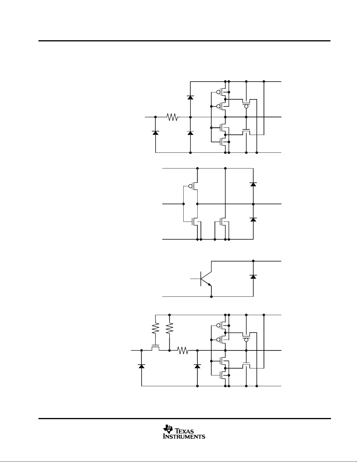
PIN EQUIVALENT INPUT AND OUTPUT SCHEMA TIC DIAGRAMS
DTIN, STIN, GCLK
PAD
SLLS528 – MARCH 2002
VCC
DTOUT, STOUT
OUTn
XRST
GND
VCC
PAD
GND
PAD
GND
VCC
PAD
330 k
www.ti.com
GND
7
Page 8
SLLS528 – MARCH 2002
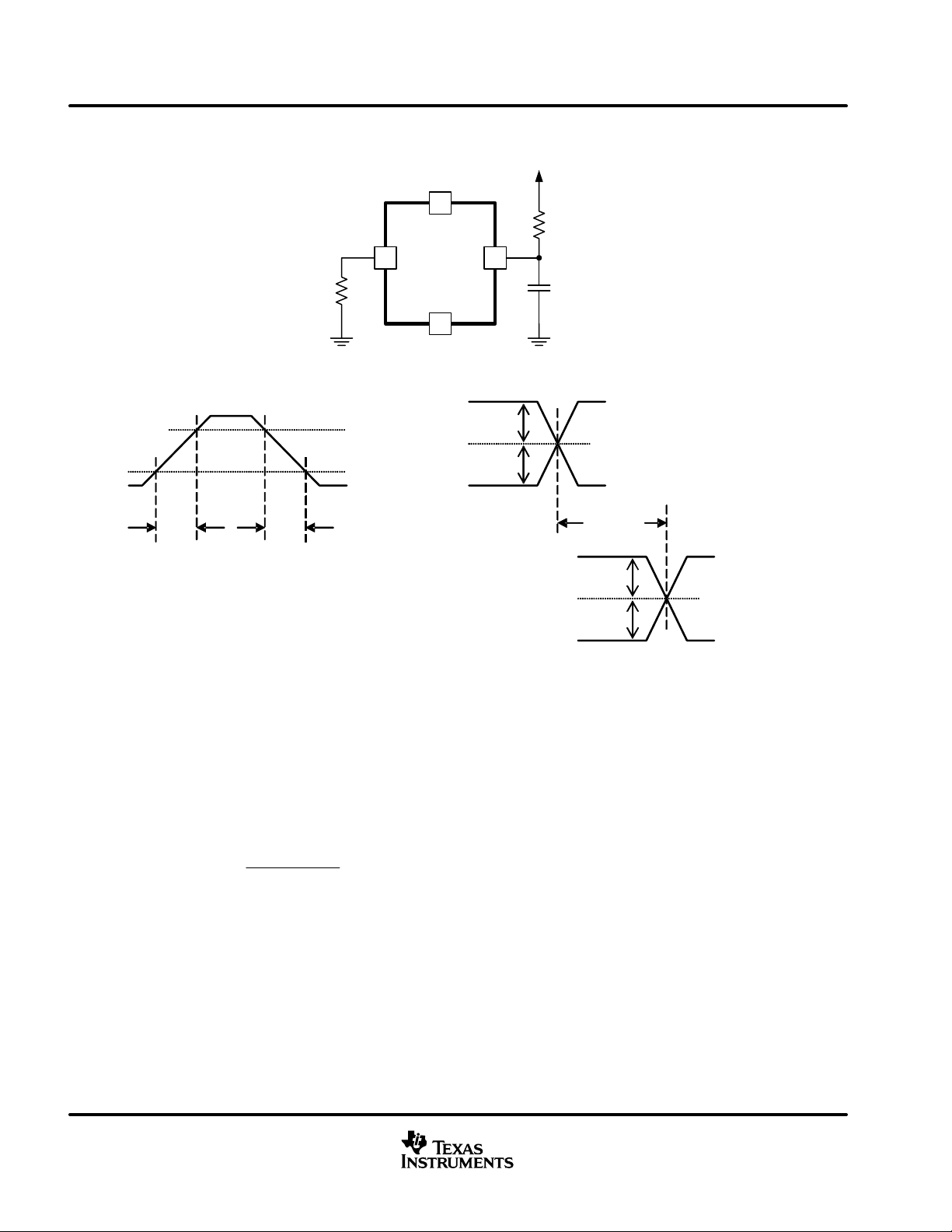
TIMING DIAGRAMS
VCC
VIL
Figure 1. Rise Time and Fall Time Test Circuit for OUTn
VIH
tR tF
5.1 kΩ
90%
10%
VCC
IREF OUTn
GND
56 Ω
15 pF
VIH or VOH
50%
50%
VIL or VOL
txxxx
VIH or VOH
50%
50%
VIL or VOL
Figure 2. Timing Requirements
PRINCIPLES OF OPERATION
setting for constant output current value
On the constanct current output terminals (OUT0 to OUT11), approximately 168 times the current that flows
through the external resistor, R
is calculated using the following equation:
R
where R
(IREF)
(IREF)
(W) +
168 1.23 V
I
O(LC)
should be ≤ 4.88 kΩ
Note that more current flows if IREF is connected directly to GND.
, (connected between IREF and GND) can flow. The external resistor value
IREF
(A)
(1)
8
www.ti.com
Page 9
NO. OF
NO. OF
SLLS528 – MARCH 2002
PRINCIPLES OF OPERATION
command packet list
ID COMMAND
FUNCTION
Internal reset 00 X 00 00000000 8(03h) 24 Write
Gray scale data setting 00or01.FF X X 02 00000010 10x12 output 136 Write
Dot correction data setting 00or01.FF X X 04 00000100 8x12 output 112 Write
Color tone correction data setting 00or01.FF X X 08 00001000 8x4set 48 Write
Plane brightness adjustment data setting 00or01.FF X X 10 00010000 16 32 Write
Color tone correction control setting 00or01.FF X X 20 00100000 8 24 Write
Operation mode setting 00or01.FF X X 40 01000000 16 32 Write
OVM information read 00or01.FF X X 50 01010000 16 32 Read
Failure monitor information read 00or01.FF X X 60 01100000 8 24 Read
Automatical ID setting 00 X 70 01110000 16(min) 32(min) Write
HSYNC synchronization 00 X 80 10000000 16 32 Wr/Rd
NOTE Common control is applied to all the devices connected. Indidual control is applied to the device specified by ID.
HEX
CONTROL
COMMON INDIVIDUAL
HEX BIN
DATA
BITS BITS
PACKET MODE
basic packet configuration
MSB LSB
ID (8 bit)
MSB
data configuration
DATA
GCLK
LSB
CMD (8 bit)
MSB
LSB
DATA (0 to 120 bit)
MSB
DQ
Q
DQ
Q
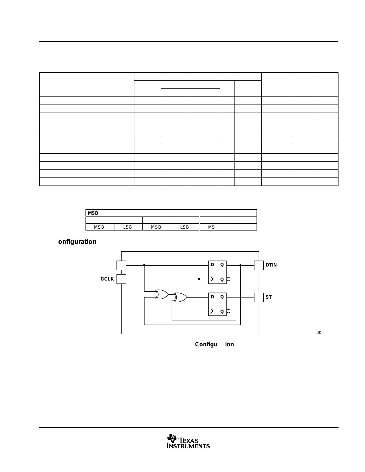
Figure 3. DS LINK Configuration
LSB
DTIN
STIN
UDG–02058
www.ti.com
9
Page 10
SLLS528 – MARCH 2002
PRINCIPLES OF OPERATION
packet operation
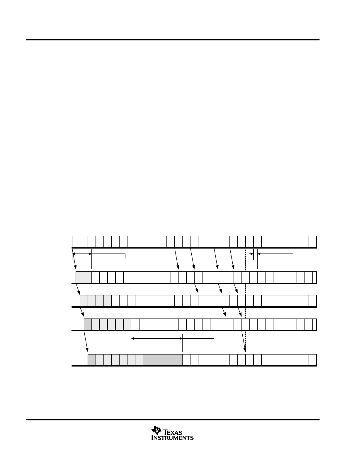
Data output is performed with delay of two bits from input. In other words, by using the edge of the input, data
before two b i t s appear in the output terminal. Figure 4 shows the concept for data transfer when some TLC5930s
are connected in a cascade, where data A–Z indicates valid data, and the asterisk (*) marks invalid data. Also,
data A is a first data input from controller, and there is assumed to be no data transition for DATA/STROBE
between [H and I] and [S and T] in the IC1 input data.
Invalid data is clocked out corresponding to the input edge to ensure that no data exists before data A. After
that, data A is clocked out with a time delay of two bits plus t
D(D/STIN–D/STOUT)
Once data output is started, data before two bits from current input is sequentially clocked out using the input
edge. It should be noted that data output stays during no transition of DATA/STROBE, since no input edge
makes the out p u t edge. Figure 4 shows that the output of IC1 remains in data F and does not go to data G until
the edge of input data I is entered (after IC1 clocked out data F , although the input data of IC1 is continued from
A to H.)
If data A to H are included in one packet, the data output for each output of the device in data H, (which indicates
the completion of packet operation), is performed out at the edge establishing data J for IC1, data L for IC2, data
O for IC3, and data Q for IC4 from the view of controller. In other words, in order to complete the packet operation
for all the devices connected in cascades, additional bit data equivalent to two times the number of devices
cascaded is needed to be clocked in.
using the input edge for data C.
Additionally , s i n c e e a c h d evice has the time delay, T
D(D/STIN–D/STOUT)
, from input to output, the controller views
that output having a time delay exceeding two bits against a virtual input to IC1. In this example, while, in
practice, the output data H for IC4 is established by the input edge of data Q, it appears to be synchronized with
data S for IC1.
A B C D E F G H I J K L M O P Q R S T U V W X Y Z
IC1 INPUT DATA
t
D(D/STIN–D/STOUT)
M O P Q R SI J K LGC DA B
M O P QI J K LGC DA B F
IC2 INPUT DATA
IC1 OUTPUT DATA
IC3 INPUT DATA
IC2 OUTPUT DATA
IC4 INPUT DATA
IC3 OUTPUT DATA
IC4 OUTPUT DATA
2 bit+t
D(D/STIN–D/STOUT)
A B C D E G H F I J L MK O P Q R S T U V W X
**
* * **
* * **
* * **
A B C D E G H F I J L MK O P Q R S T U V
F
**
* *
**
E
2-bit + tD
(D/STIN – D/STOUT)
H
E
H
UDG–02032
10
Figure 4. Data Transfer Concept in Cascade Connection
www.ti.com
Page 11

SLLS528 – MARCH 2002
PRINCIPLES OF OPERATION
As shown in Figure 4, in order for all the cascade-connected devices to complete one packet operation,
additional bit data to input to the first stage equivalent to two times the number of devices cascaded is required
to be clocked in. But, in practice, sending just any data is not acceptable, and some packets with bits
corresponding to two times the number of devices connected are needed for synchronization to be successful.
For example, in the case that 16 ICs are connected in cascade, since 16 x 2 = 32 bits are needed to complete
the packet operation of sixteenth IC, OVM information reading packet as a dummy, which does not write any
data to the device, is desirable. Or, an alternative method to send any packet such as use of unused ID (e.g.
FFh) is available.
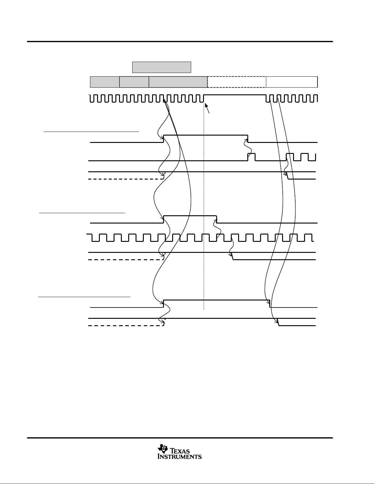
Figure 5 shows the concept for normal lighting-ON operation (based on pulse-width control method). Internal
BLANK goes high on the falling edge of the 21st bit in the HSYNC packet. If the constant-current output is ON
at that time, it is turned off (except for force on mode), and the data for which the latch flag is set in the HSYNC
packet is la t ched during internal BLANK high-level. Internal BLANK goes low on the rising edge of the gray-scale
clock (GCLK) after the edge of LSB (32nd bit) for HSYNC packet, and the TLC5930 goes into the status that
can be turned on by the constant-current output. The constant-current output is turned on by the next rising edge
of the gray-scale clock.
During power up, the initial value of BLANK is at a high level, therefore, operation for BLANK and
constant-current output when HSYNC packet is entered for the first time as a normal operation is dif ferent from
the example shown in Figure 5.
In addition, since BLANK and the gray-scale clock are ignored in the force-ON mode, the timing to be lighted
on is also different from the example shown in Figure 5.
www.ti.com
11
Page 12
SLLS528 – MARCH 2002
PRINCIPLES OF OPERATION
HSYNC packet
DATA INPUT
1
INTERNAL CLOCK
When Gray Scale Clock is Not Sequential
INTERNAL BLANK
GCLK
CONSTANT
CURRENT OUTPUT
When Gray Scale Clock Is Sequential
INTERNAL BLANK
GCLK
CONSTANT
CURRENT OUTPUT
10
20
DATA
Next PacketID CMD
30
LSB of HSYNC Packet
Light ON
Light ON
When Internal Gray Scale Clock Is Used
INTERNAL BLANK
CONSTANT
CURRENT OUTPUT
12
Light ON
Figure 5. Normal Lighting-ON Operation
www.ti.com
Page 13

SLLS528 – MARCH 2002
PRINCIPLES OF OPERATION
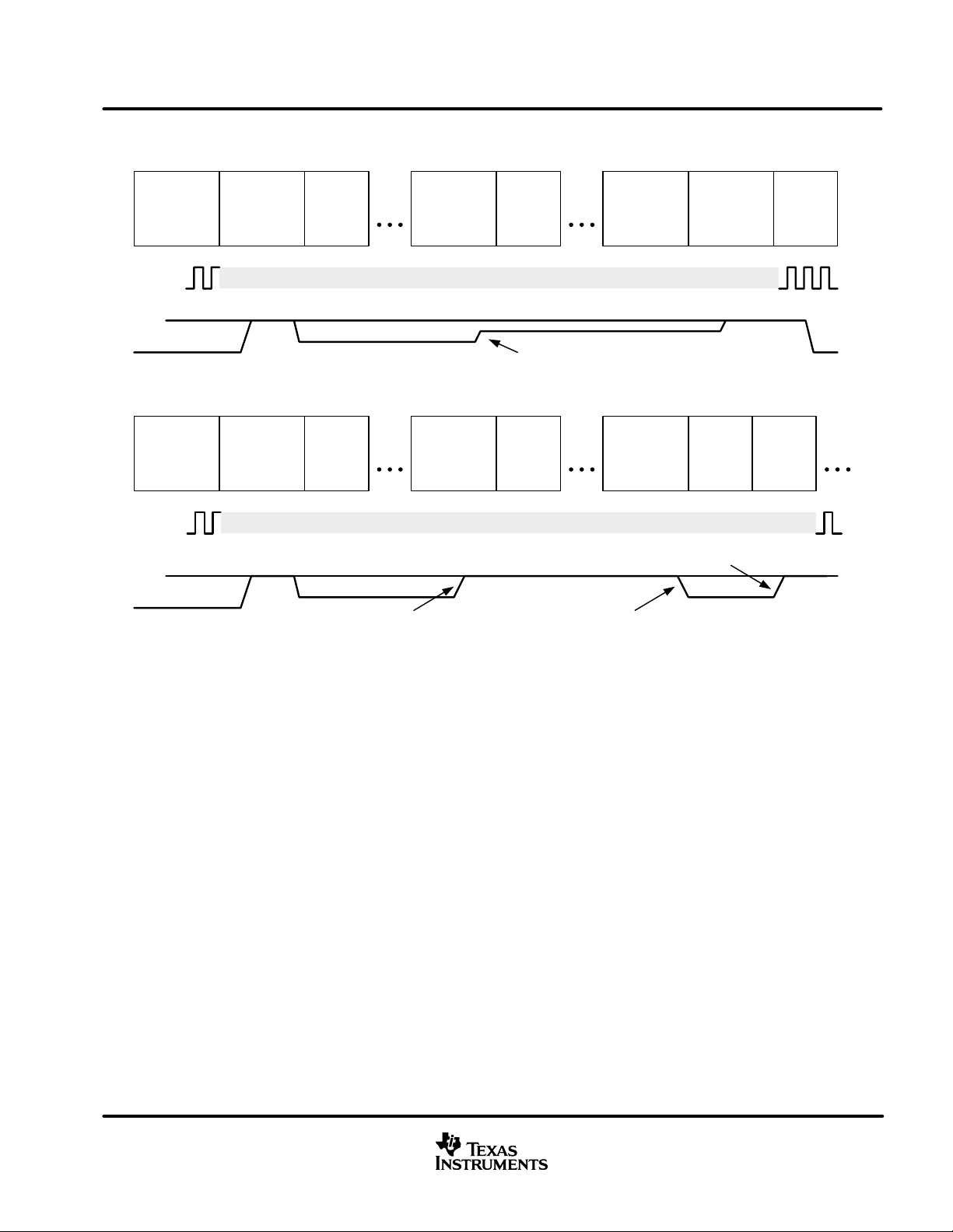
There are two different methods available as shown in Figure 6 for entering the gray-scale clock when in
light-ON mode. When the gray-scale clock is sequential, lighting-ON by the device is initiated after the HSYNC
packet operation for each device has been completed. When the external clock is used as gray-scale clock, all
the devices can be lighted-ON simultaneously by entering the gray scale clock after the HSYNC packet is
entered for the last device (in this example, just after OVM information reading packet has entered to IC1).
When Light-ON in a 4 Gray Scale With 16 ICs
When Gray Scale Clock Is Sequential (Including Use of Internally Generated Gray-Scale Clock)
GRAY SCALE
CLOCK
IC1 D/STIN
IC2 D/STIN
IC15 D/STIN
IC16 D/STIN
When Gray Scale Clock Is Not Sequential (External Input Only)
GRAY SCALE
CLOCK
IC1 D/STIN
HSYNC Packet 32 bits
IC1 Constant Current Output
HSYNC Packet 32 bits
IC2 Constant Current Output
Other Packet
IC15 Constant Current Output
Other Packet
IC16 Constant Current Output
HSYNC Packet 32 bits
IC1 Constant Current Output
OVM Information Reading Packet 32bits
OVM Information Reading Packet 32bits
ON
OVM Information Reading Packet 32bits
ON
HSYNC Packet 32 bits
ON
HSYNC Packet 32 bits
ON
ON
IC2 D/STIN
IC15 D/STIN
IC16 D/STIN
HSYNC Packet 32 bits
IC2 Constant Current Output
Other Packet
IC15 Constant Current Output
Other Packet
IC16 Constant Current Output
Figure 6. Lighting-ON Operation With 16 Devices
OVM Information Reading Packet 32bits
HSYNC Packet 32 bits
HSYNC Packet 32 bits
www.ti.com
ON
ON
ON
13
Page 14

SLLS528 – MARCH 2002
PRINCIPLES OF OPERATION
command packet and operation
internal reset
By sending this packet once, the internal register within all the devices connected is set to the default value and
synchronized with the controller. Note that individual reset for the device is not available.
packet configuration
ID (bin)
00000000
default value
REGISTER DEFAULT VALUE COMMENTS
ID xxxxxxxx Indeterminate (no write) Automatic ID setting
Plane brightness 111111 (bin) 100%
Frequency division ratio 0000 (bin) 1/1 (no frequency division)
Dot correction 11111111 (bin) × 12 (output) 100% Dot correction data setting
Color tone correction 00000000 (bin) × 4 0% Color tone correction setting
Gray scale 0000000000 (bin) × 12 (output) 0 Gray scale data setting
CCEN–2
(color tone correction ON/OFF)
FORCE OFF 0 Normal operation Operation mode setting
FORCE ON 0 Normal operation Operation mode setting
DCEN 0 Dot correction disable Operation mode setting
BCEN 0 Brightness control disable Operation mode setting
LKDEN 0 LKD disable Operation mode setting
DSGSL 0 Use GCLK terminal Operation mode setting
OVM comparator voltage 0000 (bin) 0.3 V Operation mode setting
OVMF, OVMFA, GEF, HEF,
TEF
000 (bin) Color tone correction disable Color tone correction control
1
CMD (bin)
00000000
CMD (bin)
00000011
Plane brightness adjustment
data setting
Plane brightness correction
data setting
HSYNC, fault information
reading
initialization
During power up, the device is in an indeterminate condition. To fully reset the device after power up, it is
necessary to send an internal reset packet after entering the reset pulse to the XRST terminal or after sending
a 0 to each device 256 times as a dummy and then 03h.
Table 1. Input Configuration After Power-Up When Using XRST (reset pulse + 24 bit)
XRST
RESET (NEGATIVE PULSE)
(03000003h)
Note: Both DTIN and STIN should be 0 during XRST 0.
INTERNAL RESET PACKET
00000000
00000000
00000011
Table 2. Input Configuration After Power-Up When Not Using XRST (256 bit × devices + 24 bit)
14
DUMMY (bin)
0 (256 × devices)
(00h [256 bits × n] + 03000003h)
DATA (bin)
00000011
00000000
www.ti.com
INTERNAL RESET PACKET
00000000
00000011
Page 15

CMD
ÁÁÁ
ÁÁÁ
ÁÁÁ
ÁÁÁ
ÁÁÁ
ÁÁÁ
ÁÁÁ
ÁÁÁ
Á
Á
ÁÁÁ
Á
Á
Á
Á
ÁÁÁ
Á
Á
Á
Á
ÁÁÁ
Á
Á
Á
Á
ÁÁÁ
ÁÁÁ
ÁÁÁ
Á
ÁÁÁ
ÁÁÁ
ÁÁÁ
ÁÁÁ
ÁÁÁ
ÁÁÁ
SLLS528 – MARCH 2002
PRINCIPLES OF OPERATION
gray scale data
Using this packet, the same gray-scale data can be written to all the connected devices simultaneously or
different gray-scale data can be written to each device.
The constant-current output is turned on (constant-current flows), except that gray-scale data entered to
gray-scale data latch is 0, synchronizing with the next rising edge of the gray-scale clock after the rising edge
of the gray-scale clock with the time delay of t
the 10-bit gray-scale counter counts the number of rising edge of the gray-scale clock and outputs is matched
to gray-scale data is turned off (constant-current flow stops).
The user can select either the gray scale clock using GCLK terminal input or the internally generated clock using
DTIN/STIN terminal input. (See DSG function section for more detail)
Table 3. Packet Configuration (136-bit)
from the edge of DTIN/STIN of HSYNC packet LSB. Thereafter ,
su
ID
(bin)
xxxxxxxx
CMD
(bin)
00000010
DATA
OUT0
10 bit
OUT1
10 bit
OUT2
10 bit
OUT3
10 bit
OUT4
10 bit
OUT5
10 bit
OUT6
10 bit
OUT7
10 bit
OUT8
10 bit
OUT9
10 bit
OUT10
10 bit
OUTn
dt [9]
Á
ББББББББББББББББББББББÁÁÁÁÁ
dt [8]
ÁÁ
0
0
1
1
dt [7]
0
0
1
1
Á
0
0
1
1
dt [6]
Á
dt [5]
ÁÁ
0
0
1
1
0
0
1
1
dt [4]
Á
0
0
1
1
dt [3]
Á
dt [2]
ÁÁ
0
0
1
1
0
0
1
1
dt [1]
Á
0
0
1
1
dt [0]
Á
0
1
0
1
GRAY SCALE
DATA
ÁÁÁÁ
0
1
.
.
.
1023
1024
(xx02xxxxxxxxxxxxxxxxxxxxxxxxxxxxxxxxh) After ID and CMD, 10 bit data continues 12 output
OUT11
10 bit
www.ti.com
15
Page 16
CMD
ÁÁÁ
ÁÁÁ
Á
Á
Á
Á
Á
Á
ÁÁÁ
Á
Á
Á
Á
Á
ÁÁÁ
ÁÁÁ
Á
Á
ÁÁÁ
SLLS528 – MARCH 2002
PRINCIPLES OF OPERATION
dot correction data
Using this packet, the same dot correction data can be written to all connected devices simultaneously, or
different dot correction data can be written to each device.
The dot correction register latch is configured with 12 output x 8 bit; the current value on each constant output
current can be adjusted in 256 steps as 1 step of 0.4% of current ratio between 100% and 0% when output
current is set to 100% by adjusting external resistor and brightness adjustment data. By using this function,
brightness deviation due to brightness variation of LED can be reduced.
Table 4. Packet Configuration (112-bit)
OUT5
8 bit
DATA
OUT6
8 bit
OUT7
8 bit
OUT8
8 bit
OUT9
8 bit
ID
(bin)
xxxxxxxx
CMD
(bin)
00000100
OUT0
8 bit
OUT1
8 bit
OUT2
8 bit
OUT3
8 bit
OUT4
8 bit
OUTn
RELATIVE
dt [7]
ÁÁ
0
0
dt [6]
Á
dt [5]
Á
0
0
0
0
dt [4]
ÁÁ
0
0
dt [3]
Á
0
0
dt [2]
ÁÁ
0
0
dt [1]
Á
dt [0]
Á
0
0
0
1
CURRENT
ÁÁÁÁ
RATIO (%)
0.0
0.4
.
.
ББББББББББББББББББÁÁÁÁÁ
1
1
1
1
1
1
1
1
1
1
1
1
1
1
0
1
.
99.6
100
(xx04xxxxxxxxxxxxxxxxxxxxxxx xh) After ID and CMD, 8 bit data continues 12 output.
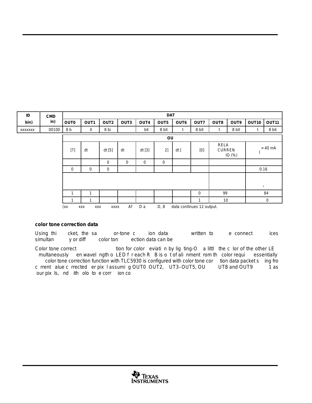
color tone correction data
Using this packet, the same color-tone correction data can be written to all the connected devices
simultanoeously or different color tone correction data can be written to each device.
Color tone correction makes correction for color deviation by lighting-ON a little the color of the other LED
simultaneously when wavelength of LED for each RGB is out of alignment from the color required essentially.
The color tone correction function with TLC5930 is configured with color tone correction data packet setting fro
current value corrected per pixel assuming OUT0–OUT2, OUT3–OUT5, OUT6–OUT8 and OUT9–OUT11 as
four pixels, and with color tone correction control packet which controls ON/OFF by OUT0, OUT3, OUT6, OUT9,
and OUT1, OUT4, OUT7, OUT10, and OUT2, OUT5, OUT8, and OUT11 assuming that same color is assigned
for OUT0, OUT3, OUT6, OUT9 and OUT1, OUT4, OUT7, OUT10 and OUT2, OUT5, OUT8, and OUT11
respectively.
OUT10
8 bit
I
ÁÁÁÁ
OLC
OUT11
8 bit
= 40 mA
(mA)
0.0
0.16
.
.
.
ÁÁÁÁ
39.84
40.00
The current value for color tone correction set by this packet is set per pixel for OUT0–OUT2, OUT3–OUT5,
OUT6–OUT8, and OUT9–OUT11. In other words, the current value for color tone correction is same in
OUT0–OUT2, OUT3–OUT5, OUT6–OUT8, and OUT9–OUT11.
16
www.ti.com
Page 17

Á
БББББББББББББББ
Á
Á
ÁÁÁ
ÁÁÁ
БББББ
Á
Á
ÁÁÁ
Á
Á
Á
Á
ÁÁÁ
Á
Á
Á
Á
БББББ
Á
Á
Á
ÁÁÁ
ÁÁÁ
БББББ
ÁÁÁ
ÁÁÁ
БББББ
Á
Á
БББББББББББББББ
Á
Á
БББББ
Á
Á
Á
ÁÁÁ
ÁÁÁ
БББББ
ÁÁÁ
ÁÁÁ
БББББ
ÁÁÁ
БББББББББББББББ
БББББББББББББББ
БББББББББББББББ
БББББББББББББББ
БББББББББББББББ
SLLS528 – MARCH 2002
PRINCIPLES OF OPERATION
The color tone correction register latch is configured with a 4 pixel × 8 bit, and the current value for color tone
correction by pixel can be adjusted between 50% and 0% when output current is set to 100% by adjusting
external resistor and brightness adjustment data. The color tone correction is divided into the coarse adjustment
with 2 bit / 4 steps and the fine adjustment with 6 bit / 64 steps. The current value for the coarse adjustment can
be set to 6.25%, 12.5%, 25% or 50% when current is set to 100% by adjusting external resistor and brightness
adjustment data. The current value for the fine adjustment can be adjusted in 64 steps as 1 step of 1.6% of
current ratio between 100% and 0% when current set at the coarse adjustment is 100%. By using this function,
color tone deviation for RGB can be individually corrected.
This packet sets the current value for color tone correction only, thus setting color tone correction control packet
to ON/OFF is required for effective color tone correction.
Table 5. Packet Configuration (48-bit)
ID
(bin)
xxxxxxxx
CMD
(bin)
00001000
PIXEL1
(OUT0, OUT1, OUT2)
8 bit
PIXEL2
(OUT3, OUT4, OUT5)
Pixel n
MSB LSB
COARSE ADJ
(2 bit)
ÁÁÁÁ
dt [7]
Á
Á
dt [6]
ÁÁ
1
1
.
.
.
1
1
0
1
1
1
1
1
.
.
ÁÁ
.
1
1
0
1
0
1
CURRENT VALUE SET BY COARSE TO 0%
БББББББББББББ
dt [5]
Á
0
0
БББББББББББББ
1
1
CURRENT VALUE AFTER PLANE BRIGHTNESS
FINE ADJUSTMENT (6 bit)
dt [4]
Á
dt [3]
ÁÁ
0
0
1
1
ADJUSTMENT (%)
(xx08xxxxxxxxh) After ID and CMD 8 bit data continues 4 set.
8 bit
0
0
1
1
6.25%
12.5%
25.0%
50.0%
dt [2]
Á
0
0
1
1
DATA
(OUT6, OUT7, OUT8)
dt [1]
Á
0
0
1
1
PIXEL3
8 bit
dt [0]
ÁÁ
0
1
0
1
(OUT9, OUT10, OUT11)
RELATIVE
CURRENT
ÁÁÁ
RATIO (%)
0.0
1.6
.
.
ÁÁÁ
.
98.4
100.0
PIXEL4
8 bit
I
= 40 mA
OLC
COARSE
ADJUSTMENT
ÁÁÁÁ
(3h) (mA)
0.0
0.3
.
ÁÁÁÁ
.
.
19.7
20.0
www.ti.com
17
Page 18

SLLS528 – MARCH 2002
PRINCIPLES OF OPERATION
plane brightness adjustment data
Using this packet, the same brightness adjustment data and frequency division data can be written to all
connected devices simultaneously , o r different brightness adjustment data and frequency division data can be
written to each device.
The brightness adjustment data latch is configured with 1 x 16 bit, and the current value on each constant output
current can be adjusted in 64 steps as 1 step of 0.94% of current ratio between 100% and 40% when output
current is set to 100% by adjusting external resistor. By using this function, brightness adjustment between
devices can be accomplished by sending required the data from external even though these are mounted on
printed circuit board.
The frequency division ratio register latch is configured with 1 x 4 bit, and the frequency division ratio can be
adjusted in 16 steps between 1:1 and 1:16. This function means that brightness can be adjusted in 16 steps
only by selecting the frequency division ratio, if gray scale clock is set to 16 times the clock (1024x16=16384)
during horizontal scanning time. By using this function, the total panel brightness can be adjusted
simultaneously, and applied to the brightness of day or night.
Table 6. Packet Configuration (32 bit)
ID (Bin)
xxxxxxxx 00010000
(xx100xxxh)
FREQUENCY
CMD
(Bin)
DIVISION
RATIO
.
.
.
RESERVED
RELATIVE
BRIGHTNESS
RATIO (%)
.
.
.
RELATIVE CURRENT
MSB
dt [3]
RATIO (%)
40.00
40.94
.
.
.
99.06
100.00
DATA
FREQUENCY
DIVISION DATA
dt [2] dt [1] dt [0]
0 0 0 06.31:1
0 0 0 112.61:2
.
.
.
1 1 1 093.81:15
1 1 1 1100.01:16
LSB MSB LSB
RESERVED BRIGHTNESS CONTROL DATA
dt [3] dt [2] dt [1] dt [0]dt [5] dt [4]40 (mA)20 (mA)
8.00
8.18
.
.
.
19.82
20.00
16.00
16.38
.
.
.
39.62
40.00
00000000000
.
.
.
11111111110
1
1
UDG–02036
18
www.ti.com
Page 19

SLLS528 – MARCH 2002
PRINCIPLES OF OPERATION
color tone correction control
Using this packet, the same color tone correction control data can be written to all the connected devices
simultaneously or different color tone correction control data can be written to each device.
The current value set to OUT0–OUT2, OUT3–OUT5, OUT6–OUT8, and OUT9–OUT11 respectively by color
tone correction data packet can be turned on and off per OUT0, OUT3, OUT6, OUT9 and OUT1, OUT4, OUT7,
OUT10 and OUT2, OUT5, OUT8, OUT11 by this color tone correction control packet.
The color tone correction control register latch is configured with 1 × 3 bit, and can be selected from the following
status.
1. To correct the LED color connected to OUT0, OUT3, OUT6, OUT9 (ROUT0, ROUT1, ROUT2, ROUT3)
using small lighting-ON of LED connected to OUT1, OUT4, OUT7, OUT10 (GOUT0, GOUT1, GOUT2,
GOUT3).
2. To correct the LED color connected to OUT0, OUT3, OUT6, OUT9 (ROUT0, ROUT1, ROUT2, ROUT3)
using small lighting-ON of LED connected to OUT2, OUT5, OUT8, OUT11 (BOUT0, BOUT1, BOUT2,
BOUT3).
3. To correct the LED color connected to OUT1, OUT4, OUT7, OUT10 (GOUT0, GOUT1, GOUT2, GOUT3)
using small lighting-ON of LED connected to OUT0, OUT3, OUT6, OUT9 (ROUT0, ROUT1, ROUT2,
ROUT3).
4. To correct the LED color connected to OUT1, OUT4, OUT7, OUT10 (GOUT0, GOUT1, GOUT2, GOUT3)
using small lighting–ON of LED connected to OUT2, OUT5, OUT8, OUT11 (BOUT0, BOUT1, BOUT2,
BOUT3).
5. To correct the LED color connected to OUT2, OUT5, OUT8, OUT11 (BOUT0, BOUT1, BOUT2, BOUT3)
using small lighting-ON of LED connected to OUT0, OUT3, OUT6, OUT9 (ROUT0, ROUT1, ROUT2,
ROUT3).
6. To correct the LED color connected to OUT2, OUT5, OUT8, OUT11 (BOUT0, BOUT1, BOUT2, BOUT3)
using small lighting-ON of LED connected to OUT1, OUT4, OUT7, OUT10 GOUT0, GOUT1, GOUT2,
GOUT3).
7. Does not perform color tone correction.
The constant-current output selected by this packet is lighted-ON with the current value set by the color tone
data packet as many as gray-scale data set to constant-current output for target corrected in addition to gray
scale data and current value set by itself. The current value in this status for lighing-ON equals the sum of the
original display and the color tone correction value.
www.ti.com
19
Page 20

SLLS528 – MARCH 2002
PRINCIPLES OF OPERATION
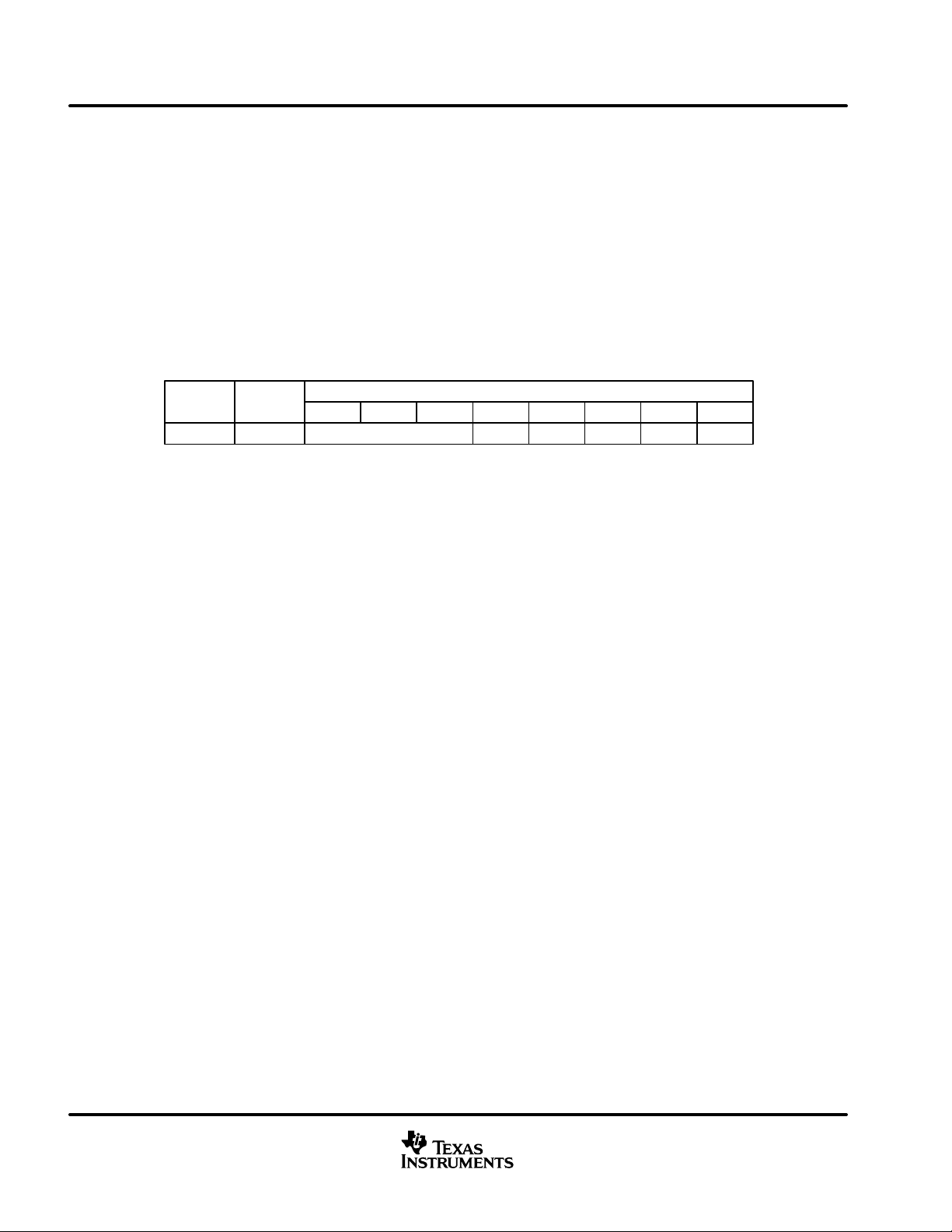
Table 7. Packet Configuration (24 bit)
ID (Bin) CMD (Bin)
DATA
MSB LSB
CCEN2 CCEN1 CCEN0RESERVEDxxxxxxxx 00100000
CONSTANT CURRENT OUTPUT
FOR COLOR TONE CORRECTION
TARGETEDTURN ON
COLOR TONE CORRECTION OFF
OUT1 (GOUT0) OUT0 (ROUT0)
OUT4 (GOUT1) OUT3 (ROUT1)
OUT7 (GOUT2) OUT6 (ROUT2)
OUT10 (GOUT3) OUT9 (ROUT3)
OUT2 (BOUT0) OUT0 (ROUT0)
OUT5 (BOUT1) OUT3 (ROUT1)
OUT8 (BOUT2) OUT6 (ROUT2)
OUT11 (BOUT3) OUT9 (ROUT3)
OUT0 (ROUT0)
OUT3 (ROUT1)
OUT6 (ROUT2)
OUT9 (ROUT3)
OUT2 (BOUT0)
OUT5 (BOUT1)
OUT8 (BOUT2)
OUT11 (BOUT3)
OUT0 (ROUT0)
OUT3 (ROUT1)
OUT6 (ROUT2)
OUT9 (ROUT3)
OUT1 (GOUT0)
OUT4 (GOUT1)
OUT7 (GOUT2)
OUT10 (GOUT3)
COLOR TONE CORRECTION OFF
OUT1 (GOUT0)
OUT4 (GOUT1)
OUT7 (GOUT2)
OUT10 (GOUT3)
OUT1 (GOUT0)
OUT4 (GOUT1)
OUT7 (GOUT2)
OUT10 (GOUT3)
OUT2 (BOUT0)
OUT5 (BOUT1)
OUT8 (BOUT2)
OUT11 (BOUT3)
OUT2 (BOUT0)
OUT5 (BOUT1)
OUT8 (BOUT2)
OUT11 (BOUT3)
0 0 0
0 0 1
0 1 0
0 1 1
1 0 0
1 0 1
1 1 0
1 1 1
UDG–02035
Only one combination is allowed to turn the color tone correction on or off in 1 HSYNC cycle. In other words,
when multiple combinations of correction is required, repeated color tone correction with required number of
gray scale display at one time is necessary. The following is example when all combinations for color tone
correction are needed. Since the current value of the constant-current output for basic display is determined
by the brightness adjustment data plus the dot correction data, the current value for color tone correction is
determined per pixel by the color tone correction data packet based on the current value excluding the dot
correction data after brightness adjustment, although it is different by the constant-current output depending
on dot correction data. Accordingly, the current value for color tone correction is shown as follows.
OUT0 (ROUT0) = OUT1 (GOUT0) = OUT2 (BOUT0), OUT3 (ROUT1) = OUT4 (GOUT1) = OUT5 (BOUT1)
OUT6 (ROUT2) = OUT7 (GOUT2) = OUT8 (BOUT2), OUT9 (ROUT3) = OUT10 (GOUT3) = OUT11 (BOUT3)
20
www.ti.com
Page 21

PRINCIPLES OF OPERATION
The following example shows all the combinations of color tone correction control with 8 gray scale.
SLLS528 – MARCH 2002
Figure 7. Color Tone Correction Control Combinations With 8–Bit Gray Scale
The timing of lighting-ON for the basic display to be turned on is delayed by t
The lighting-ON for color tone correction is turned on based on ON/OFF timing of output for color tone corrected.
www.ti.com
D(OUTn+1–OUTn)
until OUT1–OUT11.
21
Page 22

SLLS528 – MARCH 2002
PRINCIPLES OF OPERATION
operation mode setting
Using this packet, the same operation mode can be set to all the connected devices simultanoeously or different
operation modes can be set to each device.
Table 8. Packet Configuration (32-bit)
ID (Bin) CMD (Bin)
xxxxxxxx 01000000
MSB
RESERVED
DATA
LSB
F
R
D
L
S
G
S
L
D
K
C
D
E
E
N
N
E
B
S
C
E
E
R
N
V
E
D
F
O
O
R
R
C
C
E
E
O
O
F
N
F
OVM
DETECTION
VOLTAGE
SETTING
00 00
10 00
00 10
10 10
00 01
10 01
00 11
10 11
01 00
11 00
01 10
11 10
01 01
11 01
01 11
11 11
0.3 V
0.1 V
0.2 V
0.3 V
0.4 V
0.5 V
0.6 V
0.7 V
0.8 V
0.9 V
1.0 V
1.1 V
1.2 V
1/2 VCC
2/3 VCC
NO UPDATE
UDG–02037
22
00
NORMAL OPERATION
10
FORCE ALL OUTPUT ON
01
FORCE ALL OUTPUT OFF
11
INHIBIT
01SET BRIGHTNESS ADJUSTMENT TO 111111 (100%)
COMPLY WITH VALUE SET BY LATCH
01SET DOT CORRECTION TO 11111111 (100%)
COMPLY WITH VALUE SET BY LATCH
01LKD FUNCTION OFF
LKD FUNCTION ON
01USE INPUT CLOCK TO GCLK AS GRAY SCALE
USE INTERNAL CLOCK WITH INPUT CLOCK TO DTIN/STIN
www.ti.com
Page 23

Á
Á
Á
Á
Á
Á
SLLS528 – MARCH 2002
PRINCIPLES OF OPERATION
This packet allows DSG function, LKD function, dot correction function, brightness adjustment function, flag
setting for enable/disable to turn all the output on/off, and data setting for detection voltage set in the OVM
function.
DSG function (dual source gray scale clock)
The DSG function selects gray-scale clock from the input clock to GCLK terminal or internally-generated clock
using input to the DTIN/STIN terminals. By using the DSGSL flag in this packet, the signal used for the gray scale
clock is switched as below from next HSYNC packet. By using this function, the number of signal lines for gray
scale clock can be reduced, and display can be continued if DATA/STROBE lines are alive, even though the
gray scale clock has stopped due to any failures such as disconnection when using GCLK terminal.
The GEF/HEF function informs of any failures that may occur on the gray scale clock.
DSGSL=0: input clock to GCLK terminal (maximum operating frequency: 20 MHz)
DSGSL=1: internally generated clock using data input to DTIN/STIN terminals (maximum operating
frequency: 10 MHz)
LKD function
The LKD function supplies a constant-current of approximately 0.6 µA to the output terminal. When the power
supply voltage for the LED is 0 V (GND), writing a 1 to the LKDEN flag allows current flow through LED
subtracted leakage current of the device output transistor (below 0.1 µA) from 0.6 µA, and at this time the voltage
on output terminal decreases if the reverse leakage current occurs on LED. In this function, since maximum
applied voltage is 2.7 V, occurrence of reverse leakage current across LED can be found by reading the OVM
detection result through OVM information reading packet by setting the OVM detection voltage to 2/3 VCC. This
function should be used in combination with the FORCE OFF function to turn off all the constant-current outputs
off. The example for this function is shown in Table 9 below.
Table 9. LKD Function Sequence Example
1
Set LED power supply to 0 V (GND)
2
Set operation mode setting packet to force ON=0, force
Á
Á
ББББББББББББББ
OFF = 1 and LKDEN = 1
3
Wait at least 1 µs
4
Read OVM result through OVM information reading packet
5
Set operation mode setting paclet to force ON = 0, force
ББББББББББББББ
OFF = 0 and LKDEN = 0
Set OVM detection voltage and force all outputs OFF and
БББББББББББББ
LKD functions ON
Demand detection result
LKD function OFF and return to normal operation
БББББББББББББ
DCEN/BCEN
By writing 0 to the flag, the corresponding data (plane brightness data or dot correction data) is set to 100%
default value. By writing 1 to the flag, corresponding data is complied with the value set by data setting packet.
When both DCEN and BCEN are 0, the current value will be 100% of the value set by R
IREF
.
The function by flag setting becomes effective from next HSYNC packet after this packet, and in addition, when
both BCEN and DCEN flags are 1, the value set by respective data setting packets does not become effective
unless BCL and DCL flags in HSYNC packet are set to 1.
Setting bot h BCEN and DCEN flags to 0, doesn’t a f fect the latch flags in the HSYNC packet. This function writes
the default 1 to internal latch and the shift register is not updated. Therefore, unless the value for shift register
is updated in respective data setting packet, when plane brightness and dot correction functions are used next,
the previous status can be returned by latching the value of shift register into internal latch by setting BCL/DCL
flag in HSYNC packet after setting this packet.
www.ti.com
23
Page 24

SLLS528 – MARCH 2002
PRINCIPLES OF OPERATION
all output force off
By writing 0 to force-ON flag and 1 to force-OFF flag in this packet, all the outputs can be turned off
simultaneaously. Also, in this mode, by writing 0 to force-ON flag and 0 to force-OFF flag, it returns to the normal
operation.
all output force on
By writing 1 to force-ON flag and 0 to force-OFF flag in this packet, all the output are turned on independent
of the gray scale data from next HSYNC packet after this packet. At this time, the current value depends on the
plane brightness adjustment data and dot correction data. However, when both DCEN and BCEN are 0, it is
100% of the current value set by R
it returns to the normal operation after sending the HSYNC packet.
Table 10. All Outputs Forced ON Sequence Example
1
Plane brightness, dot corection data setting packet
2
Operation mode setting packet: force ON = 1 and force OFF = 0
3
HSYNC synchronization packet
4
Operation mode setting packet: force ON = 0 and force OFF = 0
5
HSYNC synchronization packet
. Also, in this mode, by writing 0 to force-ON flag and 0 to force-OFF flag,
IREF
Set desired value for output current.
Demand all output force ON.
Al outputs force ON.
Demand return to normal operation
Return to normal operation
Figure 8 shows the operation concept for this mode. All the constant-current outputs are turned on with the
current value set independent of the gray-scale data by HSYNC packet after writing 1 to force-ON flag and 0
to force-OFF flag in operation mode setting packet (these are not turned on if the dot correction value is 0). It
remains in that state independent of gray scale clock until all output force off mode in the packet is sent or
HSYNC packet is sent after writing 0 to force-ON flag and 0 to force-OFF flag in the packet.
24
www.ti.com
Page 25
PRINCIPLES OF OPERATION
ALL OUTPUT FORCE ON OPERATION
OPERATION
MODE SETTING
PACKET
FORCE ON = 1
FORCE OFF = 0
GRAY
SCALE
CLOCK
CONSTANT
CURRENT
OUTPUT
RELATION TO ALL OUTPUT FORCE OFF
NORMAL
LIGHT ON
OPERATION
MODE SETTING
PACKET
FORCE ON = 1
FORCE OFF = 0
HSYNC
PACKET
HSYNC
PACKET
OTHER
PACKET
OTHER
PACKET
FORCE ON
HSYNC
PACKET
DON’T CARE
OPERATION
MODE SETTING
PACKET
FORCE ON = 0
FORCE OFF = 1
OPERATION
OTHER
PACKET
IF DIFFERENT CURRENT VALUE IS SET
OTHER
PACKET
A
MODE SETTING
PACKET
FORCE ON = 0
FORCE OFF = 0
OPERATION
MODE SETTING
PACKET
FORCE ON = 0
FORCE OFF = 0
HSYNC
PACKET
OTHER
PACKET
A
SLLS528 – MARCH 2002
OTHER
PACKET
NORMAL
LIGHT ON
HSYNC
PACKET
GRAY
SCALE
CLOCK
CONSTANT
CURRENT
OUTPUT
NORMAL
LIGHT ON
LIGHT ON BY ALL
OUTPUT FORCE OFF
DON’T CARE
LIGHT OFF BY RELEASE OF ALL OUTPUT
FORCE ON (LATCHED BY HSYNC)
RE–LIGHT ON BY RELEASE OF
ALL OUTPUT FORCE OFF
FORCE ONFORCE ON
Figure 8. All Output Force ON Operation
Note that, in relation to all output force off shown in Figure 8, when the HSYNC packet is between the other
packet and operation mode setting packet with force-ON = 0 / force-OFF = 0, no re-light-ON happens by release
of all the output force-OFF.
OVM function
The OVM function is to compare the voltage across the constant-current output terminals (OUT0 to OUT11) with
the detection voltage set by this packet, and to output 0 as a comparison result if voltage across terminal is higher
than detection voltage and 1 if lower. The TLC5930 has one comparator per output as shown in Figure 9.
The comparison result input ORed with all the output appears in OVMFA of failure monitor information reading,
and result per output appears in OVM information reading data OVMF[0:1 1]. By using this function, where LED
disconnection (the voltage across output falls below 0.3 V) or LED short (the voltage across output goes
extremely high) has occurred can be detected. Also, the voltage across the constant-current output terminals
can be known when it is being turned on by changing the setting value of detection voltage, and heat-up from
the device can be minimized by controlling the voltage applied to the anode of the LED to minimize the voltage
across constant-current output (approximately 0.4 V at I
= 40 mA) based on the resulting voltage.
O
UDG–0203
www.ti.com
25
Page 26

Á
Á
Á
SLLS528 – MARCH 2002
PRINCIPLES OF OPERATION
OUT0
INTERNAL OUT0
LIGHT ON SIGNAL
INTERNAL OUT1
LIGHT ON SIGNAL
OUT1
.
.
.
OUT10
INTERNAL OUT10
LIGHT ON SIGNAL
+
OVMFA
+
.
.
.
.
.
.
.
.
.
+
OVMF[0]
OVMF[1]
.
.
.
OVMF[10]
INTERNAL OUT11
LIGHT ON SIGNAL
+
OVMF[11]
OUT11
+
COMPARISON
VOLTAGE
UDG–02039
Figure 9. OVM Function
The comparator works so that if a flag is set when read in its operation, voltage across the constant-current
output terminals is lower than the comparison voltage. However, the constant-current output is needed to be
turned on approximately 1 µs continuously until the comparator starts working. For this reason, the following
sequence is recommended to ensure the proper result.
Table 11. OVM Function Sequence Example
1
Gray-scale data, dot correction data setting packet
2
Operation mode setting packet: force ON = 1 and force
OFF = 0
3
HSYNC synchronization packet
4
Wait at least 1 µs
5
OVM information reading packet or failure monitor information
reading packet
6
Operation mode setting packet; force ON = 0 and force
Á
БББББББББББББ
OFF = 0
7
HSYNC synchronization packet
Set the desired value for output current.
Set OVM detection voltage and demand all output force ON.
Al outputs force ON.
Read OVM comparison result.
Demand return to normal operation.
ББББББББББББББ
Return to normal operation
26
www.ti.com
Page 27

SLLS528 – MARCH 2002
PRINCIPLES OF OPERATION
OVM information read
Using this packet, the comparison results between OVM detection voltage set by operation mode setting packet
and the each voltage across constant-current output terminal can be read by the individual constant-current
output terminals.
For individual IDs, each flag is information for each constant-current output for each specified device ID.
However for common ID devices, the ORed information for constant-current output terminals of devices is
connected in series. Data sent from the controller should be 0 as a dummy data except for ID and CMD. If the
flag is 1, it is passed through.
Table 12. Packet Configuration (32-bit)
ID (Bin) CMD (Bin)
xxxxxxxx 01010000 RESERVED
(xx500000h. PACKET SENT FROM CONTROLLER)
MSB
OVMF
[11]
OUT11 RESULT
OUT10 RESULT
OUT9 RESULT
OVMF
OVMF
[10]
[9]
OUT8 RESULT
OUT7 RESULT
DATA
OVMF
OVMF
[8]
[7]
OUT6 RESULT
OUT5 RESULT
OVMF
OVMF
[6]
[5]
OUT4 RESULT
OUT3 RESULT
OVMF
OVMF
[4]
[3]
OUT2 RESULT
OUT1 RESULT
OVMF
OVMF
[2]
[1]
OUT0 RESULT
LSB
OVMF
[0]
UDG–02040
www.ti.com
27
Page 28
SLLS528 – MARCH 2002
PRINCIPLES OF OPERATION
failure monitor information read
Using this packet, information is ORed when all outputs for OVM detection results, error flags for HEF, GEF,
TEF, and AWC flag can be read out. For individual IDs, each flag is information for each device, and for common
IDs, the information is ORed for devices connected in series. Although defective devices cannot be detected,
problems can be detected only by sending this packet periodically. Data other than AWC sent from controller
should be 0 as a dummy except ID and CMD. When the failure monitor information is 0, the input data (except
AWC) passes through. OVMFA and TEF are sent when this packet is sent. However , HEF and GEF are sent
when the HSYNC packet before this packet has been sent.
Table 13. Packet Configuration (24-bit)
ID (Bin) CMD (Bin)
xxxxxxxx 01100000 RESERVED OVMFA
(xx6000h.PACKET SENT FROM CONTROLLER)
DATA
LSBMSB
HEF GEF TEF AWC
UDG–02041
The default value for all the information is 1, so, note that 1 may be read out until normal lighting-ON starts after
the reset packet is sent.
OVMFA
The information ORed with detection results for all constant-current output in OVM function appears in this flag.
Although defective constant-current output cannot be identified by reading this flag, the OVM function detects
output errors.
HEF function (HSYNC Error Flag)
This function is to set 0 to HEF flag if the input number of gray-scale clock per 1 HSYNC cycle is more than 1024,
and 1 if less than 1025, at the time when the next HSYNC packet is sent. For example, when, despite the normal
gray-scale clock, the sending period of the HSYNC packet is shortened for any reason and the number of
gray-scale clock in 1 HSYNC cycle is less than 1025, that is, when the HSYNC packet is entered with the number
of gray-scale clock than 1025, HEF is set to 1. In other words, by using this function, one can know failure in
the HSYNC cycle. This function is assumed to use the TLC5930 for 1024 gray scale, and if use it less than 1025
such as 256 gray scale, this flag should be neglected even though it is always set to 1.
Regarding the number of the gray-scale clock needed for lighting-ON, a gray-scale clock total of 1025,
equivalent to 1024 plus 1, is needed to complete lighting on with 1024 gray-scale clock, since lighting on starts
with second rising edge of gray-scale clock after LSB input of the HSYNC packet.
GEF function (GCLK Error Flag)
This function is to set 0 to GEF flag if the number of gray-scale clock meet the requied number of gray-scale
per 1 HSYNC cycle, and 1 if not, at the time when the next HSYNC packet is sent. For example, when the
gray-scale data f o r g i ven constant-current output is 100, and the gray-scale clock is entered between 2 and 100
for each HSYNC cycle, the correcponding constant-current output remains in an on–state until the next HSYNC
packet is sent. When the clock is less than 2, the output is not turned on. In this case, if lighting-ON for the number
of gray-scale clock is not done, GEF is set to 1 assumed as failure. In other words, by using this function, one
can know whether the gray scale clock is normally sent or 1 HSYNC cycle meet the lighting-ON time desired.
Notes that this flag is set to 1 independent of the status of the gray-scale clock during one HSYNC cycle after
all outputs are forced on.
28
www.ti.com
Page 29

SLLS528 – MARCH 2002
PRINCIPLES OF OPERATION
failure monitor information read (continued)
TEF function (thermal error flag)
This function, is used to determine when the junction temperature of the device exceeds its limit. This function
sets 0 to the TEF flag if the junction temperature is less than 160_C, and set it to 1 if the temperature is greater
than 160_C.
AWC function (active wire check)
This function is used to check that the communication between controller and driver is performing normally. The
TLC5930 clocks out the inverted data from written data into bits when this packet is entered. For individual IDs,
the inverted data from the controller output returns to the controller. For common IDs, the same data as the
controller output returns to the controller if the number of devices connected in series is even, but returns to the
inverted data if it is odd.
read information output
For failure monitor information reading (including OVM information reading, failure monitor information flags in
the HSYNC packet), for individual IDs or common IDs, it is set to 1 if an error is indicated. Input data is passed
through if there is no error detected. For A WC, for both individual and common IDs, the inverted data from input
data is clocked out. When the ID is neither common nor matched, the data including AWC is passed through.
Table 16 shows four connected device. Bold bits indicates the reading information output from the device.
Table 14. Read Information Output
DEVICE NUMBER
IC1 INPUT (CONTROLLER OUTPUT)
IC1 OUTPUT (IC2 INPUT)
IC2OUTPUT (IC3 INPUT)
IC3 OUTPUT (IC4 INPUT)
IC4 OUTPUT (CONTROLLER INPUT)
DEVICE
NUMBER
IC1 INPUT
IC1 OUTPUT
IC2 OUTPUT
IC3 OUTPUT
IC4 OUTPUT
DEVICE
NUMBER
IC1 INPUT
IC1 OUTPUT
IC2 OUTPUT
IC3 OUTPUT
IC4 OUTPUT
ID
NO.
1
ID
NO.
3
DATA BIT 111111111122222222223333
.123456789012345678901234567890123
x000000010110000000000000xxxxxxxxx
xxx000000010110000000010001xxxxxxx
xxxxx000000010110000000010001xxxxx
xxxxxxx000000010110000000010001xxx
xxxxxxxxx000000010110000000010001x
DATA BIT 111111111122222222223333
.123456789012345678901234567890123
x000000110110000000000000xxxxxxxxx
xxx000000110110000000000000xxxxxxx
xxxxx000000110110000000000000xxxxx
xxxxxxx000000110110000000001101xxx
xxxxxxxxx000000110110000000001101x
CONDITION
IC1: OVM fail
IC2: ALL PASS
IC3: HEF, GEF fail
IC4: ALL PASS
ID
NO.
COMM
ON
ID
NO.
2
ID
NO.
4
DATA BIT 111111111122222222223333
.123456789012345678901234567890123
x000000000110000000000000xxxxxxxxx
xxx000000000110000000010001xxxxxxx
xxxxx000000000110000000010000xxxxx
xxxxxxx000000000110000000011101xxx
xxxxxxxxx000000000110000000011100x
DATA BIT 111111111122222222223333
.123456789012345678901234567890123
x000000100110000000000000xxxxxxxxx
xxx000000100110000000000000xxxxxxx
xxxxx000000100110000000000001xxxxx
xxxxxxx000000100110000000000001xxx
xxxxxxxxx000000100110000000000001x
DATA BIT 111111111122222222223333
.123456789012345678901234567890123
x000001000110000000000000xxxxxxxxx
xxx000001000110000000000000xxxxxxx
xxxxx000001000110000000000000xxxxx
xxxxxxx000001000110000000000000xxx
xxxxxxxxx000001000110000000000001x
www.ti.com
29
Page 30

SLLS528 – MARCH 2002
PRINCIPLES OF OPERATION
automatic ID setting
The device that receives this packet stops DTOUT and STOUT for 8 bits (ID portion in below packet
configuration) after CMD, and recognizes the 8 bits as its own ID. Next, 8 bits data with recognized ID plus 1
bit is clocked out, and dummy data sent is passed through until 03h data is entered. When the device receives
03h data, it recognizes the ID setting completion and is ready to receive the next command. During reception
of the next 8 bits each device receives, DATA/STROBE output is inhibited, so the controller must send dummy
data (0) with bit counts of at least minimum device number times 8 bit after ID/CMD/DATA(ID) until this packet
operation is completed including DTOUT/STOUT output.
Table 15. Packet Configuration (32-bit + 8-bit (IC–1))
ID (Bin) CMD (Bin)
00000000 01110000 xxxxxxxx
(0070xxh + 00h × IC NUMBER + 03h)
ID DUMMY END
DATA (BIN)
00000000 × IC NUMBER
00000011
UDG–02043
The following is a sequence example for automatic ID setting (in the case of one device and four devices). In
this example, IC1 input indicates output from the controller, while the last device output indicates the input for
the controller. Since the blank portion in the example does not recognize the input in DS-LINK, input to controller
is continuous ID/CMD/DATA(DATA=number of devices + 1). There are two different methods to send
DATA(END) 03h;
D Calculate and send the number of dummy data as the number of devices times 8 bits.
D Stop the dummy data output synchronizing with receiving the ID/CMD/DATA(DATA=number of devices +
1) at the controller input and send DATA 03h.
The latter case is useful when the number of connected devices is unknown (for automatic recognition). The
number of devices connected that can be known from that DATA(ID) received by the controller shows the
number of devices plus 1. In any case, dummy data should be an 8-bit base.
Table 16. One IC (No Dummy Data)
IC NUMBER DATA BIT
IC1 INPUT
IC1 OUTPUT
..............1111111111222222222233333333334444
.....1234567890123456789012345678901234567890123.....
xxxxx0000000001110000000000010000001100000011xxxxx
xxxxxxx0000000001110000........0000001000000011xxx
30
IC NUMBER DATA BIT
IC1 INPUT
IC1 OUTPUT (IC2 INPUT)
IC2 OUTPUT (IC3 INPUT)
IC3 OUTPUT (IC4 INPUT)
IC4 OUTPUT
Table 17. Four ICs (24-bit Dummy Data)
..............11111111112222222222333333333344444444445555555555666666666677
.....12345678901234567890123456789012345678901234567890123456789012345678901..
xxxxx0000000001110000000000010000000000000000000000000000000000000011xxxxxxxxx
xxxxxxx0000000001110000........0000001000000000000000000000000000000011xxxxxxx
xxxxxxxxx00000000011100........00........00000011000000000000000000000011xxxxx
xxxxxxxxxxx000000000111........00........00........000001000000000000000011xxx
xxxxxxxxxxxxx0000000001........11........00........00........0000010100000011x
www.ti.com
Page 31

ÁÁÁ
ÁÁÁ
ÁÁÁ
ÁÁÁ
SLLS528 – MARCH 2002
PRINCIPLES OF OPERATION
HSYNC synchronization
The constant-current output is turned on, synchronizing with this packet. In addition, for common IDs, the failure
monitor information flag is read out through the 5 LSB of DA TA within the packet (see failure monitor information
read section), and data written in the internal register within gray scale data setting packet, plane brightness
adjustment data setting packet, dot correction data setting packet, color tone correction setting packet, and color
tone correction control setting packet are latched, depending on the status of the register latch flag of 5 MSB
of DATA. Since each flag in the register latch flag is independent, writing a 1 allows the respective packet data
to be latched. Writing a 0 to the flag allows no latch. By using this function, gray scale data, plane brightness
adjustemnt data , dot correction data, color–tone correction, and correction control setting packets can be sent
asynchronously with the HSYNC cycle.
Note that no lighting-ON occurs when the gray-scale clock is entered before this HSYNC packet of normal
lighting-ON operation (including use of internally generated clock) during the first normal lighting-ON operation
(PWM operation) after power up. Normal operation occurs after the second operation.
Table 18. Packet Configuration (32-bit)
ID (Bin) CMD (Bin)
00000000 10000000
(0080xxh.PACKET SENT FORM CONTROLLER)
REGISTER LATCH FLAG DATA FAILURE MONITOR FLAG
MSB LSB
OVMFA
REFER FAILURE MONITOR READ
1
1
1
LATCH COLOR TONE CORRECTION DATA
LATCH PLANE BRIGHTNESS ADJUSTMENT DATA1
CORRECTION CONTROL DATA
LATCH DOT CORRECTION DATA
LATCH COLOR TONE
LATCH GRAY SCALE DATA1
NO LATCH0 0 0 0 0
HEF GEF TEF AWCRESERVEDGSL BCL DCL CCL CSL
Table 21 shows the relationship between failure monitor information reading packet, HSYNC packet, and other
various error flags.
Table 19. Error Flag Relationships
TIME
HSYNC
PACKET
1
1
1
1
FAIL
RELEASE
FAILURE
PACKET
0
1
1
0
HSYNC
PACKET
0
0
0
0
FAIL
OCCUR
HSYNC
PACKET
1
1
1
1
FAILURE
PACKET
1
1
1
1
FAIL
RELEASE
HSYNC
PACKET
0
0
0
0
OVMFA
HEF
GEF
TEF
FAIL
OCCUR
FAILURE
PACKET
1
0
0
1
UDG–02044
FAILURE
PACKET
0
0
0
0
www.ti.com
31
Page 32

Á
Á
S
{
Á
SLLS528 – MARCH 2002
PRINCIPLES OF OPERATION
calculating constant-current output
The current value of constant-current output can be calculated using the following expression.
I
OLC (n)
Where IDC is main current (except color tone correction), ICC is color tone correction current. Both currents are
referenced with reference current, I
I
from color tone correction data and color tone correction control data. n is output terminal number, 0 to 11.
CC
reference current
The reference current I
brightness data, r
I
IREF
VȀ
IREF
+ 42ǒI
+ 4
+
) I
DC (n)
can be calculated with external resistor, R
IREF
, using the following expression.
BC
VȀ
IREF
ǒ
ȱ
0.4 )
ȧ
R
Ǔ
IREF
0.6ǒrBC) 1
ǒ
Ȳ
main current
The main current, I
scale data, and reference current, I
+
I
DC (n)
, can be calculated with dot correction data, rDC, logic signal, S
DC
ǒ
r
DC (n)
256
Ǔ
S
MAIN (n)
CC (n)
64
Ǔ
(IREF)
Ǔ
Ǔ
, and I
ȳ
V
ȧ
is established by dot correction data and gray scale data.
(DC)
IREF
ȴ
, using the following expression.
IREF
I
IREF
, voltage reference, V
IREF
IREF
, established by gray
MAIN
(2)
, and plane
(3)
(4)
(5)
Where S
ÁÁÁÁÁБББББ
MAIN (n) =
ÁÁÁÁ
, is set to following value depending on gray scale data, rGC.
MAIN
1: r
0: r
БББББ
GC (n)
GC (n)
> 0
= 0
32
www.ti.com
Page 33

Á
S
{
Á
S
{
Á
S
{
Á
Á
S
{
Á
Á
S
{
Á
Á
S
{
Á
PRINCIPLES OF OPERATION
color tone correction current
SLLS528 – MARCH 2002
The color tone correction current, I
logic signal, S
, for color tone correction current switch established by the combination of color tone correction
CC
, can be calculated with I′CC established by color tone correction data, and
CC
control data with logic signal for main current switch, using the following expression.
is expressed depending on color tone correction data r
I′
CC
r
IȀ
IȀ
IȀ
IȀ
CC(9)
CC(0)
CC(3)
CC(6)
+ IȀ
+ IȀ
+ IȀ
+ IȀ
CC(1)
CC(4)
CC(7)
CC(10)
+ IȀ
+ IȀ
+ IȀ
+ IȀ
CC(2)
CC(5)
CC(8)
CC(11)
+
2
+
2
+
2
+
ǒ
4 * r
ǒ
4 * r
ǒ
4 * r
ǒ
2
1
1
1
4 * r
CC1[7:6]
CC2[7:6]
CC3[7:6]
1
CC4[7:6]
SCC is set up by color tone correction control switch, S
r
and S
CCEN
БББББÁББББББББББББ
CCEN1 =
MAIN
. S
is expressed as follows:
CCEN
1: r
CCEN
=0 0 1 (bin)
Ǔ
Ǔ
Ǔ
Ǔ
CCEN
CC1[5:0]
r
CC2[5:0]
r
CC3[5:0]
r
CC1
64
64
64
CC4[5:0]
64
through r
I
IREF
I
IREF
I
IREF
I
IREF
as follows.
CC4
, established by color tone correction control data
0: except the above
(6)
(7)
(8)
(9)
БББББÁББББББББББББ
CCEN2 =
1: r
CCEN
=0 1 0 (bin)
0: except the above
БББББÁББББББББББББ
CCEN3 =
1: r
CCEN
=0 1 1 (bin)
0: except the above
БББББÁББББББББББББ
CCEN4 =
1: r
CCEN
=1 0 0 (bin)
0: except the above
БББББ
CCEN5 =
БББББ
CCEN6 =
БББББ
ББББББББББББ
1: r
0: except the above
ББББББББББББ
1: r
0: except the above
ББББББББББББ
CCEN
CCEN
=1 0 1 (bin)
=1 1 0 (bin)
www.ti.com
33
Page 34

Á
S
{
Á
Á
S
{
Á
Á
S
{
Á
Á
S
{
Á
S
{
Á
S
{
Á
Á
S
{
Á
Á
S
{
Á
Á
S
{
Á
Á
S
{
Á
Á
S
{
Á
Á
S
{
SLLS528 – MARCH 2002
PRINCIPLES OF OPERATION
1: (S
CC[0] =
ÁÁÁÁ
CC[1] =
ÁÁÁÁ
CC[2] =
ÁÁÁÁ
ÁÁÁÁÁББББББББББББББББББББ
CC[3] =
CCEN3
0: except the above
ББББББББББББББББББББ
1: (S
CCEN1
0: except the above
ББББББББББББББББББББ
1: (S
CCEN2
0: except the above
ББББББББББББББББББББ
1: (S
CCEN3
and S
and S
and S
and S
MAIN[1]
MAIN[0]
MAIN[0]
MAIN[4]
) or (S
) or (S
) or (S
) or (S
CCEN5
CCEN6
CCEN4
CCEN5
and S
and S
and S
and S
MAIN[2]
MAIN[2]
MAIN[1]
MAIN[5]
) = TRUE
) = TRUE
) = TRUE
) = TRUE
0: except the above
ÁÁÁÁÁББББББББББББББББББББ
CC[4] =
1: (S
CCEN1
and S
MAIN[3]
) or (S
CCEN6
and S
MAIN[5]
) = TRUE
0: except the above
ÁÁÁÁÁББББББББББББББББББББ
CC[5] =
1: (S
CCEN2
and S
MAIN[3]
) or (S
CCEN4
and S
MAIN[4]
) = TRUE
0: except the above
ÁÁÁÁÁББББББББББББББББББББ
CC[6] =
1: (S
CCEN3
and S
MAIN[7]
) or (S
CCEN5
and S
MAIN[8]
) = TRUE
0: except the above
ÁÁÁÁ
ББББББББББББББББББББ
1: (S
CC[7] =
ÁÁÁÁ
CC[8] =
ÁÁÁÁ
CC[9] =
ÁÁÁÁ
CC[10] =
ÁÁÁÁ
ÁÁÁÁÁББББББББББББББББББББ
CC[11] =
CCEN1
0: except the above
ББББББББББББББББББББ
1: (S
CCEN2
0: except the above
ББББББББББББББББББББ
1: (S
CCEN3
0: except the above
ББББББББББББББББББББ
1: (S
CCEN1
0: except the above
ББББББББББББББББББББ
1: (S
CCEN2
and S
and S
and S
and S
and S
MAIN[6]
MAIN[6]
MAIN[10]
MAIN[9]
MAIN[9]
) or (S
) or (S
) or (S
) or (S
) or (S
CCEN6
CCEN4
CCEN5
CCEN6
CCEN4
and S
and S
and S
and S
and S
MAIN[8]
MAIN[7]
MAIN[11]
MAIN[10]
MAIN[11]
) = TRUE
) = TRUE
) = TRUE
) = TRUE
) = TRUE
0: except the above
34
www.ti.com
Page 35

PRINCIPLES OF OPERATION
SLLS528 – MARCH 2002
Table 20. Register Term Summary
DATA
r
BC
r
DC
r
GC
r
CC1
r
CC2
r
CC3
r
CC4
r
CCEN
FUNCTION
Plane brightness adjustment data set by plane brightness adjustment data setting packet
Dot correction data set by dot correction data setting packet
Gray scale data set by gray scale data setting packet
Color tone correction data for pixel 1 set by color tone correction data setting packet
Color tone correction data for pixel 2 set by color tone correction data setting packet
Color tone correction data for pixel 3 set by color tone correction data setting packet
Color tone correction data for pixel 4 set by color tone correction data setting packet
Color tone correction control flag set by color tone correction control setting packet
www.ti.com
35
Page 36

36
ÖÖ
ÖÖ
ÖÖ
ÖÖ
ÖÖ
ÖÖ
ÖÖ
ÖÖ
ÖÖ
ÖÖ
ÖÖ
ÖÖ
ÖÖ
ÖÖ
Ö
Ö
Ö
Ö
Ö
Ö
Ö
Ö
Ö
Ö
Ö
Ö
Ö
Ö
Ö
Ö
SLLS528 – MARCH 2002
www.ti.com
Timing chart 1
Input data
(when external gray scale clock is used)
GSL BCL DCL CCL CSL HEF GEF TEF AWC
HSYNC PACKET
OVMFA
Figure 10. Timing Diagrams (External Gray-Scale CLock)
DTIN
1/tDATA tEDGE
STIN
Output data
GSL BCL DCL CCL CSL
1
1 1 1 1 0 0 0 0 0 0 0 0 000 0
DTOUT
tD(D/SIN–D/SOUT)
STOUT
GCLK
tD(D/SIN–OUT0)
OUT0 Driver ON
tD(OUTn+1–OUTn) tD(OUTn+1–OUTn)
Hsync packet
Driver OFF
HEF GEF TEF AWC
OVMFA
2nd rising edge
tSU(HSYNC–GCLK)
tD(GCLK–OUT0)
Next packet
0
0 0 0 1 0 0 0 11 1 1 1 1 0 0 0 0 0 0 0 0 0 0 00
Next packet
0 0 0 1 0 00 1
0
By AWC function, inverted data from
1/fGCLK
tWH(GCLK)
input is clocked out
tWL(GCLK)
tD(GCLK–OUT0)
Driver OFF(OUT0:G/S data9)
OUT1 Driver ON
OUT11 Driver ON
When in all output force on or number of gray scale clock is less than data count
Driver OFF
Driver OFF
Page 37

ÖÖ
ÖÖ
ÖÖ
ÖÖ
ÖÖ
ÖÖ
ÖÖ
ÖÖ
ÖÖ
ÖÖ
ÖÖ
ÖÖ
ÖÖ
ÖÖ
ÖÖ
ÖÖ
ÖÖ
ÖÖ
ÖÖ
ÖÖ
ÖÖ
ÖÖ
ÖÖ
ÖÖ
ÖÖ
ÖÖ
ÖÖ
ÖÖ
ÖÖ
ÖÖ
ÖÖ
T iming chart 2 (when internal gray scale clock is used)
www.ti.com
Input data
GSL BCL DCL CCL CSL HEF GEF TEF AWC
Figure 11. Timing Diagrams (Internal Gray-Scale Clock)
HSYNC packet
OVMFA
Next packet
0
0 0 0 1 0 0 0 11 1 1 1 1 0 0 0 0 0 0 0 0 0 0 10 0 0 0 0
DTIN
1/tDATA
STIN
Output data
GSL BCL DCL CCL CSL HEF GEF TEF AWC
1
1 1 1 1 0 0 0 0 0 0 0 0 000 0
HSYNC packet
OVMFA
Next packet
DTOUT
tD(D/SIN–D/SOUT)
By AWC function, inverted data from input is clocked out
STOUT
4th edge from edge of D/SIN HSYNC packet LSB
tD(D/SIN–OUT0)
OUT0 Driver ON
Driver OFF
tD(OUTn+1–OUTn) tD(OUTn+1–OUTn)
0
tEDGE
0 0 0 1 0 00 0
tD(D/SIN–OUT0)
0 1 00
tD(D/SIN–OUT0)
Driver OFF(OUT0:G/S data3)
37
OUT1 Driver ON
OUT11 Driver ON
When in all output force on or number of gray-scale closk is less than data count
Driver OFF
Driver OFF
SLLS528 – MARCH 2002
Page 38

MHTS001D – JANUARY 1995 – REVISED MAY 1999
PWP (R-PDSO-G**) PowerPAD PLASTIC SMALL-OUTLINE
20 PINS SHOWN
0,65
20
1
1,20 MAX
0,30
0,19
11
4,50
4,30
10
A
0,15
0,05
PINS **
DIM
M
0,10
6,60
6,20
Seating Plane
0,10
1614
Thermal Pad
(See Note D)
20
0,15 NOM
0°–ā8°
Gage Plane
0,25
0,75
0,50
2824
A MAX
A MIN
NOTES: A. All linear dimensions are in millimeters.
B. This drawing is subject to change without notice.
C. Body dimensions do not include mold flash or protrusions.
D. The package thermal performance may be enhanced by bonding the thermal pad to an external thermal plane.
This pad is electrically and thermally connected to the backside of the die and possibly selected leads.
E. Falls within JEDEC MO-153
PowerPAD is a trademark of Texas Instruments Incorporated.
5,10
4,90
5,10
4,90
6,60
6,40
7,90
7,70
9,80
9,60
4073225/F 10/98
38
www.ti.com
Page 39

PACKAGE OPTION ADDENDUM
www.ti.com
18-Jul-2006
PACKAGING INFORMATION
Orderable Device Status
(1)
Package
Type
Package
Drawing
Pins Package
Qty
Eco Plan
TLC5930PWP ACTIVE HTSSOP PWP 24 60 Green (RoHS &
no Sb/Br)
TLC5930PWPG4 ACTIVE HTSSOP PWP 24 60 Green (RoHS &
no Sb/Br)
TLC5930PWPR ACTIVE HTSSOP PWP 24 2000 Green (RoHS &
no Sb/Br)
TLC5930PWPRG4 ACTIVE HTSSOP PWP 24 2000 Green (RoHS &
no Sb/Br)
(1)
The marketing status values are defined as follows:
ACTIVE: Product device recommended for new designs.
LIFEBUY: TI has announced that the device will be discontinued, and a lifetime-buy period is in effect.
NRND: Not recommended for new designs. Device is in production to support existing customers, but TI does not recommend using this part in
a new design.
PREVIEW: Device has been announced but is not in production. Samples may or may not be available.
OBSOLETE: TI has discontinued the production of the device.
(2)
Eco Plan - The planned eco-friendly classification: Pb-Free (RoHS), Pb-Free (RoHS Exempt), or Green (RoHS & no Sb/Br) - please check
http://www.ti.com/productcontent for the latest availability information and additional product content details.
TBD: The Pb-Free/Green conversion plan has not been defined.
Pb-Free (RoHS): TI's terms "Lead-Free" or "Pb-Free" mean semiconductor products that are compatible with the current RoHS requirements
for all 6 substances, including the requirement that lead not exceed 0.1% by weight in homogeneous materials. Where designed to be soldered
at high temperatures, TI Pb-Free products are suitable for use in specified lead-free processes.
Pb-Free (RoHS Exempt): This component has a RoHS exemption for either 1) lead-based flip-chip solder bumps used between the die and
package, or 2) lead-based die adhesive used between the die and leadframe. The component is otherwise considered Pb-Free (RoHS
compatible) as defined above.
Green (RoHS & no Sb/Br): TI defines "Green" to mean Pb-Free (RoHS compatible), and free of Bromine (Br) and Antimony (Sb) based flame
retardants (Br or Sb do not exceed 0.1% by weight in homogeneous material)
(2)
Lead/Ball Finish MSL Peak Temp
CU NIPDAU Level-2-260C-1 YEAR
CU NIPDAU Level-2-260C-1 YEAR
CU NIPDAU Level-2-260C-1 YEAR
CU NIPDAU Level-2-260C-1 YEAR
(3)
(3)
MSL, Peak Temp. -- The Moisture Sensitivity Level rating according to the JEDEC industry standard classifications, and peak solder
temperature.
Important Information and Disclaimer:The information provided on this page represents TI's knowledge and belief as of the date that it is
provided. TI bases its knowledge and belief on information provided by third parties, and makes no representation or warranty as to the
accuracy of such information. Efforts are underway to better integrate information from third parties. TI has taken and continues to take
reasonable steps to provide representative and accurate information but may not have conducted destructive testing or chemical analysis on
incoming materials and chemicals. TI and TI suppliers consider certain information to be proprietary, and thus CAS numbers and other limited
information may not be available for release.
In no event shall TI's liability arising out of such information exceed the total purchase price of the TI part(s) at issue in this document sold by TI
to Customer on an annual basis.
Addendum-Page 1
Page 40

IMPORTANT NOTICE
Texas Instruments Incorporated and its subsidiaries (TI) reserve the right to make corrections, modifications,
enhancements, improvements, and other changes to its products and services at any time and to discontinue
any product or service without notice. Customers should obtain the latest relevant information before placing
orders and should verify that such information is current and complete. All products are sold subject to TI’s terms
and conditions of sale supplied at the time of order acknowledgment.
TI warrants performance of its hardware products to the specifications applicable at the time of sale in
accordance with TI’s standard warranty. Testing and other quality control techniques are used to the extent TI
deems necessary to support this warranty . Except where mandated by government requirements, testing of all
parameters of each product is not necessarily performed.
TI assumes no liability for applications assistance or customer product design. Customers are responsible for
their products and applications using TI components. To minimize the risks associated with customer products
and applications, customers should provide adequate design and operating safeguards.
TI does not warrant or represent that any license, either express or implied, is granted under any TI patent right,
copyright, mask work right, or other TI intellectual property right relating to any combination, machine, or process
in which TI products or services are used. Information published by TI regarding third-party products or services
does not constitute a license from TI to use such products or services or a warranty or endorsement thereof.
Use of such information may require a license from a third party under the patents or other intellectual property
of the third party, or a license from TI under the patents or other intellectual property of TI.
Reproduction of information in TI data books or data sheets is permissible only if reproduction is without
alteration and is accompanied by all associated warranties, conditions, limitations, and notices. Reproduction
of this information with alteration is an unfair and deceptive business practice. TI is not responsible or liable for
such altered documentation.
Resale of TI products or services with statements different from or beyond the parameters stated by TI for that
product or service voids all express and any implied warranties for the associated TI product or service and
is an unfair and deceptive business practice. TI is not responsible or liable for any such statements.
Following are URLs where you can obtain information on other Texas Instruments products and application
solutions:
Products Applications
Amplifiers amplifier.ti.com Audio www.ti.com/audio
Data Converters dataconverter.ti.com Automotive www.ti.com/automotive
DSP dsp.ti.com Broadband www.ti.com/broadband
Interface interface.ti.com Digital Control www.ti.com/digitalcontrol
Logic logic.ti.com Military www.ti.com/military
Power Mgmt power.ti.com Optical Networking www.ti.com/opticalnetwork
Microcontrollers microcontroller.ti.com Security www.ti.com/security
Low Power Wireless www.ti.com/lpw Telephony www.ti.com/telephony
Video & Imaging www.ti.com/video
Wireless www.ti.com/wireless
Mailing Address: Texas Instruments
Post Office Box 655303 Dallas, Texas 75265
Copyright 2006, Texas Instruments Incorporated
 Loading...