

TLC5921
LED DRIVER
SLLS390 – SEPTEMBER 1999
1
POST OFFICE BOX 655303 • DALLAS, TEXAS 75265
D
Drive Capability and Output Counts
– 80 mA (Current Sink) x 16 Bits
D
Constant Current Output Range
– 1 to 80 mA (C urrent Value Setting for All
Output Terminals Using External Resistor)
D
Constant Current Accuracy
– ±1% (Typ)
– ±4% (Max) (Maximum Error Between
Bits, All Bits On)
D
Voltage Applied to Constant Current Output
Terminal
– Minimum 0.6 V (Output Current 40 mA)
– Minimum 1 V (Output Current 80 mA)
D
Data Input
– Clock Synchronized 1 Bit Serial Input
D
Data Output
– Clock Synchronized 1 bit Serial Output
(With Timing Selection)
D
Input/Output Signal Level . . . CMOS Level
D
Power Supply V oltage . . . 4.5 V to 5.5V
D
Maximum Output Voltage . . . 17 V (Max)
D
Data Transfer Rate . . . 20 MHz (Max)
D
Operating Free-Air Temperature Range
–20°C to 85°C
D
Available in 32 Pin HTSSOP DAP Package
(PD=3.9 W,
T
A
= 25°C)
D
LOD Function . . . LED Open Detection
(Error Signal Output at LED Disconnection)
D
TSD Function . . . Thermal Shutdown (Turn
Output Off When Junction Temperature
Exceeds Limit)
description
The TLC5921 is a current-sink constant current driver incorporating shift register and data latch. The current
value at constant current output can be set by one external register. The device also incorporates thermal
shutdown (TSD) circuitry which turns constant current output off when the junction temperature exceeds the
limit, and LED open detection (LOD) circuitry to report the LED was disconnected.
Copyright 1999, Texas Instruments Incorporated
PRODUCTION DATA information is current as of publication date.
Products conform to specifications per the terms of Texas Instruments
standard warranty. Production processing does not necessarily include
testing of all parameters.
Please be aware that an important notice concerning availability, standard warranty, and use in critical applications of
Texas Instruments semiconductor products and disclaimers thereto appears at the end of this data sheet.
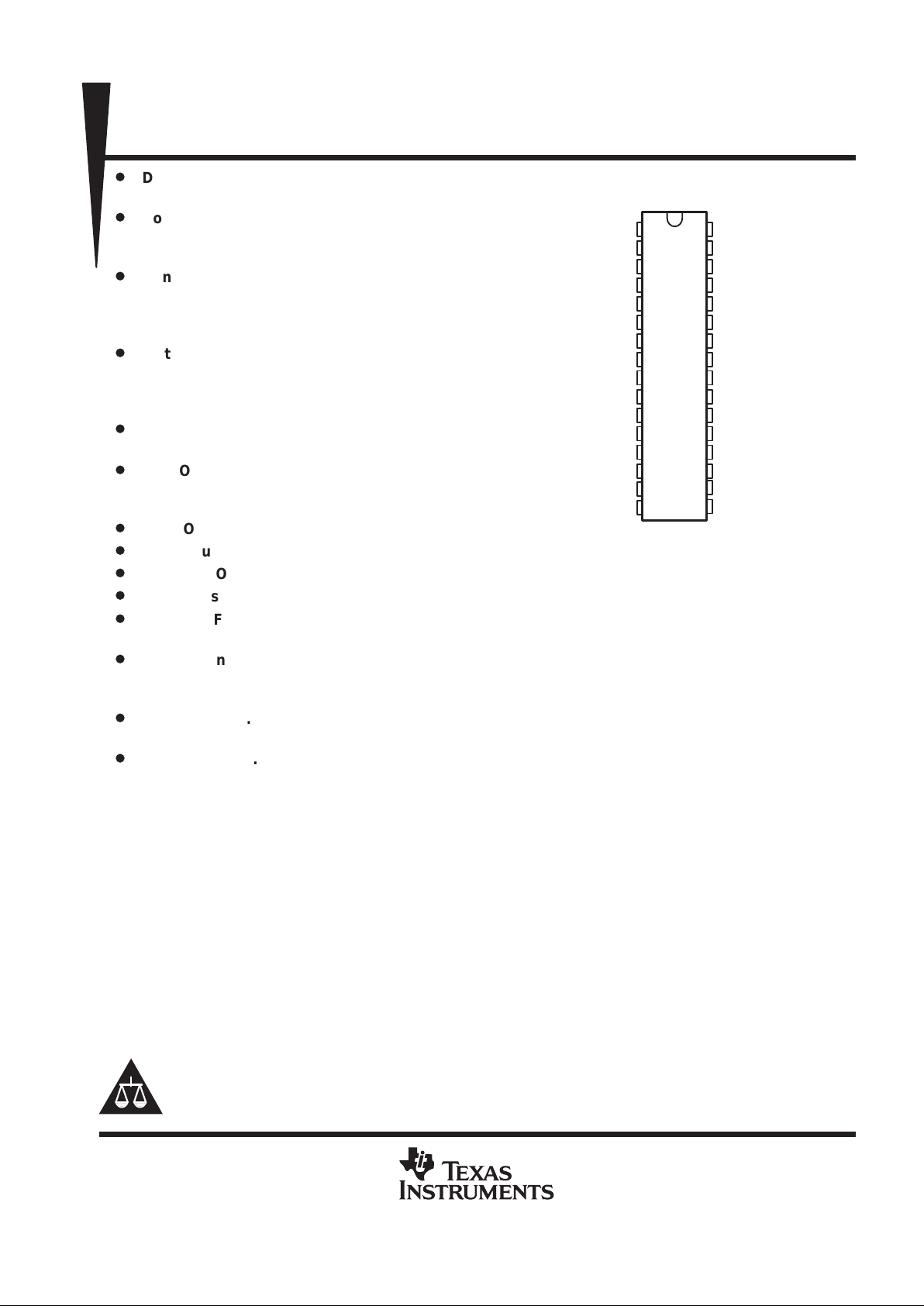
1
2
3
4
5
6
7
8
9
10
11
12
13
14
15
16
32
31
30
29
28
27
26
25
24
23
22
21
20
19
18
17
GND
BLANK
XLAT
SCLK
SIN
PGND
OUT0
OUT1
PGND
OUT2
OUT3
OUT4
OUT5
PGND
OUT6
OUT7
VCC
IREF
SOMODE
XDOWN
SOUT
PGND
OUT15
OUT14
PGND
OUT13
OUT12
OUT11
OUT10
PGND
OUT9
OUT8
(TOP VIEW)
DAP PACKAGE
TLC5921
LED DRIVER
SLLS390 – SEPTEMBER 1999
2
POST OFFICE BOX 655303 • DALLAS, TEXAS 75265
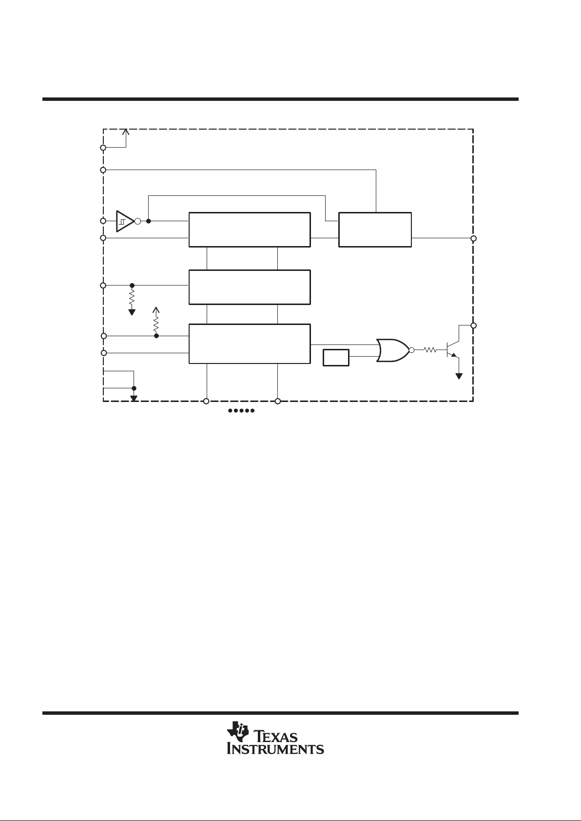
functional block diagram
Timing Selector
16 bits
Data Latch
XLAT
SOUT
OUT0 OUT15
SOMODE
SCLK
SIN
16 bits
Shift Register
16 bits Constant Current Driver
and
LED Disconnection detection
BLANK
IREF
TSD
XDOWN
VCC
GND
PGND
100 kΩ
100 kΩ
TLC5921
LED DRIVER
SLLS390 – SEPTEMBER 1999
3
POST OFFICE BOX 655303 • DALLAS, TEXAS 75265
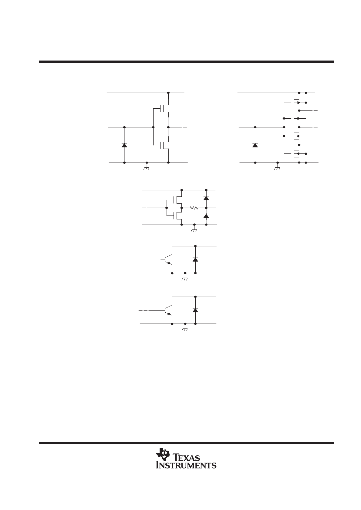
equivalent input and output schematic diagrams
VCC
Input (except SCLK)
INPUT
GND
SOUT
VCC
OUTPUT
GND
XDOWN
GND
XDOWN
OUTn
GND
OUTn
VCC
INPUT
GND
Input (SCLK)
TLC5921
LED DRIVER
SLLS390 – SEPTEMBER 1999
4
POST OFFICE BOX 655303 • DALLAS, TEXAS 75265
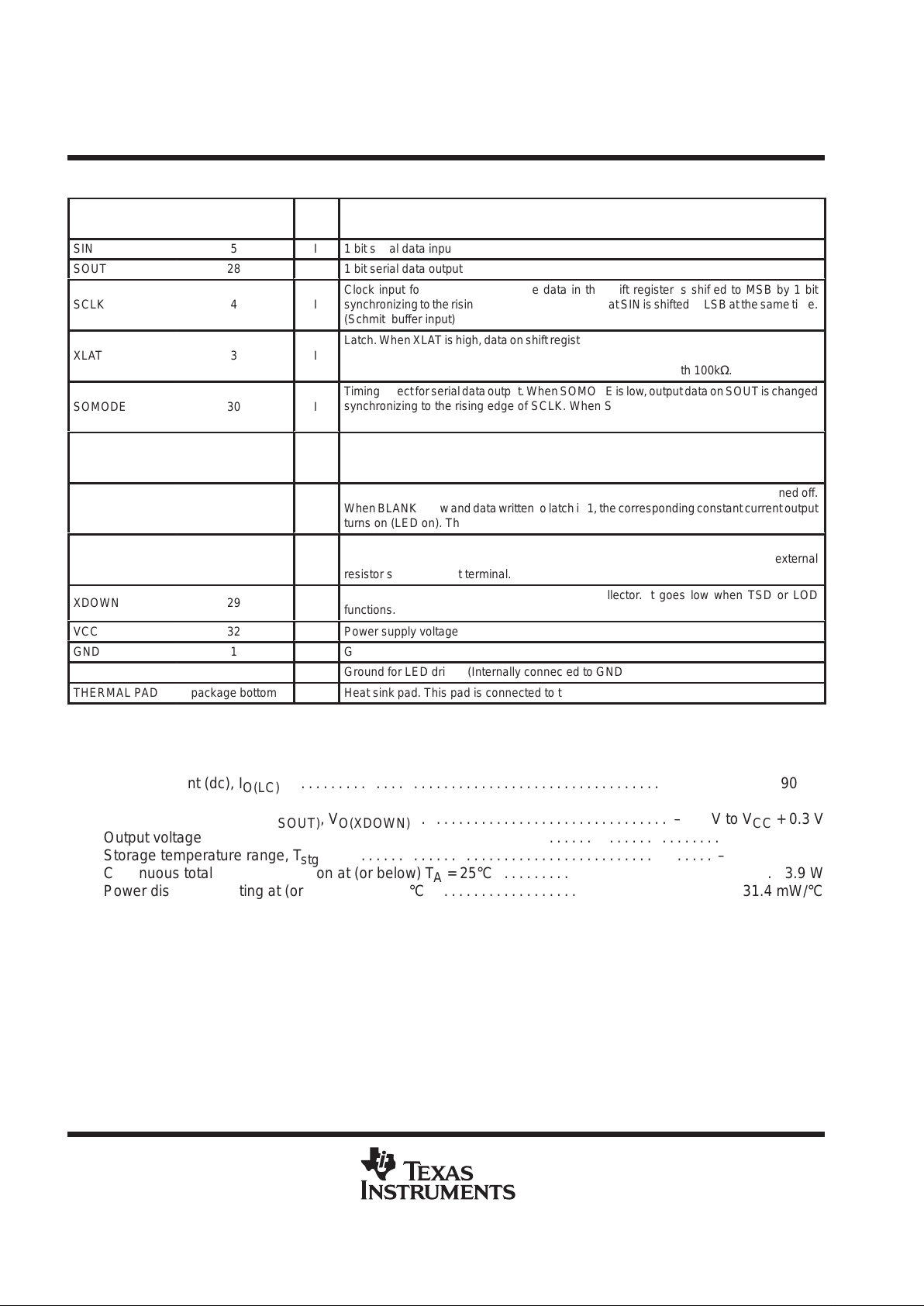
Terminal Functions
TERMINAL
NAME NO.
I/O
DESCRIPTION
SIN
5
I
1 bit serial data input
SOUT
28
O
1 bit serial data output
ÁÁÁÁ
Á
SCLK
ÁÁÁÁ
Á
4
Á
Á
I
ББББББББББББББББББББ
Á
Clock input for data transfer. All the data in the shift register is shifted to MSB by 1 bit
synchronizing to the rising edge of SCLK, and data at SIN is shifted to LSB at the same time.
(Schmitt buffer input)
ÁÁÁÁ
Á
ÁÁÁÁ
Á
XLAT
ÁÁÁÁ
Á
ÁÁÁÁ
Á
3
Á
Á
Á
Á
I
ББББББББББББББББББББ
Á
ББББББББББББББББББББ
Á
Latch. When XLAT is high, data on shift register goes through latch. When XLA T is low, data
is latched. Accordingly, if data on shift register is changed during XLA T high, this new value
is latched (level latch). This terminal is internally pulled down with 100kΩ.
ÁÁÁÁ
Á
SOMODE
ÁÁÁÁ
Á
30
Á
Á
I
ББББББББББББББББББББ
Á
Timing select for serial data output. When SOMODE is low , output data on SOUT is changed
synchronizing to the rising edge of SCLK. When SOMODE is high, output data on SOUT
is changed synchronizing to the falling edge of SCLK.
ÁÁÁÁ
Á
OUT0 – OUT15
ÁÁÁÁ
Á
7,8,10,1 1,12,13,
15,16,17,18,20,
21,22,23,25,26
Á
Á
O
ББББББББББББББББББББ
Á
Constant current output.
ÁÁÁÁ
Á
BLANK
ÁÁÁÁ
Á
2
Á
Á
I
ББББББББББББББББББББ
Á
Blank(Light off). When BLANK is high, all the output of constant current driver is turned off.
When BLANK is low and data written to latch is 1, the corresponding constant current output
turns on (LED on). This terminal is internally pulled up with 100kΩ.
ÁÁÁÁ
Á
IREF
ÁÁÁÁ
Á
31
Á
Á
I
ББББББББББББББББББББ
Á
Constant current value setting. LED current is set to desired value by connecting external
resistor between IREF and GND. The 38 times current compared to current across external
resistor sink on output terminal.
ÁÁÁÁ
Á
XDOWN
ÁÁÁÁ
Á
29
Á
Á
O
ББББББББББББББББББББ
Á
Error output. XDOWN is configured as open collector. It goes low when TSD or LOD
functions.
VCC
32
Power supply voltage
GND
1
Ground
PGND
6,9,14,19,24,27
Ground for LED driver. (Internally connected to GND)
THERMAL PAD
package bottom
Heat sink pad. This pad is connected to the lowest potential to IC or thermal layer.
absolute maximum ratings (see Note 1)
†
Supply voltage, VCC – 0.3 V to 7 V. . . . . . . . . . . . . . . . . . . . . . . . . . . . . . . . . . . . . . . . . . . . . . . . . . . . . . . . . . . . . . .
Output current (dc), I
O(LC)
90 mA. . . . . . . . . . . . . . . . . . . . . . . . . . . . . . . . . . . . . . . . . . . . . . . . . . . . . . . . . . . . . . . .
Input voltage range, VI – 0.3 V to V
CC
+ 0.3 V. . . . . . . . . . . . . . . . . . . . . . . . . . . . . . . . . . . . . . . . . . . . . . . . . . . . . .
Output voltage range, V
O(SOUT)
, V
O(XDOWN)
– 0.3 V to V
CC
+ 0.3 V. . . . . . . . . . . . . . . . . . . . . . . . . . . . . . . . .
Output voltage range, V
O(OUTn)
– 0.3 V to 18 V. . . . . . . . . . . . . . . . . . . . . . . . . . . . . . . . . . . . . . . . . . . . . . . . . . . .
Storage temperature range, T
stg
–40°C to 150°C. . . . . . . . . . . . . . . . . . . . . . . . . . . . . . . . . . . . . . . . . . . . . . . . . . .
Continuous total power dissipation at (or below) TA = 25°C 3.9 W. . . . . . . . . . . . . . . . . . . . . . . . . . . . . . . . . . . .
Power dissipation rating at (or above) TA = 25°C 31.4 mW/°C. . . . . . . . . . . . . . . . . . . . . . . . . . . . . . . . . . . . . . .
†
Stresses beyond those listed under “absolute maximum ratings” may cause permanent damage to the device. These are stress ratings only, and
functional operation of the device at these or any other conditions beyond those indicated under “recommended operating conditions” is not
implied. Exposure to absolute-maximum-rated conditions for extended periods may affect device reliability.
NOTE 1: All voltage values are with respect to GND terminal.
TLC5921
LED DRIVER
SLLS390 – SEPTEMBER 1999
5
POST OFFICE BOX 655303 • DALLAS, TEXAS 75265
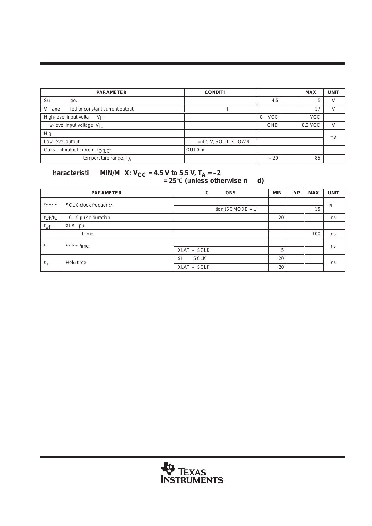
recommended operating conditions
dc characteristics
PARAMETER
CONDITIONS
MIN
NOM
MAX
UNIT
Supply voltage, V
CC
4.5
5
ÁÁÁ
5.5
V
Voltage applied to constant current output, V
O
OUT0 to OUT15 off
ÁÁÁ
17
V
High-level input voltage, V
IH
0.8 VCC
ÁÁÁ
VCC
V
Low-level input voltage, V
IL
GND
ÁÁÁ
0.2 VCC
V
High-level output current, I
OH
VCC = 4.5 V, SOUT
ÁÁÁ
–1
Low-level output current, I
OL
VCC = 4.5 V, SOUT, XDOWN
ÁÁÁ
1
mA
Constant output current, I
O(LC)
OUT0 to OUT15
ÁÁÁ
80
mA
Operating free-air temperature range, T
A
–20
ÁÁÁ
85
°C
ac characteristics, MIN/MAX: V
CC
= 4.5 V to 5.5 V, TA = –20 to 85°C
TYP: V
CC
= 5 V, TA = 25°C (unless otherwise noted)
PARAMETER
CONDITIONS
MIN
TYP
MAX
UNIT
At single operation
20
f
SCLK
SCLK clock frequenc
y
At cascade operation (SOMODE = L)
15
MH
z
twh/twlSCLK pulse duration
20
ns
t
wh
XLAT pulse duration
10
ns
tr/t
f
Rise/fall time
100
ns
p
SIN – SCLK
5
tsuSetup time
XLAT – SCLK
5
ns
SIN – SCLK
20
thHold time
XLAT – SCLK
20
ns

TLC5921
LED DRIVER
SLLS390 – SEPTEMBER 1999
6
POST OFFICE BOX 655303 • DALLAS, TEXAS 75265
electrical characteristics, MIN/MAX: V
CC
= 4.5 V to 5.5 V, T
A
= – 20 to 85°C
TYP: V
CC
= 5 V, T
A
= 25°C (unless otherwise noted)
PARAMETER
TEST CONDITIONS
MIN
TYP
MAX
UNIT
ÁÁÁ
Á
V
OH
БББББББББ
Á
High-level output voltage
ББББББББББ
Á
IOH = – 1 mA
Á
Á
V
CC
–0.5V
ÁÁÁÁÁ
Á
V
V
OL
Low-level output voltage
IOL = 1 mA
0.5
V
I
I
Input current
VI = VCC or GND (except BLANK, XLAT)
± 1
µA
ÁÁÁÁБББББББББÁББББББББББ
Á
Input signal is static, VO = 1 V,
R
(IREF)
= 10 kΩ, All output bits turn off
ÁÁÁ
Á
3
Á
Á
4.5
Á
Á
ÁÁÁÁБББББББББÁББББББББББ
Á
Input signal is static, VO = 1 V
R
IREF
= 1300 Ω, All output bits turn off
ÁÁÁ
Á
7
Á
Á
9
Á
Á
I
CC
Supply current
Input signal is static, VO = 1 V,
R
(IREF)
= 640 Ω, All output bits turn off
11
15
mA
ÁÁÁÁБББББББББÁББББББББББ
Á
Data transfer, VO = 1 V,
R
(IREF)
= 1300 Ω, All output bits turn on
ÁÁÁ
Á
15
Á
Á
20
Á
Á
Data transfer, VO = 1 V,
R
(IREF)
= 640 Ω, All output bits turn on
35
50
I
OL(C1)
Constant output current
VO = 1 V, R
(IREF)
= 1300 Ω
35
40
45
mA
I
OL(C2)
Constant output current
VO = 1 V R
(IREF)
= 640 Ω
70
80
90
mA
p
OUT0 to OUT15 (V
(OUTn)
= 15 V)
0.1
µA
I
lkg
Constant output leakage current
XDOWN (5V pullup)
1
µA
∆I
O(LC)
Constant output current error between bit
VO = 1 V, R
(IREF)
= 640 Ω,
All output bits turn on
± 1
± 4
%
ÁÁÁ
Á
I∆
O(LC1)
БББББББББ
Á
Changes in constant output current
depend on supply voltage
ББББББББББ
Á
V
ref
= 1.3 V
ÁÁÁ
Á
± 1
Á
Á
± 4
Á
Á
%/V
ÁÁÁ
Á
I∆
O(LC2)
БББББББББ
Á
Changes in constant output current
depend on output voltage
ББББББББББ
Á
VO = 1 V to 3 V , R
(IREF)
= 1300 Ω,
V
ref
= 1.3 V, 1 bit output turn on
ÁÁÁ
Á
± 2
Á
Á
± 6
Á
Á
%/V
T(
tsd)
TSD detection temperature
Junction temperature
150
160
170
°C
V
ref
Reference voltage
R
(IREF)
= 640 Ω
1.3
V
V
(LEDDET)
LED disconnection detection voltage
0.3
V
switching characteristics, CL = 15 pF
PARAMETER
TEST CONDITIONS
MIN
TYP
MAX
UNIT
SOUT
15
20
trRise time
OUTn (see Figure 1)
300
ns
SOUT
5
15
tfFall time
OUTn
300
ns
BLANK↑ – OUTn
400
650
BLANK↓ – OUTn
300
400
t
pd
Propagation delay time
BLANK↑ – XDOWN (see Note 2)
600
1000
ns
BLANK↓ – XDOWN (see Note 2)
500
1000
SCLK – SOUT
10
20
35
NOTE 2: At external resistor 5 kΩ

TLC5921
LED DRIVER
SLLS390 – SEPTEMBER 1999
7
POST OFFICE BOX 655303 • DALLAS, TEXAS 75265
PARAMETER MEASUREMENT INFORMATION
V
CC
IREF OUTn
GND
V
CC
51 Ω
15 pF
1300 Ω
Figure 1. Rise Time and Fall Time Test Circuit for OUTn
t
f
50%
t
r
90%
10%
VIH or V
OH
VIL or V
OL
100%
0%
VIH or V
OH
VIL or V
OL
50%
100%
0%
VIH or V
OH
VIL or V
OL
t
d1
t
wh
t
wl
50%
100%
0%
V
IH
V
IL
100%
0%
Figure 2. Timing Requirements

TLC5921
LED DRIVER
SLLS390 – SEPTEMBER 1999
8
POST OFFICE BOX 655303 • DALLAS, TEXAS 75265
PRINCIPLES OF OPERATION
setting for constant output current value
The constant current value is determined by external resistor, R
(IREF)
between IREF and GND. Refer constant
output current characteristics shown on Figure 5 for this external resistor value.
Note that more current flows if connect IREF to GND directly.
constant output current operation
When BLANK is low, the corresponding output is turned on if data latch value is 1, and turned off if data latch
value is 0. When BLANK is high, all outputs are forced to turn off. If there is constant current output terminal
left unconnected (includes LED disconnection), it should be lighted on after writing zero to corresponding data
latch to its output. If this operation is not done, supply current through constant current driver will increase.
shift register latch
The shift register latch is configured with 16 × 1 bits. The 1 bit for constant current output data represents ON
for constant current output if data is 1, or OFF if data is 0. The configuration of shift register latch is shown in
below.
(1 bits)
OUT15
Data
XLATCH
(1 bits)
OUT14
Data
(1 bits)
OUT1
Data
(1 bits)
OUT0
Data
Data Latch
16
SOUT
Shift Register
15 2 1
SIN
SCLK
Figure 3. Relationship Between Shift Register and Latch
SOUT output timing selection
By setting level of SOMODE, the SOUT output timing can be changed. When SOMODE is set to low, data is
clocked out to SOUT synchronized on the rising edge of SCLK, and when SOMODE is set to high, data is
clocked out to SOUT synchronized on the falling edge of SCLK. When SOMODE is set to high and shift
operation is done, the data shift error can be prevented even though SCLK signal is externally buffered in serial.
Note that the maximum data transfer rate in cascade operation is slower than that when SMODE is set to low.
TSD (thermal shutdown)
When the junction temperature exceeds the limit, TSD starts to function and turn constant current output off and
XDOWN goes low. Since XDOWN is configured with open-collector output, the outputs of multiple ICs can be
concatenated. To recover from constant current output off-state to normal operation, power supply should be
turned off and then turned on after several seconds.

TLC5921
LED DRIVER
SLLS390 – SEPTEMBER 1999
9
POST OFFICE BOX 655303 • DALLAS, TEXAS 75265
PRINCIPLES OF OPERATION
LOD function (LED open detection)
If any terminal voltage of constant current output (OUT0 TO 15) to be turned on is approximately below 0.3 V,
XDOWN output goes low during output on by knowing LED disconnection. This function is operational for
sixteen OUTn individually. To know which constant current output is disconnected, the level of XDOWN is
repeatedly checked 16 times from OUT0 to OUT15 turning one constant current output on. The power supply
voltage for LED should be set to that the constant current output is applied to above 0.4 V to prevent from
XDOWN low when LED is lighting on normally. Note that on-time should be minimum1µs after the constant
current output is turned on since XDOWN output is required approximately 1 µs.
As discussed earlier, XDOWN is used for both TSD and LOD function. Therefore, BLANK is used to know which
one of TSD or LOD worked when XDOWN went low at LED disconnection, that is, in this condition, when set
BLANK to high, all the constant current outputs are turned off and LOD disconnection detection is disabled, then,
if XDOWN was changed to high, LED disconnection must be occurred.
Table 1 is an example for XDOWN output status using four LEDs.
Table 1. XDOWN Output Example
LED NUMBER
1
2
3
ÁÁÁÁ
4
LED STATUS
GOOD
NG
GOOD
ÁÁÁÁ
NG
OUTn
ON
ON
ON
ÁÁÁÁ
ON
DETECTION RESULT
GOOD
NG
GOOD
ÁÁÁÁ
NG
XDOWN
LOW (by case 2, 4)
LED NUMBER
1
2
3
ÁÁÁÁ
4
LED STATUS
GOOD
NG
GOOD
ÁÁÁÁ
NG
OUTn
ON
ON
OFF
OFF
DETECTION RESULT
GOOD
NG
GOOD
ÁÁÁÁ
GOOD
XDOWN
LOW (by case 2)
LED NUMBER
1
2
3
ÁÁÁÁ
4
LED STATUS
GOOD
NG
GOOD
ÁÁÁÁ
NG
OUTn
OFF
OFF
OFF
ÁÁÁÁ
OFF
DETECTION RESULT
GOOD
GOOD
GOOD
ÁÁÁÁ
GOOD
XDOWN2
HIGH–IMPEDANCE
noise reduction : output slope
When output current is 80 mA, the time to change constant current output to turn-on and turn-off is approximately
150 ns and 250 ns respectively. This allows to reduce concurrent switching noise occurred when multiple
outputs turn or off at the same time.
thermal pad
The thermal pad should be connected to GND to eliminate the noise influence since it is connected to the bottom
side of IC chip. Also, desired thermal effect will be obtained by connecting this pad to the PCB pattern with better
thermal conductivity .

TLC5921
LED DRIVER
SLLS390 – SEPTEMBER 1999
10
POST OFFICE BOX 655303 • DALLAS, TEXAS 75265
PRINCIPLES OF OPERATION
power rating – free-air temperature
2.0
3.9
TA – Free–Air Temperature – °C
0 25 85–20
1.48
3.2
0
0
– Total Power Dissipation – WP
D
Output Voltage (Constant Current) – V
NOTES: A. The data is based on simulation result. When TI recommended print circuit board is used, derate linearly at the rate of 31.4mW/°C
for operation above 25°C free-air temperature. VCC=5 V , I
O(LC)
= 80 mA, ICC is typical value.
B. The thermal impedance will be varied depend on mounting conditions. Since PZP package established low thermal impedance by
radiating heat from thermal pad, the thermal pad should be soldered to pattern with low thermal impedance.
C. The material for PCB should be selected considering the thermal characteristics since the temperature will rise around the thermal
pad.
Figure 4. Power Rating

TLC5921
LED DRIVER
SLLS390 – SEPTEMBER 1999
11
POST OFFICE BOX 655303 • DALLAS, TEXAS 75265
PRINCIPLES OF OPERATION
constant output current
500
I
lkg
– Input Leakage Current – (mA)
100000
1000
10 20 30 40 60 70 80
100
10000
66000
13200
6000
2750
1800
1300
860
1040
730
640
Conditions : VO = 1 V, V
ref
= 1.3 V
NOTE: The resistor, R
(IREF)
, should be located as close to IREF terminal as possible to avoid the noise influence.
R
(ref)
Ω()
– Reference Resistance –
Figure 5. Current on Constant Current Output vs External Resistor

TLC5921
LED DRIVER
SLLS390 – SEPTEMBER 1999
Template Release Date: 7–11–94
12
POST OFFICE BOX 655303 DALLAS, TEXAS 75265
•
SD15_A
BLANK
XLAT
SCLK
SOMODE
SOUT
OUTn
XDOWN
SIN
1/f
SCLK
SD14_A
td (SCLK–SOUT)
Figure 6. Timing Diagram
SD00_B SD01_B SD02_B SD14_B SD15_B SD00_DSD15_CSD14_CSD00_C
tsu (SIN–SCLK) th (SIN–SCLK)
tsu (XLAT–SCLK)
twl (SCLK) twh (SCLK)
td (SCLK–SOUT)
td (SCLK–SOUT)
SD15_A SD00_B SD01_B SD14_B SD15_B SD00_C
DRIVER OFFDRIVER OFF
td (BLANK–OUTn)
td (BLANK–OUTn)
DRIVER ONDRIVER ON DRIVER OFFDRIVER OFF
td (BLANK–XDOWN)
td (BLANK–XDOWN)
(Note)
NOTE : LED disconnected
SD01_A SD02_A
HI–Z
SD00_A
th (XLAT–SCLK)

TLC5921
LED DRIVER
SLLS390 – SEPTEMBER 1999
13
POST OFFICE BOX 655303 • DALLAS, TEXAS 75265
MECHANICAL DATA
DAP (R-PDSO-G**) PowerPAD PLASTIC SMALL-OUTLINE PACKAGE
0,25
0,75
0,50
0,15 NOM
Gage Plane
NOM
6,20
8,40
7,80
Thermal Pad
(see Note D)
38
12,60
11,10
32
Seating Plane
12,4010,90
4073257/A 07/97
20
0,19
19
A
0,30
38
1
9,80
28
A MAX
PINS **
9,60
A MIN
DIM
1,20 MAX
10,90
11,10
30
38 PINS SHOWN
0,10
0,65
M
0,13
0°–8°
0,15
0,05
NOTES: A. All linear dimensions are in millimeters.
B. This drawing is subject to change without notice.
C. Body dimensions do not include mold flash or protrusion.
D. The package thermal performance may be enhanced by bonding the thermal pad to an external thermal plane.
This pad is electrically and thermally connected to the backside of the die and possibly selected leads.
E. Falls within JEDEC MO-153
PowerPAD is a trademark of Texas Instruments Incorporated.

IMPORTANT NOTICE
T exas Instruments and its subsidiaries (TI) reserve the right to make changes to their products or to discontinue
any product or service without notice, and advise customers to obtain the latest version of relevant information
to verify, before placing orders, that information being relied on is current and complete. All products are sold
subject to the terms and conditions of sale supplied at the time of order acknowledgement, including those
pertaining to warranty, patent infringement, and limitation of liability.
TI warrants performance of its semiconductor products to the specifications applicable at the time of sale in
accordance with TI’s standard warranty. Testing and other quality control techniques are utilized to the extent
TI deems necessary to support this warranty. Specific testing of all parameters of each device is not necessarily
performed, except those mandated by government requirements.
CERT AIN APPLICATIONS USING SEMICONDUCTOR PRODUCTS MAY INVOLVE POTENTIAL RISKS OF
DEATH, PERSONAL INJURY, OR SEVERE PROPERTY OR ENVIRONMENTAL DAMAGE (“CRITICAL
APPLICATIONS”). TI SEMICONDUCTOR PRODUCTS ARE NOT DESIGNED, AUTHORIZED, OR
WARRANTED TO BE SUITABLE FOR USE IN LIFE-SUPPORT DEVICES OR SYSTEMS OR OTHER
CRITICAL APPLICATIONS. INCLUSION OF TI PRODUCTS IN SUCH APPLICA TIONS IS UNDERSTOOD T O
BE FULLY AT THE CUSTOMER’S RISK.
In order to minimize risks associated with the customer’s applications, adequate design and operating
safeguards must be provided by the customer to minimize inherent or procedural hazards.
TI assumes no liability for applications assistance or customer product design. TI does not warrant or represent
that any license, either express or implied, is granted under any patent right, copyright, mask work right, or other
intellectual property right of TI covering or relating to any combination, machine, or process in which such
semiconductor products or services might be or are used. TI’s publication of information regarding any third
party’s products or services does not constitute TI’s approval, warranty or endorsement thereof.
Copyright 1999, Texas Instruments Incorporated
 Loading...