

TLC5920
16x8 BIT LED DRIVER/CONTROLLER
SLAS264 – MARCH 2000
1
POST OFFICE BOX 655303 • DALLAS, TEXAS 75265
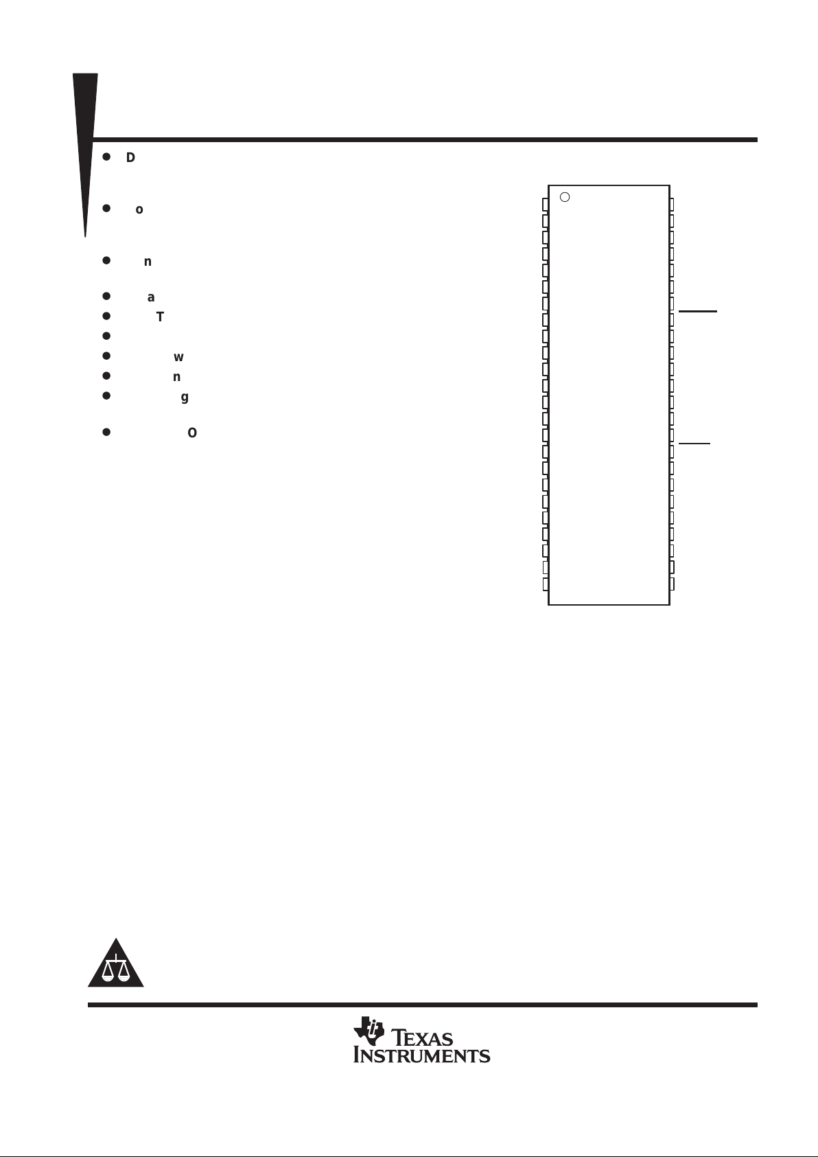
D
Drive Capability:
– Segment . . . 30 mA × 16 Bits
– Common . . . 640 mA
D
Constant Current Output ...3 mA to 30 mA
(Current Value Setting for All Channels
Using External Resistor)
D
Constant Current Accuracy ±6% (Maximum
Error Between Bits)
D
Data Input: Clock Synchronized Serial Input
D
LED Type Applied Cathode Common
D
Logic Power Supply Voltage 4.5 V to 5.5 V
D
LED Power Supply Voltage 4.5 V to 5.5 V
D
Operating Frequency . . . 10 MHz
D
Operating Free-Air Temperature Range
–20°C to 85°C
D
48-Pin SSOL Package
description
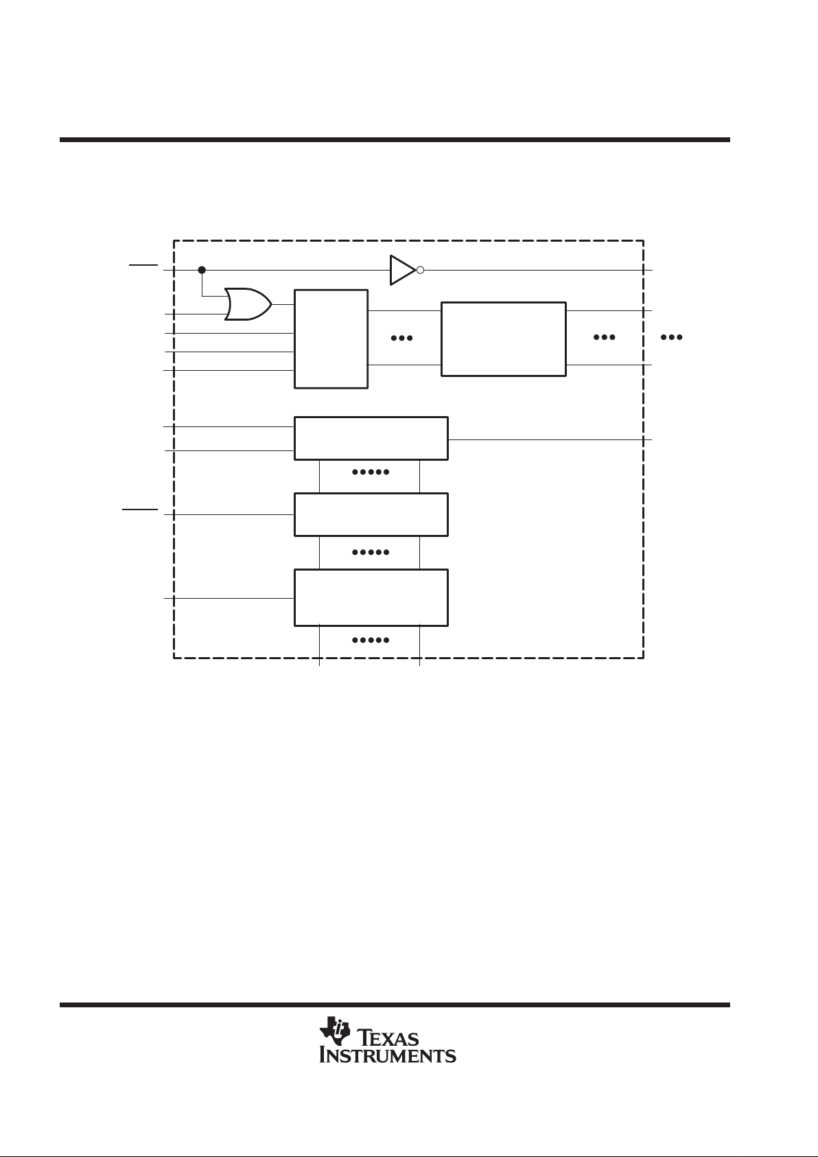
The TLC5920 is an LED driver incorporating a
16-channel shift register, data latch, and constant
current circuitry with current value control and
8-channel common driver into a single chip. The
constant output current is capable of 30 mA for 16
bits simultaneously , and the current value can be
set by one external register. This device also
includes a 16-bit segment driver and 8-bit
common driver; therefore, the monocolor LED
array with 16 × 8 dots can be driven by only one
TLC5920, and a two-color LED array with 16 x 16
dots can be driven by two TLC5920s.
Copyright 2000, Texas Instruments Incorporated
PRODUCTION DATA information is current as of publication date.
Products conform to specifications per the terms of Texas Instruments
standard warranty. Production processing does not necessarily include
testing of all parameters.
Please be aware that an important notice concerning availability, standard warranty, and use in critical applications of
Texas Instruments semiconductor products and disclaimers thereto appears at the end of this data sheet.
1
2
3
4
5
6
7
8
9
10
11
12
13
14
15
16
17
18
19
20
21
22
23
24
48
47
46
45
44
43
42
41
40
39
38
37
36
35
34
33
32
31
30
29
28
27
26
25
COM3
COM2
COM1
COM0
GNDLED
NC
NC
VLED
S0
S1
S2
S3
S4
S5
S6
S7
IREF
VLED
VANA
NC
GNDANA
S8
S9
S10
GNDLED
COM4
COM5
COM6
COM7
GNDLED
SIN
LATCH
SCLK
BLANK
CSEL0
GNDLOG
CSEL1
CSEL2
VLOG
DSEL
SOUT
VLED
DSEL
S15
S14
S13
S12
S11
DL PACKAGE
(TOP VIEW)
TLC5920
16x8 BIT LED DRIVER/CONTROLLER
SLAS264 – MARCH 2000
2
POST OFFICE BOX 655303 • DALLAS, TEXAS 75265
functional block diagram
S15
Common
Driver
3 TO 8
Decoder
S0
16 bits
Shift Register
16 bits
Data Latch
Segment Driver
and
Current Control
DSEL
BLANK
CSEL0
CSEL1
CSEL2
SIN
SCLK
LATCH
IREF
DSEL
COM0
COM7
SOUT
TLC5920
16x8 BIT LED DRIVER/CONTROLLER
SLAS264 – MARCH 2000
3
POST OFFICE BOX 655303 • DALLAS, TEXAS 75265
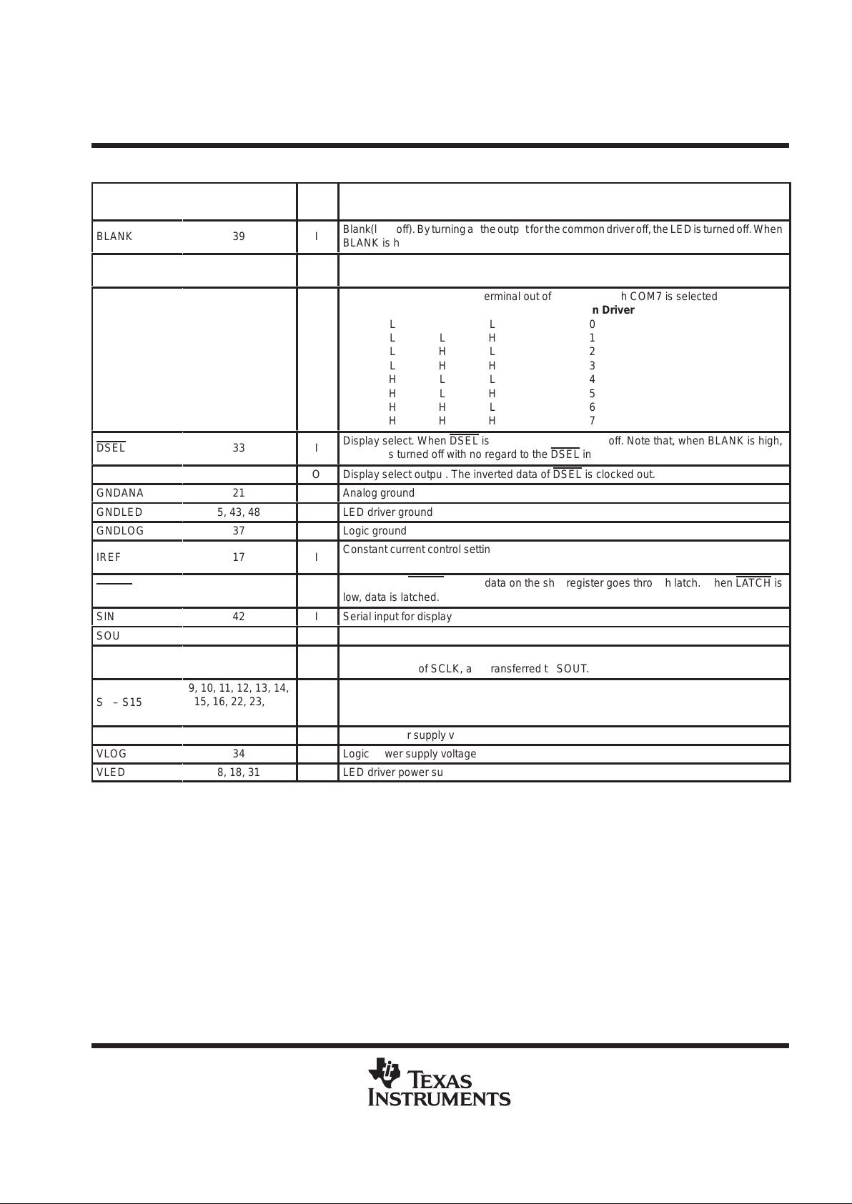
Terminal Functions
TERMINAL
NAME NO.
I/O
DESCRIPTION
ÁÁÁ
Á
BLANK
ÁÁÁÁ
Á
39
Á
Á
I
ББББББББББББББББББББ
Á
Blank(light off). By turning all the output for the common driver off, the LED is turned off. When
BLANK is high, the LED is turned off.
ÁÁÁ
Á
COM0 – COM7
ÁÁÁÁ
Á
4, 3, 2, 1, 47, 46,
45, 44
Á
Á
O
ББББББББББББББББББББ
Á
LED common driver output
ÁÁÁ
Á
ÁÁÁ
Á
ÁÁÁ
Á
ÁÁÁ
Á
ÁÁÁ
Á
CSEL0 – 2
ÁÁÁÁ
Á
ÁÁÁÁ
Á
ÁÁÁÁ
Á
ÁÁÁÁ
Á
ÁÁÁÁ
Á
38, 36, 35
Á
Á
Á
Á
Á
Á
Á
Á
Á
Á
I
ББББББББББББББББББББ
Á
ББББББББББББББББББББ
Á
ББББББББББББББББББББ
Á
ББББББББББББББББББББ
Á
ББББББББББББББББББББ
Á
Common driver select. One terminal out of COM0 through COM7 is selected.
2 1 0 Common Driver
LLL 0
LLH 1
LHL 2
LHH 3
HLL 4
HLH 5
HHL 6
HHH 7
ÁÁÁ
Á
DSEL
ÁÁÁÁ
Á
33
Á
Á
I
ББББББББББББББББББББ
Á
Display select. When DSEL is high, the LED is turned off. Note that, when BLANK is high,
the LED is turned off with no regard to the DSEL
input.
DSEL
30
O
Display select output. The inverted data of DSEL is clocked out.
GNDANA
21
Analog ground
GNDLED
5, 43, 48
LED driver ground
GNDLOG
37
Logic ground
ÁÁÁ
Á
IREF
ÁÁÁÁ
Á
17
Á
Á
I
ББББББББББББББББББББ
Á
Constant current control setting. The LED current is set to the desired value by connecting
an external resistor between IREF and GND.
ÁÁÁ
Á
LATCH
ÁÁÁÁ
Á
41
Á
Á
I
ББББББББББББББББББББ
Á
Latch. When LATCH is high, data on the shift register goes through latch. When LATCH is
low, data is latched.
SIN
42
I
Serial input for display
SOUT
32
O
Serial output for display
ÁÁÁ
Á
SCLK
ÁÁÁÁ
Á
40
Á
Á
I
ББББББББББББББББББББ
Á
Synchronous clock input for serial data transfer. The input data of SIN is synchronized to
the rising edge of SCLK, and transferred to SOUT.
ÁÁÁ
Á
S0 – S15
ÁÁÁÁ
Á
9, 10, 11, 12, 13, 14,
15, 16, 22, 23, 24,
25, 26, 27, 28, 29
Á
Á
O
ББББББББББББББББББББ
Á
LED segment driver output
VANA
19
Analog power supply voltage
VLOG
34
Logic power supply voltage
VLED
8, 18, 31
LED driver power supply voltage
TLC5920
16x8 BIT LED DRIVER/CONTROLLER
SLAS264 – MARCH 2000
4
POST OFFICE BOX 655303 • DALLAS, TEXAS 75265
absolute maximum ratings† (see Note 1)
Logic supply voltage, V
(LOG)
– 0.3 V to 7 V. . . . . . . . . . . . . . . . . . . . . . . . . . . . . . . . . . . . . . . . . . . . . . . . . . . . . . . .
LED supply voltage, V
(LED)
– 0.3 V to 7 V. . . . . . . . . . . . . . . . . . . . . . . . . . . . . . . . . . . . . . . . . . . . . . . . . . . . . . . . .
Analog supply voltage, V
(ANA)
– 0.3 V to 7 V. . . . . . . . . . . . . . . . . . . . . . . . . . . . . . . . . . . . . . . . . . . . . . . . . . . . . . .
Output current, I
OH(S)
– 32 mA. . . . . . . . . . . . . . . . . . . . . . . . . . . . . . . . . . . . . . . . . . . . . . . . . . . . . . . . . . . . . . . . . .
Output current, I
OL(C)
650 mA. . . . . . . . . . . . . . . . . . . . . . . . . . . . . . . . . . . . . . . . . . . . . . . . . . . . . . . . . . . . . . . . . . .
Input voltage range, VI – 0.3 V to V
(LOG)
+ 0.3 V. . . . . . . . . . . . . . . . . . . . . . . . . . . . . . . . . . . . . . . . . . . . . . . . . . . .
Output voltage range, VO – 0.3 V to V
(LOG)
+ 0.3 V. . . . . . . . . . . . . . . . . . . . . . . . . . . . . . . . . . . . . . . . . . . . . . . . .
Continuous total power dissipation 1500 mW. . . . . . . . . . . . . . . . . . . . . . . . . . . . . . . . . . . . . . . . . . . . . . . . . . . . . .
Thermal resistance 83°C/W. . . . . . . . . . . . . . . . . . . . . . . . . . . . . . . . . . . . . . . . . . . . . . . . . . . . . . . . . . . . . . . . . . . . . .
Operating free-air temperature range (see Note 2), T
A
– 20 to 85°C. . . . . . . . . . . . . . . . . . . . . . . . . . . . . . . . . . .
Storage temperature range, T
stg
–40°C to 125°C. . . . . . . . . . . . . . . . . . . . . . . . . . . . . . . . . . . . . . . . . . . . . . . . . . .
†
Stresses beyond those listed under “absolute maximum ratings” may cause permanent damage to the device. These are stress ratings only, and
functional operation of the device at these or any other conditions beyond those indicated under “recommended operating conditions” is not
implied. Exposure to absolute-maximum-rated conditions for extended periods may affect device reliability.
NOTES: 1. All voltage values are with respect to GND terminal.
2. TJ ≤ 150°C (refer to appendix thermal condition).
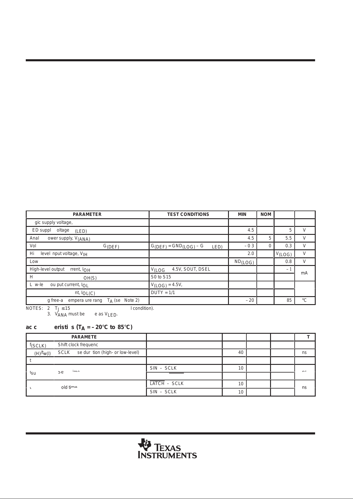
recommended operating conditions
dc characteristics (see Note 3)
PARAMETER
TEST CONDITIONS
MIN
NOM
MAX
UNIT
Logic supply voltage, V
(LOG)
4.5
5
5.5
V
LED supply voltage, V
(LED)
4.5
5
5.5
V
Analog power supply, V
(ANA)
4.5
5
5.5
V
Voltage between GND and V
(DEF), G(DEF)
G
(DEF)
= GND
(LOG)
– GND
(LED)
–0.3
0
0.3
V
High-level input voltage, V
IH
2.0
V
(LOG)
V
Low-level input voltage, V
IL
GND
(LOG)
0.8
V
High-level output current, I
OH
V
(LOG)
= 4.5V, SOUT, DSEL
–1
High-level output current, I
OH(S)
S0 to S15
–30
mA
Low-level output current, I
OL
V
(LOG)
= 4.5V, SOUT, DSEL
1.6
Low-level output current, I
OL(C)
DUTY = 1/16, COM0 to COM7
640
mA
Operating free-air temperature range, TA (see Note 2)
–20
85
°C
NOTES: 2 TJ ≤ 150°C (refer to appendix thermal condition).
3. V
ANA
must be same as V
LED
.
ac characteristics (TA = –20°C to 85°C)
PARAMETER
TEST CONDITIONS
MIN
NOM
MAX
UNIT
f
(SCLK)
Shift clock frequency
10
MHz
t
w(H)/tw(l)
SCLK pulse duration (high- or low-level)
40
ns
tr/t
f
Rise/fall time
100
ns
p
SIN – SCLK
10
tsuSetup time
SCLK – LATCH
10
ns
LATCH – SCLK
10
thHold time
SIN – SCLK
10
ns
TLC5920
16x8 BIT LED DRIVER/CONTROLLER
SLAS264 – MARCH 2000
5
POST OFFICE BOX 655303 • DALLAS, TEXAS 75265
electrical characteristics (unless otherwise noted),
MIN/MAX: V
(LOG)
= V
(ANA)
= V
(LED)
= 4.5 V to 5.5 V, T
A
= –20°C to 85°C
TYP: V
(LOG)
= V
(ANA)
= V
(LED)
= 5 V, T
A
= 25°C
PARAMETER
TEST CONDITIONS
MIN
TYP
MAX
UNIT
V
OH
High-level output voltage
IOH = –1 mA, SOUT, DSEL
3.6
V
p
IOL = 1.6 mA, SOUT , DSEL
0.6
VOLLow-level output voltage
IOL = 640 mA, COM0 to COM7
0.6
0.9
V
I
I
Input current
VI = V
(LOG)
or GND
(LOG)
±1
µA
I
(LOG)
Data transfer, SCLK = 10 MHz
0.1
I
(LED)
Supply current
LED is turned off
0.8
1.6
mA
I
(ANA)
LED is turned off
0.8
1.6
I
OH(S03)
V
(Sn)
= 2.5 V , R
(IREF)
= 4200 Ω
–2.45
–3
–3.45
I
OH(S10)
V
(Sn)
= 2.5 V , R
(IREF)
= 1260 Ω
–8.5
–10
–11.5
I
OH(S20)
Segment current
V
(Sn)
= 2.5 V , R
(IREF)
= 630 Ω
–17
–20
–23
mA
I
OH(S30)
V
(Sn)
= 2.5 V , R
(IREF)
= 420 Ω
–25.5
–30
–34.5
ÁÁ
Á
∆I
OH(S)
БББББББББББ
Á
Segment current error between bits
ББББББББ
Á
V
(LED)
= 5 V, R
(IREF)
= 630 Ω,
V
(Sn)
= 2.5 V
ÁÁÁ
Á
±3%
Á
Á
±6%
Á
Á
V
REF
Voltage reference
1.2
1.26
1.3
V
switching characteristics, CL = 15 pF
PARAMETER
TEST CONDITIONS
MIN
TYP
MAX
UNIT
SOUT
40
DSEL
40
trRise time
COMn
80
ns
Sn
80
SOUT
40
DSEL
40
tfFall time
COMn
40
ns
Sn
40
LATCH –Sn
40
p
SCLK – Sn
40
tdPropagation delay time
SCLK – SOUT
40
ns
DSEL – DSEL
40
CSELn – COMn
120
t
(DLH)
Propagation delay time
DSEL – COMn
120
ns
()
BLANK – COMn
120
CSELn – COMn
40
t
(DHL)
Propagation delay time
DSEL – COMn
40
ns
()
BLANK – COMn
40
TLC5920
16x8 BIT LED DRIVER/CONTROLLER
SLAS264 – MARCH 2000
6
POST OFFICE BOX 655303 • DALLAS, TEXAS 75265
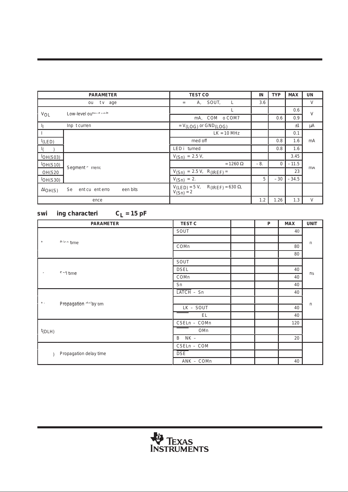
PARAMETER MEASUREMENT INFORMATION
0.78
1.5
TA – Free-Air Temperature – °C
0 25 85–20
POWER RATING
vs
FREE-AIR TEMPERATURE
–
I
Power Rating
– mAI
OH(S)
I
OH(S)
+
V
REF
R
(IREF)
10
0
R
(IREF)
– kΩ
2.50.5
10
20
30
40
1 1.5 2 30
VCC = 5 V,
V
(Sn)
= 2.5 V,
TA = 25°C
SEGMENT CURRENT – I
OHS
Segment Current –
TLC5920
16x8 BIT LED DRIVER/CONTROLLER
SLAS264 – MARCH 2000
POST OFFICE BOX 655303 DALLAS, TEXAS 75265
• 7
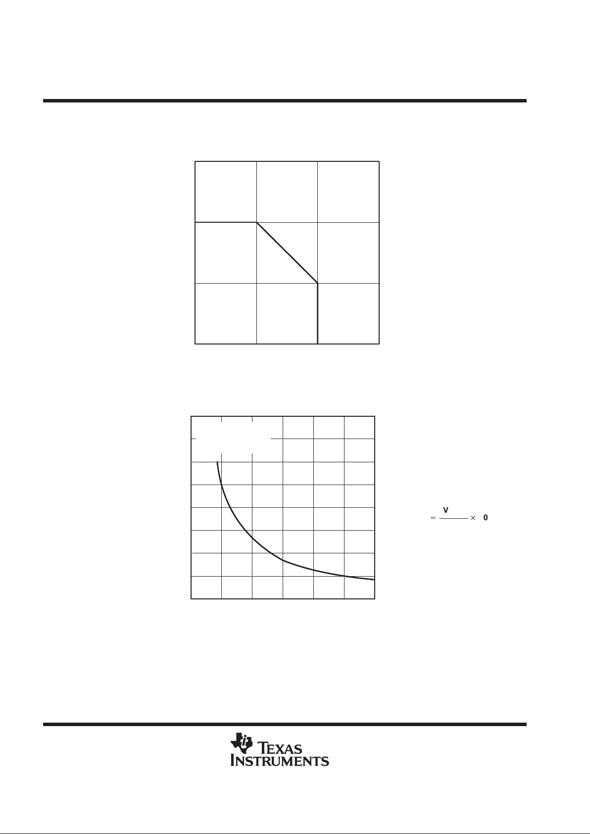
timing diagram (common driver)
CSEL0
tsu BLK–CSEL
th BLK–CSEL
td DSEL
CSEL1
CSEL2
DSEL
BLANK
COM0
COM1
COM2
COM3
COM4
COM5
COM6
COM7
DSEL
td BLK–COMMON
td BLK–COMMON
td DSEL–COMMON
Segment Data Write Timing

TLC5920
16x8 BIT LED DRIVER/CONTROLLER
SLAS264 – MARCH 2000
Template Release Date: 7–11–94
8
POST OFFICE BOX 655303 DALLAS, TEXAS 75265
•
timing diagram (segment driver)
D0A D14AD1A D2A D0B D01B D2BD15A
D0B D1B D2B
D1B D2B D3B
D14B D15B D0C
D15B D0C D1C
D14B
D15BD14BD14A D15A
SCLK
tsu D–CLK
D0A D1A D2A D0B D1B D2B D0C D1C D2C
D15A D15A
D13BD14A D14A
D0BD1A D1A
SIN
LATCH
S14
S15
D15AD0A D0A
th(LAT–SCLK)
tsu(LAT–SCLK)
th D–CLK
t
clk
t
wl
t
wh
t
r
td LAT–SO
td SCLK–SO
td SCLK–SOUT
S0
S1
SOUT
t
f
tw LAT
TLC5920
16x8 BIT LED DRIVER/CONTROLLER
SLAS264 – MARCH 2000
9
POST OFFICE BOX 655303 • DALLAS, TEXAS 75265
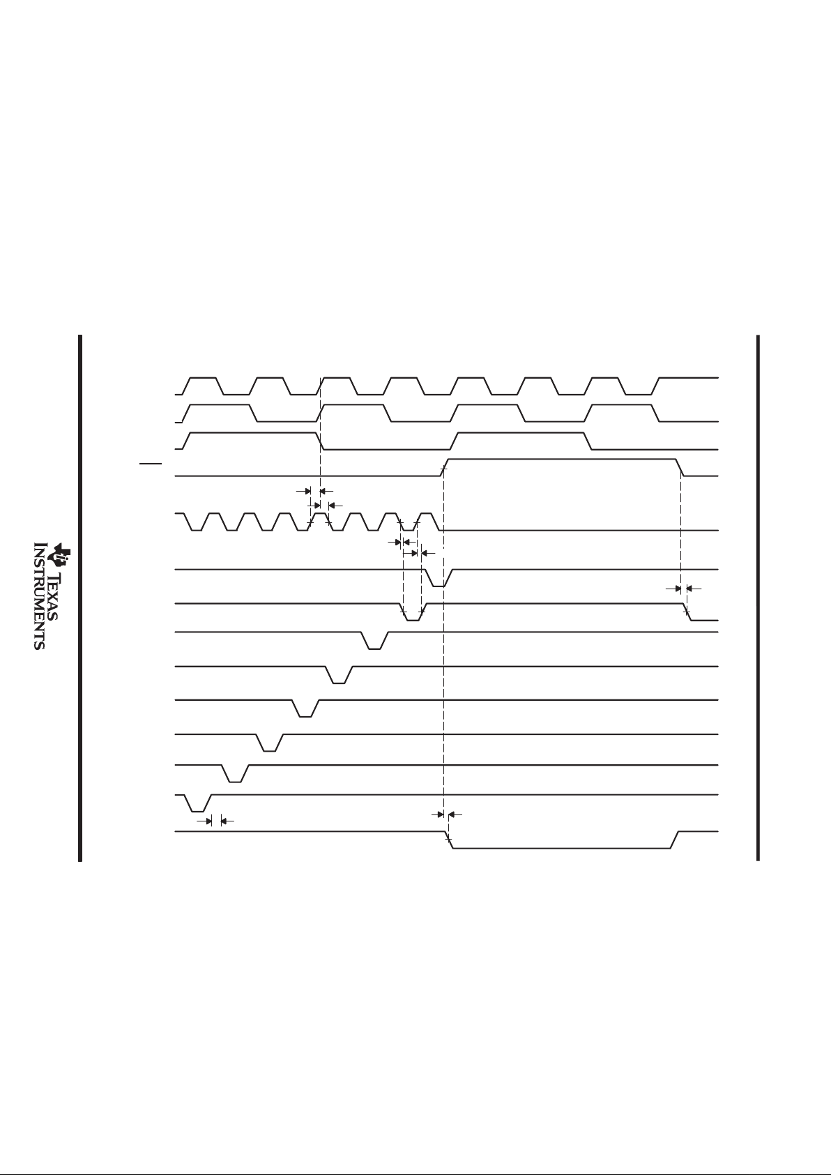
APPLICATION INFORMATION
example 1
The other remaining terminals used for dot matrix LED drive can be utilized for LED lamp drive and other
displays.
LEDs driven by TLC5920
cathode common type
LED
TLC5920
DRIVE CURRENT
TYPE
NO. OF COLOR
QUANTITY
QUANTITY
DUTY
(mA)
Mono
16
1
Static
30
LAMP
Two
8
1
Static
30
Mono
16
1
1/8
30
7 SEGMENT
Two
8
1
1/8
30
Mono
3
1
1/8
30
5
x
7
Two
1
1
1/8
30
Mono
2
1
1/8
30
8
x
8
Two
1
1
1/8
30
Mono
2
2
1/16
20
16 x 16
Two
1
2
1/16
20
Three
1
3
1/16
13
Mono
2
3
1/24
13
24
x
24
Two
1
3
1/24
13
TLC5920
S15
COM0
COM6
COM7
S14 S10 S9 S5 S4 S0
= LED

TLC5920
16x8 BIT LED DRIVER/CONTROLLER
SLAS264 – MARCH 2000
10
POST OFFICE BOX 655303 • DALLAS, TEXAS 75265
APPLICATION INFORMATION
example 2
Using two TLC5920s, an LED with two colors and 16 x 16 dots can be driven. The number of LED arrays can
also be increased by making a cascade connection in the application circuit.
COM7
IREF
IC2
TLC5920
DSEL
SCLKSCLK
DSEL
SIN
DSEL
COM0
COM7
IC1
TLC5920
2SOUT
Red
SIN
SOUT
2DSEL
2IREF
SOUT
DSEL
IREF
COM0
1SOUT
Green
1IREF
1SIN
Green
2SIN
Red
1DSEL
SCLK
LATCH
BLANK
CSEL2
CSEL0
CSEL1
S15
S0
16 x 16 Dots
Two–Colors LED Array
S15
S0
CSEL0
CSEL1
CSEL2
BLANK
LATCH
CSEL0
CSEL1
CSEL2
BLANK
LATCH
= LED
TLC5920
16x8 BIT LED DRIVER/CONTROLLER
SLAS264 – MARCH 2000
11
POST OFFICE BOX 655303 • DALLAS, TEXAS 75265
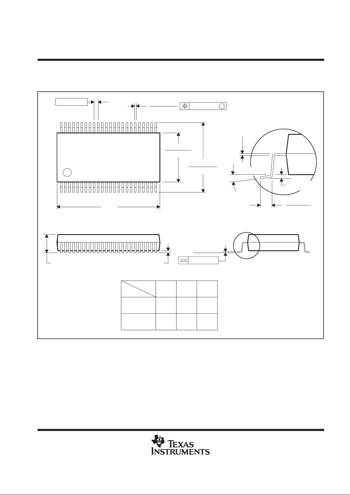
MECHANICAL DATA
DL (R-PDSO-G**) PLASTIC SMALL-OUTLINE PACKAGE
4040048/D 08/97
48 PINS SHOWN
56
0.730
(18,54)
0.720
(18,29)
4828
0.370
(9,40)
(9,65)
0.380
Gage Plane
DIM
0.420 (10,67)
0.395 (10,03)
A MIN
A MAX
0.006 (0,15) NOM
PINS **
0.630
(16,00)
(15,75)
0.620
0.010 (0,25)
Seating Plane
0.020 (0,51)
0.040 (1,02)
25
24
0.008 (0,203)
0.012 (0,305)
48
1
0.008 (0,20) MIN
A
0.110 (2,79) MAX
0.299 (7,59)
0.291 (7,39)
0.004 (0,10)
M
0.005 (0,13)
0.025 (0,635)
0°–8°
NOTES: A. All linear dimensions are in inches (millimeters).
B. This drawing is subject to change without notice.
C. Body dimensions do not include mold flash or protrusion not to exceed 0.006 (0,15).
D. Falls within JEDEC MO-118

IMPORTANT NOTICE
T exas Instruments and its subsidiaries (TI) reserve the right to make changes to their products or to discontinue
any product or service without notice, and advise customers to obtain the latest version of relevant information
to verify, before placing orders, that information being relied on is current and complete. All products are sold
subject to the terms and conditions of sale supplied at the time of order acknowledgement, including those
pertaining to warranty, patent infringement, and limitation of liability.
TI warrants performance of its semiconductor products to the specifications applicable at the time of sale in
accordance with TI’s standard warranty. Testing and other quality control techniques are utilized to the extent
TI deems necessary to support this warranty. Specific testing of all parameters of each device is not necessarily
performed, except those mandated by government requirements.
CERT AIN APPLICATIONS USING SEMICONDUCTOR PRODUCTS MAY INVOLVE POTENTIAL RISKS OF
DEATH, PERSONAL INJURY, OR SEVERE PROPERTY OR ENVIRONMENTAL DAMAGE (“CRITICAL
APPLICATIONS”). TI SEMICONDUCTOR PRODUCTS ARE NOT DESIGNED, AUTHORIZED, OR
WARRANTED TO BE SUITABLE FOR USE IN LIFE-SUPPORT DEVICES OR SYSTEMS OR OTHER
CRITICAL APPLICATIONS. INCLUSION OF TI PRODUCTS IN SUCH APPLICA TIONS IS UNDERSTOOD T O
BE FULLY AT THE CUSTOMER’S RISK.
In order to minimize risks associated with the customer’s applications, adequate design and operating
safeguards must be provided by the customer to minimize inherent or procedural hazards.
TI assumes no liability for applications assistance or customer product design. TI does not warrant or represent
that any license, either express or implied, is granted under any patent right, copyright, mask work right, or other
intellectual property right of TI covering or relating to any combination, machine, or process in which such
semiconductor products or services might be or are used. TI’s publication of information regarding any third
party’s products or services does not constitute TI’s approval, warranty or endorsement thereof.
Copyright 2000, Texas Instruments Incorporated
 Loading...