

Page 1
TLC5920
16x8 BIT LED DRIVER/CONTROLLER
SLAS264A – MARCH 2000 REVISED SEPTEMBER 2002
D
Drive Capability:
– Segment . . . 30 mA × 16 Bits
– Common . . . 640 mA
D
Constant Current Output ...3 mA to 30 mA
(Current Value Setting for All Channels
Using External Resistor)
D
Constant Current Accuracy ±6% (Maximum
Error Between Bits)
D
Data Input: Clock Synchronized Serial Input
D
LED Type Applied Cathode Common
D
Logic Power Supply Voltage 4.5 V to 5.5 V
D
LED Power Supply Voltage 4.5 V to 5.5 V
D
Operating Frequency . . . 10 MHz
D
Operating Free-Air Temperature Range
–20°C to 85°C
D
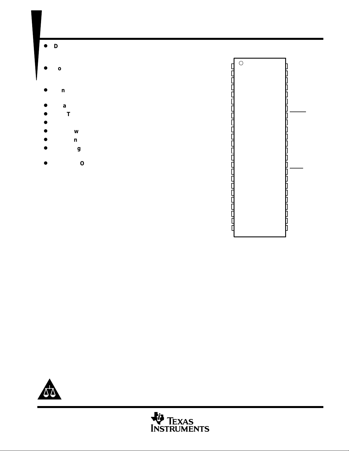
48-Pin SSOL Package
description
The TLC5920 is an LED driver incorporating a
16-channel shift register, data latch, and constant
current circuitry with current value control and
8-channel common driver into a single chip. The
constant output current is capable of 30 mA for 16
bits simultaneously , and the current value can be
set by one external register. This device also
includes a 16-bit segment driver and 8-bit
common driver; therefore, the monocolor LED
array with 16 × 8 dots can be driven by only one
TLC5920, and a two-color LED array with 16 x 16
dots can be driven by two TLC5920s.
COM3
COM2
COM1
COM0
GNDLED
NC
NC
VLED
S0
S1
S2
S3
S4
S5
S6
S7
IREF
VLED
VANA
NC
GNDANA
S8
S9
S10
DL PACKAGE
(TOP VIEW)
1
2
3
4
5
6
7
8
9
10
11
12
13
14
15
16
17
18
19
20
21
22
23
24
48
47
46
45
44
43
42
41
40
39
38
37
36
35
34
33
32
31
30
29
28
27
26
25
GNDLED
COM4
COM5
COM6
COM7
GNDLED
SIN
LATCH
SCLK
BLANK
CSEL0
GNDLOG
CSEL1
CSEL2
VLOG
DSEL
SOUT
VLED
DSEL
S15
S14
S13
S12
S11
Please be aware that an important notice concerning availability, standard warranty, and use in critical applications of
Texas Instruments semiconductor products and disclaimers thereto appears at the end of this data sheet.
PRODUCTION DATA information is current as of publication date.
Products conform to specifications per the terms of Texas Instruments
standard warranty. Production processing does not necessarily include
testing of all parameters.
POST OFFICE BOX 655303 • DALLAS, TEXAS 75265
Copyright 2002, Texas Instruments Incorporated
1
Page 2
TLC5920
16x8 BIT LED DRIVER/CONTROLLER
SLAS264A – MARCH 2000 REVISED SEPTEMBER 2002
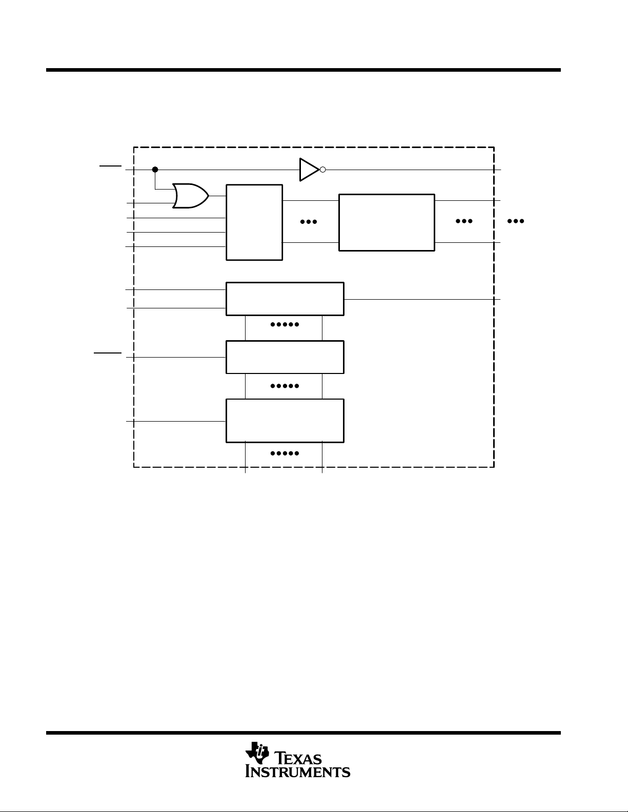
functional block diagram
DSEL
BLANK
CSEL0
CSEL1
CSEL2
SIN
SCLK
LATCH
IREF
3 TO 8
Decoder
16 bits
Shift Register
16 bits
Data Latch
Segment Driver
Current Control
DSEL
COM0
Common
Driver
COM7
SOUT
and
S0
S15
2
POST OFFICE BOX 655303 • DALLAS, TEXAS 75265
Page 3
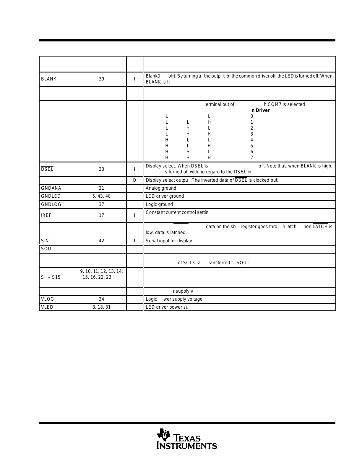
I/O
DESCRIPTION
Á
Á
Á
Á
Á
Á
Á
Á
Á
Á
Á
Á
Á
Á
Á
Á
Á
Á
Á
Á
Á
Á
Á
Á
Á
Á
Á
Á
Á
Á
Á
Á
Á
Á
Á
Á
Á
Á
Á
Á
Á
Á
Á
Á
Á
Á
Á
Á
TERMINAL
NAME NO.
BLANK
ÁÁÁ
COM0 – COM7
ÁÁÁ
ÁÁÁ
ÁÁÁ
CSEL0 – 2
ÁÁÁ
ÁÁÁ
ÁÁÁ
DSEL
ÁÁÁ
DSEL
GNDANA
GNDLED
GNDLOG
IREF
ÁÁÁ
LATCH
ÁÁÁ
SIN
SOUT
SCLK
ÁÁÁ
S0 – S15
ÁÁÁ
VANA
VLOG
VLED
39
ÁÁÁÁ
4, 3, 2, 1, 47, 46,
45, 44
ÁÁÁÁ
ÁÁÁÁ
ÁÁÁÁ
38, 36, 35
ÁÁÁÁ
ÁÁÁÁ
ÁÁÁÁ
33
ÁÁÁÁ
30
21
5, 43, 48
37
17
ÁÁÁÁ
41
ÁÁÁÁ
42
32
40
ÁÁÁÁ
9, 10, 11, 12, 13, 14,
15, 16, 22, 23, 24,
ÁÁÁÁ
25, 26, 27, 28, 29
19
34
8, 18, 31
Á
Á
Á
Á
Á
Á
Á
Á
Á
Á
Á
Á
16x8 BIT LED DRIVER/CONTROLLER
SLAS264A – MARCH 2000 REVISED SEPTEMBER 2002
Terminal Functions
Blank(light off). By turning all the output for the common driver off, the LED is turned off. When
I
ББББББББББББББББББББ
BLANK is high, the LED is turned off.
O
LED common driver output
ББББББББББББББББББББ
Common driver select. One terminal out of COM0 through COM7 is selected.
2 1 0 Common Driver
ББББББББББББББББББББ
ББББББББББББББББББББ
I
ББББББББББББББББББББ
ББББББББББББББББББББ
ББББББББББББББББББББ
Display select. When DSEL is high, the LED is turned off. Note that, when BLANK is high,
I
ББББББББББББББББББББ
the LED is turned off with no regard to the DSEL
O
Display select output. The inverted data of DSEL is clocked out.
Analog ground
LED driver ground
Logic ground
Constant current control setting. The LED current is set to the desired value by connecting
I
ББББББББББББББББББББ
an external resistor between IREF and GND.
Latch. When LATCH is high, data on the shift register goes through latch. When LATCH is
I
low, data is latched.
ББББББББББББББББББББ
I
Serial input for display
O
Serial output for display
Synchronous clock input for serial data transfer. The input data of SIN is synchronized to
I
ББББББББББББББББББББ
the rising edge of SCLK, and transferred to SOUT.
O
LED segment driver output
ББББББББББББББББББББ
Analog power supply voltage
Logic power supply voltage
LED driver power supply voltage
LLL 0
LLH 1
LHL 2
LHH 3
HLL 4
HLH 5
HHL 6
HHH 7
input.
TLC5920
POST OFFICE BOX 655303 • DALLAS, TEXAS 75265
3
Page 4
TLC5920
mA
mA
tsuSetup time
ns
thHold time
ns
16x8 BIT LED DRIVER/CONTROLLER
SLAS264A – MARCH 2000 REVISED SEPTEMBER 2002
absolute maximum ratings† (see Note 1)
Logic supply voltage, V
LED supply voltage, V
Analog supply voltage, V
Output current, I
Output current, I
OH(S)
650 mA. . . . . . . . . . . . . . . . . . . . . . . . . . . . . . . . . . . . . . . . . . . . . . . . . . . . . . . . . . . . . . . . . . .
OL(C)
Input voltage range, V
Output voltage range, V
– 0.3 V to 7 V. . . . . . . . . . . . . . . . . . . . . . . . . . . . . . . . . . . . . . . . . . . . . . . . . . . . . . . .
(LOG)
– 0.3 V to 7 V. . . . . . . . . . . . . . . . . . . . . . . . . . . . . . . . . . . . . . . . . . . . . . . . . . . . . . . . .
(LED)
– 0.3 V to 7 V. . . . . . . . . . . . . . . . . . . . . . . . . . . . . . . . . . . . . . . . . . . . . . . . . . . . . . .
(ANA)
– 32 mA. . . . . . . . . . . . . . . . . . . . . . . . . . . . . . . . . . . . . . . . . . . . . . . . . . . . . . . . . . . . . . . . . .
– 0.3 V to V
I
– 0.3 V to V
O
(LOG)
(LOG)
+ 0.3 V. . . . . . . . . . . . . . . . . . . . . . . . . . . . . . . . . . . . . . . . . . . . . . . . . . . .
+ 0.3 V. . . . . . . . . . . . . . . . . . . . . . . . . . . . . . . . . . . . . . . . . . . . . . . . .
Continuous total power dissipation 1500 mW. . . . . . . . . . . . . . . . . . . . . . . . . . . . . . . . . . . . . . . . . . . . . . . . . . . . . .
Thermal resistance 83°C/W. . . . . . . . . . . . . . . . . . . . . . . . . . . . . . . . . . . . . . . . . . . . . . . . . . . . . . . . . . . . . . . . . . . . . .
Operating free-air temperature range (see Note 2), T
Storage temperature range, T
†
Stresses beyond those listed under “absolute maximum ratings” may cause permanent damage to the device. These are stress ratings only, and
functional operation of the device at these or any other conditions beyond those indicated under “recommended operating conditions” is not
implied. Exposure to absolute-maximum-rated conditions for extended periods may affect device reliability.
NOTES: 1. All voltage values are with respect to GND terminal.
2. TJ ≤ 150°C (refer to appendix thermal condition).
–40°C to 125°C. . . . . . . . . . . . . . . . . . . . . . . . . . . . . . . . . . . . . . . . . . . . . . . . . . .
stg
– 20 to 85°C. . . . . . . . . . . . . . . . . . . . . . . . . . . . . . . . . . .
A
recommended operating conditions
dc characteristics (see Note 3)
PARAMETER
Logic supply voltage, V
LED supply voltage, V
Analog power supply, V
Voltage between GND and V
High-level input voltage, V
Low-level input voltage, V
High-level output current, I
High-level output current, I
Low-level output current, I
Low-level output current, I
Operating free-air temperature range, TA (see Note 2)
NOTES: 2 TJ ≤ 150°C (refer to appendix thermal condition).
3. V
ANA
(LOG)
(LED)
(ANA)
(DEF), G(DEF)
IH
IL
OH
OH(S)
OL
OL(C)
must be same as V
LED
.
TEST CONDITIONS
G
= GND
(DEF)
V
= 4.5V, SOUT, DSEL
(LOG)
S0 to S15
V
= 4.5V, SOUT, DSEL
(LOG)
DUTY = 1/16, COM0 to COM7
(LOG)
– GND
(LED)
GND
MIN
(LOG)
4.5
4.5
4.5
–0.3
2.0
–20
NOM
MAX
5
5
5
0
V
(LOG)
5.5
5.5
5.5
0.3
0.8
–1
–30
1.6
640
85
UNIT
V
V
V
V
V
V
°C
ac characteristics (TA = –20°C to 85°C)
PARAMETER
f
(SCLK)
t
w(H)/tw(l)
tr/t
f
4
Shift clock frequency
SCLK pulse duration (high- or low-level)
Rise/fall time
p
POST OFFICE BOX 655303 • DALLAS, TEXAS 75265
TEST CONDITIONS
SIN – SCLK
SCLK – LATCH
LATCH – SCLK
SIN – SCLK
MIN
40
10
10
10
10
NOM
MAX
10
100
UNIT
MHz
ns
ns
Page 5

VOLLow-level output voltage
V
Segment current
mA
Á
Á
Á
Á
Á
Á
trRise time
ns
tfFall time
ns
tdPropagation delay time
ns
(
)
()
(
)
()
electrical characteristics (unless otherwise noted),
MIN/MAX: V
TYP: V
(LOG)
(LOG)
= V
= V
(ANA)
(ANA)
= V
= V
(LED)
= 5 V, TA = 25°C
(LED)
= 4.5 V to 5.5 V, T
16x8 BIT LED DRIVER/CONTROLLER
SLAS264A – MARCH 2000 REVISED SEPTEMBER 2002
= –20°C to 85°C
A
TLC5920
PARAMETER
V
OH
High-level output voltage
p
I
I
I
(LOG)
I
(LED)
I
(ANA)
I
OH(S03)
I
OH(S10)
I
OH(S20)
I
OH(S30)
∆I
OH(S)
ÁÁ
V
REF
Input current
Supply current
Segment current error between bits
БББББББББББ
Voltage reference
switching characteristics, CL = 15 pF
PARAMETER
p
t
t
Propagation delay time
DLH
Propagation delay time
DHL
TEST CONDITIONS
IOH = –1 mA, SOUT, DSEL
IOL = 1.6 mA, SOUT, DSEL
IOL = 640 mA, COM0 to COM7
VI = V
(LOG)
or GND
(LOG)
Data transfer, SCLK = 10 MHz
LED is turned off
LED is turned off
V
= 2.5 V , R
(Sn)
V
= 2.5 V , R
(Sn)
V
= 2.5 V , R
(Sn)
V
= 2.5 V , R
(Sn)
V
= 5 V, R
(LED)
V
= 2.5 V
(Sn)
ББББББББ
(IREF)
(IREF)
(IREF)
(IREF)
(IREF)
= 4200 Ω
= 1260 Ω
= 630 Ω
= 420 Ω
= 630 Ω,
TEST CONDITIONS
SOUT
DSEL
COMn
Sn
SOUT
DSEL
COMn
Sn
LATCH – Sn
SCLK – Sn
SCLK – SOUT
DSEL – DSEL
CSELn – COMn
DSEL – COMn
BLANK – COMn
CSELn – COMn
DSEL – COMn
BLANK – COMn
MIN
MIN
TYP
3.6
–2.1
–8.5
–17
–25.5
1.2
±3%
1.26
ÁÁÁ
TYP
0.6
0.8
0.8
–3
–10
–20
–30
MAX
–3.9
–11.5
–34.5
Á
MAX
0.6
0.9
±1
0.1
1.6
1.6
–23
±6%
1.3
40
40
80
80
40
40
40
40
40
40
40
40
120
120
120
40
40
40
UNIT
V
µA
mA
Á
V
UNIT
ns
ns
POST OFFICE BOX 655303 • DALLAS, TEXAS 75265
5
Page 6

TLC5920
16x8 BIT LED DRIVER/CONTROLLER
SLAS264A – MARCH 2000 REVISED SEPTEMBER 2002
PARAMETER MEASUREMENT INFORMATION
FREE-AIR TEMPERATURE
1.5
–
Power Rating
I
0.78
POWER RATING
vs
– mAI
OH(S)
Segment Current –
40
30
20
10
0
0 25 85–20
TA – Free-Air Temperature – °C
SEGMENT CURRENT – I
VCC = 5 V,
V
= 2.5 V,
(Sn)
TA = 25°C
1 1.5 2 30
R
(IREF)
– kΩ
OHS
V
I
OH(S)
2.50.5
REF
+
R
(IREF)
10
6
POST OFFICE BOX 655303 • DALLAS, TEXAS 75265
Page 7

POST OFFICE BOX 655303 DALLAS, TEXAS 75265
timing diagram (common driver)
CSEL0
CSEL1
CSEL2
DSEL
tsu BLK–CSEL
th BLK–CSEL
BLANK
td BLK–COMMON
COM0
• 7
COM1
COM2
COM3
COM4
COM5
COM6
COM7
Segment Data Write Timing
DSEL
td BLK–COMMON
td DSEL
td DSEL–COMMON
16x8 BIT LED DRIVER/CONTROLLER
SLAS264A – MARCH 2000 REVISED SEPTEMBER 2002
TLC5920
Page 8

T
l
R
l
D
7
11
94
8
timing diagram (segment driver)
SCLK
tsu D–CLK
SIN
D0A D1A D2A D0B D1B D2B D0C D1C D2C
th D–CLK
th(LAT–SCLK)
t
clk
t
wl
t
wh
tsu(LAT–SCLK)
t
f
t
r
D15BD14BD14A D15A
SLAS264A – MARCH 2000 REVISED SEPTEMBER 2002
emp
ate
e
ease
ate:
TLC5920
16x8 BIT LED DRIVER/CONTROLLER
POST OFFICE BOX 655303 DALLAS, TEXAS 75265
•
LATCH
S0
S1
S14
S15
SOUT
td SCLK–SOUT
tw LAT
td LAT–SO
D15A D15A
D0A D14AD1A D2A D0B D01B D2BD15A
D14B
D13BD14A D14A
D0BD1A D1A
D15AD0A D0A
td SCLK–SO
D15B D0C D1C
D14B D15B D0C
D1B D2B D3B
D0B D1B D2B
–
–
Page 9

DUTY
LAMP
7 SEGMENT
5 x 7
8 x 8
24 x 24
16x8 BIT LED DRIVER/CONTROLLER
SLAS264A – MARCH 2000 REVISED SEPTEMBER 2002
APPLICATION INFORMATION
example 1
The other remaining terminals used for dot matrix LED drive can be utilized for LED lamp drive and other
displays.
LEDs driven by TLC5920
cathode common type
TYPE
16 x 16
LED
NO. OF COLOR
Mono
Two
Mono
Two
Mono
Two
Mono
Two
Mono
Two
Three
Mono
Two
QUANTITY
16
8
16
8
3
1
2
1
2
1
1
2
1
TLC5920
QUANTITY
1
1
1
1
1
1
1
1
2
2
3
3
3
Static
Static
1/8
1/8
1/8
1/8
1/8
1/8
1/16
1/16
1/16
1/24
1/24
DRIVE CURRENT
(mA)
30
30
30
30
30
30
30
30
20
20
13
13
13
TLC5920
S15
= LED
COM7
COM6
TLC5920
COM0
S14 S10 S9 S5 S4 S0
POST OFFICE BOX 655303 • DALLAS, TEXAS 75265
9
Page 10

TLC5920
16x8 BIT LED DRIVER/CONTROLLER
SLAS264A – MARCH 2000 REVISED SEPTEMBER 2002
APPLICATION INFORMATION
example 2
Using two TLC5920s, an LED with two colors and 16 x 16 dots can be driven. The number of LED arrays can
also be increased by making a cascade connection in the application circuit.
1IREF
1SOUT
Green
CSEL0
CSEL1
CSEL2
BLANK
LATCH
SCLK
1DSEL
2SIN
Red
2SOUT
Red
2DSEL
2IREF
16 x 16 Dots
Two–Colors LED Array
SOUT
DSEL
IREF
= LED
S15
CSEL0
CSEL1
TLC5920
IC2
CSEL2
BLANK
LATCH
DSEL
COM7
COM0
S0
SIN
SOUT
DSEL
IREF
S15
CSEL0
CSEL1
TLC5920
IC1
CSEL2
BLANK
LATCH
COM7
COM0
S0
SIN
SCLKSCLK
DSEL
1SIN
Green
10
POST OFFICE BOX 655303 • DALLAS, TEXAS 75265
Page 11

TLC5920
16x8 BIT LED DRIVER/CONTROLLER
SLAS264A – MARCH 2000 REVISED SEPTEMBER 2002
MECHANICAL DATA
DL (R-PDSO-G**) PLASTIC SMALL-OUTLINE PACKAGE
48 PINS SHOWN
0.025 (0,635)
48
1
0.110 (2,79) MAX
0.0135 (0,343)
0.008 (0,203)
25
0.299 (7,59)
0.291 (7,39)
24
A
0.008 (0,20) MIN
0.005 (0,13)
0.420 (10,67)
0.395 (10,03)
Seating Plane
0.004 (0,10)
M
0.010 (0,25)
0.005 (0,13)
Gage Plane
0.010 (0,25)
0°–8°
0.040 (1,02)
0.020 (0,51)
PINS **
DIM
A MAX
A MIN
NOTES: A. All linear dimensions are in inches (millimeters).
B. This drawing is subject to change without notice.
C. Body dimensions do not include mold flash or protrusion not to exceed 0.006 (0,15).
D. Falls within JEDEC MO-118
0.380
(9,65)
0.370
(9,40)
4828
0.630
(16,00)
0.620
(15,75)
56
0.730
(18,54)
0.720
(18,29)
4040048/E 12/01
POST OFFICE BOX 655303 • DALLAS, TEXAS 75265
11
Page 12

PACKAGE OPTION ADDENDUM
www.ti.com
27-Feb-2006
PACKAGING INFORMATION
Orderable Device Status
(1)
Package
Type
Package
Drawing
Pins Package
Qty
Eco Plan
TLC5920DL ACTIVE SSOP DL 48 25 Green (RoHS &
no Sb/Br)
TLC5920DLG4 ACTIVE SSOP DL 48 25 Green (RoHS &
no Sb/Br)
TLC5920DLR ACTIVE SSOP DL 48 1000 Green (RoHS &
no Sb/Br)
TLC5920DLRG4 ACTIVE SSOP DL 48 1000 Green (RoHS &
no Sb/Br)
(1)
The marketing status values are defined as follows:
ACTIVE: Product device recommended for new designs.
LIFEBUY: TI has announced that the device will be discontinued, and a lifetime-buy period is in effect.
NRND: Not recommended for new designs. Device is in production to support existing customers, but TI does not recommend using this part in
a new design.
PREVIEW: Device has been announced but is not in production. Samples may or may not be available.
OBSOLETE: TI has discontinued the production of the device.
(2)
Eco Plan - The planned eco-friendly classification: Pb-Free (RoHS), Pb-Free (RoHS Exempt), or Green (RoHS & no Sb/Br) - please check
http://www.ti.com/productcontent for the latest availability information and additional product content details.
TBD: The Pb-Free/Green conversion plan has not been defined.
Pb-Free (RoHS): TI's terms "Lead-Free" or "Pb-Free" mean semiconductor products that are compatible with the current RoHS requirements
for all 6 substances, including the requirement that lead not exceed 0.1% by weight in homogeneous materials. Where designed to be soldered
at high temperatures, TI Pb-Free products are suitable for use in specified lead-free processes.
Pb-Free (RoHS Exempt): This component has a RoHS exemption for either 1) lead-based flip-chip solder bumps used between the die and
package, or 2) lead-based die adhesive used between the die and leadframe. The component is otherwise considered Pb-Free (RoHS
compatible) as defined above.
Green (RoHS & no Sb/Br): TI defines "Green" to mean Pb-Free (RoHS compatible), and free of Bromine (Br) and Antimony (Sb) based flame
retardants (Br or Sb do not exceed 0.1% by weight in homogeneous material)
(2)
Lead/Ball Finish MSL Peak Temp
CU NIPDAU Level-2-260C-1 YEAR
CU NIPDAU Level-2-260C-1 YEAR
CU NIPDAU Level-2-260C-1 YEAR
CU NIPDAU Level-2-260C-1 YEAR
(3)
(3)
MSL, Peak Temp. -- The Moisture Sensitivity Level rating according to the JEDEC industry standard classifications, and peak solder
temperature.
Important Information and Disclaimer:The information provided on this page represents TI's knowledge and belief as of the date that it is
provided. TI bases its knowledge and belief on information provided by third parties, and makes no representation or warranty as to the
accuracy of such information. Efforts are underway to better integrate information from third parties. TI has taken and continues to take
reasonable steps to provide representative and accurate information but may not have conducted destructive testing or chemical analysis on
incoming materials and chemicals. TI and TI suppliers consider certain information to be proprietary, and thus CAS numbers and other limited
information may not be available for release.
In no event shall TI's liability arising out of such information exceed the total purchase price of the TI part(s) at issue in this document sold by TI
to Customer on an annual basis.
Addendum-Page 1
Page 13

IMPORTANT NOTICE
Texas Instruments Incorporated and its subsidiaries (TI) reserve the right to make corrections, modifications,
enhancements, improvements, and other changes to its products and services at any time and to discontinue
any product or service without notice. Customers should obtain the latest relevant information before placing
orders and should verify that such information is current and complete. All products are sold subject to TI’s terms
and conditions of sale supplied at the time of order acknowledgment.
TI warrants performance of its hardware products to the specifications applicable at the time of sale in
accordance with TI’s standard warranty. Testing and other quality control techniques are used to the extent TI
deems necessary to support this warranty. Except where mandated by government requirements, testing of all
parameters of each product is not necessarily performed.
TI assumes no liability for applications assistance or customer product design. Customers are responsible for
their products and applications using TI components. To minimize the risks associated with customer products
and applications, customers should provide adequate design and operating safeguards.
TI does not warrant or represent that any license, either express or implied, is granted under any TI patent right,
copyright, mask work right, or other TI intellectual property right relating to any combination, machine, or process
in which TI products or services are used. Information published by TI regarding third-party products or services
does not constitute a license from TI to use such products or services or a warranty or endorsement thereof.
Use of such information may require a license from a third party under the patents or other intellectual property
of the third party, or a license from TI under the patents or other intellectual property of TI.
Reproduction of information in TI data books or data sheets is permissible only if reproduction is without
alteration and is accompanied by all associated warranties, conditions, limitations, and notices. Reproduction
of this information with alteration is an unfair and deceptive business practice. TI is not responsible or liable for
such altered documentation.
Resale of TI products or services with statements different from or beyond the parameters stated by TI for that
product or service voids all express and any implied warranties for the associated TI product or service and
is an unfair and deceptive business practice. TI is not responsible or liable for any such statements.
Following are URLs where you can obtain information on other Texas Instruments products and application
solutions:
Products Applications
Amplifiers amplifier.ti.com Audio www.ti.com/audio
Data Converters dataconverter.ti.com Automotive www.ti.com/automotive
DSP dsp.ti.com Broadband www.ti.com/broadband
Interface interface.ti.com Digital Control www.ti.com/digitalcontrol
Logic logic.ti.com Military www.ti.com/military
Power Mgmt power.ti.com Optical Networking www.ti.com/opticalnetwork
Microcontrollers microcontroller.ti.com Security www.ti.com/security
Telephony www.ti.com/telephony
Video & Imaging www.ti.com/video
Wireless www.ti.com/wireless
Mailing Address: Texas Instruments
Post Office Box 655303 Dallas, Texas 75265
Copyright 2006, Texas Instruments Incorporated
 Loading...