

Page 1
TLC59025
www.ti.com
...................................................................................................................................................................................................... SLVS934 – JUNE 2009
LOW-POWER 16-CHANNEL CONSTANT-CURRENT LED SINK DRIVER
1
FEATURES
• 16 Constant-Current Output Channels • Schmitt-Trigger Inputs
• Matches Industry Standard IOUT to External • 3.3-V to 5-V Supply Voltage
Resistor Ratio
• Constant Output Current Invariant to Load Protection
Voltage Change
• Excellent Output Current Accuracy:
– Between Channels: < ± 5% (Max)
– Between ICs: < ± 6% (Max)
• Constant Output Current Range:
3 mA to 45 mA
• Output Current Adjusted By External Resistor
• Fast Response of Output Current, OE (Min):
100 ns
• 30-MHz Clock Frequency
DESCRIPTION/ORDERING INFORMATION
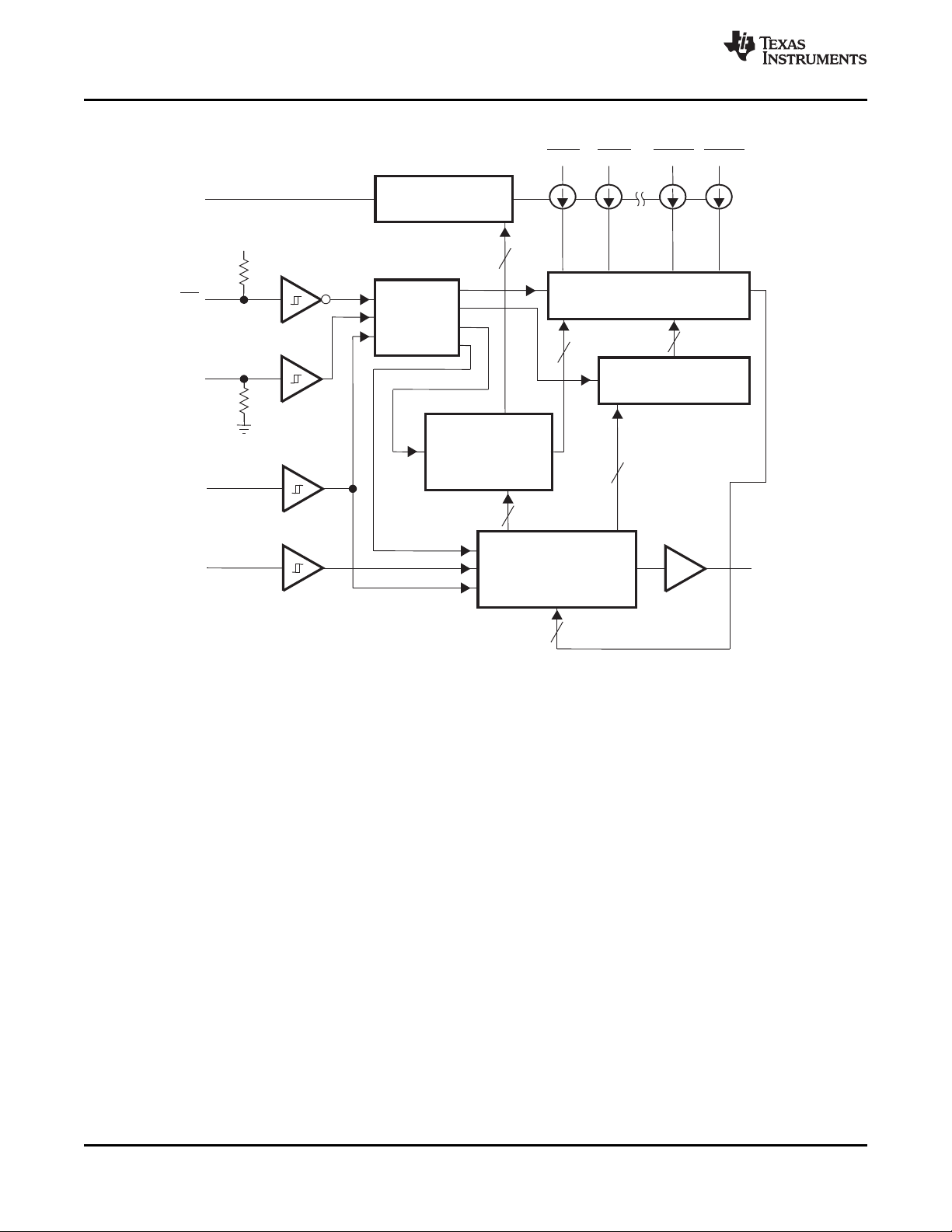
The TLC59025 is designed for LED displays and LED lighting applications. The TLC59025 contains a 16-bit shift
register and data latches, which convert serial input data into parallel output format. At the TLC59025 output
stage, 16 regulated-current ports provide uniform and constant current for driving LEDs within a wide range of VF
variations. Used in system design for LED display applications (e.g., LED panels), the TLC59025 provides great
flexibility and device performance. Users can adjust the output current from 3 mA to 45 mA through an external
resistor, R
at the output port. The high clock frequency, 30 MHz, also satisfies the system requirements of high-volume data
transmission.
, which gives flexibility in controlling the light intensity of LEDs. TLC59025 is designed for up to 17 V
ext
• Thermal Shutdown for Overtemperature
• ESD Performance: 1-kV HBM
APPLICATIONS
• Gaming Machine / Entertainment
• General LED Applications
• LED Display Systems
• Signs LED Lighting
• White Goods
The serial data is transferred into TLC59025 via SDI, shifted in the shift register, and transferred out via SDO. LE
can latch the serial data in the shift register to the output latch. OE enables the output drivers to sink current.
ORDERING INFORMATION
T
A
PW Reel of 2000 TLC59025IPWR PREVIEW
– 40 ° C to 85 ° C W-SOIC – DW Reel of 2000 TLC59025IDWR PREVIEW
SSOP – DBQ Reel of 2000 TLC59025IDBQR TLC59025
(1) For the most current package and ordering information, see the Package Option Addendum at the end of this document, or see the TI
web site at www.ti.com .
(2) Package drawings, thermal data, and symbolization are available at www.ti.com/packaging .
1
Please be aware that an important notice concerning availability, standard warranty, and use in critical applications of Texas
Instruments semiconductor products and disclaimers thereto appears at the end of this data sheet.
PRODUCTION DATA information is current as of publication date.
Products conform to specifications per the terms of the Texas
Instruments standard warranty. Production processing does not
necessarily include testing of all parameters.
PACKAGE
(2)
ORDERABLE PART NUMBER TOP-SIDE MARKING
(1)
Copyright © 2009, Texas Instruments Incorporated
Page 2
SDO
VDD
R-EXT
OE
LE
CLK
SDI
CONTROL
LOGIC
I/O REGULATOR
CONFIGURATION
LATCHES
OUTPUT DRIVER
16-BIT SHIFT
REGISTER
8
16
8
16
16
16
OUT15
OUT14OUT0 OUT1
16-BIT OUTPUT
LATCH
TLC59025
SLVS934 – JUNE 2009 ......................................................................................................................................................................................................
www.ti.com
BLOCK DIAGRAM
2 Submit Documentation Feedback Copyright © 2009, Texas Instruments Incorporated
Product Folder Link(s): TLC59025
Page 3
1
2
3
4
5
6
7
8
9
10
11
12
24
23
22
21
20
19
18
17
16
15
14
13
GND
SDI
CLK
LE
OUT0
OUT1
OUT2
OUT3
OUT4
OUT5
OUT6
OUT7
VDD
R-EXT
SDO
OE
OUT15
OUT14
OUT13
OUT12
OUT11
OUT10
OUT9
OUT8
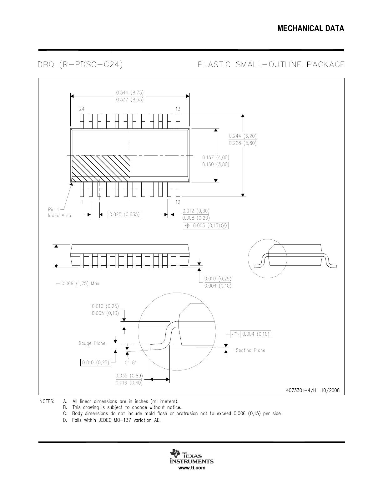
DBQ, DW, OR PWP PACKAGE
(TOP VIEW)
TLC59025
www.ti.com
OUT0– OUT15 Constant-current outputs
...................................................................................................................................................................................................... SLVS934 – JUNE 2009
TERMINAL
NAME
CLK Clock input for data shift on rising edge
GND Ground for control logic and current sink
Data strobe input
LE
OE
R-EXT Input used to connect an external resistor (R
SDI Serial-data input to the Shift register
SDO Serial-data output to the following SDI of next driver IC or to the microcontroller
VDD Supply voltage
Serial data is transferred to the respective latch when LE is high.
The data is latched when LE goes low.
LE has an internal pull-down resistor.
Output enable
When OE is active (low), the output drivers are enabled.
When OE is high, all output drivers are turned OFF (blanked).
OE has an internal pullup resistor.
Terminal Descriptions
DESCRIPTION
) for setting output currents
ext
Copyright © 2009, Texas Instruments Incorporated Submit Documentation Feedback 3
Product Folder Link(s): TLC59025
Page 4

1 2 30 4 6 75 9 10 118 12 14 1513
0
1
off
on
off
on
off
on
off
on
off
on
Don't care
CLK
OE
LE
SDI
OUT0
OUT1
OUT2
OUT3
OUT15
SDO
TLC59025
SLVS934 – JUNE 2009 ......................................................................................................................................................................................................
www.ti.com
Timing Diagram
CLK LE OE SDI OUT0... OUT15... OUT15 SDO
↑ H L Dn Dn...Dn – 7...Dn – 15 Dn – 15
↑ L L Dn + 1 No change Dn – 14
↑ H L Dn + 2 Dn + 2...Dn – 5...Dn – 13 Dn – 13
↓ X L Dn + 3 Dn + 2...Dn – 5...Dn – 13 Dn – 13
↓ X H Dn + 3 off Dn – 13
Figure 1. Timing Diagram
Truth Table in Normal Operation
4 Submit Documentation Feedback Copyright © 2009, Texas Instruments Incorporated
Product Folder Link(s): TLC59025
Page 5
TLC59025
www.ti.com
...................................................................................................................................................................................................... SLVS934 – JUNE 2009
Absolute Maximum Ratings
over operating free-air temperature range (unless otherwise noted)
V
DD
V
I
V
O
I
OUT
I
GND
T
A
T
J
T
stg
Supply voltage 0 7 V
Input voltage – 0.4 V
Output voltage – 0.5 20 V
Output current 45 mA
GND terminal current 750 mA
Operating free-air temperature range – 40 125 ° C
Operating virtual-junction temperature range – 40 150 ° C
Storage temperature range – 55 150 ° C
Power Dissipation and Thermal Impedance
P
D
θ
JA
Power dissipation DW package 2.2 W
Thermal impedance,
junction to free air
Mounted on JEDEC 4-layer board (JESD 51-7),
No airflow, TA= 25 ° C, TJ= 125 ° C
Mounted on JEDEC 1-layer board (JESD 51-3),
No airflow
Mounted on JEDEC 4-layer board (JESD 51-7),
No airflow
MIN MAX UNIT
MIN MAX UNIT
DBQ package 1.6
PW package 1.1
DBQ package 99.8
DW package 80.5
PW package 118.8
DBQ package 61.0
DW package 45.5
PW package 87.9
+ 0.4 V
DD
° C/W
Copyright © 2009, Texas Instruments Incorporated Submit Documentation Feedback 5
Product Folder Link(s): TLC59025
Page 6

TLC59025
SLVS934 – JUNE 2009 ......................................................................................................................................................................................................
Recommended Operating Conditions
over operating free-air temperature range (unless otherwise noted)
V
DD
V
O
I
O
I
OH
I
OL
V
IH
V
IL
t
R
t
F
Supply voltage 3 5.5 V
Output voltage OUT0 to OUT15 17 V
Output current DC test circuit mA
High-level output current SDO – 1 mA
Low-level output current SDO 1 mA
High-level input voltage CLK, OE, LE, and SDI 0.7 × V
Low-level input voltage CLK, OE, LE, and SDI GND 0.3 × V
Rise time CLK 500 ns
Fall time CLK 500 ns
Recommended Timing
V
= 3 V to 5.5 V (unless otherwise noted)
DD
t
w(L)
t
w(CLK)
t
w(OE)
t
su(D)
t
h(D)
t
su(L)
t
h(L)
f
CLK
LE pulse duration 15 ns
CLK pulse duration 15 ns
OE pulse duration 300 ns
Setup time for SDI 3 ns
Hold time for SDI 2 ns
Setup time for LE 5 ns
Hold time for LE 5 ns
Clock frequency Cascade operation 30 MHz
TEST CONDITIONS MIN MAX UNIT
VO≥ 0.6 V 3
VO≥ 1 V 45
DD
V
MIN MAX UNIT
www.ti.com
V
DD
V
DD
6 Submit Documentation Feedback Copyright © 2009, Texas Instruments Incorporated
Product Folder Link(s): TLC59025
Page 7
TLC59025
www.ti.com
...................................................................................................................................................................................................... SLVS934 – JUNE 2009
Electrical Characteristics
V
= 3 V, TJ= – 40 ° C to 125 ° C (unless otherwise noted)
DD
PARAMETER TEST CONDITIONS MIN TYP MAX UNIT
V
DD
V
O
I
O
I
OH
I
OL
V
IH
V
IL
I
leak
V
OH
V
OL
I
O(1)
I
O(2)
I
OUT
V
OUT
T
sd
T
hys
I
DD
C
IN
(1) Specified by design
Input voltage 3 5.5 V
Output voltage 17 V
Output current mA
High-level output current, source -1
Low-level output current, sink 1
High-level input voltage 0.7 × V
Low-level input voltage GND 0.3 × V
Output leakage current V
High-level output voltage SDO, IOL= – 1 mA V
Low-level output voltage SDO, IOH= 1 mA 0.4 V
Output current 1 V
Output current error, die-die ± 3 ± 6 %
Output current error, IOL= 13 mA, VO= 0.6 V, R
channel-to-channel TJ= 25 ° C
Output current 2 VO= 0.8 V, R
Output current error, die-die ± 3 ± 6 %
Output current error, IOL= 26 mA, VO= 0.8 V, R
channel-to-channel TJ= 25 ° C
vs Output current vs
output voltage regulation
Pullup resistance OE 500 k Ω
Pulldown resistance LE 500 k Ω
Overtemperature shutdown
Restart temperature hysteresis 15 ° C
Supply current R
Input capacitance VI= V
VO≥ 0.6 V 3
VO≥ 1 V 45
DD
= 17 V µ A
OH
= 0.6 V, R
OUT
IOL= 13 mA, VO= 0.6 V, R
TJ= 25 ° C
ext
IOL= 26 mA, VO= 0.8 V, R
TJ= 25 ° C
TJ= 25 ° C 0.5
TJ= 125 ° C 2
– 0.4 V
DD
= 1440 Ω 13 mA
ext
= 1440 Ω ,
ext
= 1440 Ω ,
ext
= 720 Ω 26 mA
= 720 Ω ,
ext
= 720 Ω ,
ext
VO= 1 V to 3 V, IO= 13 mA ± 0.1
V
= 3.0 V to 5.5 V, IO= 13 mA to 45 mA ± 1
DD
(1)
R
= Open 7 10
ext
= 1440 Ω 9 12 mA
ext
R
= 720 Ω 11 13
ext
or GND, CLK, SDI, SDO, OE 10 pF
DD
150 175 200 ° C
V
DD
DD
± 1.5 ± 5 %
± 1.5 ± 5 %
mA
V
%/V
Copyright © 2009, Texas Instruments Incorporated Submit Documentation Feedback 7
Product Folder Link(s): TLC59025
Page 8

TLC59025
SLVS934 – JUNE 2009 ......................................................................................................................................................................................................
Electrical Characteristics
V
= 5.5 V, TJ= – 40 ° C to 125 ° C (unless otherwise noted)
DD
PARAMETER TEST CONDITIONS MIN TYP MAX UNIT
V
DD
V
O
I
O
I
OH
I
OL
V
IH
V
IL
I
leak
V
OH
V
OL
I
O(1)
I
O(2)
I
OUT
V
OUT
T
sd
T
hys
I
DD
C
IN
(1) Specified by design
Input voltage 3 5.5 V
Output voltage 17 V
Output current mA
High-level output current, source -1
Low-level output current, sink 1
High-level input voltage 0.7 × V
Low-level input voltage GND 03 × V
Output leakage current V
High-level output voltage SDO, IOL= – 1 mA V
Low-level output voltage SDO, IOH= 1 mA 0.4 V
Output current 1 V
Output current error, die-die ± 3 ± 6 %
Output current error, IOL= 13 mA, VO= 0.6 V, R
channel-to-channel TJ= 25 ° C
Output current 2 VO= 0.8 V, R
Output current error, die-die ± 3 ± 6 %
Output current error, IOL= 26 mA, VO= 0.8 V, R
channel-to-channel TJ= 25 ° C
vs Output current vs
output voltage regulation
Pullup resistance OE 500 k Ω
Pulldown resistance LE 500 k Ω
Overtemperature shutdown
Restart temperature hysteresis 15 ° C
Supply current R
Input capacitance VI= V
VO≥ 0.6 V 3
VO≥ 1 V 45
DD
= 17 V µ A
OH
= 0.6 V, R
OUT
IOL= 13 mA, VO= 0.6 V, R
TJ= 25 ° C
ext
IOL= 26 mA, VO= 0.8 V, R
TJ= 25 ° C
TJ= 25 ° C 0.5
TJ= 125 ° C 2
– 0.4 V
DD
= 1440 Ω 13 mA
ext
= 1440 Ω ,
ext
= 1440 Ω ,
ext
= 720 Ω 26 mA
= 720 Ω ,
ext
= 720 Ω ,
ext
VO= 1 V to 3 V , IO= 26 mA ± 0.1
V
= 3.0 V to 5.5 V, IO= 13 mA to 45 mA ± 1
DD
(1)
R
= Open 9 11
ext
= 1440 Ω 12 14 mA
ext
R
= 720 Ω 14 16
ext
or GND, CLK, SDI, SDO, OE 10 pF
DD
150 175 200 ° C
www.ti.com
V
DD
DD
± 1.5 ± 5 %
± 1.5 ± 5 %
mA
V
%/V
8 Submit Documentation Feedback Copyright © 2009, Texas Instruments Incorporated
Product Folder Link(s): TLC59025
Page 9
TLC59025
www.ti.com
...................................................................................................................................................................................................... SLVS934 – JUNE 2009
Switching Characteristics
V
= 3 V, TJ= – 40 ° C to 125 ° C (unless otherwise noted)
DD
PARAMETER TEST CONDITIONS MIN TYP MAX UNIT
t
PLH1
t
PLH2
t
PLH3
t
PLH4
t
PHL1
t
PHL2
t
PHL3
t
PHL4
t
w(CLK)
t
w(L)
t
w(OE)
t
h(D)
t
su(D)
t
h(L)
t
su(L)
t
r
t
f
t
or
t
of
f
CLK
(1) If the devices are connected in cascade and tror tfis large, it may be critical to achieve the timing required for data transfer between two
cascaded devices.
Low-to-high propagation delay time, CLK to OUTn 30 45 60 ns
Low-to-high propagation delay time, LE to OUTn 30 45 60 ns
Low-to-high propagation delay time, OE to OUTn 30 45 60 ns
Low-to-high propagation delay time, CLK to SDO 30 40 ns
High-to-low propagation delay time, CLK to OUTn 40 65 100 ns
High-to-low propagation delay time, LE to OUTn 40 65 100 ns
High-to-low propagation delay time, OE to OUTn 40 65 100 ns
High-to-low propagation delay time, CLK to SDO 30 40 ns
Pulse duration, CLK 15 ns
Pulse duration LE R
Pulse duration, OE 300 ns
VIH= VDD, VIL= GND,
= 720 Ω , VL= 4 V, 15 ns
ext
RL= 88 Ω , CL= 10 pF
Hold time, SDI 2 ns
Setup time, SDI 3 ns
Hold time, LE 5 ns
Setup time, LE 5 ns
Rise time, CLK
Fall time, CLK
(1)
(1)
500 ns
500 ns
Rise time, outputs (off) 35 50 70 ns
Rise time, outputs (on) 15 50 120 ns
Clock frequency Cascade operation 30 MHz
Copyright © 2009, Texas Instruments Incorporated Submit Documentation Feedback 9
Product Folder Link(s): TLC59025
Page 10

TLC59025
SLVS934 – JUNE 2009 ......................................................................................................................................................................................................
www.ti.com
Switching Characteristics
V
= 5.5 V, TJ= – 40 ° C to 125 ° C (unless otherwise noted)
DD
PARAMETER TEST CONDITIONS MIN TYP MAX UNIT
t
PLH1
t
PLH2
t
PLH3
t
PLH4
t
PHL1
t
PHL2
t
PHL3
t
PHL4
t
w(CLK)
t
w(L)
t
w(OE)
t
h(D)
t
su(D)
t
h(L)
t
su(L)
t
r
t
f
t
or
t
of
f
CLK
(1) If the devices are connected in cascade and tror tfis large, it may be critical to achieve the timing required for data transfer between two
cascaded devices.
Low-to-high propagation delay time, CLK to OUTn 20 35 55 ns
Low-to-high propagation delay time, LE to OUTn 20 35 55 ns
Low-to-high propagation delay time, OE to OUTn 20 35 55 ns
Low-to-high propagation delay time, CLK to SDO 20 30 ns
High-to-low propagation delay time, CLK to OUTn 15 28 42 ns
High-to-low propagation delay time, LE to OUTn 15 28 42 ns
High-to-low propagation delay time, OE to OUTn 15 28 42 ns
High-to-low propagation delay time, CLK to SDO 20 30 ns
Pulse duration, CLK 10 ns
Pulse duration LE R
Pulse duration, OE 200 ns
VIH= VDD, VIL= GND,
= 720 Ω , VL= 4 V, 10 ns
ext
RL= 88 Ω , CL= 10 pF
Hold time, SDI 2 ns
Setup time, SDI 3 ns
Hold time, LE 5 ns
Setup time, LE 5 ns
Rise time, CLK
Fall time, CLK
(1)
(1)
500 ns
500 ns
Rise time, outputs (off) 25 45 65 ns
Rise time, outputs (on) 7 12 20 ns
Clock frequency Cascade operation 30 MHz
10 Submit Documentation Feedback Copyright © 2009, Texas Instruments Incorporated
Product Folder Link(s): TLC59025
Page 11

I
DD
I , I
IH IL
V , V
IH IL
I
ref
I
OUT
V
DD
OE
CLK
LE
SDI
R-EXT
GND
SDO
OUT15
OUT0
V , V
IH IL
Logic input
waveform
V = V
IH DD
V = 0V
IL
I
OUT
R
L
C
L
I
ref
V
DD
OE
CLK
LE
SDI
R-EXT
GND
SDO
OUT15
OUT0
I
DD
Function
Generator
V
L
C
L
TLC59025
www.ti.com
...................................................................................................................................................................................................... SLVS934 – JUNE 2009
PARAMETER MEASUREMENT INFORMATION
Figure 2. Test Circuit for Electrical Characteristics
Figure 3. Test Circuit for Switching Characteristics
Copyright © 2009, Texas Instruments Incorporated Submit Documentation Feedback 11
Product Folder Link(s): TLC59025
Page 12

50%
50%
LOW
Out fput of
Outp t onu
t , t
PLH1 PHL1
t , t
LH2 H 2P LP
CLK
SDI
SDO
LE
OE
OUTn
t , t
PLH4 PHL4
t
w(CLK)
50%
50%
50%
50%
50%
50%
t
su(L)
t
h(L)
t
w(L)
t
su(D)
t
h(D)
50%
t
w(OE)
t
PHL3
t
of
t
or
Output off
t
PLH3
50%
10%
90%
OE
OUTn
50%
90%
50%
10%
HIGH
OE Low
OE Pulsed
TLC59025
SLVS934 – JUNE 2009 ......................................................................................................................................................................................................
www.ti.com
PARAMETER MEASUREMENT INFORMATION (continued)
Figure 4. Normal Mode Timing Waveforms
12 Submit Documentation Feedback Copyright © 2009, Texas Instruments Incorporated
Product Folder Link(s): TLC59025
Page 13

0
10
20
30
40
0 500 1000 1500 2000 2500 3000 3500 4000
R
ext
– P
I
OUT
– mA
W
TLC59025
www.ti.com
...................................................................................................................................................................................................... SLVS934 – JUNE 2009
APPLICATION INFORMATION
Operating Principles
Constant Current
In LED display applications, TLC59025 provides nearly no current variations from channel to channel and from
IC to IC. While I
less than ± 6%.
Adjusting Output Current
TLC59025 sets I
target output current I
I
OUT,target
= (1.21 V / R
Therefore, the default current is approximately 26 mA at 720 Ω and 13 mA at 1440 Ω . The default relationship
after power on between I
≤ 45 mA, the maximum current skew between channels is less than ± 5% and between ICs is
OUT
based on the external resistor R
OUT
OUT,target
ext
in the saturation region:
) × 15.5, where R
OUT,target
and R
ext
is the external resistance connected between R-EXT and GND.
ext
is shown in Figure 5 .
. Users can follow the below formulas to calculate the
ext
Figure 5. Default Relationship Curve Between I
OUT,target
and R
After Power Up
ext
Copyright © 2009, Texas Instruments Incorporated Submit Documentation Feedback 13
Product Folder Link(s): TLC59025
Page 14

TLC59025
SLVS934 – JUNE 2009 ......................................................................................................................................................................................................
Propagation Delay Times
www.ti.com
Figure 6. CLK to OUT7
Figure 7. OE to OUT1
14 Submit Documentation Feedback Copyright © 2009, Texas Instruments Incorporated
Product Folder Link(s): TLC59025
Page 15

TLC59025
www.ti.com
...................................................................................................................................................................................................... SLVS934 – JUNE 2009
Figure 8. OE to OUT7
Copyright © 2009, Texas Instruments Incorporated Submit Documentation Feedback 15
Product Folder Link(s): TLC59025
Page 16

PACKAGE OPTION ADDENDUM
www.ti.com 2-Jul-2009
PACKAGING INFORMATION
Orderable Device Status
(1)
Package
TLC59025IDBQR ACTIVE SSOP/
(1)
The marketingstatus values are defined as follows:
Type
QSOP
Package
Drawing
Pins Package
Qty
Eco Plan
DBQ 24 2500 Green (RoHS &
no Sb/Br)
(2)
Lead/Ball Finish MSL Peak Temp
CU NIPDAU Level-2-260C-1 YEAR
(3)
ACTIVE: Productdevice recommended for new designs.
LIFEBUY: TIhas announced that the device will be discontinued, and a lifetime-buyperiod is in effect.
NRND: Not recommended for new designs. Device is in production to support existing customers, but TI does not recommend using this part in
a newdesign.
PREVIEW: Devicehas been announced but is not in production. Samples may ormay not be available.
OBSOLETE: TIhas discontinued the production of the device.
(2)
Eco Plan - The planned eco-friendly classification: Pb-Free (RoHS), Pb-Free (RoHS Exempt), or Green (RoHS & no Sb/Br) - please check
http://www.ti.com/productcontent forthe latest availability information and additional product content details.
TBD: ThePb-Free/Green conversion plan has not been defined.
Pb-Free (RoHS): TI's terms "Lead-Free" or "Pb-Free" mean semiconductor products that are compatible with the current RoHS requirements
for all 6 substances, including the requirement that lead not exceed 0.1% by weight in homogeneous materials. Where designed to be soldered
at hightemperatures, TI Pb-Free products are suitable for use in specified lead-freeprocesses.
Pb-Free (RoHS Exempt): This component has a RoHS exemption for either 1) lead-based flip-chip solder bumps used between the die and
package, or 2) lead-based die adhesive used between the die and leadframe. The component is otherwise considered Pb-Free (RoHS
compatible) asdefined above.
Green (RoHS & no Sb/Br): TI defines "Green" to mean Pb-Free (RoHS compatible), and free of Bromine (Br) and Antimony (Sb) based flame
retardants (Bror Sb do not exceed 0.1% by weight in homogeneous material)
(3)
MSL, Peak Temp. -- The Moisture Sensitivity Level rating according to the JEDEC industry standard classifications, and peak solder
temperature.
Important Information and Disclaimer:The information provided on this page represents TI's knowledge and belief as of the date that it is
provided. TI bases its knowledge and belief on information provided by third parties, and makes no representation or warranty as to the
accuracy of such information. Efforts are underway to better integrate information from third parties. TI has taken and continues to take
reasonable steps to provide representative and accurate information but may not have conducted destructive testing or chemical analysis on
incoming materials and chemicals. TI and TI suppliers consider certain information to be proprietary, and thus CAS numbers and other limited
information maynot be available for release.
In no event shall TI's liability arising out of such information exceed the total purchase price of the TI part(s) at issue in this document sold by TI
to Customeron an annual basis.
Addendum-Page 1
Page 17
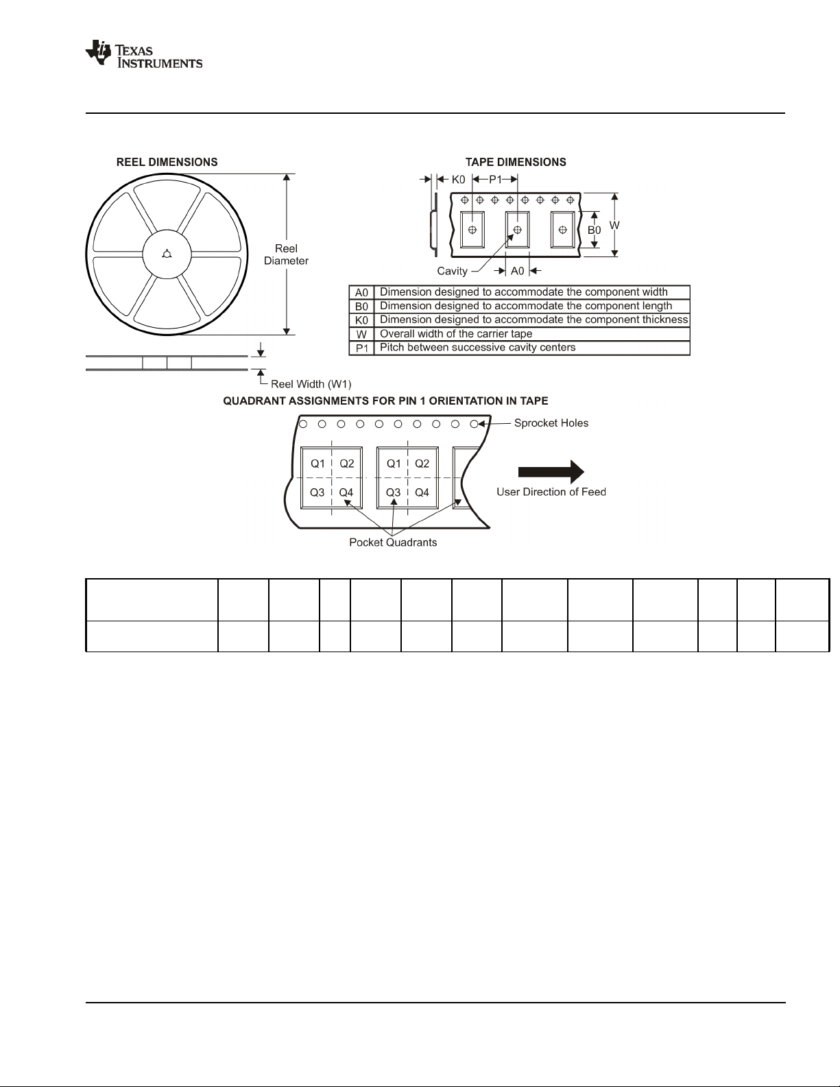
PACKAGE MATERIALS INFORMATION
www.ti.com 30-Jun-2009
TAPE AND REEL INFORMATION
*All dimensions are nominal
Device Package
TLC59025IDBQR SSOP/
Type
QSOP
Package
Drawing
Pins SPQ Reel
Diameter
(mm)
DBQ 24 2500 330.0 16.4 6.5 9.0 2.1 8.0 16.0 Q1
Reel
Width
W1 (mm)
A0 (mm) B0 (mm) K0 (mm) P1
(mm)W(mm)
Pin1
Quadrant
Pack Materials-Page1
Page 18
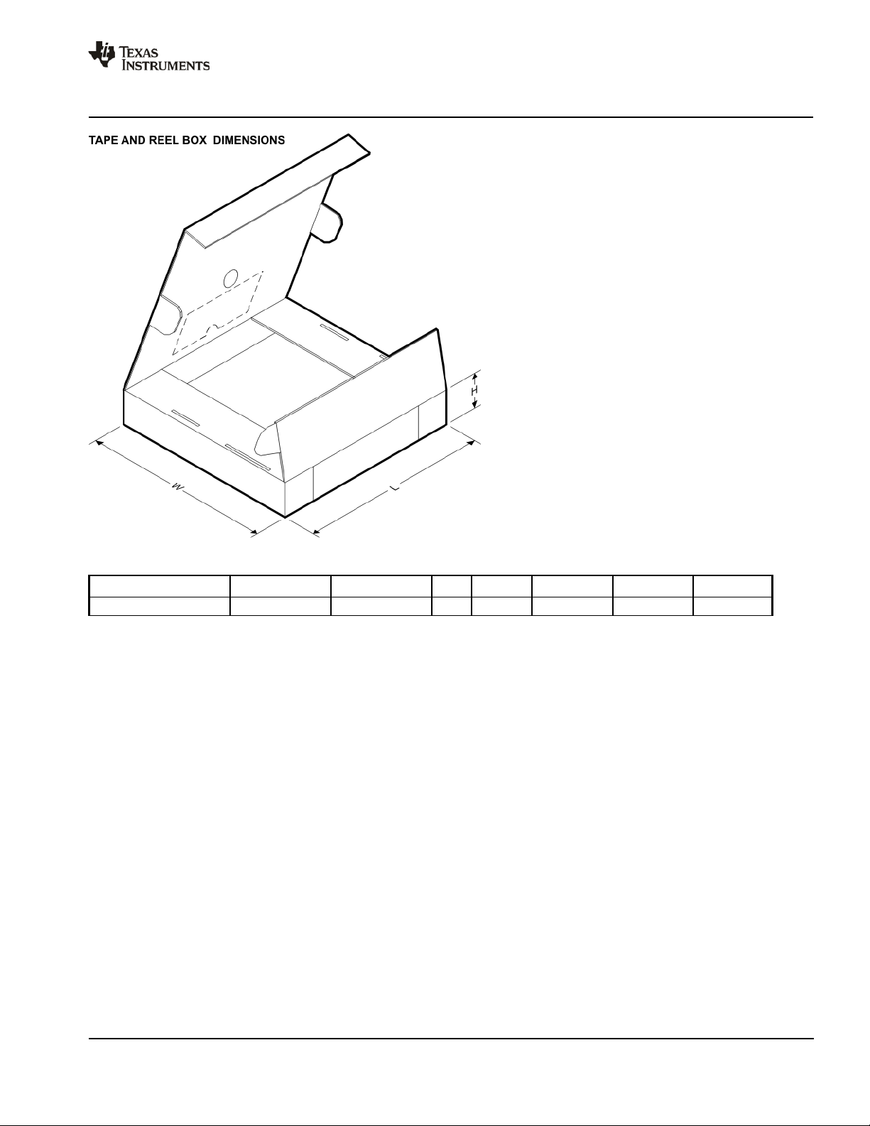
PACKAGE MATERIALS INFORMATION
www.ti.com 30-Jun-2009
*All dimensions are nominal
Device Package Type Package Drawing Pins SPQ Length (mm) Width (mm) Height (mm)
TLC59025IDBQR SSOP/QSOP DBQ 24 2500 346.0 346.0 33.0
Pack Materials-Page2
Page 19
Page 20
Page 21

IMPORTANT NOTICE
Texas Instruments Incorporated and its subsidiaries (TI) reserve the right to make corrections, modifications, enhancements, improvements,
and other changes to its products and services at any time and to discontinue any product or service without notice. Customers should
obtain the latest relevant information before placing orders and should verify that such information is current and complete. All products are
sold subject to TI’s terms and conditions of sale supplied at the time of order acknowledgment.
TI warrants performance of its hardware products to the specifications applicable at the time of sale in accordance with TI’s standard
warranty. Testing and other quality control techniques are used to the extent TI deems necessary to support this warranty. Except where
mandated by government requirements, testing of all parameters of each product is not necessarily performed.
TI assumes no liability for applications assistance or customer product design. Customers are responsible for their products and
applications using TI components. To minimize the risks associated with customer products and applications, customers should provide
adequate design and operating safeguards.
TI does not warrant or represent that any license, either express or implied, is granted under any TI patent right, copyright, mask work right,
or other TI intellectual property right relating to any combination, machine, or process in which TI products or services are used. Information
published by TI regarding third-party products or services does not constitute a license from TI to use such products or services or a
warranty or endorsement thereof. Use of such information may require a license from a third party under the patents or other intellectual
property of the third party, or a license from TI under the patents or other intellectual property of TI.
Reproduction of TI information in TI data books or data sheets is permissible only if reproduction is without alteration and is accompanied
by all associated warranties, conditions, limitations, and notices. Reproduction of this information with alteration is an unfair and deceptive
business practice. TI is not responsible or liable for such altered documentation. Information of third parties may be subject to additional
restrictions.
Resale of TI products or services with statements different from or beyond the parameters stated by TI for that product or service voids all
express and any implied warranties for the associated TI product or service and is an unfair and deceptive business practice. TI is not
responsible or liable for any such statements.
TI products are not authorized for use in safety-critical applications (such as life support) where a failure of the TI product would reasonably
be expected to cause severe personal injury or death, unless officers of the parties have executed an agreement specifically governing
such use. Buyers represent that they have all necessary expertise in the safety and regulatory ramifications of their applications, and
acknowledge and agree that they are solely responsible for all legal, regulatory and safety-related requirements concerning their products
and any use of TI products in such safety-critical applications, notwithstanding any applications-related information or support that may be
provided by TI. Further, Buyers must fully indemnify TI and its representatives against any damages arising out of the use of TI products in
such safety-critical applications.
TI products are neither designed nor intended for use in military/aerospace applications or environments unless the TI products are
specifically designated by TI as military-grade or "enhanced plastic." Only products designated by TI as military-grade meet military
specifications. Buyers acknowledge and agree that any such use of TI products which TI has not designated as military-grade is solely at
the Buyer's risk, and that they are solely responsible for compliance with all legal and regulatory requirements in connection with such use.
TI products are neither designed nor intended for use in automotive applications or environments unless the specific TI products are
designated by TI as compliant with ISO/TS 16949 requirements. Buyers acknowledge and agree that, if they use any non-designated
products in automotive applications, TI will not be responsible for any failure to meet such requirements.
Following are URLs where you can obtain information on other Texas Instruments products and application solutions:
Products Applications
Amplifiers amplifier.ti.com Audio www.ti.com/audio
Data Converters dataconverter.ti.com Automotive www.ti.com/automotive
DLP® Products www.dlp.com Broadband www.ti.com/broadband
DSP dsp.ti.com Digital Control www.ti.com/digitalcontrol
Clocks and Timers www.ti.com/clocks Medical www.ti.com/medical
Interface interface.ti.com Military www.ti.com/military
Logic logic.ti.com Optical Networking www.ti.com/opticalnetwork
Power Mgmt power.ti.com Security www.ti.com/security
Microcontrollers microcontroller.ti.com Telephony www.ti.com/telephony
RFID www.ti-rfid.com Video & Imaging www.ti.com/video
RF/IF and ZigBee® Solutions www.ti.com/lprf Wireless www.ti.com/wireless
Mailing Address: Texas Instruments, Post Office Box 655303, Dallas, Texas 75265
Copyright © 2009, Texas Instruments Incorporated
 Loading...