

T
20 MSPS 3-CHANNEL ANALOG-TO-DIGITAL CONVERTER
WITH HIGH-PRECISION CLAMP
SLAS104A – JULY 1995 – REVISED NOVEMBER 1996
D
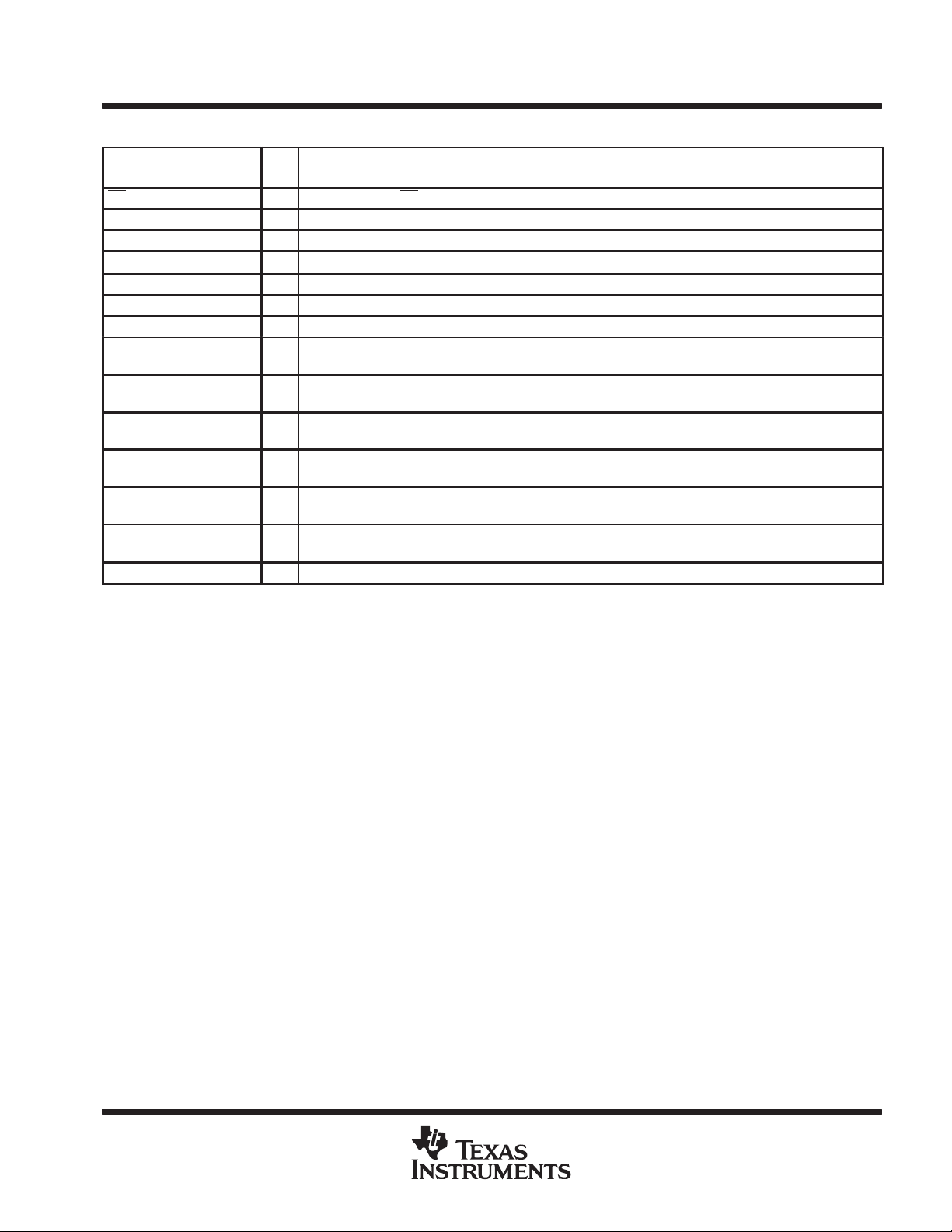
3-Channel CMOS ADC
D
5-V Single-Supply Operation or 5-V Analog
Supply with Digital Supply from
2.7 V to 5.25 V
D
8-Bit Resolution
D
Differential Linearity Error...±0.5 LSB Max
D
Linearity Error...±0.75 LSB Max
D
Maximum Conversion Rate
20 Megasamples per Second
(MSPS) Min
D
Analog Input Voltage Range
2 V
D
64-Pin Shrink QFP Package
I(PP)
Min
description
The TLC5733A is a 3-channel 8-bit semiflash analog-to-digital converter (ADC) that operates from a single 5-V
power supply. It converts a wide-band analog signal (such as a video signal) to digital data at sampling rates
up to 20 MSPS minimum. The TLC5733A contains a feed-back type high-precision clamp circuit for each ADC
channel for video (YUV) applications and a clamp pulse generator that detects COMPOSITE SYNC
automatically . A clamp pulse can also be supplied externally . The output-data format multiplexer selects a ratio
of Y:U:V of 4:4:4, 4:1:1, or 4:2:2. For RGB applications, the 4:4:4 output format without clamp function can be
used. The TLC5733A is characterized for operation from –20°C to 75°C.
D
Analog Input Bandwidth...>14 MHz
D
Suitable for YUV or RGB Applications
D
Digital Clamp Optimized for NTSC or PAL
YUV Component
D
High-Precision Clamp...±1 LSB
D
Automatic Clamp Pulse Generator
D
Output-Data Format Multiplexer
D
Low Power Consumption
TLC5733A
†
pulses
AVAILABLE OPTIONS
A
–20°C to 75°C TLC5733AIPM
Please be aware that an important notice concerning availability, standard warranty, and use in critical applications of
Texas Instruments semiconductor products and disclaimers thereto appears at the end of this data sheet.
†
COMPOSITE SYNC refers to the externally generated synchronizing signal that is a combination of vertical and horizontal sync information
used in display and TV systems.
PACKAGE
QUAD FLATPACK
PRODUCTION DATA information is current as of publication date.
Products conform to specifications per the terms of Texas Instruments
standard warranty. Production processing does not necessarily include
testing of all parameters.
POST OFFICE BOX 655303 • DALLAS, TEXAS 75265
Copyright 1996, Texas Instruments Incorporated
1
TLC5733A
20 MSPS 3-CHANNEL ANALOG-TO-DIGITAL CONVERTER
WITH HIGH-PRECISION CLAMP
SLAS104A – JULY 1995 – REVISED NOVEMBER 1996
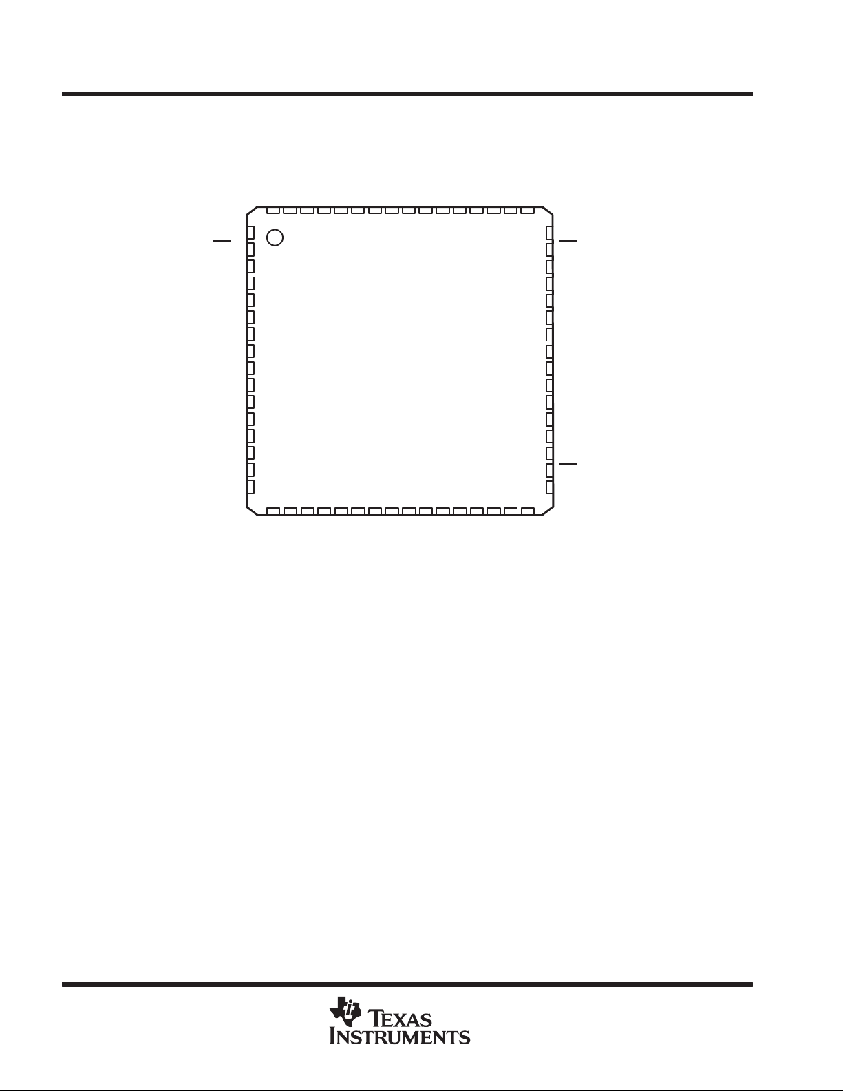
PM PACKAGE
(TOP VIEW)
RB A
A
OE
NT/PAL
TEST
QA DGND
AD8
AD7
AD6
AD5
AD4
AD3
AD2
AD1
QA DV
DD
DGND
QB DV
DD
CC
AV
A
GND A
AIN
63 62 61 60 5964 58
1
2
3
4
5
6
7
8
9
10
11
12
13
14
15
16
18 19
17
BD6
BD8
BD7
RT A
CLPV A
21 22 23 24
20
BD5
BD4
CLP OUT A
BD3
INIT
CLPEN
CLK
56 55 5457
25 26 27 28 29
BD2
BD1
QB DGND
CLP OUT B
EXTCLP
53 52
DD
DV
CLP OUT C
CLPV B
RT B
51 50 49
30 31 32
RT C
CLPV C
C A V
CC
AVB
CC
BIN
CIN
GND B
RB B
48
OE
47
MODE0
46
MODE1
45
QC DGND
44
CD1
43
CD2
42
CD3
41
CD4
40
CD5
39
38
CD6
37
CD7
36
CD8
35
QC DV
34
OE C
33
RB C
GND C
B
DD
2
POST OFFICE BOX 655303 • DALLAS, TEXAS 75265
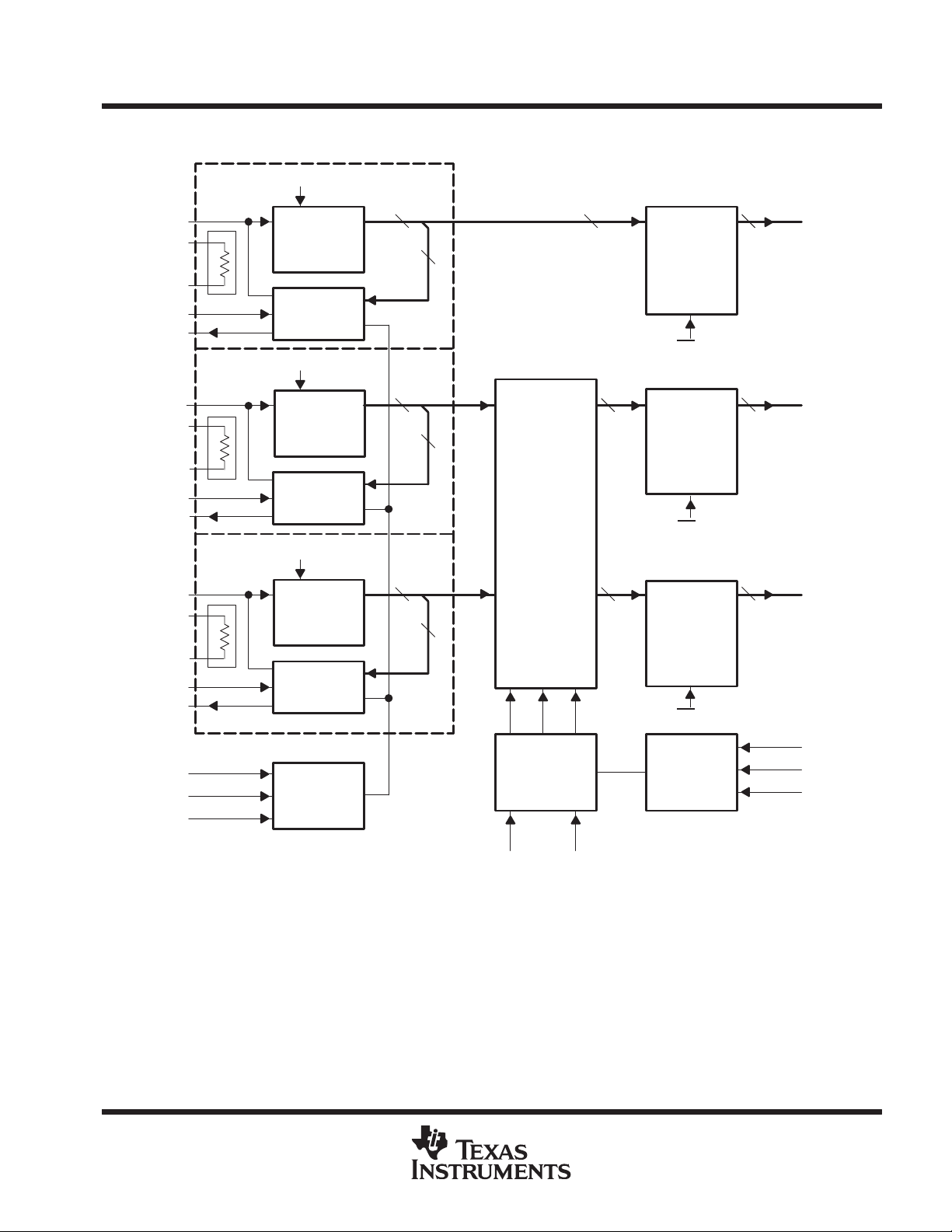
functional block diagram
CLK A
TLC5733A
20 MSPS 3-CHANNEL ANALOG-TO-DIGITAL CONVERTER
WITH HIGH-PRECISION CLAMP
SLAS104A – JULY 1995 – REVISED NOVEMBER 1996
AIN
RT A
RB A
CLPV A
CLP OUT A
BIN
RT B
RB B
CLPV B
CLP OUT B
CIN
RT C
RB C
CLPV C
CLP OUT C
ADC
(Sampling
Comparators)
Clamp
Circuit
CLK B
ADC
(Sampling
Comparators)
Clamp
Circuit
CLK C
ADC
(Sampling
Comparators)
Clamp
Circuit
8
8
8
8
Multiplexer
For
Output Format
8
8
8
Output Data
Latch
OE A
8
Output Data
Latch
OE B
8
Output Data
Latch
OE C
8
8
8
AD1–8
BD1–8
CD1–8
EXTCLP
CLPEN
NT/PAL
Control For
INT/EXT
Clamp Circuit
Clock
Generator
CLK INIT
POST OFFICE BOX 655303 • DALLAS, TEXAS 75265
Output
Format
Selector
and Test
MODE0
MODE1
TEST
3
TLC5733A
I/O
DESCRIPTION
20 MSPS 3-CHANNEL ANALOG-TO-DIGITAL CONVERTER
WITH HIGH-PRECISION CLAMP
SLAS104A – JULY 1995 – REVISED NOVEMBER 1996
Terminal Functions
TERMINAL
NAME NO.
A AV
CC
AD8–AD1 6–13 O Data output of ADC A (LSB: AD1, MSB:AD8)
AIN 63 I Analog input of ADC A
B AV
CC
BD8–BD1 17–24 O Data output of ADC B (LSB: BD1, MSB:BD8)
BIN 50 I Analog input of ADC B
C AV
CC
CD8–CD1 36–43 O Data output of ADC C (LSB:CD1, MSB: CD8)
CIN 31 I Analog input of ADC C
CLK 56 I Clock input. The clock frequency is normally 4 × the frequency subcarrier (fsc) for most video systems (see
CLPEN 57 I Clamp enable. When using an internal clamp pulse, CLPEN should be high. When using an external clamp
CLP OUT A 59 O Clamping bias current of ADC A. A resistor-capacitor combination that sets the clamp timing.
CLP OUT B 54 O Clamping bias current of ADC B. A resistor-capacitor combination that sets the clamp timing.
CLP OUT C 27 O Clamping bias current of ADC C. A resistor-capacitor combination that sets the clamp timing.
CLPV A 60 O Clamping level of ADC A. A capacitor is connected to CLPV A to set the clamp timing. The clamp level at
CLPV B 53 O Clamping level of ADC B. A capacitor is connected to CLPV B to set the clamp timing. The clamp level at
CLPV C 28 O Clamping level of ADC C. A capacitor is connected to CLPV C to set the clamp timing. The clamp level at
DGND 15 I Digital ground
DV
DD
EXTCLP 55 I External clamp pulse input. When EXTCLP and CLPEN are low, the internal clamp circuit cannot be used.
GND A 64 I Ground of ADC A
GND B 49 I Ground of ADC B
GND C 32 I Ground of ADC C
INIT 58 I Output initialized. The output data is synchronous when INIT is taken high from low. INIT is a control terminal
MODE0 46 I Output format mode selector 0. When MODE1 is low and MODE0 is low, output data format1 is selected.
MODE1 45 I Output format mode selector 1. When MODE1 is low and MODE0 is low, output data format1 is selected.
NT/PAL 3 I NTSC/PAL control. NTSC/PAL should be low for NTSC and high for PAL.
OE A 2 I Output enable A. OE A enables the output of ADC A.
OE B 47 I Output enable B. OE B enables the output of ADC B.
62 I Analog supply voltage of ADC A
51 I Analog supply voltage of ADC B
30 I Analog supply voltage of ADC C
When MODE0 = L, MODE1 = L, CD8 outputs MSB flag of BD8–BD5
When MODE0 = L, MODE1 = L, CD7 outputs MSB flag of BD8–BD5
When MODE0 = L, MODE1 = H, CD8 outputs B channel flag of CD8–BD1
When MODE0 = L, MODE1 = H, CD8 outputs B channel flag of CD8–BD1
T able 3). The nominal clock frequency is 14.31818 MHz for National T elevision System Committee (NTSC)
and 17.745 MHz for phase alteration line (PAL).
pulse, CLPEN should be low.
CLPV A is connected to an output code of 16 (0010000).
CLPV B is connected to an output code of 128 (1000000).
CLPV C is connected to an output code of 128 (1000000).
26 I Digital supply voltage
The external clamp pulse when used is active high.
that allows the external system to initialize the TLC5733A data conversion cycle. INIT is usually used at
power up or system reset.
When MODE1 is low and MODE0 is high, output data format2 is selected. When MODE1 is high and
MODE0 is low, output data format3 is selected. A high level on MODE1 and a high level on MODE0 is not
used.
When MODE1 is low and MODE0 is high, output data format2 is selected. When MODE1 is high and
MODE0 is low, output data format3 is selected. A high level on MODE1 and a high level on MODE0 is not
used.
4
POST OFFICE BOX 655303 • DALLAS, TEXAS 75265
I/O
DESCRIPTION
TLC5733A
20 MSPS 3-CHANNEL ANALOG-TO-DIGITAL CONVERTER
WITH HIGH-PRECISION CLAMP
SLAS104A – JULY 1995 – REVISED NOVEMBER 1996
Terminal Functions (Continued)
TERMINAL
NAME NO.
OE C 34 I Output enable C. OE C enables the output of ADC C.
QA DGND 5 I Digital ground for output of ADC A
QA DV
DD
QB DGND 25 I Digital ground for output of ADC B
QB DV
DD
QC DGND 44 I Digital ground for output of ADC C
QC DV
DD
RB A 1 I Bottom reference voltage of ADC A. The nominal externally applied dc voltage between RT A and RB A is
RB B 48 I Bottom reference voltage of ADC B. The nominal externally applied dc voltage between RT B and RB B is
RB C 33 I Bottom reference voltage of ADC C. The nominal externally applied dc voltage between RT C and RB C
RT A 61 I Top reference voltage of ADC A. The nominal externally applied dc voltage between RT A and RB A is 2
RT B 52 I Top reference voltage of ADC B. The nominal externally applied dc voltage between RT B and RB B is 2
RT C 29 Top reference voltage of ADC C. The nominal externally applied dc voltage between RT C and RB C is 2
TEST 4 I Test. TEST should be tied low when using this device.
14 I Digital supply voltage for output of ADC A
16 I Digital supply voltage for output of ADC B
35 I Digital supply voltage for output of ADC C
2 V for video signals.
2 V for video signals.
is 2 V for video signals.
V for video signals.
V for video signals.
V for video signals.
absolute maximum ratings
Supply voltage, V
Reference voltage input range,V
V
ref(RB B)
Analog input voltage range AGND to V
Digital input voltage range, V
Digital output voltage range, V
Operating free-air temperature range, T
Storage temperature range, T
†
Stresses beyond those listed under “absolute maximum ratings” may cause permanent damage to the device. These are stress ratings only, and
functional operation of the device at these or any other conditions beyond those indicated under “recommended operating conditions” is not
implied. Exposure to absolute-maximum-rated conditions for extended periods may affect device reliability.
, V
ref(RB C)
CC
†
, VDD 7 V. . . . . . . . . . . . . . . . . . . . . . . . . . . . . . . . . . . . . . . . . . . . . . . . . . . . . . . . . . . . . . . . . . .
AGND to V
ref(RT A)
. . . . . . . . . . . . . . . . . . . . . . . . . . . . . . . . . . . . . . . . . . . . . . . . . . . . . . . . . . .
, V
ref(RT B)
, V
ref(RT C)
, V
ref(RB A)
,
. . . . . . . . . . . . . . . . . . . . . . . . . . . . . . . . . . . . . . . . . . . . . . . . . . . . . . . . .
DGND to V
. . . . . . . . . . . . . . . . . . . . . . . . . . . . . . . . . . . . . . . . . . . . . . . . . . . . . . .
I
DGND to V
. . . . . . . . . . . . . . . . . . . . . . . . . . . . . . . . . . . . . . . . . . . . . . . . . . . .
O
–55°C to 150°C. . . . . . . . . . . . . . . . . . . . . . . . . . . . . . . . . . . . . . . . . . . . . . . . . . .
stg
–20°C to 75°C. . . . . . . . . . . . . . . . . . . . . . . . . . . . . . . . . . . . . . . . . . . .
A
CC
CC
DD
DD
POST OFFICE BOX 655303 • DALLAS, TEXAS 75265
5
TLC5733A
‡
V
A
V
A
20 MSPS 3-CHANNEL ANALOG-TO-DIGITAL CONVERTER
WITH HIGH-PRECISION CLAMP
SLAS104A – JULY 1995 – REVISED NOVEMBER 1996
recommended operating conditions
MIN NOM MAX UNIT
VCC–AGND 4.75 5 5.25
Supply voltage
Reference input voltage, V
Reference input voltage, V
Analog input voltage, V
High-level input voltage, V
Low-level input voltage, V
High-level pulse duration, t
Low-level pulse duration, t
Setup time for INIT input, t
Operating free-air temperature range, T
‡
Within the electrical and operating characteristics table, when the term VDD is used, all XDVDD terminals are tied together, and when the term
VCC is used, all XAVCC terminals are tied together.
VDD–DGND 2.7 5 5.25
AGND–DGND –100 0 100 mV
ref(RT A)
ref(RB A)
I
IH
IL
w(H)
w(L)
su1
, V
ref(RT B)
, V
ref(RB B)
, V
ref(RT C)
, V
ref(RB C)
A
V
+2 V
ref(RB)
0 V
0 V
2 V
25 ns
25 ns
5 ns
–20 75 °C
CC
ref(RT)
ref(RT)
0.8 V
–2 V
V
V
electrical characteristics at VDD = 2.7 V to 5.25 V, V
f
†
= 20 MHz, TA = 25°C (unless otherwise noted)
(CLK)
PARAMETER TEST CONDITIONS MIN TYP MAX UNIT
Clamp level accuracy ±1 LSB
R
ref
C
i
I
IH
I
IL
V
OH
V
OL
I
OH(lkg)
I
OL(lkg)
I
CC
Conditions marked MIN or MAX are as stated in recommended operating conditions.
Reference voltage resistor Measured between RT and RB 160 220 350 Ω
Analog input capacitance VI = 1.5 V + 0.07 V
High-level input current
Low-level input current
High-level output voltage
Low-level output voltage
High-level output leakage current
Low-level output leakage current
Supply current
VDD = MAX†,
VCC = 5V
VDD = MAX†,
VCC = 5V
All DVDD terminals = 2.7 V to 5.25 V,
IOH = –1 mA
All DVDD terminals = 2.7 V to 5.25 V,
IOL = 2 mA
VDD = MAX†,
VCC = 5V
VDD = MIN†,
VCC = 5V
fc = 20 MSPS,
NTSC ramp wave input
CC
rms
= 5 V, V
ref(RT)
VIH = VDD,
VIL = 0,
VOH = VDD,
VOL = 0,
= 2.5 V, V
DVDD –0.7 V
ref(BB)
= 0.5 V,
16 pF
50 75 mA
5
µ
5
0.8
16
µ
16
6
POST OFFICE BOX 655303 • DALLAS, TEXAS 75265
TLC5733A
20 MSPS 3-CHANNEL ANALOG-TO-DIGITAL CONVERTER
WITH HIGH-PRECISION CLAMP
SLAS104A – JULY 1995 – REVISED NOVEMBER 1996
operating characteristics at VDD = 2.7 V to 5.25 V, V
f
‡
= 20 MHz, TA = 25°C (unless otherwise noted)
(CLK)
PARAMETER TEST CONDITIONS MIN TYP MAX UNIT
E
Zero-scale error V
ZS
E
Full-scale error V
FS
E
Linearity error
L
E
Linearity error, differential
D
f
Maximum conversion rate VI = 0.5 V – 2.5 V, fI = 1-kHz ramp waveform 20 MSPS
c
BW Analog input bandwidth At – 1 dB 14 MHz
t
Digital output delay time CL = 10 pF 18 30 ns
pd
Differential gain NTSC 40 IRE‡ modulation wave, fc = 14.3 MSPS 1%
Differential phase NTSC 40 IRE‡ modulation wave, fc = 14.3 MSPS 0.7 deg
Aperture jitter time 30 ps
Sampling delay time 4 ns
Institute of Radio Engineers
= REFT – REFB = 2 V –18 –43 –68 mV
ref
= REFT – REFB = 2 V –20 0 20 mV
ref
f
= 20 MHz, VI = 0.5 V to 2.5 V ±0.4 ±0.75
(CLK)
f
= 20 MHz,
(CLK)
TA = –20°C to 75°C
f
= 20 MHz, VI = 0.5 V to 2.5 V ±0.3 ±0.5
(CLK)
f
= 20 MHz,
(CLK)
TA = –20°C to 75°C
= 5 V, V
CC
VI = 0.5 V to 2.5 V
VI = 0.5 V to 2.5 V
ref(RT)
= 2.5 V, V
ref(RB)
= 0.5 V,
±0.4 ±1
±0.3 ±0.75
LSB
LSB
POST OFFICE BOX 655303 • DALLAS, TEXAS 75265
7
TLC5733A
CHANNEL OF ADC
OUTPUT CODE
APPLICATION
L
H
COMPOSITE SYNC input
20 MSPS 3-CHANNEL ANALOG-TO-DIGITAL CONVERTER
WITH HIGH-PRECISION CLAMP
SLAS104A – JULY 1995 – REVISED NOVEMBER 1996
detailed description
clamp function
The clamp function is optimized for a YUV video signal and has two clamp modes. The first mode uses the
COMPOSITE SYNC signal as the input to the EXTCLP terminal to generate an internal clamp pulse and the
second mode uses an externally generated clamp pulse as the input to the EXTCLP terminal.
In the first mode, the device detects false pulses in the COMPOSITE SYNC signal by monitoring the rising and
falling edges of the COMPOSITE SYNC signal pulses. This monitoring prevents faulty operation caused by
disturbances and missing pulses of the COMPOSITE SYNC signal input on EXTCLP and external spike noise.
When fault pulses are detected, the device internally generates a train of clamp pulses at the proper positions
(1H) by an internal 910-counter for NTSC and a 1 136-counter for P AL. The device checks clamp pulses for 1H
time and generates clamp pulses at correct positions when COMPOSITE SYNC pulses are in error in time.
The internal counter continually produces a horizontal sync period (1H) that is NTSC or PAL compatible as
selected by the condition of the NT/PAL terminal.
clamp voltages and selection
T able 1 shows the clamping level during the clamp interval. T able 2 shows the selection of the internal or external
clamp pulse. With either NTSC or PAL, the internal clamp pulse is always used.
Table 1. Clamp Level (Internal Connection Level)
ADC A • V
ADC B • V
ADC C • V
I(A)
I(B)
I(C)
00010000 Y
10000000 (U, V)
10000000 (U, V)
Table 2. Clamp Level (Internal Connection Level)
CONDITION FUNCTION (EACH ADC)
CLPEN EXTCLP NT/PAL INTERNAL CLAMP CLAMP PULSE
Don’t Care Inactive External clamp pulse
L Don’t Care Inactive No clamping
p
L Active Synchronous with NTSC
H Active Synchronous with P AL
The clamp circuit is shown in Figure 6. The clamp voltage is stored on capacitor C2 during the back porch of
the horizontal blanking period.
During the clamp pulse the input to channel A is clamped to:
V
(A) = (16/256) × (voltage difference from terminal RT A to RB A)
C
V
(B) = (128/256) × (voltage difference from terminal RT B to RB B)
C
V
(C) = (128/256) × (voltage difference from terminal RT C to RB C)
C
COMPOSITE SYNC time monitoring
When CLPEN is high, COMPOSITE SYNC generates an internal clamp pulse on the horizontal blanking interval
back porch. The TLC5733A has a timing window into which the horizontal sync tip must occur. There is a noise
time window for the falling edge and one for the rising edge (see Figure 1, Figure 2, and Table 3).
8
POST OFFICE BOX 655303 • DALLAS, TEXAS 75265

20 MSPS 3-CHANNEL ANALOG-TO-DIGITAL CONVERTER
WITH HIGH-PRECISION CLAMP
SLAS104A – JULY 1995 – REVISED NOVEMBER 1996
correct COMPOSITE SYNC timing
The Noise Gate 1 signal provides the timing window for the COMPOSITE SYNC falling edge. After an interval
A of 867 clocks for NTSC or 1075 for P AL from the last falling edge of COMPOSITE SYNC, Noise Gate 1 signal
goes high for 43 clocks for NTSC or 61 clocks for PAL (interval B). The falling edge of the input signal to the
EXTCLP terminal can occur at any time within this window to be a valid COMPOSITE SYNC falling edge.
The Noise Gate 2 signal provides the timing window for the COMPOSITE SYNC rising edge. On the falling edge
of the horizontal sync tip, the internal logic generates Noise Gate 2 as a low signal for 58 clocks (interval C) for
both NTSC and P AL and then returns to a high active state. At this time if the input to EXTCLP is still low, it is
considered a valid COMPOSITE SYNC signal.
normal clamp pulse generation
On the rising edge of COMPOSITE SYNC, the internal logic generates an internal delay (interval D) and then
generates the internal positive clamp pulse 54 clocks wide (interval F).
clamp operation with incorrect COMPOSITE SYNC timing
noise suppression
If the input to EXTCLP goes low prior to Noise Gate 1 going high (within 43 clocks for NTSC or 61 clocks for
P AL of the normal 1H timing for the falling edge of COMPOSITE SYNC) then that input is not considered a valid
COMPOSITE SYNC and is ignored.
TLC5733A
If the input to EXTCLP is high when Noise Gate 2 goes to the high state, the input signal is considered noise
and is ignored.
Therefore, the correct signal must be high for a maximum of 43 clocks for NTSC or 61 clocks for P AL, before
the 1H timing, to be a valid sync signal. Also, the input to EXTCLP must be at least 58 clocks wide (interval C)
to be valid.
This function of monitoring the timing eliminates spurious noise spikes from falsely synchronizing the system.
timing error of COMPOSITE SYNC
The internal counter resets to zero on the first falling edge of COMPOSITE SYNC. After that time, if there is a
missing COMPOSITE SYNC signal, then the internal logic waits an interval of 76 clocks (interval E) for NTSC
or 93 for PAL from the counter zero count and then generates an internal clamp pulse 54 clocks wide
(interval F).
This function maintains the synchronization pattern when COMPOSITE SYNC is not present.
summary of device operation with COMPOSITE SYNC
This internal timing allows the TLC5733A to correctly position the clamp pulse when an external COMPOSITE
SYNC input:
• Is delayed with respect to the horizontal sync period
• Is early with respect to the horizontal sync period
• Is nonexistent during the horizontal sync period
• Has falling edge noise spikes within the horizontal sync period
The device operation is summarized as follows for these improper external clamp conditions:
• Under all four conditions on EXTCLP, the internal clamp generation circuit generates a clamp pulse at
the proper time after the horizontal sync period as shown in Figure 1.
• The TLC5733A internal clamp circuit generates an internal clamp pulse each 1H time for the entire time
interval that the COMPOSITE SYNC input is missing.
POST OFFICE BOX 655303 • DALLAS, TEXAS 75265
9

TLC5733A
20 MSPS 3-CHANNEL ANALOG-TO-DIGITAL CONVERTER
WITH HIGH-PRECISION CLAMP
SLAS104A – JULY 1995 – REVISED NOVEMBER 1996
1H
COMPOSITE
SYNC
B A
Noise Gate 1
C
Noise Gate 2
F
Internal Clamp
Pulse
D
Missing COMPOSITE SYNC,
therefore, Noise Gate is Not
Generated
FE
NTSC/PAL Counter Reset NTSC/PAL Counter at
Max Count
Figure 1. COMPOSITE SYNC and Internal Clamp Timing
COMPOSITE
SYNC
B
Noise Gate 1
Noise Gate 2
Figure 2. Proper COMPOSITE SYNC Timing
Table 3. Sync and Clamp Timing for NTSC and PAL with CLK = 4 fsc
NTSC
TIME
INTERVAL
A 867 60.6 1075 60.7
B 43 3 61 3.5
C 58 4.05 58 3.27
D 6 0.42 6 0.34
E 76 5.3 93 5.25
F 54 3.77 84 4.74
fsc = 3.58 MHz
NO. OF
CLOCKS
TIME
(µs)
NO. OF
CLOCKS
PAL
fsc = 4.43 MHz
TIME
(µs)
using an external clamp pulse
When CLPEN is taken low, EXTCLP accepts an externally generated active-high clamp pulse. This pulse must
occur within the horizontal-blanking interval back porch. CLPEN low inhibits the internal counters and no internal
clamp pulse is generated.
10
POST OFFICE BOX 655303 • DALLAS, TEXAS 75265

STEP
20 MSPS 3-CHANNEL ANALOG-TO-DIGITAL CONVERTER
output digital code (for each channel of ADC)
Table 4. Input Signal Versus Digital Output Code
TLC5733A
WITH HIGH-PRECISION CLAMP
SLAS104A – JULY 1995 – REVISED NOVEMBER 1996
INPUT SIGNAL
VOLTAGE
V
ref(RT)
•
• • ••••••••
• 128 1 0000000
• 127 0 1111111
• • • •••••••
• • ••••••••
V
ref(RB)
255 1 1 1 1 1 1 1 1
MSB LSB
• • •••••••
0 0 0 0 0 0 0 0 0
DIGITAL OUTPUT CODE
output data format
The TLC5733A can select three output data formats to various TV/VCR (video) data processing by the
combination of MODE0 and MODE1. The output is synchronous when INIT is taken high.
Table 5. Output Data Format Selection
CONDITION OUTPUT DATA
MODE1 MODE0
L L Format 1 4:1:1
L H Format 2 4:4:4
H L Format 3 4:2:2
H H Not used N/A
OUTPUT DATA
FORMAT
RATIO OF Y:U:V
POST OFFICE BOX 655303 • DALLAS, TEXAS 75265
11

TLC5733A
20 MSPS 3-CHANNEL ANALOG-TO-DIGITAL CONVERTER
WITH HIGH-PRECISION CLAMP
SLAS104A – JULY 1995 – REVISED NOVEMBER 1996
output data format (continued)
t
CLK
OE
OE
OE
Input V
Analog
I(ANLG)
Output Data A
Output Data B
BD8–BD5
BD4–BD1:
Output Data C
w(H)
INIT
Hi-Z
CD8
t
w(L)
012345 6789101112
t
su1
A
B
C
n+3
n+4
t
pd
n+5
n+7
n+6
t
pd
A0 A1 A2 A3 A4 A5 A6 A7
t
pd
B08
B06
B04
B02
B48
B46
B07
C08
C07
B05
C06
C05
B03
C04
C03
B01
C02
C01
B47
C48
C47
B45
C46
C45
B44
B43
C44
C43
B42
B41
C42
C41
n
n+1
n+2
6 f
INVALID
INVALID
CLK
CD7
CD6–CD1: Hi-Z
= Input signal sampling point
Figure 3. Format 1, 4:1:1
12
POST OFFICE BOX 655303 • DALLAS, TEXAS 75265

ADC
output data format (continued)
TLC5733A
20 MSPS 3-CHANNEL ANALOG-TO-DIGITAL CONVERTER
WITH HIGH-PRECISION CLAMP
SLAS104A – JULY 1995 – REVISED NOVEMBER 1996
Table 6. Format 1
CHANNEL OF
A
B
C
NOTES: 1. The value of the first sampling clock at A/D conversion is CLK 0.
2. A06 is an example of an entry in the table where A is the ADC channel, 0 is the sampling order, and
6 is the bit number.
BIT
AD8
AD7
AD6
AD5
AD4
AD3
AD2
AD1
BD8
BD7
BD6
BD5
BD4
BD3
BD2
BD1
CD8
CD7
CD6
CD5
CD4
CD3
CD2
CD1
6 7 8 9 10 11 12 13
A08
A07
A06
A05
A04
A03
A02
A01
B08
B07
C08
C07
Hi-Z
Hi-Z
Hi-Z
Hi-Z
H
L
Hi-Z
Hi-Z
Hi-Z
Hi-Z
Hi-Z
Hi-Z
A18
A17
A16
A15
A14
A13
A12
A11
B06
B05
C06
C05
Hi-Z
Hi-Z
Hi-Z
Hi-Z
L
L
Hi-Z
Hi-Z
Hi-Z
Hi-Z
Hi-Z
Hi-Z
A28
A27
A26
A25
A24
A23
A22
A21
B04
B03
C04
C03
Hi-Z
Hi-Z
Hi-Z
Hi-Z
Hi-Z
Hi-Z
Hi-Z
Hi-Z
Hi-Z
Hi-Z
OUTPUT DATA
CLK (see Note 1)
A38
A37
A36
A35
A34
A33
A32
A31
B02
B01
C02
C01
Hi-Z
Hi-Z
Hi-Z
Hi-Z
L
L
Hi-Z
Hi-Z
Hi-Z
Hi-Z
Hi-Z
Hi-Z
A48
A47
A46
A45
A44
A43
A42
A41
B48
B47
C48
C47
Hi-Z
Hi-Z
Hi-Z
Hi-Z
L
H
H
L
Hi-Z
Hi-Z
Hi-Z
Hi-Z
Hi-Z
Hi-Z
A58
A57
A56
A55
A54
A53
A52
A51
B46
B45
C46
C45
Hi-Z
Hi-Z
Hi-Z
Hi-Z
L
L
Hi-Z
Hi-Z
Hi-Z
Hi-Z
Hi-Z
Hi-Z
A68
A67
A66
A65
A64
A63
A62
A61
B44
B43
C44
C43
Hi-Z
Hi-Z
Hi-Z
Hi-Z
L
L
Hi-Z
Hi-Z
Hi-Z
Hi-Z
Hi-Z
Hi-Z
A78
A77
A76
A75
A74
A73
A72
A71
B42
B41
C42
C41
Hi-Z
Hi-Z
Hi-Z
Hi-Z
L
H
Hi-Z
Hi-Z
Hi-Z
Hi-Z
Hi-Z
Hi-Z
POST OFFICE BOX 655303 • DALLAS, TEXAS 75265
13

TLC5733A
20 MSPS 3-CHANNEL ANALOG-TO-DIGITAL CONVERTER
WITH HIGH-PRECISION CLAMP
SLAS104A – JULY 1995 – REVISED NOVEMBER 1996
output data format (continued)
t
CLK
OE
OE
OE
Input V
Analog
I(ANLG)
Output Data A
AD8–AD1
Output Data B
BD8–BD1
Output Data C
CD8–CD1
w(H)
INIT
A
B
C
t
w(L)
0123456789101112
t
su1
n+3
n+4
n
n+1
n+2
6 f
INVALID
INVALID
INVALID
CLK
n+5
n+7
n+6
t
pd
A0 A1 A2 A3 A4 A5 A6 A7
t
pd
B0 B1 B2 B3 B4 B5 B6 B7
t
pd
C0 C1 C2 C3 C4 C5 C6 C7
= Input signal sampling point
Figure 4. Format 2, 4:4:4
14
POST OFFICE BOX 655303 • DALLAS, TEXAS 75265

ADC
output data format (continued)
TLC5733A
20 MSPS 3-CHANNEL ANALOG-TO-DIGITAL CONVERTER
WITH HIGH-PRECISION CLAMP
SLAS104A – JULY 1995 – REVISED NOVEMBER 1996
Table 7. Format 2
CHANNEL OF
A
B
C
NOTES: 1. The value of the first sampling clock at A/D conversion is CLK 0.
2. A06 is an example of an entry in the table where A is the ADC channel, 0 is the sampling order, and
6 is the bit number.
BIT
AD8
AD7
AD6
AD5
AD4
AD3
AD2
AD1
BD8
BD7
BD6
BD5
BD4
BD3
BD2
BD1
CD8
CD7
CD6
CD5
CD4
CD3
CD2
CD1
6 7 8 9 10 11 12 13
A08
A07
A06
A05
A04
A03
A02
A01
B08
B07
B06
B05
B04
B03
B02
B01
C08
C07
C06
C05
C04
C03
C02
C01
A18
A17
A16
A15
A14
A13
A12
A11
B18
B17
B16
B15
B14
B13
B12
B11
C18
C17
C16
C15
C14
C13
C12
C11
A28
A27
A26
A25
A24
A23
A22
A21
B28
B27
B26
B25
B24
B23
B22
B21
C28
C27
C26
C25
C24
C23
C22
C21
OUTPUT DATA
CLK (see Note 1)
A38
A37
A36
A35
A34
A33
A32
A31
B38
B37
B36
B35
B34
B33
B32
B31
C38
C37
C36
C35
C34
C33
C32
C31
A48
A47
A46
A45
A44
A43
A42
A41
B48
B47
B46
B45
B44
B43
B42
B41
C48
C47
C46
C45
C44
C43
C42
C41
A58
A57
A56
A55
A54
A53
A52
A51
B58
B57
B56
B55
B54
B53
B52
B51
C58
C57
C56
C55
C54
C53
C52
C51
A68
A67
A66
A65
A64
A63
A62
A61
B68
B67
B66
B65
B64
B63
B62
B61
C68
C67
C66
C65
C64
C63
C62
C61
A78
A77
A76
A75
A74
A73
A72
A71
B78
B77
B76
B75
B74
B73
B72
B71
C78
C77
C76
C75
C74
C73
C72
C71
POST OFFICE BOX 655303 • DALLAS, TEXAS 75265
15

TLC5733A
20 MSPS 3-CHANNEL ANALOG-TO-DIGITAL CONVERTER
WITH HIGH-PRECISION CLAMP
SLAS104A – JULY 1995 – REVISED NOVEMBER 1996
output data format (continued)
t
w(H)
CLK
OE
OE
OE
Input V
Analog
I(ANLG)
Output Data A
AD8–AD1
Output Data B
BD8–BD1
Output Data C
INIT
CD8
t
w(L)
012345 6789101112
t
su1
A
B
C
n+3
n+4
n
n+1
n+2
6 f
INVALID
INVALID
CLK
n+5
n+7
n+6
t
pd
A0 A1 A2 A3 A4 A5 A6
t
pd
B0 C0 B2 C2 B4 C4 B6
t
pd
CD7
CD6 – CD1: Hi-Z
= Input signal sampling point
Figure 5. Format 3, 4:2:2
16
POST OFFICE BOX 655303 • DALLAS, TEXAS 75265

CHANNEL OF
ADC
output data format (continued)
BIT
AD8
AD7
AD6
A
B
C
NOTES: 1. The value of the first sampling clock at A/D conversion is CLK 0.
2. A06 is an example of an entry in the table where A is the ADC channel, 0 is the sampling order, and
6 is the bit number.
AD5
AD4
AD3
AD2
AD1
BD8
BD7
BD6
BD5
BD4
BD3
BD2
BD1
CD8
CD7
CD6
CD5
CD4
CD3
CD2
CD1
TLC5733A
20 MSPS 3-CHANNEL ANALOG-TO-DIGITAL CONVERTER
WITH HIGH-PRECISION CLAMP
SLAS104A – JULY 1995 – REVISED NOVEMBER 1996
Table 8. Format 3
OUTPUT DATA
CLK (see Note 1)
6 7 8 9 10 11 12 13
A08
A07
A06
A05
A04
A03
A02
A01
B08
B07
B06
B05
B04
B03
B02
B01
H
L
Hi-Z
Hi-Z
Hi-Z
Hi-Z
Hi-Z
Hi-Z
A18
A17
A16
A15
A14
A13
A12
A11
C08
C07
C06
C05
C04
C03
C02
C01
L
H
Hi-Z
Hi-Z
Hi-Z
Hi-Z
Hi-Z
Hi-Z
A28
A27
A26
A25
A24
A23
A22
A21
B28
B27
B26
B25
B24
B23
B22
B21
H
L
Hi-Z
Hi-Z
Hi-Z
Hi-Z
Hi-Z
Hi-Z
A38
A37
A36
A35
A34
A33
A32
A31
C28
C27
C26
C25
C24
C23
C22
C21
L
H
Hi-Z
Hi-Z
Hi-Z
Hi-Z
Hi-Z
Hi-Z
A48
A47
A46
A45
A44
A43
A42
A41
B48
B47
B46
B45
B44
B43
B42
B41
H
L
Hi-Z
Hi-Z
Hi-Z
Hi-Z
Hi-Z
Hi-Z
A58
A57
A56
A55
A54
A53
A52
A51
C48
C47
C46
C45
C44
C43
C42
C41
L
H
Hi-Z
Hi-Z
Hi-Z
Hi-Z
Hi-Z
Hi-Z
A68
A67
A66
A65
A64
A63
A62
A61
B68
B67
B66
B65
B64
B63
B62
B61
H
L
Hi-Z
Hi-Z
Hi-Z
Hi-Z
Hi-Z
Hi-Z
A78
A77
A76
A75
A74
A73
A72
A71
C68
C67
C66
C65
C64
C63
C62
C61
L
H
Hi-Z
Hi-Z
Hi-Z
Hi-Z
Hi-Z
Hi-Z
POST OFFICE BOX 655303 • DALLAS, TEXAS 75265
17

TLC5733A
20 MSPS 3-CHANNEL ANALOG-TO-DIGITAL CONVERTER
WITH HIGH-PRECISION CLAMP
SLAS104A – JULY 1995 – REVISED NOVEMBER 1996
APPLICATION INFORMATION
Feed Back Clamp Block of HSYNC
V
(Top)
ref
(Composite or Component)
Video Signal Input
V
(Bottom)
ref
16 kΩ
C1
2200 pF
R1
C2
0.22 µF
Output
FEEDBACK CLAMP AND CHARGE PUMP ACTIVITY
INPUT DATA
CONDITIONS
P < Q Active H Charge
P = Q Hold Z Hold
P > Q Active L Discharge
AIN
_
+
OUTPUT
A/D
P
Q
Magnitude
Comparator
CHARGE PUMP
CONDITIONS
CLK
Digital
Feedback
Clamp Gate
Preset Data
Figure 6. Feedback Clamp Circuit
18
POST OFFICE BOX 655303 • DALLAS, TEXAS 75265

TLC5733A
20 MSPS 3-CHANNEL ANALOG-TO-DIGITAL CONVERTER
WITH HIGH-PRECISION CLAMP
SLAS104A – JULY 1995 – REVISED NOVEMBER 1996
APPLICATION INFORMATION
Channel–A
PNP: 2SA733
NPN: 2SC1815
Analog
Signal Input
1VI(
PP)
16 kΩ 2.2 kΩ 110 Ω 4.3 kΩ 1.8 kΩ
10 µF
5.6 kΩ75 Ω
Buffer Amp
1 kΩ
Gain Adjust
470 Ω 5.6 kΩ 5.6 kΩ 1.8 kΩ
Buffer Amplifier
C2
0.22 µF
R1
15 kΩ
C1
2200 pF
10 µF
CW
TLC5733A
ADC
Channel–A
to
Channel–C
C1
2V
C2
I(PP)
R1
TLC5733A
63
VIN(A)
60
CLPV(A)
59
CLP OUT(A)
2
OE
(A)
CLK IN
Figure 7. Interface Without Clamping
Channel–B
Channel–C
55
EXTCLP
56
CLK
57
CLPEN
58
INIT
3
NT/PAL
4
TEST
POST OFFICE BOX 655303 • DALLAS, TEXAS 75265
19

TLC5733A
20 MSPS 3-CHANNEL ANALOG-TO-DIGITAL CONVERTER
WITH HIGH-PRECISION CLAMP
SLAS104A – JULY 1995 – REVISED NOVEMBER 1996
APPLICATION INFORMATION
Channel–A
PNP: 2SA733
NPN: 2SC1815
Analog
Signal Input
1VI(
PP)
16 kΩ 2.2 kΩ 110 Ω 4.3 kΩ 1.8 kΩ
10 µF
5.6 kΩ75 Ω
Buffer Amp
1 kΩ
CW
Gain Adjust
470 Ω 5.6 kΩ 1.8 kΩ
Buffer Amplifier
C2
0.22 µF
R1
15 kΩ
C1
2200 pF
10 µF
TLC5733A
ADC
Channel–A
to
Channel–C
C1
C2
2VI(
R1
TLC5733A
63
PP)
60
59
2
VIN(A)
CLPV(A)
CLP OUT A
OE
(A)
10 µF
Composite SYNC
0 V
–5 V
CLK IN
+
1 kΩ
0 V
Figure 8. Interface Connection Using Composite Sync Signal
Channel–B
Channel–C
55
EXTCLP
56
CLK
57
CLPEN
58
INIT
3
NT/PAL
4
TEST
20
POST OFFICE BOX 655303 • DALLAS, TEXAS 75265

TLC5733A
20 MSPS 3-CHANNEL ANALOG-TO-DIGITAL CONVERTER
WITH HIGH-PRECISION CLAMP
SLAS104A – JULY 1995 – REVISED NOVEMBER 1996
APPLICATION INFORMATION
Channel–A
PNP: 2SA733
NPN: 2SC1815
Analog
Signal Input
1VI(
PP)
16 kΩ 2.2 kΩ 110 Ω 4.3 kΩ 1.8 kΩ
10 µF
5.6 kΩ75 Ω
Buffer Amp
1 kΩ
CW
Gain Adjust
470 Ω 5.6 kΩ 1.8 kΩ
Buffer Amplifier
C2
0.22 µF
R1
15 kΩ
C1
2200 pF
10 µF
TLC5733A
ADC
Channel–A
to
Channel–C
C1
C2
2VI(
R1
PP)
TLC5733A
63
VIN(A)
60
CLPV(A)
59
CLP OUT A
2
OE
(A)
Clamp Pulse IN
CLK IN
DQ
Figure 9. Interface Using External Clamp Pulse With Synchronization
Channel–B
Channel–C
55
EXTCLP
56
CLK
57
CLPEN
58
INIT
3
NT/PAL
4
TEST
POST OFFICE BOX 655303 • DALLAS, TEXAS 75265
21

TLC5733A
20 MSPS 3-CHANNEL ANALOG-TO-DIGITAL CONVERTER
WITH HIGH-PRECISION CLAMP
SLAS104A – JULY 1995 – REVISED NOVEMBER 1996
APPLICATION INFORMATION
AV
DD
ADC
Block
R
REF
VRT(A)
61
VRB(A)
1
ADC
Block
VRT(B)
52
VRB(B)
48
ADC
Block
VRT(C)
29
VRB(C)
33
Figure 10. Adjustment Circuit For Top and Bottom Reference Voltages
+
_
+
_
22
POST OFFICE BOX 655303 • DALLAS, TEXAS 75265

TLC5733A
20 MSPS 3-CHANNEL ANALOG-TO-DIGITAL CONVERTER
WITH HIGH-PRECISION CLAMP
SLAS104A – JULY 1995 – REVISED NOVEMBER 1996
MECHANICAL DATA
PM (S-PQFP-G64) PLASTIC QUAD FLATPACK
49
64
0,50
48
0,27
0,17
33
1
7,50 TYP
10,20
SQ
9,80
12,20
SQ
11,80
16
0,08
32
17
M
0,05 MIN
0,13 NOM
Gage Plane
0,25
0°–7°
1,45
1,35
1,60 MAX
NOTES: A. All linear dimensions are in millimeters.
B. This drawing is subject to change without notice.
C. Falls within JEDEC MO-136
POST OFFICE BOX 655303 • DALLAS, TEXAS 75265
0,75
0,45
Seating Plane
0,08
4040152/B 03/95
23

IMPORTANT NOTICE
T exas Instruments and its subsidiaries (TI) reserve the right to make changes to their products or to discontinue
any product or service without notice, and advise customers to obtain the latest version of relevant information
to verify, before placing orders, that information being relied on is current and complete. All products are sold
subject to the terms and conditions of sale supplied at the time of order acknowledgement, including those
pertaining to warranty, patent infringement, and limitation of liability.
TI warrants performance of its semiconductor products to the specifications applicable at the time of sale in
accordance with TI’s standard warranty. Testing and other quality control techniques are utilized to the extent
TI deems necessary to support this warranty . Specific testing of all parameters of each device is not necessarily
performed, except those mandated by government requirements.
CERT AIN APPLICATIONS USING SEMICONDUCTOR PRODUCTS MAY INVOLVE POTENTIAL RISKS OF
DEATH, PERSONAL INJURY, OR SEVERE PROPERTY OR ENVIRONMENTAL DAMAGE (“CRITICAL
APPLICATIONS”). TI SEMICONDUCTOR PRODUCTS ARE NOT DESIGNED, AUTHORIZED, OR
WARRANTED TO BE SUITABLE FOR USE IN LIFE-SUPPORT DEVICES OR SYSTEMS OR OTHER
CRITICAL APPLICA TIONS. INCLUSION OF TI PRODUCTS IN SUCH APPLICATIONS IS UNDERST OOD TO
BE FULLY AT THE CUSTOMER’S RISK.
In order to minimize risks associated with the customer’s applications, adequate design and operating
safeguards must be provided by the customer to minimize inherent or procedural hazards.
TI assumes no liability for applications assistance or customer product design. TI does not warrant or represent
that any license, either express or implied, is granted under any patent right, copyright, mask work right, or other
intellectual property right of TI covering or relating to any combination, machine, or process in which such
semiconductor products or services might be or are used. TI’s publication of information regarding any third
party’s products or services does not constitute TI’s approval, warranty or endorsement thereof.
Copyright 1998, Texas Instruments Incorporated
 Loading...