

Datasheet TLC5618AQDR, TLC5618AQD, TLC5618AMJGB, TLC5618AMJG, TLC5618AMFKB Datasheet (Texas Instruments)
...
TLC5618, TLC5618A
PROGRAMMABLE DUAL 12-BIT DIGITAL-TO-ANALOG CONVERTERS
SLAS156E – JULY 1997 – REVISED SEPTEMBER 1999
1
POST OFFICE BOX 655303 • DALLAS, TEXAS 75265
D
Programmable Settling Time to 0.5 LSB
2.5 µs or 12.5 µs Typ
D
Two 12-Bit CMOS Voltage Output DACs in
an 8-Pin Package
D
Simultaneous Updates for DAC A and
DAC B
D
Single Supply Operation
D
3-Wire Serial Interface
D
High-Impedance Reference Inputs
D
Voltage Output Range ... 2 Times the
Reference Input Voltage
D
Software Powerdown Mode
D
Internal Power-On Reset
D
TMS320 and SPI Compatible
D
Low Power Consumption:
3 mW Typ in Slow Mode,
8 mW Typ in Fast Mode
D
Input Data Update Rate of 1.21 MHz
D
Monotonic Over Temperature
D
Available in Q-Temp Automotive
HighRel Automotive Applications
Configuration Control / Print Support
Qualification to Automotive Standards
applications
D
Battery Powered Test Instruments
D
Digital Offset and Gain Adjustment
D
Battery Operated/Remote Industrial
Controls
D
Machine and Motion Control Devices
D
Cellular Telephones
description
The TLC5618 is a dual 12-bit voltage output
digital-to-analog converter (DAC) with buffered
reference inputs (high impedance). The DACs
have an output voltage range that is two times the
reference voltage, and the DACs are monotonic.
The device is simple to use, running from a single
supply of 5 V. A power-on reset function is
incorporated in the device to ensure repeatable
start-up conditions.
Digital control of the TLC5618 is over a 3-wire
CMOS-compatible serial bus. The device receives a 16-bit word for programming and
producing the analog output. The digital inputs
feature Schmitt triggers for high noise immunity.
Digital communication protocols include the
SPI, QSPI, and Microwire standards.
Two versions of the device are available. The
TLC5618 does not have an internal state machine
and is dependent on all external timing signals. The TLC5618A has an internal state machine that counts the
number of clocks from the falling edge of CS
and then updates and disables the device from accepting further
data inputs. The TLC5618A is recommended for TMS320 and SPI processors, and the TLC5618 is
recommended only for SPI or 3-wire serial port processors. The TLC5618A is backward-compatible and
designed to work in TLC5618 designed systems.
Please be aware that an important notice concerning availability, standard warranty, and use in critical applications of
Texas Instruments semiconductor products and disclaimers thereto appears at the end of this data sheet.
SPI and QSPI are trademarks of Motorola, Inc.
Microwire is a trademark of National Semiconductor Corporation.
Copyright 1999, Texas Instruments Incorporated
PRODUCTION DATA information is current as of publication date.
Products conform to specifications per the terms of Texas Instruments
standard warranty. Production processing does not necessarily include
testing of all parameters.
1
2
3
4
8
7
6
5
DIN
SCLK
CS
OUT A
V
DD
OUT B
REFIN
AGND
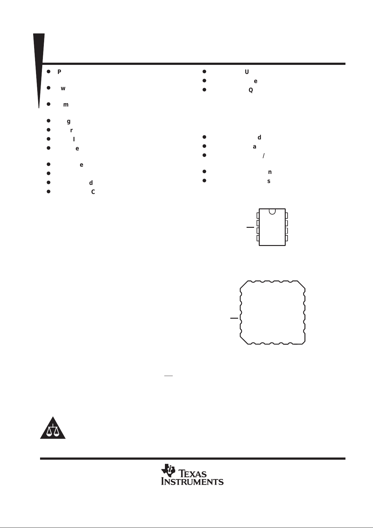
D, P, OR JG PACKAGE
(TOP VIEW)
1920132
17
18
16
15
14
1312119 10
5
4
6
7
8
NC
OUTB
NC
REFIN
NC
NC
SCLK
NC
CS
NC
NC
DINNCV
NC
OUTA
NC
AGND
NC
NC
FK PACKAGE
(TOP VIEW)
DD
On products compliant to MIL-PRF-38535, all parameters are tested
unless otherwise noted. On all other products, production
processing does not necessarily include testing of all parameters.
TLC5618, TLC5618A
PROGRAMMABLE DUAL 12-BIT DIGITAL-TO-ANALOG CONVERTERS
SLAS156E – JULY 1997 – REVISED SEPTEMBER 1999
2
POST OFFICE BOX 655303 • DALLAS, TEXAS 75265
description (continued)
The 8-terminal small-outline D package allows digital control of analog functions in space-critical applications.
The TLC5618C is characterized for operation from 0°C to 70°C. The TLC5618I is characterized for operation
from –40°C to 85°C. The TLC5618Q is characterized for operation from –40°C to 125°C. The TLC5618M is
characterized for operation from –55°C to 125°C.
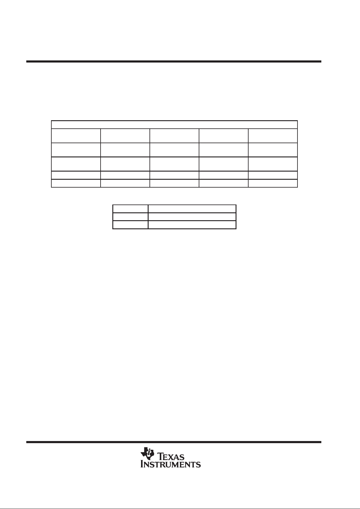
AVAILABLE OPTIONS
PACKAGE
T
A
SMALL OUTLINE
†
(D)
PLASTIC DIP
(P)
CERAMIC DIP
(JG)
20 PAD LCC
(FK)
0°C to 70°C
TLC5618CD
TLC5618ACD
TLC5618CP
TLC5618ACP
—
—
—
—
–40°C to 85°C
TLC5618ID
TLC5618AID
TLC5618IP
TLC5618AIP
—
—
—
—
–40°C to 125°C TLC5618AQD — — —
–55°C to 125°C — — TLC5618AMJG TLC5618AMFK
†
The D package is available in tape and reel by adding R to the part number
(e.g., TLC5618CDR)
DEVICE
COMPATIBILITY
TLC5618 SPI, QSPI and Microwire
TLC5618A TMS320Cxx, SPI, QSPI, and Microwire
TLC5618, TLC5618A
PROGRAMMABLE DUAL 12-BIT DIGITAL-TO-ANALOG CONVERTERS
SLAS156E – JULY 1997 – REVISED SEPTEMBER 1999
3
POST OFFICE BOX 655303 • DALLAS, TEXAS 75265
functional block diagram
_
+
DAC
12-Bit DAC Register Latch A
Power-Up
Reset
Control
Logic
16-Bit Shift Register
4
Program
Bits
12 Data Bits
(LSB) (MSB)
REFIN
AGND
CS
SCLK
DIN
OUT A
(Voltage Output)
_
+
RR
DAC A
×2
Double
Buffer
Latch
_
+
_
+
OUT B
(Voltage Output)
DAC B
DAC
R
×2
R
12-Bit DAC Register Latch B
7
4
6
5
3
2
1
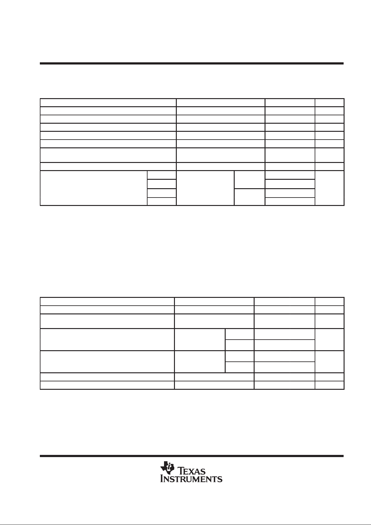
Terminal Functions
TERMINAL
NAME NO.
I/O
DESCRIPTION
AGND 5 Analog ground
CS 3 I Chip select, active low
DIN 1 I Serial data input
OUT A 4 O DAC A analog output
OUT B 7 O DAC B analog output
REFIN 6 I Reference voltage input
SCLK 2 I Serial clock input
V
DD
8 Positive power supply
TLC5618, TLC5618A
PROGRAMMABLE DUAL 12-BIT DIGITAL-TO-ANALOG CONVERTERS
SLAS156E – JULY 1997 – REVISED SEPTEMBER 1999
4
POST OFFICE BOX 655303 • DALLAS, TEXAS 75265
absolute maximum ratings over operating free-air temperature range (unless otherwise noted)
†
Supply voltage (VDD to AGND) 7 V. . . . . . . . . . . . . . . . . . . . . . . . . . . . . . . . . . . . . . . . . . . . . . . . . . . . . . . . . . . . . . .
Digital input voltage range to AGND – 0.3 V to VDD + 0.3 V. . . . . . . . . . . . . . . . . . . . . . . . . . . . . . . . . . . . . . . . . .
Reference input voltage range to AGND – 0.3 V to V
DD
+ 0.3 V. . . . . . . . . . . . . . . . . . . . . . . . . . . . . . . . . . . . . .
Output voltage at OUT from external source V
DD
+ 0.3 V. . . . . . . . . . . . . . . . . . . . . . . . . . . . . . . . . . . . . . . . . . . .
Continuous current at any terminal ±20 mA. . . . . . . . . . . . . . . . . . . . . . . . . . . . . . . . . . . . . . . . . . . . . . . . . . . . . . . .
Operating free-air temperature range, TA: TLC5618C, TLC5618AC 0°C to 70°C. . . . . . . . . . . . . . . . . . . . . . . .
TLC5618I, TLC5618AI –40°C to 85°C. . . . . . . . . . . . . . . . . . . . . . .
TLC5618AQ –40°C to 125°C. . . . . . . . . . . . . . . . . . . . . . . . . . . . . . .
TLC5618AM –55°C to 125°C. . . . . . . . . . . . . . . . . . . . . . . . . . . . . . .
Storage temperature range, T
stg
–65°C to 150°C. . . . . . . . . . . . . . . . . . . . . . . . . . . . . . . . . . . . . . . . . . . . . . . . . . .
Lead temperature 1,6 mm (1/16 inch) from case for 10 seconds 260°C. . . . . . . . . . . . . . . . . . . . . . . . . . . . . . .
†
Stresses beyond those listed under “absolute maximum ratings” may cause permanent damage to the device. These are stress ratings only, and
functional operation of the device at these or any other conditions beyond those indicated under “recommended operating conditions” is not
implied. Exposure to absolute-maximum-rated conditions for extended periods may affect device reliability.
DISSIPATION RATING TABLE
T
≤ 25°C DERATING FACTOR T
= 70°C T
= 85°C T
= 125°C
PACKAGE
A
POWER RATING ABOVE TA = 25°C
‡
A
POWER RATINGAPOWER RATINGAPOWER RATING
D 635 mW 5.08 mW/°C 407 mW 330 mW —
FK 1375 mW 11.00 mW/°C 880 mW 715 mW 275 mW
JG 1050 mW 8.40 mW/°C 672 mW 546 mW 210 mW
P 1202 mW 9.61 mW/°C 769 mW 625 mW —
‡
This is the inverse of the traditional Junction-to-Ambient thermal Resistance (RΘJA). Thermal Resistances are not production tested and are for
informational purposes only.
recommended operating conditions
MIN NOM MAX UNIT
Supply voltage, V
DD
4.5 5 5.5 V
High-level digital input voltage, V
IH
VDD = 5 V 0.7 V
DD
V
Low-level digital input voltage, V
IL
VDD = 5 V 0.3 V
DD
V
Reference voltage, V
ref
to REFIN terminal 2 2.048 VDD–1.1 V
Load resistance, R
L
2 kΩ
TLC5618C, TLC5618AC 0 70
p
p
TLC5618I, TLC5618AI –40 85
°
Operating free-air temperature, T
A
TLC5618AQ –40 125
°C
TLC5618AM –55 125
TLC5618, TLC5618A
PROGRAMMABLE DUAL 12-BIT DIGITAL-TO-ANALOG CONVERTERS
SLAS156E – JULY 1997 – REVISED SEPTEMBER 1999
5
POST OFFICE BOX 655303 • DALLAS, TEXAS 75265
electrical characteristics over recommended operating free-air temperature range, VDD = 5 V ±5%,
V
ref(REFIN)
= 2.048 V (unless otherwise noted)
static DAC specifications
PARAMETER TEST CONDITIONS MIN TYP MAX UNIT
Resolution 12 bits
Integral nonlinearity (INL), end point adjusted V
ref(REFIN)
= 2.048 V , See Note 1 ±4 LSB
Differential nonlinearity (DNL) V
ref(REFIN)
= 2.048 V , See Note 2 ±0.5 ± 1 LSB
E
ZS
Zero-scale error (offset error at zero scale) V
ref(REFIN)
= 2.048 V , See Note 3 ±12 mV
Zero-scale-error temperature coefficient V
ref(REFIN)
= 2.048 V , See Note 4 3 ppm/°C
E
G
Gain error V
ref(REFIN)
= 2.048 V , See Note 5 ±0.29
% of FS
voltage
Gain error temperature coefficient V
ref(REFIN)
= 2.048 V , See Note 6 1 ppm/°C
Zero scale
65
pp
Gain
Slo
w
65
PSRR
Power-su ly rejection ratio
Zero scale
See Notes 7 and 8
65
dB
Gain
Fast
65
NOTES: 1. The relative accuracy or integral nonlinearity (INL) sometimes referred to as linearity error, is the maximum deviation of the output
from the line between zero and full scale excluding the effects of zero code and full-scale errors.
2. The differential nonlinearity (DNL) sometimes referred to as differential error, is the difference between the measured and ideal 1
LSB amplitude change of any two adjacent codes. Monotonic means the output voltage changes in the same direction (or remains
constant) as a change in the digital input code.
3. Zero-scale error is the deviation from zero voltage output when the digital input code is zero.
4. Zero-scale-error temperature coefficient is given by: EZSTC = [EZS(T
max
) – EZS(T
min
)]/V
ref
× 106/(T
max
– T
min
).
5. Gain error is the deviation from the ideal output (V
ref
– 1 LSB) with an output load of 10 kΩ excluding the effects of the zero-error.
6. Gain temperature coefficient is given by: EGTC = [EG(T
max
) – EG (T
min
)]/V
ref
× 106/(T
max
– T
min
).
7. Zero-scale-error rejection ratio (EZS-RR) is measured by varying the VDD from 4.5 V to 5.5 V dc and measuring the proportion of
this signal imposed on the zero-code output voltage.
8. Gain-error rejection ratio (EG-RR) is measured by varying the VDD from 4.5 V to 5.5 V dc and measuring the proportion of this signal
imposed on the full-scale output voltage after subtracting the zero scale change.
OUT A and OUT B output specifications
PARAMETER TEST CONDITIONS MIN TYP MAX UNIT
V
O
Voltage output range RL = 10 kΩ 0 VDD–0.4 V
Output load regulation accuracy V
O(OUT)
= 4.096 V , RL = 2 kΩ ±0.29
% of FS
voltage
p
V
O(A OUT)
= VDD,
Fast 38
I
OSC(sink)
Out ut short circuit sink current
V
O(B OUT)
=
V
DD
,
Input code zero
Slow 23
mA
p
V
O(A OUT)
= 0 V,
Fast –54
I
OSC(
source
)
Out ut short circuit source current
V
O(B OUT)
= 0 V,
Full-scale code
Slow –29
mA
I
O(sink)
Output sink current V
O(OUT)
= 0.25 V 5 mA
I
O(source)
Output source current V
O(OUT)
= 4.2 V 5 mA
TLC5618, TLC5618A
PROGRAMMABLE DUAL 12-BIT DIGITAL-TO-ANALOG CONVERTERS
SLAS156E – JULY 1997 – REVISED SEPTEMBER 1999
6
POST OFFICE BOX 655303 • DALLAS, TEXAS 75265
electrical characteristics over recommended operating free-air temperature range, VDD = 5 V ±5%,
V
ref(REFIN)
= 2.048 V (unless otherwise noted) (continued)
reference input (REFIN)
PARAMETER TEST CONDITIONS MIN TYP MAX UNIT
VIInput voltage range 0 VDD–2 V
RiInput resistance 10 MΩ
CiInput capacitance 5 pF
Reference feedthrough REFIN = 1 Vpp at 1 kHz + 1.024 V dc (see Note 9) –60 dB
p
Slow 0.5
Reference input bandwidth (f
– 3
dB)
REFIN
= 0.2
V
pp
+ 1.
024 V dc
Fast 1
MH
z
NOTE 9: Reference feedthrough is measured at the DAC output with an input code = 000 hex and a V
ref(REFIN)
input = 1.024 V dc + 1 V
pp
at 1 kHz.
digital inputs (DIN, SCLK, CS)
PARAMETER TEST CONDITIONS MIN TYP MAX UNIT
I
IH
High-level digital input current VI = V
DD
±1 µA
I
IL
Low-level digital input current VI = 0 V ±1 µA
C
i
Input capacitance 8 pF
power supply
PARAMETER TEST CONDITIONS MIN TYP MAX
UNIT
pp
VDD = 5.5 V,
Slow 0.6 1
IDDPower supply current
No load
,
All inputs = 0 V or V
DD
Fast 1.6 2.5
mA
Power down supply current D13 = 0 (see Table 2) 1 µA
operating characteristics over recommended operating free-air temperature range, VDD = 5 V ±5%,
V
ref(REFIN)
= 2.048 V (unless otherwise noted)
analog output dynamic performance
PARAMETER TEST CONDITIONS MIN TYP MAX UNIT
p
p
CL = 100 pF,
V
ref(REFIN)
= 2.048 V ,
°
Slow 0.3 0.5
SR+Output slew rate, positive
R
L
= 10 kΩ,
Code 32 to Code 4096,
T
A
=
25°C
,
VO from 10% to 90%
Fast
2.4 3
V/µs
p
CL = 100 pF,
V
ref(REFIN)
= 2.048 V ,
°
Slow 0.15 0.25
SR–Output slew rate, negative
R
L
= 10 kΩ,
Code 4096 to Code 32,
T
A
=
25°C
,
VO from 10% to 90%
Fast
1.2 1.5
V/µs
p
To ±0.5 LSB,
CL = 100 pF,
Slow 12.5
tsOutput settling time
,
RL = 10 kΩ,
See Note 10
Fast
2.5
µ
s
Output settling time, To ±0.5 LSB,
CL = 100 pF,
Slow 2
t
s(c)
g,
code-to-code
,
RL = 10 kΩ,
See Note 11
Fast
2
µ
s
Glitch energy
DIN = All 0s to all 1s,
f
(SCLK)
= 100 kHz
CS = VDD,
5 nV–s
S/(N+D) Signal to noise + distortion
V
ref(REFIN)
= 1 Vpp at 1 kHz and 10 kHz + 1.024 V dc,
Input code = 10 0000 0000
78 dB
NOTES: 10. Settling time is the time for the output signal to remain within ±0.5 LSB of the final measured value for a digital input code change
of 020 hex to 3FF hex or 3FF hex to 020 hex.
11. Settling time is the time for the output signal to remain within ±0.5 LSB of the final measured value for a digital input code change
of one count.
TLC5618, TLC5618A
PROGRAMMABLE DUAL 12-BIT DIGITAL-TO-ANALOG CONVERTERS
SLAS156E – JULY 1997 – REVISED SEPTEMBER 1999
7
POST OFFICE BOX 655303 • DALLAS, TEXAS 75265
operating characteristics over recommended operating free-air temperature range, VDD = 5 V ±5%,
V
ref(REFIN)
= 2.048 V (unless otherwise noted) (continued)
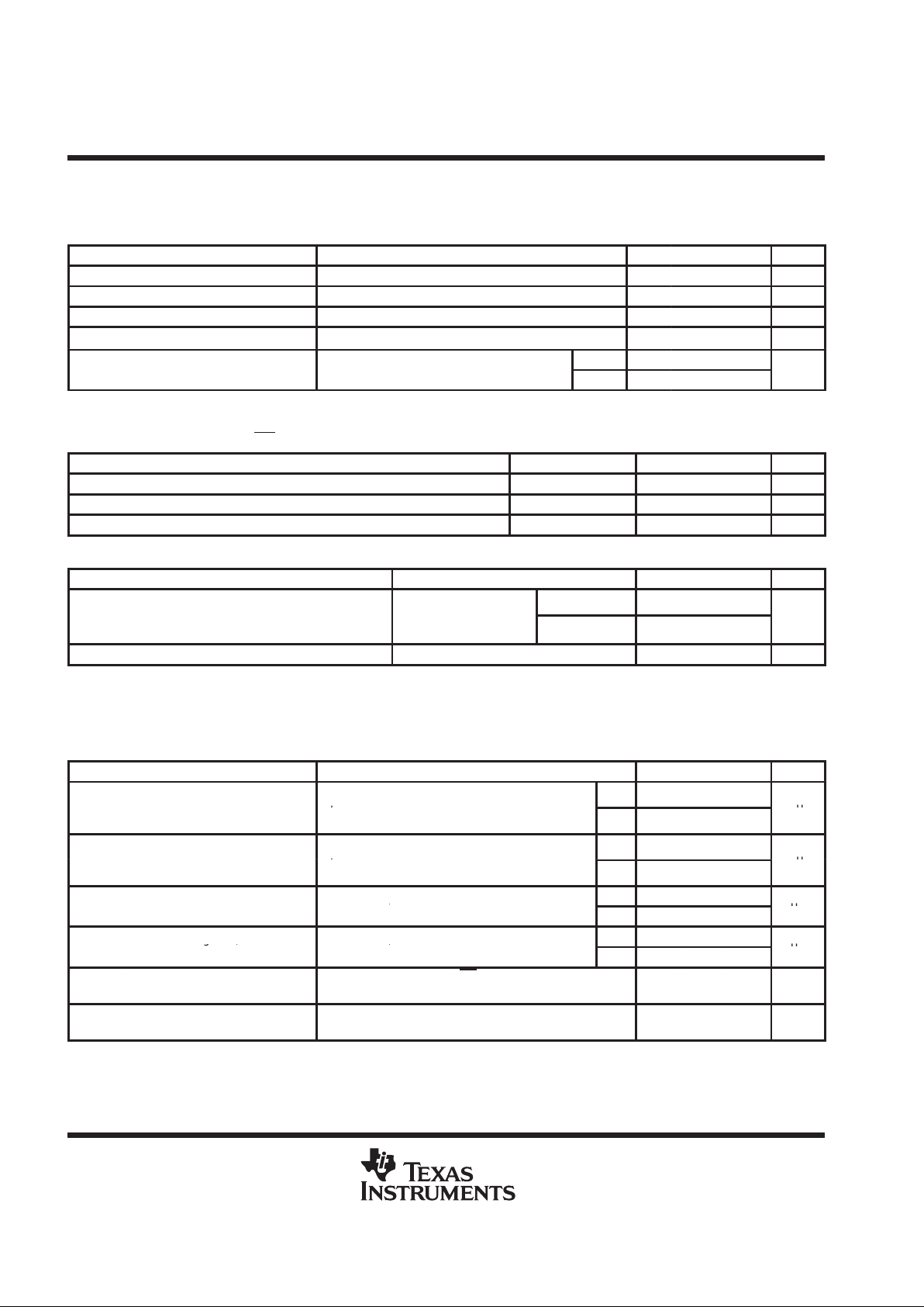
digital input timing requirements
MIN NOM MAX UNIT
t
su(DS)
Setup time, DIN before SCLK low 5 ns
t
h(DH)
Hold time, DIN valid after SCLK low 5 ns
t
su(CSS)
Setup time, CS low to SCLK low 5 ns
t
su(CS1)
Setup time, SCLK ↓ to CS ↑, external end-of-write 10 ns
t
su(CS2)
Setup time, SCLK ↑ to CS ↓, start of next write cycle 5 ns
t
w(CL)
Pulse duration, SCLK low 25 ns
t
w(CH)
Pulse duration, SCLK high 25 ns
t
d(CS1)
Delay time, CLK↑ to data disable (TLC5618A only) 5 20 ns
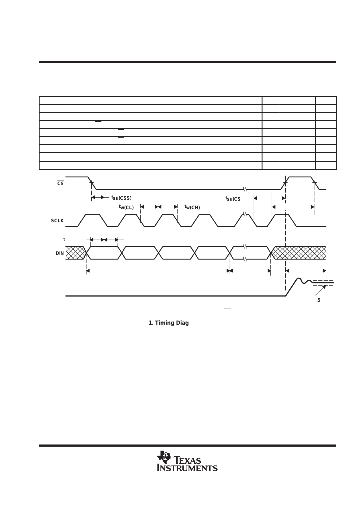
NOTE A: The input clock, applied at the SCLK terminal, should be inhibited high when CS is high to minimize clock feedthrough.
t
su(CSS)
t
w(CL)
t
w(CH)
CS
SCLK
DIN
t
su(DS)
t
h(DH)
D15 D14 D13 D12 D11 D0
t
s
DAC A/B
OUT
≤ Final Value ±0.5 LSB
(see Note A)
Program Bits (4)
DAC Data
Bits (12)
t
su(CS1)
t
su(CS2)
Figure 1. Timing Diagram for the TLC5618

TLC5618, TLC5618A
PROGRAMMABLE DUAL 12-BIT DIGITAL-TO-ANALOG CONVERTERS
SLAS156E – JULY 1997 – REVISED SEPTEMBER 1999
8
POST OFFICE BOX 655303 • DALLAS, TEXAS 75265
NOTE A: The input clock, applied at the SCLK terminal, should be inhibited high when CS is high to minimize clock feedthrough.
t
su(CSS)
t
w(CL)
t
w(CH)
CS
SCLK
DIN
t
su(DS)
t
h(DH)
D15 D14 D13 D12 D11 D0
t
s
DAC A/B
OUT
≤ Final Value ±0.5 LSB
(see Note A)
Program Bits (4)
DAC Data
Bits (12)
t
su(CS1)
t
su(CS2)
16th Falling Edge
t
d(CS1)
Internally Generated
Disable at This Time
Internal
Latch
Control
(see Note A)
Figure 2. Timing Diagram for TLC5618A Only

TLC5618, TLC5618A
PROGRAMMABLE DUAL 12-BIT DIGITAL-TO-ANALOG CONVERTERS
SLAS156E – JULY 1997 – REVISED SEPTEMBER 1999
9
POST OFFICE BOX 655303 • DALLAS, TEXAS 75265
TYPICAL CHARACTERISTICS
Figure 3
15
10
0
–5
012
Output Sink Current – mA
20
25
Output Load Voltage – V
OUTPUT SINK CURRENT (FAST MODE)
vs
OUTPUT LOAD VOLTAGE
30
3.5
5
35
40
1.50.5 2.5 3 4
4.5
VDD = 5 V,
Input Code = 0
Figure 4
–30
–20
–10
0
Output Source Current – mA
–40
–50
Output Load Voltage – V
OUTPUT SOURCE CURRENT (FAST MODE)
vs
OUTPUT LOAD VOLTAGE
–60
0 0.5 1
1.5 2
2.5 3 3.5 4 4.5
VDD = 5 V,
Input Code = 4095
Figure 5
10
5
0
–0
Output Sink Current – mA
15
20
Output Load Voltage – V
OUTPUT SINK CURRENT (SLOW MODE)
vs
OUTPUT LOAD VOLTAGE
25
0 0.5 1
1.5 2
2.5 3 3.5 4 4.5
VDD = 5 V,
Input Code = 0
Figure 6
–15
–10
–5
0
Output Source Current – mA
–20
–25
Output Load Voltage – V
OUTPUT SOURCE CURRENT (SLOW MODE)
vs
OUTPUT LOAD VOLTAGE
–30
0 0.5 1
1.5 2
2.5 3 3.5 4 4.5
VDD = 5 V,
Input Code = 4095

TLC5618, TLC5618A
PROGRAMMABLE DUAL 12-BIT DIGITAL-TO-ANALOG CONVERTERS
SLAS156E – JULY 1997 – REVISED SEPTEMBER 1999
10
POST OFFICE BOX 655303 • DALLAS, TEXAS 75265
TYPICAL CHARACTERISTICS
Figure 7
0.4
Supply Current – mA
1
1.4
SUPPLY CURRENT
vs
TEMPERATURE
1.2
0.8
0.6
0.2
0
–60 –40 –20 0 20 40 60 80 100 120 140
Temperature – °C
VDD = 5 V,
V
REFIN
= 2.048 V ,
TA = 25°C
Fast Mode
Slow Mode
1.6
Figure 8
–10
–15
–20
–30
100 1000
Relative Gain – dB
–5
0
f – Frequency – kHz
RELATIVE GAIN (FAST MODE)
vs
FREQUENCY
5
10 K
–25
VCC = 5 V,
V
REFIN
= 0.2 VPP + 2.048 Vdc,
TA = 25°C
Figure 9
–10
–15
–20
–30
100 1000
Relative Gain – dB
–5
0
f – Frequency – kHz
RELATIVE GAIN (SLOW MODE)
vs
FREQUENCY
5
10 K
–25
VCC = 5 V,
V
REFIN
= 0.2 VPP +2.048 Vdc,
TA = 25°C
–35
–40
Figure 10
80
75
70
65
110
THD – Total Harmonic Distortion – dB
85
90
f – Frequency – kHz
TOTAL HARMONIC DISTORTION (SLOW MODE)
vs
FREQUENCY
95
100

TLC5618, TLC5618A
PROGRAMMABLE DUAL 12-BIT DIGITAL-TO-ANALOG CONVERTERS
SLAS156E – JULY 1997 – REVISED SEPTEMBER 1999
11
POST OFFICE BOX 655303 • DALLAS, TEXAS 75265
TYPICAL CHARACTERISTICS
Figure 11
70
65
60
110
THD+N – Total Harmonic Distortion + Noise – dB
75
80
f – Frequency– kHz
TOTAL HARMONIC DISTORTION + NOISE (SLOW MODE)
vs
FREQUENCY
85
100
Figure 12
75
70
65
110
SNR – Signal-To-Noise Ratio – dB
80
f – Frequency– kHz
SIGNAL-TO-NOISE RATIO (SLOW MODE)
vs
FREQUENCY
85
100
Figure 13
85
80
75
110
THD – Total Harmonic Distortion – dB
90
f – Frequency – kHz
TOTAL HARMONIC DISTORTION (FAST MODE)
vs
FREQUENCY
95
100
Figure 14
75
70
65
110
THD+N – Total Harmonic Distortion + Noise – dB
80
f – Frequency – kHz
TOTAL HARMONIC DISTORTION + NOISE (FAST MODE)
vs
FREQUENCY
85
100

TLC5618, TLC5618A
PROGRAMMABLE DUAL 12-BIT DIGITAL-TO-ANALOG CONVERTERS
SLAS156E – JULY 1997 – REVISED SEPTEMBER 1999
12
POST OFFICE BOX 655303 • DALLAS, TEXAS 75265
TYPICAL CHARACTERISTICS
75
70
65
110
SNR – Signal-To-Noise Ratio – dB
80
f – Frequency – kHz
SIGNAL-TO-NOISE RATIO (FAST MODE)
vs
FREQUENCY
85
100
Figure 15

TLC5618, TLC5618A
PROGRAMMABLE DUAL 12-BIT DIGITAL-TO-ANALOG CONVERTERS
SLAS156E – JULY 1997 – REVISED SEPTEMBER 1999
13
POST OFFICE BOX 655303 • DALLAS, TEXAS 75265
TYPICAL CHARACTERISTICS
–0.6
1
0
–0.2
0.8
0.6
0.4
0.2
–0.4
–0.8
–1
Samples
500 2000 3000 40950 1000 1500 2500 3500
DNL – Differential Nonlinearity – LSB
Figure 16. Differential Nonlinearity With Input Code
–2
–1
–1.5
1
0.5
0
–0.5
–2.5
–3.0
Samples
500 2000 3000 40950 1000 1500 2500 3500
INL – Integral Nonlinearity – LSB
Figure 17. Integral Nonlinearity With Input Code

TLC5618, TLC5618A
PROGRAMMABLE DUAL 12-BIT DIGITAL-TO-ANALOG CONVERTERS
SLAS156E – JULY 1997 – REVISED SEPTEMBER 1999
14
POST OFFICE BOX 655303 • DALLAS, TEXAS 75265
APPLICATION INFORMATION
general function
The TLC5618 uses a resistor string network buffered with an op amp to convert 12-bit digital data to analog
voltage levels (see functional block diagram and Figure 18). The output is the same polarity as the reference
input (see Table 1).
The output code is given by: 2
ǒ
V
REFIN
Ǔ
CODE
4096
An internal circuit resets the DAC register to all 0s on power up.
_
+
Resistor
String
DAC
5 V
0.1 µF
AGND V
DD
OUT
REFIN
R
R
_
+
×2
DIN
CS
SCLK
Figure 18. TLC5618 Typical Circuit
Table 1. Binary Code Table (0 V to 2 V
REFIN
Output)
,
Gain = 2
INPUT OUTPUT
1111 1111 1111
2ǒV
REFIN
Ǔ
4095
4096
:
:
1000 0000 0001
2
ǒ
V
REFIN
Ǔ
2049
4096
1000 0000 0000
2ǒV
REFIN
Ǔ
2048
4096
+
V
REFIN
0111 1111 1111
2
ǒ
V
REFIN
Ǔ
2047
4096
:
:
0000 0000 0001
2
ǒ
V
REFIN
Ǔ
1
4096
0000 0000 0000
0 V

TLC5618, TLC5618A
PROGRAMMABLE DUAL 12-BIT DIGITAL-TO-ANALOG CONVERTERS
SLAS156E – JULY 1997 – REVISED SEPTEMBER 1999
15
POST OFFICE BOX 655303 • DALLAS, TEXAS 75265
APPLICATION INFORMATION
buffer amplifier
The output buffer has a rail-to-rail output with short circuit protection and can drive a 2-kΩ load with a 100-pF
load capacitance. Settling time is a software selectable 12.5 µs or 2.5 µs, typical to within ±0.5 LSB of final value.
external reference
The reference voltage input is buffered, which makes the DAC input resistance not code dependent. Therefore,
the REFIN input resistance is 10 MΩ and the REFIN input capacitance is typically 5 pF, independent of input
code. The reference voltage determines the DAC full-scale output.
logic interface
The logic inputs function with CMOS logic levels. Most of the standard high-speed CMOS logic families may
be used.
serial clock and update rate
Figure 1 shows the TLC5618 timing. The maximum serial clock rate is:
f
(SCLK)max
+
1
t
wǒCHǓmin
)
t
wǒCLǓmin
+
20 MHz
The digital update rate is limited by the chip-select period, which is:
t
p(CS)
+16 ǒt
wǒCH
Ǔ
)
t
wǒCL
Ǔ
Ǔ
)
t
suǒCS1
Ǔ
This equals an 810-ns or 1.23-MHz update rate. However, the DAC settling time to 12 bits limits the update rate
for full-scale input step transitions.
serial interface
When chip select (CS) is low, the input data is read into a 16-bit shift register with the input data clocked in, most
significant bit first. The falling edge of the SCLK input shifts the data into the input register.
The rising edge of CS then transfers the data to the DAC register. When CS is high, input data cannot be clocked
into the input register.
The 16 bits of data can be transferred with the sequence shown in Figure 19.
D15 D14 D13 D12 D11 12 Data Bits D0
Program Bits Data Bits
16 Bits
MSB (Input Word) MSB (Data) LSB (Data, Input Word)
Figure 19. Input Data Word Format

TLC5618, TLC5618A
PROGRAMMABLE DUAL 12-BIT DIGITAL-TO-ANALOG CONVERTERS
SLAS156E – JULY 1997 – REVISED SEPTEMBER 1999
16
POST OFFICE BOX 655303 • DALLAS, TEXAS 75265
APPLICATION INFORMATION
Table 2 shows the function of program bits D15 – D12.
Table 2. Program Bits D15 – D12 Function
PROGRAM BITS
D15 D14 D13 D12
DEVICE FUNCTION
1 X X X
Write to latch A with serial interface register data
and latch B updated with buffer latch data
0 X X 0 Write to latch B and double buffer latch
0 X X 1 Write to double buffer latch only
X 0 X X 12.5 µs settling time
X 1 X X 2.5 µs settling time
X X 0 X Powered-up operation
X X 1 X Power down mode
function of the latch control bits (D15 and D12)
Three data transfers are possible. All transfers occur immediately after CS goes high and are described in the
following sections.
latch A write, latch B update (D15 = high, D12 = X)
The serial interface register (SIR) data are written to latch A and the double buffer latch contents are written to
latch B. The double buffer contents are unaffected. This program bit condition allows simultaneous output
updates of both DACs.
Serial
Interface
Register
D12 = X
D15 = High
Latch A
Latch B
Double
Buffer Latch
To DAC A
To DAC B
Figure 20. Latch A Write, Latch B Update
latch B and double-buffer 1 write (D15 = low, D12 = low)
The SIR data are written to both latch B and the double buffer. Latch A is unaffected.
Serial
Interface
Register
D12 = Low
D15 = Low
Latch A
Latch B
Double
Buffer Latch
To DAC A
To DAC B
Figure 21. Latch B and Double-Buffer Write

TLC5618, TLC5618A
PROGRAMMABLE DUAL 12-BIT DIGITAL-TO-ANALOG CONVERTERS
SLAS156E – JULY 1997 – REVISED SEPTEMBER 1999
17
POST OFFICE BOX 655303 • DALLAS, TEXAS 75265
APPLICATION INFORMATION
double-buffer-only write (D15 = low, D12 = high)
The SIR data are written to the double buffer only. Latch A and B contents are unaffected.
Serial
Interface
Register
D12 = High
D15 = Low
Latch A
Latch B
Double
Buffer
To DAC A
To DAC B
Figure 22. Double-Buffer-Only Write
purpose and use of the double buffer
Normally only one DAC output can change after a write. The double buffer allows both DAC outputs to change
after a single write. This is achieved by the two following steps.
1. A double-buffer-only write is executed to store the new DAC B data without changing the DAC A and B
outputs.
2. Following the previous step, a write to latch A is executed. This writes the SIR data to latch A and also
writes the double-buffer contents to latch B. Thus both DACs receive their new data at the same time,
and so both DAC outputs begin to change at the same time.
Unless a double-buffer-only write is issued, the latch B and double-buffer contents are identical. Thus, following
a write to latch A or B with another write to latch A does not change the latch B contents.
operational examples
changing the latch A data from zero to full code
Assuming that latch A starts at zero code (e.g., after power-up), the latch can be filled with 1s by writing (bit D15
on the left, D0 on the right)
1X0X 1111 1111 1111
to the serial interface. Bit D14 can be zero to select slow mode or one to select fast mode. The other X can be
zero or one (don’t care).
The latch B contents and the DAC B output are not changed by this write unless the double-buffer contents are
different from the latch B contents. This can only be true if the last write was a double-buffer-only write.
changing the latch B data from zero to full code
Assuming that latch B starts at zero code (e.g., after power-up), the latch can be filled with 1s by writing (bit D15
on the left, D0 on the right).
0X00 1111 1111 1111
to the serial interface. Bit D14 can be zero to select slow mode or one to select fast mode. The data (bits D0
to D11) are written to both the double buffer and latch B.
The latch A contents and the DAC A output are not changed by this write.

TLC5618, TLC5618A
PROGRAMMABLE DUAL 12-BIT DIGITAL-TO-ANALOG CONVERTERS
SLAS156E – JULY 1997 – REVISED SEPTEMBER 1999
18
POST OFFICE BOX 655303 • DALLAS, TEXAS 75265
APPLICATION INFORMATION
double-buffered change of both DAC outputs
Assuming that DACs A and B start at zero code (e.g., after power-up), if DAC A is to be driven to mid-scale and
DAC B to full-scale, and if the outputs are to begin rising at the same time, this can be achieved as follows:
First,
0d01 1111 1111 1111
is written (bit D15 on the left, D0 on the right) to the serial interface. This loads the full-scale code into the double
buffer but does not change the latch B contents and the DAC B output voltage. The latch A contents and the
DAC A output are also unaffected by this write operation.
Changing from fast to slow or slow to fast mode changes the supply current which can glitch the outputs, and
so D14 (designated by d in the above data word) should be set to maintain the speed mode set by the previous
write.
Next,
1X0X 1000 0000 0000
is written (bit D15 on the left, D0 on the right) to the serial interface. Bit D14 can be zero to select slow mode
or one to select fast mode. The other X can be zero or one (don’t care). This writes the mid-scale code
(100000000000) to latch A and also copies the full-scale code from the double buffer to latch B. Both DAC
outputs thus begin to rise after the second write.
DSP serial interface
Utilizing a simple 3-wire serial interface shown in Figure 23, the TLC5618A can be interfaced to TMS320
compatible serial ports. The 5618A has an internal state machine that will count 16 clocks after receiving a falling
edge of CS
and then disable further clocking in of data until the next falling edge is received on CS. Therefore
CS can be connected directly to the FS pins of the serial port and only the leading falling edge of the DSP will
be used to start the write process. The TLC5618A is designed to be used with the TMS320Cxx DSP in burst
mode serial port transmit operation.

TLC5618, TLC5618A
PROGRAMMABLE DUAL 12-BIT DIGITAL-TO-ANALOG CONVERTERS
SLAS156E – JULY 1997 – REVISED SEPTEMBER 1999
19
POST OFFICE BOX 655303 • DALLAS, TEXAS 75265
APPLICATION INFORMATION
SCLK
DIN
CS
TLC5618A
CLKX
DX
FSX
TMS320C203
DSP
V
CC
OUT A
OUT B
GND
REFIN
2.5 V dc
FSR
To Source
Ground
Analog
Output
Analog
Output
CLKR
Figure 23. Interfacing The TLC5618A to the TMS320C203 DSP
general serial interface
Both the TLC5618 and TLC5618A are compatible with SPI, QSPI, or Microwire serial standards. The hardware
connections are shown in Figures 24 and 25. The TLC5618A has an internal state machine that will count 16
clocks after the falling edge of CS and then internally disable the device. The internal edge is ORed together
with CS so that the rising edge can be provided to CS prior to the occurrence of the internal edge to also disable
the device.
The SPI and Microwire interfaces transfer data in 8-bit bytes, therefore, two write cycles are required to input
data to the DAC. The QSPI interface, which has a variable input data length from 8 to 16 bits, can load the DAC
input register in one write cycle.
SCLK
DIN
CS
TLC5618,
TLC5618A
SK
SO
I/O
Microwire
Port
Figure 24. Microwire Connection

TLC5618, TLC5618A
PROGRAMMABLE DUAL 12-BIT DIGITAL-TO-ANALOG CONVERTERS
SLAS156E – JULY 1997 – REVISED SEPTEMBER 1999
20
POST OFFICE BOX 655303 • DALLAS, TEXAS 75265
APPLICATION INFORMATION
SCLK
DIN
CS
TLC5618,
TLC5618A
SCK
MOSI
I/O
SPI/QSPI
Port
CPOL = 1, CPHA = 0
Figure 25. SPI/QSPI Connection
linearity, offset, and gain error using single end supplies
When an amplifier is operated from a single supply , the voltage offset can still be either positive or negative. With
a positive offset, the output voltage changes on the first code change. With a negative offset the output voltage
may not change with the first code depending on the magnitude of the offset voltage.
The output amplifier attempts to drive the output to a negative voltage. However, because the most negative
supply rail is ground, the output cannot drive below ground and clamps the output at 0 V.
The output voltage then remains at zero until the input code value produces a sufficient positive output voltage
to overcome the negative offset voltage, resulting in the transfer function shown in Figure 26.
DAC Code
Output
Voltage
0 V
Negative
Offset
Figure 26. Effect of Negative Offset (Single Supply)
This offset error, not the linearity error , produces this breakpoint. The transfer function would have followed the
dotted line if the output buffer could drive below the ground rail.
For a DAC, linearity is measured between zero-input code (all inputs 0) and full-scale code (all inputs 1) after
offset and full scale are adjusted out or accounted for in some way . However , single supply operation does not
allow for adjustment when the offset is negative due to the breakpoint in the transfer function. So the linearity
is measured between full-scale code and the lowest code that produces a positive output voltage. The code is
calculated from the maximum specification for the negative offset.

TLC5618, TLC5618A
PROGRAMMABLE DUAL 12-BIT DIGITAL-TO-ANALOG CONVERTERS
SLAS156E – JULY 1997 – REVISED SEPTEMBER 1999
21
POST OFFICE BOX 655303 • DALLAS, TEXAS 75265
APPLICATION INFORMATION
power-supply bypassing and ground management
Printed-circuit boards that use separate analog and digital ground planes offer the best system performance.
Wire-wrap boards do not perform well and should not be used. The two ground planes should be connected
together at the low-impedance power-supply source. The best ground connection may be achieved by
connecting the DAC AGND terminal to the system analog ground plane making sure that analog ground
currents are well-managed.
A 0.1-µF ceramic bypass capacitor should be connected between V
DD
and AGND and mounted with short leads
as close as possible to the device. Use of ferrite beads may further isolate the system analog and digital power
supplies.
Figure 27 shows the ground plane layout and bypassing technique.
0.1 µF
Analog Ground Plane
1
2
3
4
8
7
6
5
Figure 27. Power-Supply Bypassing
saving power
Setting the DAC register to all 0s minimizes power consumption by the reference resistor array and the output
load when the system is not using the DAC.
ac considerations/analog feedthrough
Higher frequency analog input signals may couple to the output through internal stray capacitance. Analog
feedthrough is tested by holding CS high, setting the DAC code to all 0s, sweeping the frequency applied to
REFIN, and monitoring the DAC output.

TLC5618, TLC5618A
PROGRAMMABLE DUAL 12-BIT DIGITAL-TO-ANALOG CONVERTERS
SLAS156E – JULY 1997 – REVISED SEPTEMBER 1999
22
POST OFFICE BOX 655303 • DALLAS, TEXAS 75265
MECHANICAL DATA
D (R-PDSO-G**) PLASTIC SMALL-OUTLINE PACKAGE
14 PIN SHOWN
4040047/D 10/96
0.228 (5,80)
0.244 (6,20)
0.069 (1,75) MAX
0.010 (0,25)
0.004 (0,10)
1
14
0.014 (0,35)
0.020 (0,51)
A
0.157 (4,00)
0.150 (3,81)
7
8
0.044 (1,12)
0.016 (0,40)
Seating Plane
0.010 (0,25)
PINS **
0.008 (0,20) NOM
A MIN
A MAX
DIM
Gage Plane
0.189
(4,80)
(5,00)
0.197
8
(8,55)
(8,75)
0.337
14
0.344
(9,80)
16
0.394
(10,00)
0.386
0.004 (0,10)
M
0.010 (0,25)
0.050 (1,27)
0°–8°
NOTES: A. All linear dimensions are in inches (millimeters).
B. This drawing is subject to change without notice.
C. Body dimensions do not include mold flash or protrusion, not to exceed 0.006 (0,15).
D. Falls within JEDEC MS-012

TLC5618, TLC5618A
PROGRAMMABLE DUAL 12-BIT DIGITAL-TO-ANALOG CONVERTERS
SLAS156E – JULY 1997 – REVISED SEPTEMBER 1999
23
POST OFFICE BOX 655303 • DALLAS, TEXAS 75265
MECHANICAL DATA
FK (S-CQCC-N**) LEADLESS CERAMIC CHIP CARRIER
4040140/C 11/95
28 TERMINALS SHOWN
B
0.358
(9,09)
MAX
(11,63)
0.560
(14,22)
0.560
0.458
0.858
(21,8)
1.063
(27,0)
(14,22)
A
NO. OF
MINMAX
0.358
0.660
0.761
0.458
0.342
(8,69)
MIN
(11,23)
(16,26)
0.640
0.740
0.442
(9,09)
(11,63)
(16,76)
0.962
1.165
(23,83)
0.938
(28,99)
1.141
(24,43)
(29,59)
(19,32)(18,78)
**
20
28
52
44
68
84
0.020 (0,51)
TERMINALS
0.080 (2,03)
0.064 (1,63)
(7,80)
0.307
(10,31)
0.406
(12,58)
0.495
(12,58)
0.495
(21,6)
0.850
(26,6)
1.047
0.045 (1,14)
0.045 (1,14)
0.035 (0,89)
0.035 (0,89)
0.010 (0,25)
12
1314151618 17
11
10
8
9
7
5
432
0.020 (0,51)
0.010 (0,25)
6
12826 27
19
21
B SQ
A SQ
22
23
24
25
20
0.055 (1,40)
0.045 (1,14)
0.028 (0,71)
0.022 (0,54)
0.050 (1,27)
NOTES: A. All linear dimensions are in inches (millimeters).
B. This drawing is subject to change without notice.
C. This package can be hermetically sealed with a metal lid.
D. The terminals are gold-plated.
E. Falls within JEDEC MS-004

MECHANICAL DATA
MCER001A – JANUARY 1995 – REVISED JANUARY 1997
24
POST OFFICE BOX 655303 • DALLAS, TEXAS 75265
MECHANICAL DATA
JG (R-GDIP-T8) CERAMIC DUAL-IN-LINE
0.310 (7,87)
0.290 (7,37)
0.014 (0,36)
0.008 (0,20)
Seating Plane
4040107/C 08/96
5
4
0.065 (1,65)
0.045 (1,14)
8
1
0.020 (0,51) MIN
0.400 (10,16)
0.355 (9,00)
0.015 (0,38)
0.023 (0,58)
0.063 (1,60)
0.015 (0,38)
0.200 (5,08) MAX
0.130 (3,30) MIN
0.245 (6,22)
0.280 (7,11)
0.100 (2,54)
0°–15°
NOTES: A. All linear dimensions are in inches (millimeters).
B. This drawing is subject to change without notice.
C. This package can be hermetically sealed with a ceramic lid using glass frit.
D. Index point is provided on cap for terminal identification.
E. Falls within MIL STD 1835 GDIP1-T8

MECHANICAL DATA
MCER001A – JANUARY 1995 – REVISED JANUARY 1997
25
POST OFFICE BOX 655303 • DALLAS, TEXAS 75265
MECHANICAL DATA
P (R-PDIP-T8) PLASTIC DUAL-IN-LINE PACKAGE
4040082/B 03/95
0.310 (7,87)
0.290 (7,37)
0.010 (0,25) NOM
0.400 (10,60)
0.355 (9,02)
58
41
0.020 (0,51) MIN
0.070 (1,78) MAX
0.240 (6,10)
0.260 (6,60)
0.200 (5,08) MAX
0.125 (3,18) MIN
0.015 (0,38)
0.021 (0,53)
Seating Plane
M
0.010 (0,25)
0.100 (2,54)
0°–15°
NOTES: A. All linear dimensions are in inches (millimeters).
B. This drawing is subject to change without notice.
C. Falls within JEDEC MS-001

IMPORTANT NOTICE
T exas Instruments and its subsidiaries (TI) reserve the right to make changes to their products or to discontinue
any product or service without notice, and advise customers to obtain the latest version of relevant information
to verify, before placing orders, that information being relied on is current and complete. All products are sold
subject to the terms and conditions of sale supplied at the time of order acknowledgement, including those
pertaining to warranty, patent infringement, and limitation of liability.
TI warrants performance of its semiconductor products to the specifications applicable at the time of sale in
accordance with TI’s standard warranty. Testing and other quality control techniques are utilized to the extent
TI deems necessary to support this warranty. Specific testing of all parameters of each device is not necessarily
performed, except those mandated by government requirements.
CERT AIN APPLICATIONS USING SEMICONDUCTOR PRODUCTS MAY INVOLVE POTENTIAL RISKS OF
DEATH, PERSONAL INJURY, OR SEVERE PROPERTY OR ENVIRONMENTAL DAMAGE (“CRITICAL
APPLICATIONS”). TI SEMICONDUCTOR PRODUCTS ARE NOT DESIGNED, AUTHORIZED, OR
WARRANTED TO BE SUITABLE FOR USE IN LIFE-SUPPORT DEVICES OR SYSTEMS OR OTHER
CRITICAL APPLICATIONS. INCLUSION OF TI PRODUCTS IN SUCH APPLICA TIONS IS UNDERSTOOD T O
BE FULLY AT THE CUSTOMER’S RISK.
In order to minimize risks associated with the customer’s applications, adequate design and operating
safeguards must be provided by the customer to minimize inherent or procedural hazards.
TI assumes no liability for applications assistance or customer product design. TI does not warrant or represent
that any license, either express or implied, is granted under any patent right, copyright, mask work right, or other
intellectual property right of TI covering or relating to any combination, machine, or process in which such
semiconductor products or services might be or are used. TI’s publication of information regarding any third
party’s products or services does not constitute TI’s approval, warranty or endorsement thereof.
Copyright 1999, Texas Instruments Incorporated
 Loading...