

TLC5602C, TLC5602M
VIDEO 8-BIT DIGITAL-TO-ANALOG CONVERTERS
SLAS023C – FEBRUARY 1989 – REVISED MAY 1995
1
POST OFFICE BOX 655303 • DALLAS, TEXAS 75265
D
8-Bit Resolution
D
±0.2% Linearity
D
Maximum Conversion Rate
30 MHz Typ
20 MHz Min
D
Analog Output Voltage Range
V
DD
to VDD –1 V
D
TTL Digital Input Voltage
D
5-V Single Power-Supply Operation
D
Low Power Consumption...80 mW Typ
D
Interchangeable With Fujitsu MB40778
description
The TLC5602x devices are low-power, ultra-high-speed video, digital-to-analog converters that use the
LinEPIC 1-µm CMOS process. The TLC5602x converts digital signals to analog signals at a sampling rate
of dc to 20 MHz. Because of high-speed operation, the TLC5602x devices are suitable for digital video
applications such as digital television, video processing with a computer, and radar-signal processing.
The TLC5602C is characterized for operation from 0°C to 70°C. The TLC5602M is characterized over the full
military temperature range of –55°C to 125°C.
1
2
3
4
5
6
7
8
9
18
17
16
15
14
13
12
11
10
DGTL GND
DGTL V
DD
COMP
REF
ANLG V
DD1
A OUT
ANLG V
DD2
DGTL V
DD
ANLG GND
D0 (LSB)
D1
D2
D3
D4
D5
D6
D7 (MSB)
CLK
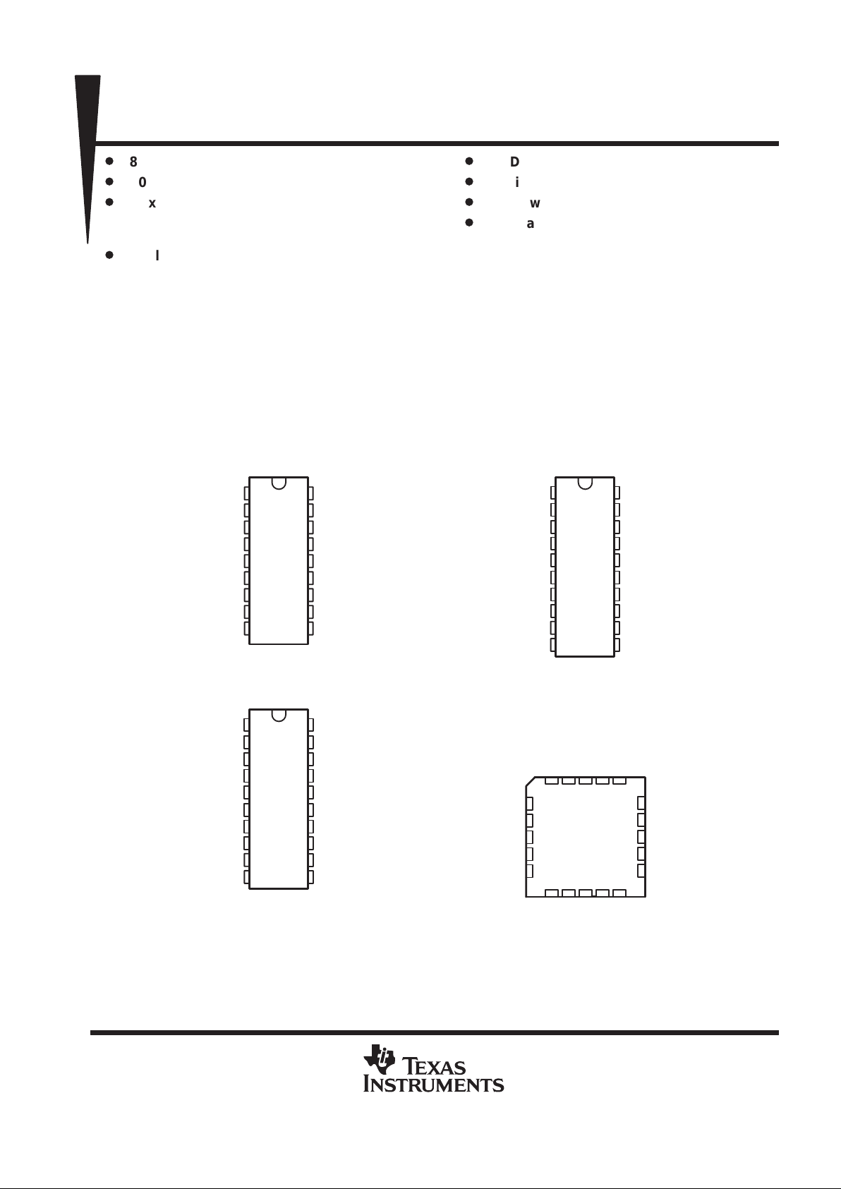
N PACKAGE
(TOP VIEW)
1
2
3
4
5
6
7
8
9
10
20
19
18
17
16
15
14
13
12
11
DGTL GND
DGTL V
DD
COMP
REF
ANLG V
DD1
A OUT
NC
ANLG V
DD2
DGTL V
DD
ANLG GND
NC
D0 (LSB)
D1
D2
D3
D4
D5
D6
D7 (MSB)
CLK
NC—No internal connection
DW PACKAGE
(TOP VIEW)
1
2
3
4
5
6
7
8
9
10
20
19
18
17
16
15
14
13
12
11
NC
DGTL GND
DGTL V
DD
COMP
REF
ANLG V
DD1
A OUT
ANLG V
DD2
DGTL V
DD
ANLG GND
NC
D0 (LSB)
D1
D2
D3
D4
D5
D6
D7 (MSB)
CLK
J PACKAGE
(TOP VIEW)
3212019
910111213
4
5
6
7
8
18
17
16
15
14
D1
D2
D3
D4
D5
COMP
REF
ANLG V
DD1
A OUT
ANLG V
DD2
FK PACKAGE
(TOP VIEW)
DGTL V
DGTL GND
NC
D7 (MSB)
D6
NC
D0 (LSB)
ANLG GND
CLK
DD
DGTL V
DD
Copyright 1995, Texas Instruments Incorporated
PRODUCTION DATA information is current as of publication date.
Products conform to specifications per the terms of Texas Instruments
standard warranty. Production processing does not necessarily include
testing of all parameters.
LinEPIC is a trademark of Texas Instruments Incorporated.
TLC5602C, TLC5602M
VIDEO 8-BIT DIGITAL-TO-ANALOG CONVERTERS
SLAS023C – FEBRUARY 1989 – REVISED MAY 1995
2
POST OFFICE BOX 655303 • DALLAS, TEXAS 75265
AVAILABLE OPTIONS
PACKAGE
T
A
WIDE-BODY SMALL OUTLINE
(DW)
CERAMIC CHIP CARRIER
(FK)
CERAMIC DIP
(J)
PLASTIC DIP
(N)
0°C to 70°C TLC5602CDW TLC5602CN
–55°C to 125°C TLC5602MFK TLC5602MJ
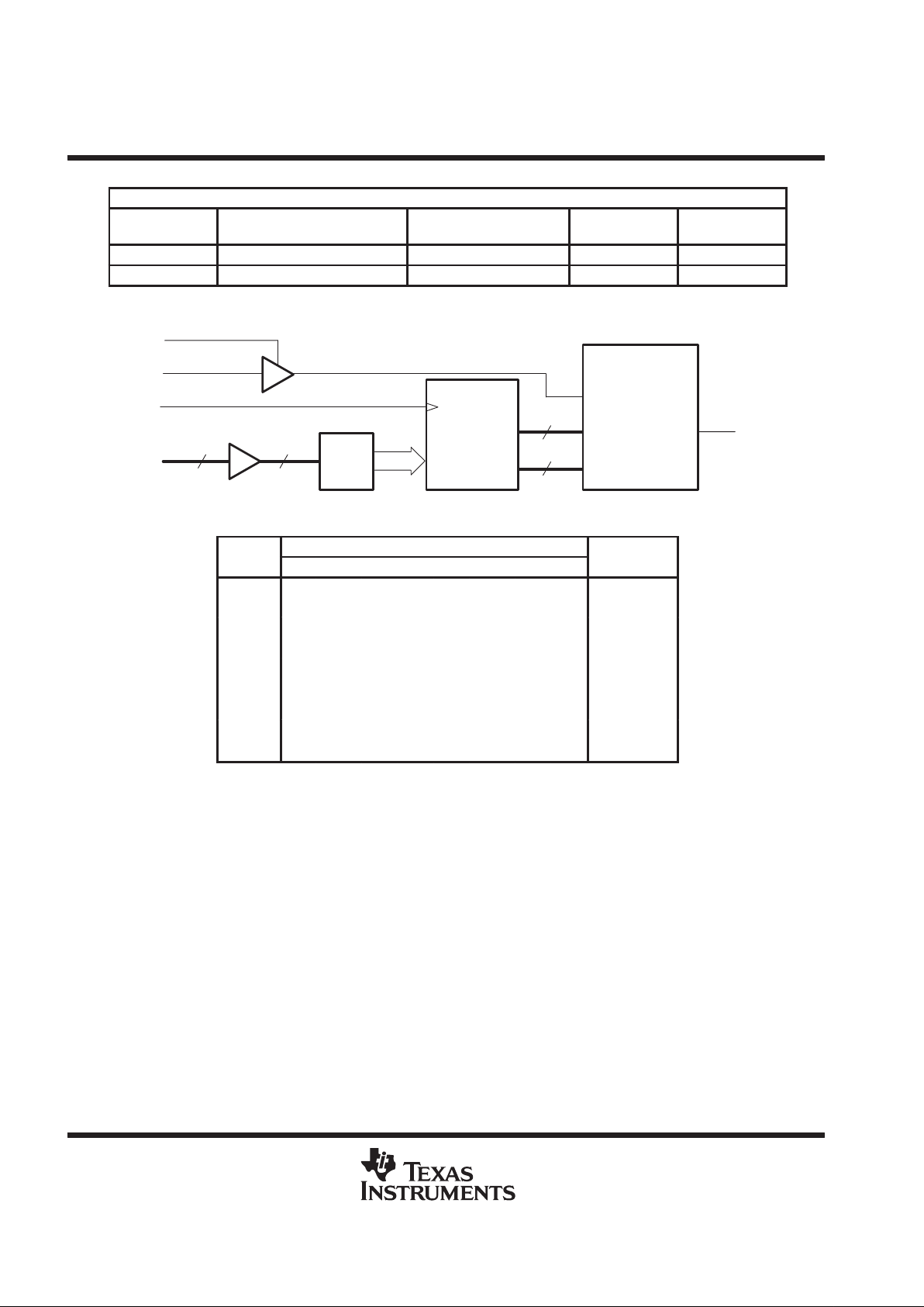
functional block diagram
Buffer
Driver With
Register
Current
Switches
With
Register
Decode
COMP
REF
CLK
D7–D0
A OUT
88
3
63
I x 4
I x 1
FUNCTION TABLE
DIGITAL INPUTS
OUTPUT
STEP
D7 D6 D5 D4 D3 D2 D1 D0
VOLTAGE
†
0 L L L L L L L L 3.980 V
1 L L L L L L L H 3.984 V
| ||
127 L H H H H H H H 4.488 V
128 H L L L L L L L 4.492 V
129 H L L L L L L H 4.496 V
| ||
254 H H H H H H H L 4.996 V
255 H H H H H H H H 5.000 V
†
VDD = 5 V and V
ref
= 4.02 V
TLC5602C, TLC5602M
VIDEO 8-BIT DIGITAL-TO-ANALOG CONVERTERS
SLAS023C – FEBRUARY 1989 – REVISED MAY 1995
3
POST OFFICE BOX 655303 • DALLAS, TEXAS 75265
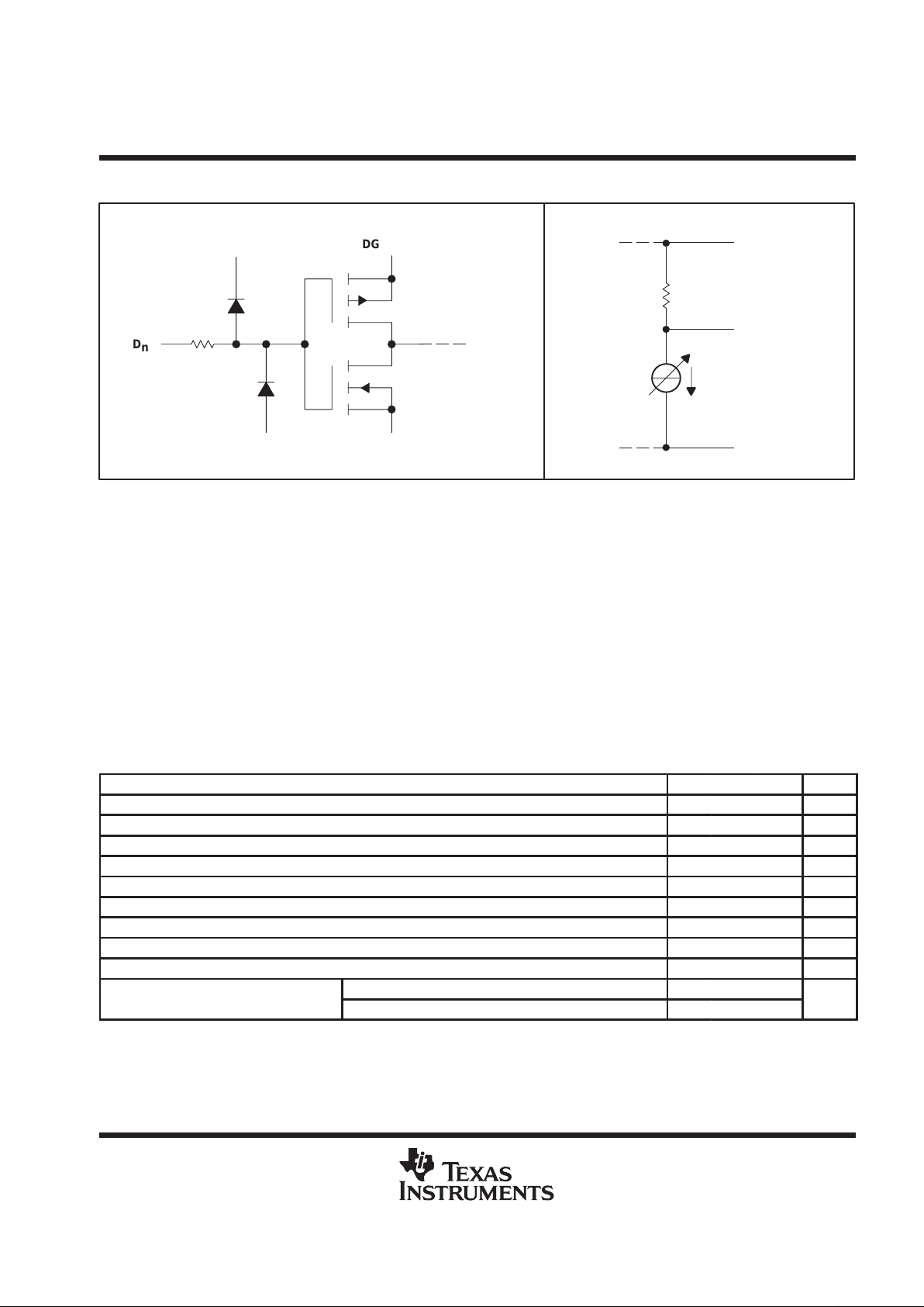
schematics of equivalent input and output
EQUIVALENT OF ANALOG OUTPUTEQUIVALENT OF EACH DIGITAL INPUT
ANLG
‡
GND
A OUT
80 Ω
ANLG V
DD1
D
n
DGTL V
DD
ANLG
‡
GND
DGTL
‡
GND
DGTL V
DD
‡
ANLG GND and DGTL GND do not connect internally and should be tied together as close to the device terminals as possible.
absolute maximum ratings over operating free-air temperature range (unless otherwise noted)
†
Supply voltage range, ANLG V
DD
, DGTL VDD –0.5 V to 7 V. . . . . . . . . . . . . . . . . . . . . . . . . . . . . . . . . . . . . . . . .
Digital input voltage range, V
I
–0.5 V to 7 V. . . . . . . . . . . . . . . . . . . . . . . . . . . . . . . . . . . . . . . . . . . . . . . . . . . . . . . .
Analog reference voltage range, V
ref
V
DD
– 1.7 V to VDD + 0.5 V. . . . . . . . . . . . . . . . . . . . . . . . . . . . . . . . . . .
Operating free-air temperature range, T
A
: TLC5602C 0°C to 70°C. . . . . . . . . . . . . . . . . . . . . . . . . . . . . . . . . . .
TLC5602M –55°C to 125°C. . . . . . . . . . . . . . . . . . . . . . . . . . . . . . .
Storage temperature range, T
stg
–65°C to 150°C. . . . . . . . . . . . . . . . . . . . . . . . . . . . . . . . . . . . . . . . . . . . . . . . . .
Lead temperature 1,6 mm (1/16 inch) from case for 10 seconds 260°C. . . . . . . . . . . . . . . . . . . . . . . . . . . . . . .
†
Stresses beyond those listed under “absolute maximum ratings” may cause permanent damage to the device. These are stress ratings only, and
functional operation of the device at these or any other conditions beyond those indicated under “recommended operating conditions” is not
implied. Exposure to absolute-maximum-rated conditions for extended periods may affect device reliability.
recommended operating conditions
MIN NOM MAX UNIT
Supply voltage, V
DD
4.75 5 5.25 V
Analog reference voltage, V
ref
3.8 4 4.2 V
High-level input voltage, V
IH
2 V
Low-level input voltage, V
IL
0.8 V
Pulse duration, CLK high or low, t
w
25 ns
Setup time, data before CLK↑, t
su
16.5 ns
Hold time, data after CLK↑, t
h
12.5 ns
Phase compensation capacitance, C
comp
(see Note 1) 1 µF
Load resistance, R
L
75k Ω
p
p
TLC5602C 0 70
°
Operating free-air temperature,T
A
TLC5602M –55 125
°C
NOTE 1: The phase compensation capacitor should be connected between COMP and ANLG GND.

TLC5602C, TLC5602M
VIDEO 8-BIT DIGITAL-TO-ANALOG CONVERTERS
SLAS023C – FEBRUARY 1989 – REVISED MAY 1995
4
POST OFFICE BOX 655303 • DALLAS, TEXAS 75265
electrical characteristics over recommended ranges of supply voltage and operating free-air
temperature (unless otherwise noted)
PARAMETER TEST CONDITIONS MIN TYP
‡
MAX UNIT
I
IH
High-level input current
Digital
VI = 5 V ±1 µA
I
IL
Low-level input current
g
inputs
VI = 0 V ±1 µA
I
ref
Input reference current V
ref
= 4 V 10 µA
V
FS
Full-scale analog output voltage VDD = 5 V, V
ref
= 4.02 V VDD–15 VDDVDD+15 mV
TLC5602C 3.919 3.98 4.042
V
ZS
Zero-scale analog output voltage
VDD = 5 V,
§
V
ref
= 4.02 V ,
TLC5602M
3.919 3.98 4.042
V
T
A
=
full range
§
TLC5602M 3.919 3.98 4.062
p
TA = 25°C TLC5602C
roOutput resistance
TA = full range
§
TLC5602M
6080120
Ω
C
i
Input capacitance f
clock
= 1 MHz, TA = 25°C 15 pF
I
DD
Supply current f
clock
= 20 MHz, V
ref
= VDD–0.95 V 16 25 mA
‡
All typical values are at VDD = 5 V and TA = 25°C.
§
Full range for the TLC5602C is 0°C to 70°C, and full range for the TLC5602M is –55°C to 125°C.
operating characteristics over recommended ranges of supply voltage and operating free-air
temperature (unless otherwise noted)
PARAMETER TEST CONDITIONS MIN TYP†MAX UNIT
TA = full range
‡
TLC5602C ±0.2%
E
L(adj)
Linearity error, best-straight-line
TA = 25°C
±0.2%
(j)
TA = full range
‡
TLC5602M
±0.4%
E
L
Linearity error, end point ±0.15%
E
D
Linearity error, differential ±0.2%
G
diff
Differential gain
NTSC 40-IRE modulated ramp,
0.7%
f
diff
Differential phase
,
f
clock
= 14.3 MHz, ZL ≥ 75 kΩ
0.4°
t
pd
Propagation delay time, CLK to analog output CL = 10 pF 25 ns
t
s
Settling time to within 1/2 LSB CL = 10 pF 30 ns
†
All typical values are at VDD = 5 V and TA = 25°C.
‡
Full range for the TLC5602C is 0°C to 70°C, and full range for the TLC5602M is –55°C to 125°C.

TLC5602C, TLC5602M
VIDEO 8-BIT DIGITAL-TO-ANALOG CONVERTERS
SLAS023C – FEBRUARY 1989 – REVISED MAY 1995
5
POST OFFICE BOX 655303 • DALLAS, TEXAS 75265
PARAMETER MEASUREMENT INFORMATION
t
h
t
su
t
w
t
pd
50%50%
±1/2 LSB
50%
A OUT
CLK
D0–D7
ÏÏ
t
s
t
w
50% 50% 50%
Figure 1. Voltage Waveforms

TLC5602C, TLC5602M
VIDEO 8-BIT DIGITAL-TO-ANALOG CONVERTERS
SLAS023C – FEBRUARY 1989 – REVISED MAY 1995
6
POST OFFICE BOX 655303 • DALLAS, TEXAS 75265
TYPICAL CHARACTERISTICS
Figure 2
5
4.996
4.496
4.492
4.488
3.988
3.984
3.98
00000000
00000001
00001110
Digital Input Code
01111111
10000000
10000001
11111111
11111110
4.992
VDD = 5 V
V
ref
= 4.02 V
Step 2
Step 1
Step 127
Step 128
Step 129
Step 253
Step 254
IDEAL CONVERSION CHARACTERISTICS
V
O
–
A
na
l
og
O
u
t
pu
t
V
o
lt
age –
V
Figure 3
00000000
00000001
00001110
01111111
10000000
10000001
11111111
11111110
VDD = 5 V
V
ref
= 4.02 V
5
4.996
4.496
4.492
4.488
3.988
3.984
3.98
Digital Input Code
4.992
E
L127
E
L128
E
L129
E
L254
E
L253
E
L0
E
L2
V
ZS
Best-Fit Straight Line
BEST-STRAIGHT-LINE LINEARITY ERROR
V
O
– Analog Output Voltage – V
E
L1
V
FS
E
L255
3.96
3.95
3.93
3.92
– 55 – 35 – 15 5 25 45 65
3.97
3.99
ZERO-SCALE OUTPUT VOLTAGE
vs
FREE-AIR TEMPERATURE
4
85 105
3.94
3.98
4.01
4.02
VDD = 5 V
V
ref
= 4.02 V
See Note A
TA – Free-Air Temperature – °C
V
ZS
– Zero-Scale Output Voltage – V
125
NOTE A: V
ref
is relative to ANLG GND. VDD is the voltage between
ANLG VDD and DGTL VDD tied together and ANLG GND
and DGTL GND tied together.
Figure 4
70
65
55
50
75
85
90
60
80
95
100
– Output Resistance –
OUTPUT RESISTANCE
vs
FREE-AIR TEMPERATURE
TA – Free-Air Temperature – °C
Ωr
o
– 55 – 35 – 15 5 25 45 65 85 105 125
VDD = 5 V
VDD = VO = 0.5 V
Data Input = FF
Figure 5

TLC5602C, TLC5602M
VIDEO 8-BIT DIGITAL-TO-ANALOG CONVERTERS
SLAS023C – FEBRUARY 1989 – REVISED MAY 1995
7
POST OFFICE BOX 655303 • DALLAS, TEXAS 75265
TYPICAL CHARACTERISTICS
18
16
SUPPLY CURRENT
vs
FREE-AIR TEMPERATURE
20
17
19
21
TA – Free-Air Temperature – °C
I
DD
– Supply Current – mA
– 55 – 35 – 15 5 25 45 65 85 105 125
VDD = 5 V
V
ref
= 4.02 V
f
clock
= 20 MHz
Figure 6
4.2
3.8
3.6
3.4
3.4 3.6 3.8 4 4.2 4.4
4.6
4.8
ZERO-SCALE OUTPUT VOLTAGE
vs
REFERENCE VOLTAGE
5
4.6 4.8 5
4.4
4
V
ZS
– Zero-Scale Output Voltage – V
VDD = 5 V
TA = 25°C
See Note A
V
ref
– Reference Voltage – V
Figure 7
NOTE A: V
ref
is relative to ANLG GND. VDD is the voltage
between ANLG VDD and DGTL VDD tied together and
ANLG GND and DGTL GND tied together.

TLC5602C, TLC5602M
VIDEO 8-BIT DIGITAL-TO-ANALOG CONVERTERS
SLAS023C – FEBRUARY 1989 – REVISED MAY 1995
8
POST OFFICE BOX 655303 • DALLAS, TEXAS 75265
APPLICATION INFORMATION
The following design recommendations benefit the TLC5602 user:
D
Physically separate and shield external analog and digital circuitry as much as possible to reduce system
noise.
D
Use RF breadboarding or RF printed-circuit-board (PCB) techniques throughout the evaluation and
production process.
D
Since ANLG GND and DGTL GND are not connected internally, these terminals need to be connected
externally. With breadboards, these ground lines should connect to the power-supply ground through
separate leads with proper supply bypassing. A good method is to use a separate twisted pair for the analog
and digital supply lines to minimize noise pickup.
Use wide ground leads or a ground plane on the PCB layouts to minimize parasitic inductance and
resistance. The ground plane is the better choice for noise reduction.
D
ANLG VDD and DGTL VDD are also separated internally , so they must connect externally. These external
PCB leads should also be made as wide as possible. Place a ferrite bead or equivalent inductance in series
with ANLG V
DD
and the decoupling capacitor as close to the device terminals as possible before the ANLG
V
DD
and DGTL VDD leads are connected together on the board.
D
Decouple ANLG VDD to ANLG GND and DGTL VDD to DGTL GND with a 1-µF and 0.01-µF capacitor,
respectively, as close as possible to the appropriate device terminals. A ceramic chip capacitor is
recommended for the 0.01-µF capacitor.
D
Connect the phase compensation capacitor between COMP and ANLG GND with as short a lead-in as
possible.
D
The no-connection (NC) terminals on the small-outline package should be connected to ANLG GND.
D
Shield ANLG VDD, ANLG GND, and A OUT from the high-frequency terminals CLK and D7 –D0. Place
ANLG GND traces on both sides of the A OUT trace on the PCB.

IMPORTANT NOTICE
T exas Instruments and its subsidiaries (TI) reserve the right to make changes to their products or to discontinue
any product or service without notice, and advise customers to obtain the latest version of relevant information
to verify, before placing orders, that information being relied on is current and complete. All products are sold
subject to the terms and conditions of sale supplied at the time of order acknowledgement, including those
pertaining to warranty, patent infringement, and limitation of liability.
TI warrants performance of its semiconductor products to the specifications applicable at the time of sale in
accordance with TI’s standard warranty. Testing and other quality control techniques are utilized to the extent
TI deems necessary to support this warranty. Specific testing of all parameters of each device is not necessarily
performed, except those mandated by government requirements.
CERT AIN APPLICATIONS USING SEMICONDUCTOR PRODUCTS MAY INVOLVE POTENTIAL RISKS OF
DEATH, PERSONAL INJURY, OR SEVERE PROPERTY OR ENVIRONMENTAL DAMAGE (“CRITICAL
APPLICATIONS”). TI SEMICONDUCTOR PRODUCTS ARE NOT DESIGNED, AUTHORIZED, OR
WARRANTED TO BE SUITABLE FOR USE IN LIFE-SUPPORT DEVICES OR SYSTEMS OR OTHER
CRITICAL APPLICATIONS. INCLUSION OF TI PRODUCTS IN SUCH APPLICA TIONS IS UNDERST OOD TO
BE FULLY AT THE CUSTOMER’S RISK.
In order to minimize risks associated with the customer’s applications, adequate design and operating
safeguards must be provided by the customer to minimize inherent or procedural hazards.
TI assumes no liability for applications assistance or customer product design. TI does not warrant or represent
that any license, either express or implied, is granted under any patent right, copyright, mask work right, or other
intellectual property right of TI covering or relating to any combination, machine, or process in which such
semiconductor products or services might be or are used. TI’s publication of information regarding any third
party’s products or services does not constitute TI’s approval, warranty or endorsement thereof.
Copyright 1998, Texas Instruments Incorporated
 Loading...