

Page 1
TLC320AD50C/I
TLC320AD52C
SigmaĆDelta Analog Interface Circuits With
MasterĆSlave Function
Data Manual
2000 Mixed Signal Products
SLAS131E
Page 2

IMPORTANT NOTICE
T exas Instruments and its subsidiaries (TI) reserve the right to make changes to their products or to discontinue
any product or service without notice, and advise customers to obtain the latest version of relevant information
to verify, before placing orders, that information being relied on is current and complete. All products are sold
subject to the terms and conditions of sale supplied at the time of order acknowledgment, including those
pertaining to warranty, patent infringement, and limitation of liability.
TI warrants performance of its semiconductor products to the specifications applicable at the time of sale in
accordance with TI’s standard warranty. Testing and other quality control techniques are utilized to the extent
TI deems necessary to support this warranty . Specific testing of all parameters of each device is not necessarily
performed, except those mandated by government requirements.
Customers are responsible for their applications using TI components.
In order to minimize risks associated with the customer’s applications, adequate design and operating
safeguards must be provided by the customer to minimize inherent or procedural hazards.
TI assumes no liability for applications assistance or customer product design. TI does not warrant or represent
that any license, either express or implied, is granted under any patent right, copyright, mask work right, or other
intellectual property right of TI covering or relating to any combination, machine, or process in which such
semiconductor products or services might be or are used. TI’s publication of information regarding any third
party’s products or services does not constitute TI’s approval, warranty or endorsement thereof.
Copyright 2000, Texas Instruments Incorporated
Page 3

Contents
Section Title Page
1 Introduction 1–1. . . . . . . . . . . . . . . . . . . . . . . . . . . . . . . . . . . . . . . . . . . . . . . . . . . . . .
1.1 Features 1–1. . . . . . . . . . . . . . . . . . . . . . . . . . . . . . . . . . . . . . . . . . . . . . . . . . .
1.2 Functional Block Diagram 1–2. . . . . . . . . . . . . . . . . . . . . . . . . . . . . . . . . . . .
1.3 Terminal Assignments 1–3. . . . . . . . . . . . . . . . . . . . . . . . . . . . . . . . . . . . . . . .
1.4 Ordering Information 1–4. . . . . . . . . . . . . . . . . . . . . . . . . . . . . . . . . . . . . . . . .
1.5 Terminal Functions 1–4. . . . . . . . . . . . . . . . . . . . . . . . . . . . . . . . . . . . . . . . . .
1.6 Definitions and Terminology 1–6. . . . . . . . . . . . . . . . . . . . . . . . . . . . . . . . . . .
1.7 Register Functional Summary 1–7. . . . . . . . . . . . . . . . . . . . . . . . . . . . . . . . .
2 Detailed Description 2–1. . . . . . . . . . . . . . . . . . . . . . . . . . . . . . . . . . . . . . . . . . . . . .
2.1 Device Functions 2–1. . . . . . . . . . . . . . . . . . . . . . . . . . . . . . . . . . . . . . . . . . . .
2.1.1 Operating Frequencies and Filter Control 2–1. . . . . . . . . . . . . .
2.1.2 ADC Signal Channel 2–1. . . . . . . . . . . . . . . . . . . . . . . . . . . . . . . .
2.1.3 DAC Signal Channel 2–2. . . . . . . . . . . . . . . . . . . . . . . . . . . . . . . .
2.1.4 Serial Interface 2–3. . . . . . . . . . . . . . . . . . . . . . . . . . . . . . . . . . . . .
2.1.5 Register Programming 2–3. . . . . . . . . . . . . . . . . . . . . . . . . . . . . .
2.1.6 Sigma-Delta ADC 2–5. . . . . . . . . . . . . . . . . . . . . . . . . . . . . . . . . . .
2.1.7 Decimation Filter 2–5. . . . . . . . . . . . . . . . . . . . . . . . . . . . . . . . . . .
2.1.8 Sigma-Delta DAC 2–5. . . . . . . . . . . . . . . . . . . . . . . . . . . . . . . . . . .
2.1.9 Interpolation Filter 2–5. . . . . . . . . . . . . . . . . . . . . . . . . . . . . . . . . .
2.1.10 Analog and Digital Loopback 2–5. . . . . . . . . . . . . . . . . . . . . . . . .
2.1.11 FIR Overflow Flag 2–5. . . . . . . . . . . . . . . . . . . . . . . . . . . . . . . . . .
2.2 Reset and Power-Down Functions 2–6. . . . . . . . . . . . . . . . . . . . . . . . . . . . .
2.2.1 Software and Hardware Reset 2–6. . . . . . . . . . . . . . . . . . . . . . . .
2.2.2 Software and Hardware Power Down 2–6. . . . . . . . . . . . . . . . . .
2.3 Master Clock Circuit 2–7. . . . . . . . . . . . . . . . . . . . . . . . . . . . . . . . . . . . . . . . .
2.4 Data Out (DOUT) 2–7. . . . . . . . . . . . . . . . . . . . . . . . . . . . . . . . . . . . . . . . . . . .
2.4.1 Data Out, Master Mode 2–7. . . . . . . . . . . . . . . . . . . . . . . . . . . . . .
2.4.2 Data Out, Slave Mode 2–7. . . . . . . . . . . . . . . . . . . . . . . . . . . . . . .
2.5 Data In (DIN) 2–7. . . . . . . . . . . . . . . . . . . . . . . . . . . . . . . . . . . . . . . . . . . . . . .
2.6 FC (Hardware Secondary Communication Request) 2–7. . . . . . . . . . . . .
2.7 Frame-Sync Function for TLC320AD50C 2–7. . . . . . . . . . . . . . . . . . . . . . .
2.7.1 Frame Sync (FS
2.7.2 Frame Sync (FS
2.7.3 Frame-Sync Delayed (FSD
2.7.4 Frame-Sync Delayed (FSD
2.8 Frame-Sync Function for TLC320AD52C 2–11. . . . . . . . . . . . . . . . . . . . . . .
2.9 Multiplexed Analog Input and Output 2–11. . . . . . . . . . . . . . . . . . . . . . . . . . .
) Function, Master Mode 2–8. . . . . . . . . . . . . .
) Function,Slave Mode 2–8. . . . . . . . . . . . . . . .
) Function, Master Mode 2–9. . . . .
), Slave Mode 2–9. . . . . . . . . . . . . .
iii
Page 4

2.9.1 Analog Output 2–12. . . . . . . . . . . . . . . . . . . . . . . . . . . . . . . . . . . . . .
3 Serial Communications 3–1. . . . . . . . . . . . . . . . . . . . . . . . . . . . . . . . . . . . . . . . . . .
3.1 Primary Serial Communication 3–1. . . . . . . . . . . . . . . . . . . . . . . . . . . . . . . .
3.2 Secondary Serial Communication 3–2. . . . . . . . . . . . . . . . . . . . . . . . . . . . .
3.2.1 Hardware Secondary Serial Communication Request 3–3. . . .
3.2.2 Software Secondary Serial Communication Request 3–3. . . .
3.3 Conversion Rate Versus Serial Port 3–4. . . . . . . . . . . . . . . . . . . . . . . . . . . .
3.4 Phone Mode Control 3–4. . . . . . . . . . . . . . . . . . . . . . . . . . . . . . . . . . . . . . . . .
3.5 DIN and DOUT Data Format 3–4. . . . . . . . . . . . . . . . . . . . . . . . . . . . . . . . . .
3.5.1 Primary Serial Communication DIN and DOUT
Data Format 3–4. . . . . . . . . . . . . . . . . . . . . . . . . . . . . . . . . . . . . . .
3.5.2 Secondary Serial Communication DIN and DOUT
Data Format 3–5. . . . . . . . . . . . . . . . . . . . . . . . . . . . . . . . . . . . . . .
4 Specifications 4–1. . . . . . . . . . . . . . . . . . . . . . . . . . . . . . . . . . . . . . . . . . . . . . . . . . . .
4.1 Absolute Maximum Ratings Over Operating Free-Air
Temperature Range 4–1. . . . . . . . . . . . . . . . . . . . . . . . . . . . . . . . . . . . . . . . . .
4.2 Recommended Operating Conditions 4–1. . . . . . . . . . . . . . . . . . . . . . . . . .
4.2.1 Recommended Operating Conditions, DV
4.2.2 Recommended Operating Conditions, DV
= 5 V 4–1. . . . . .
DD
= 3 V 4–1. . . . . .
DD
4.3 Electrical Characteristics Over Recommended Operating
Free-Air Temperature Range, DV
= 5 V, RL = 600 Ω 4–2. . . . . . . . . . .
DD
4.3.1 Digital Inputs and Outputs, MCLK = 8.192 MHz,
f
= 8 kHz, DVDD = 5 V 4–2. . . . . . . . . . . . . . . . . . . . . . . . . . . . . .
s
4.3.2 Digital Inputs and Outputs, MCLK = 8.192 MHz,
= 8 kHz, DVDD = 3 V 4–2. . . . . . . . . . . . . . . . . . . . . . . . . . . . . .
f
s
4.3.3 ADC Channel, MCLK = 8.192 MHz, f
= 8 kHz 4–2. . . . . . . . . .
s
4.3.4 ADC Dynamic Performance, MCLK = 8.192 MHz,
f
= 8 kHz 4–2. . . . . . . . . . . . . . . . . . . . . . . . . . . . . . . . . . . . . . . . . .
s
4.3.5 ADC Channel Characteristics 4–3. . . . . . . . . . . . . . . . . . . . . . . .
4.3.6 DAC Path Filter, MCLK = 8.192 MHz, f
= 8 kHz 4–3. . . . . . . .
s
4.3.7 DAC Dynamic Performance 4–4. . . . . . . . . . . . . . . . . . . . . . . . . .
4.3.8 DAC Channel Characteristics 4–5. . . . . . . . . . . . . . . . . . . . . . . .
4.3.9 Power Supply, AV
4.3.10 Power-Supply Rejection, AV
= DVDD = 5 V, No Load 4–5. . . . . . . . . . .
DD
= DVDD = 5 V 4–5. . . . . . . . . .
DD
4.4 Timing Characteristics 4–5. . . . . . . . . . . . . . . . . . . . . . . . . . . . . . . . . . . . . . .
4.4.1 Master Mode Timing Requirements 4–5. . . . . . . . . . . . . . . . . . .
4.4.2 Slave Mode Timing Requirements 4–6. . . . . . . . . . . . . . . . . . . .
4.4.3 Master Mode Switching Characteristics 4–6. . . . . . . . . . . . . . . .
4.4.4 Slave Mode Switching Characteristics 4–6. . . . . . . . . . . . . . . . .
4.4.5 Reset Timing 4–6. . . . . . . . . . . . . . . . . . . . . . . . . . . . . . . . . . . . . . .
4.4.6 Other 4–6. . . . . . . . . . . . . . . . . . . . . . . . . . . . . . . . . . . . . . . . . . . . .
5 Parameter Measurement Information 5–1. . . . . . . . . . . . . . . . . . . . . . . . . . . . . . .
6 Register Set 6–1. . . . . . . . . . . . . . . . . . . . . . . . . . . . . . . . . . . . . . . . . . . . . . . . . . . . . .
6.1 Control Register 1 6–1. . . . . . . . . . . . . . . . . . . . . . . . . . . . . . . . . . . . . . . . . . .
6.2 Control Register 2 6–2. . . . . . . . . . . . . . . . . . . . . . . . . . . . . . . . . . . . . . . . . . .
iv
Page 5

6.3 Control Register 3 6–2. . . . . . . . . . . . . . . . . . . . . . . . . . . . . . . . . . . . . . . . . . .
6.4 Control Register 4 6–2. . . . . . . . . . . . . . . . . . . . . . . . . . . . . . . . . . . . . . . . . . .
7 Application Information 7–1. . . . . . . . . . . . . . . . . . . . . . . . . . . . . . . . . . . . . . . . . . .
Appendix A – Mechanical Data A–1. . . . . . . . . . . . . . . . . . . . . . . . . . . . . . . . . . . . . . . .
v
Page 6

List of Illustrations
Figure Title Page
2–1 Timing Sequence of ADC Channel (Primary Communication Only) 2–2. . . . . .
2–2 Timing Sequence of ADC Channel (Primary and Secondary
Communication) 2–2. . . . . . . . . . . . . . . . . . . . . . . . . . . . . . . . . . . . . . . . . . . . . . . .
2–3 Timing Sequence of DAC Channel (Primary Communication Only) 2–3. . . . . .
2–4 Timing Sequence of DAC Channel (Primary and Secondary
Communication) 2–3. . . . . . . . . . . . . . . . . . . . . . . . . . . . . . . . . . . . . . . . . . . . . . . .
2–5 Register 1 Read Operation Timing Diagram 2–4. . . . . . . . . . . . . . . . . . . . . . . . . .
2–6 Register 1 Write Operation Timing Diagram 2–5. . . . . . . . . . . . . . . . . . . . . . . . . .
2–7 Internal Power-Down Logic 2–6. . . . . . . . . . . . . . . . . . . . . . . . . . . . . . . . . . . . . . . . .
2–8 Master Device Frame-Sync Signal With Primary and Secondary
Communications (No Slaves) 2–8. . . . . . . . . . . . . . . . . . . . . . . . . . . . . . . . . . . . .
2–9 Master Device Frame-Sync Signal With Primary and Secondary
Communications (With 1 Slave Device) 2–8. . . . . . . . . . . . . . . . . . . . . . . . . . . .
2–10 Master Device FS
Control 3 Register) is 0 2–9. . . . . . . . . . . . . . . . . . . . . . . . . . . . . . . . . . . . . . . . . .
2–11 Master Device FS
Programmed (One Slave Device) 2–9. . . . . . . . . . . . . . . . . . . . . . . . . . . . . . . . .
2–12 Master With Slaves (To DSP Interface) 2–10. . . . . . . . . . . . . . . . . . . . . . . . . . . . .
2–13 Master-Slave Frame-Sync Timing After A Delay Has Been
Programmed Into The FSD Register (D0–D5 of Control 3 Register) 2–10. . .
2–14 Master Device FS
Is Programmed With 49H 2–11. . . . . . . . . . . . . . . . . . . . . . . . . . . . . . . . . . . . . . . .
2–15 RC Antialias Filter 2–11. . . . . . . . . . . . . . . . . . . . . . . . . . . . . . . . . . . . . . . . . . . . . . . .
2–16 INP and INM Internal Self-Biased (2.5 V) Circuit 2–12. . . . . . . . . . . . . . . . . . . . .
2–17 Differential Output Drive (Ground Referenced) 2–12. . . . . . . . . . . . . . . . . . . . . . .
2–18 Digital Input Code vs Analog Output Voltage 2–12. . . . . . . . . . . . . . . . . . . . . . . .
3–1 Primary Serial Communication Timing 3–1. . . . . . . . . . . . . . . . . . . . . . . . . . . . . . .
3–2 Hardware and Software Methods to Make a Secondary Request 3–2. . . . . . . . .
3–3 FS
3–4 FS
3–5 FS
3–6 Phone Mode Timing When Phone Mode Is Enabled 3–4. . . . . . . . . . . . . . . . . . .
Output When Hardware Secondary Serial Communication Is Requested
Only Once (No Slave) 3–3. . . . . . . . . . . . . . . . . . . . . . . . . . . . . . . . . . . . . . . . . . .
Output When Hardware Secondary Serial Communication Is Requested
Only Once (Three Slaves) 3–3. . . . . . . . . . . . . . . . . . . . . . . . . . . . . . . . . . . . . . .
Output During Software Secondary Serial Communication Request
(No Slave) 3–3. . . . . . . . . . . . . . . . . . . . . . . . . . . . . . . . . . . . . . . . . . . . . . . . . . . . .
and FSD Output When FSD Register (D0–D5,
and FSD Output After Control 3 Register Is
and FSD Output After Control 3 Register
vi
Page 7

3–7 Primary Communication DIN and DOUT Data Format 3–4. . . . . . . . . . . . . . . . .
3–8 Secondary Communication DIN and DOUT Data Format 3–5. . . . . . . . . . . . . . .
5–1 Master FS
5–2 Slave FS
5–3 Master/Slave SCLK to FSD
5–4 Serial Communication Timing (Master Mode) 5–2. . . . . . . . . . . . . . . . . . . . . . . . .
5–5 Serial Communication Timing (Slave Mode) 5–2. . . . . . . . . . . . . . . . . . . . . . . . . .
5–6 ADC Channel Filter Response (MCLK = 8.192 MHz, f
5–7 ADC Channel Filter Passband Ripple (MCLK = 8.192 MHz, f
5–8 DAC Channel Filter Response (MCLK = 8.192 MHz, f
5–9 DAC Channel Filter Passband Ripple (MCLK = 8.192 MHz, f
7–1 Master Device and Slave Device Connections (to DSP Interface) 7–1. . . . . . .
7–2 Power Supply Decoupling 7–2. . . . . . . . . . . . . . . . . . . . . . . . . . . . . . . . . . . . . . . . . .
and FSD Timing 5–1. . . . . . . . . . . . . . . . . . . . . . . . . . . . . . . . . . . . . . . .
to FSD Timing 5–1. . . . . . . . . . . . . . . . . . . . . . . . . . . . . . . . . . . . . . . . . . .
Timing 5–1. . . . . . . . . . . . . . . . . . . . . . . . . . . . . . . . . .
= 8 kHz) 5–3. . . . . . . .
s
= 8 kHz) 5–3. .
s
= 8 kHz) 5–4. . . . . . . .
s
= 8 kHz) 5–4. .
s
List of Tables
Table Title Page
3–1 Least Significant Bit Control Function 3–2. . . . . . . . . . . . . . . . . . . . . . . . . . . . . . . .
6–1 Register Map 6–1. . . . . . . . . . . . . . . . . . . . . . . . . . . . . . . . . . . . . . . . . . . . . . . . . . . . .
6–2 Control Register 1 6–1. . . . . . . . . . . . . . . . . . . . . . . . . . . . . . . . . . . . . . . . . . . . . . . . .
6–3 Control Register 2 6–2. . . . . . . . . . . . . . . . . . . . . . . . . . . . . . . . . . . . . . . . . . . . . . . . .
6–4 Control Register 3 6–2. . . . . . . . . . . . . . . . . . . . . . . . . . . . . . . . . . . . . . . . . . . . . . . . .
6–5 Control Register 4 6–2. . . . . . . . . . . . . . . . . . . . . . . . . . . . . . . . . . . . . . . . . . . . . . . . .
vii
Page 8

viii
Page 9

1 Introduction
The TLC320AD50C, TLC320AD50I, and TLC320AD52C provide high-resolution signal conversion from
digital-to-analog (D/A) and from analog-to-digital (A/D) using oversampling sigma- delta technology. This device
consists of a pair of 16-bit synchronous serial conversion paths (one for each direction) and includes an interpolation
filter before the DAC and a decimation filter after the ADC. Other overhead functions on the chip include timing
(sample rate, FSD
sigma-delta architecture produces high resolution A/D and D/A conversion at a low system cost.
Programmable functions of this device can be selected through the serial interface. Options include reset, power
down, communications protocol, signal sampling rate, gain control, and system test modes (see section 6). The
TLC320AD50C and TLC320AD52C are characterized for operation from 0°C to 70°C, and the TLC320AD50I is
characterized for operation from –40°C to 85°C.
1.1 Features
• General-purpose analog interface circuit for V.34+ modem and business audio applications
• 16-bit oversampling sigma-delta ADC and DAC
• Serial port interface
• Typical 89-dB SNR (signal-to-noise ratio) for ADC and DAC
• Typical 90-dB THD (signal to total harmonic distortion) for ADC and DAC
• Typical 88-dB dynamic range
• Test mode that includes a digital loopback test and analog loopback test
• Programmable A/D and D/A conversion rate
• Programmable input and output gain control
• Maximum conversion rate: 22.05 kHz
• Single 5-V power supply voltage or 5-V analog and 3-V digital power supply voltage
• Power dissipation (PD) of 120 mW rms typical in the operating mode
• Hardware power-down mode to 7.5 mW
• Internal reference voltage (V
• Differential architecture throughout device
• TLC320AD50C/I can support up to three slave devices; TLC320AD52C can support one slave
• 2s complement data format
• ALTDATA terminal provides data monitoring
• Monitor amplifier to monitor input signals
• On-chip phase locked loop (PLL)
delay) and control (programmable gain amplifier, PLL, communication protocol, etc.). The
)
ref
1–1
Page 10
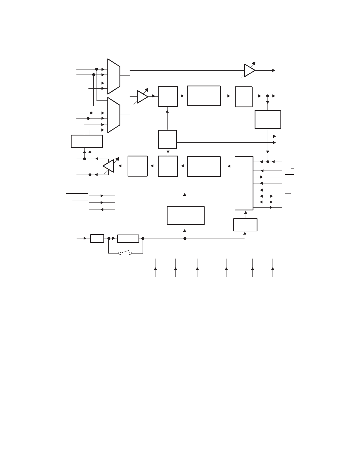
1.2 Functional Block Diagram
INP
INM
AUXP
AUXM
OUTP
OUTM
PWRDWN
RESET
MCLK
5
6
3
4
Analog
Loopback
23
24
16
15
28
FILT
18
÷N
MUX
MUX
PGA
Low
Pass
Filter
PLL (x4)
PGA
Sigma
-Delta
ADC
V
ref
Sigma
-Delta
DAC
Clock Circuit
Decimation
Interpolation
Internal
Filter
Filter
Buffer
Buffer
I/O
Control
PGA
Digital
Loopback
27
11
1
2
12
22
21
14
17
20
19
13
MONOUT
DOUT
REFP
REFM
DIN
M/S
FSD
ALTDATA
FC
FS
SCLK
FLAG
1–2
10 9 7 8
DV
SS
NOTE: Pin numbers shown are for the DW package.
DV
DD
AV
DD(PLL)AVSS(PLL)
26 25
AV
SS
AV
DD
Page 11
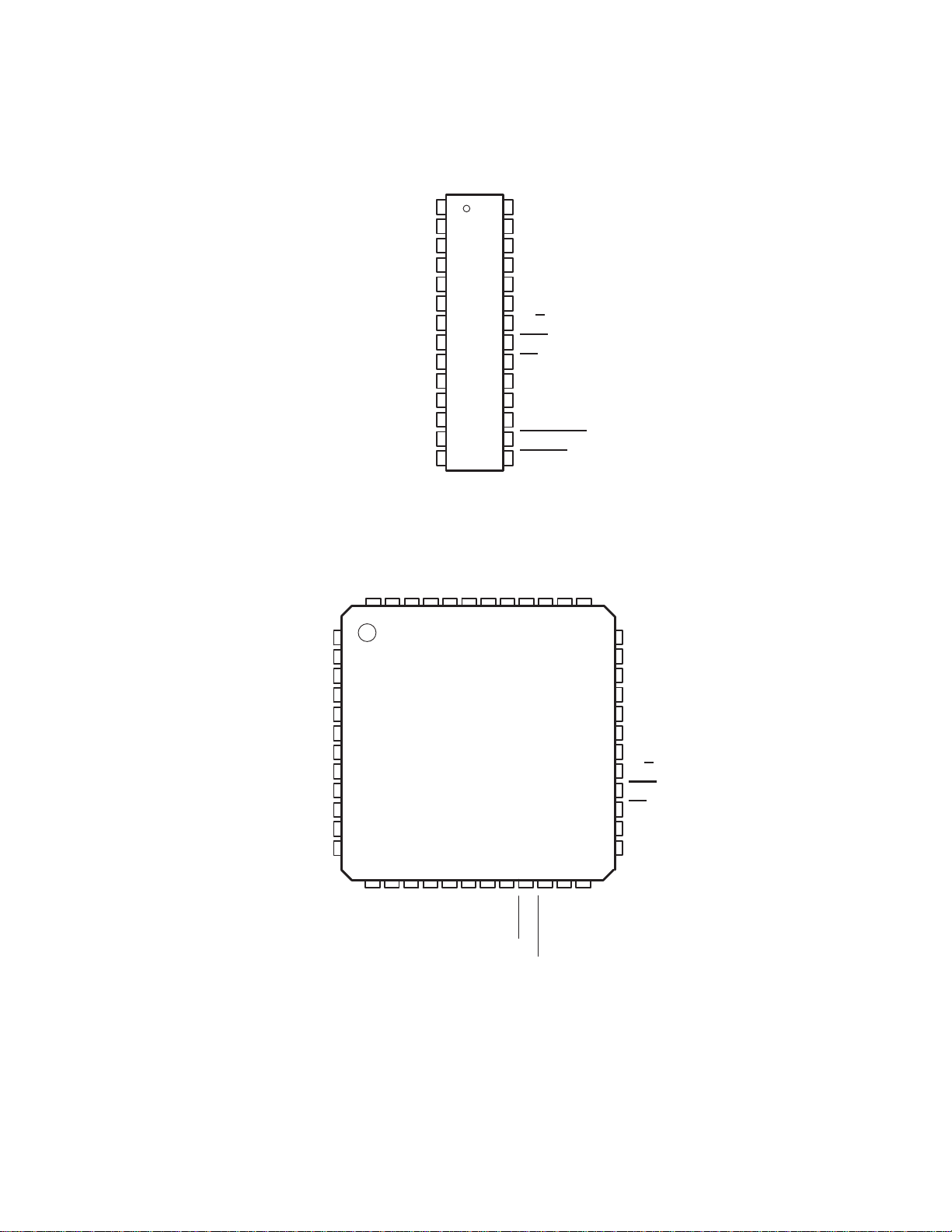
1.3 Terminal Assignments
REFP
REFM
AUXP
AUXM
INM
AV
DD(PLL)
AV
SS(PLL)
DV
DV
DOUT
FLAG
ALTDATA
AUXM
AUXP
DW PACKAGE
(TOP VIEW)
1
2
3
4
5
INP
6
7
8
9
DD
10
SS
11
12
DIN
13
14
PT PACKAGE
(TOP VIEW)
REFP
REFM
NC
FIL T
28
27
26
25
24
23
22
21
20
19
18
17
16
15
NC
FILT
MONOUT
AV
SS
AV
DD
OUTM
OUTP
M/S
FSD
FS
SCLK
MCLK
FC
PWRDWN
RESET
AV
NC
MONOUT
SS
NC
DD
AV
47 46 45 44 4348 42
1
INP
2
INM
3
NC
4
NC
NC
NC
NC
NC
DD
SS
5
6
7
8
9
10
11
12
13
14 15
AV
DD(PLL)
AV
SS(PLL)
DV
DV
NC
DOUT
NC – No internal connection
17 18 19 20
16
DIN
FLAG
NC
NC
40 39 3841
21
NC
37
22 23 24
FC
36
35
34
33
32
31
30
29
28
27
26
25
NC
OUTM
OUTP
NC
NC
NC
NC
NC
M/S
FSD
FS
SCLK
MCLK
RESET
AL TDATA
PWRDWN
1–3
Page 12
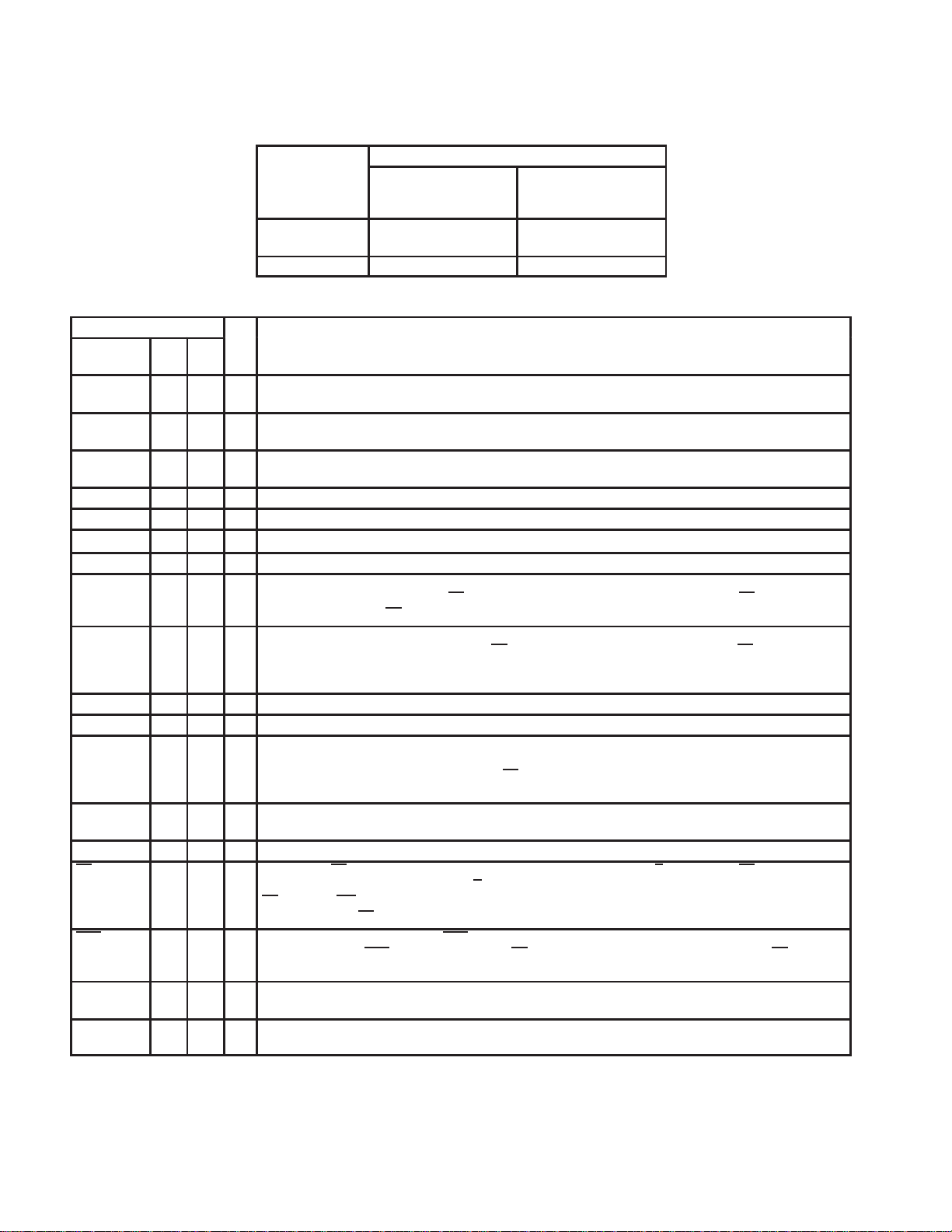
1.4 Ordering Information
PACKAGE
T
A
0°C to 70°C
–40°C to 85°C TLC320AD50IDW
SMALL OUTLINE
PLASTIC DIP
(DW)
TLC320AD50CDW
TLC320AD52CDW
QUAD FLAT PACK
(PT)
TLC320AD50CPT
TLC320AD52CPT
1.5 Terminal Functions
TERMINAL
NAME
ALTDATA 17 14 I Alternate data. ALTDATA signals are routed to DOUT during secondary communication if the phone mode
AUXM 48 4 I Inverting input to auxiliary analog input. AUXM requires an external single-pole antialias filter with a low output
AUXP 47 3 I Noninverting input to auxiliary analog input. AUXP requires an external single-pole antialias filter with a low
AV
DD
AV
DD(PLL)
AV
SS
AV
SS(PLL)
DIN 15 12 I Data input. DIN receives the DAC input data and register data from the external DSP (digital signal processor)
DOUT 14 11 O Data output. DOUT transmits the ADC output bits and register data, and is synchronized to SCLK. Data is
DV
DD
DV
SS
FC 23 17 I Hardware secondary communication request. When FC is set to high, a secondary communication, followed
FILT 43 28 O Bandgap filter. FILT is provided for decoupling of the bandgap reference, and provides 3.2 V. The optimal
FLAG 16 13 O Output flag. During phone mode, FLAG contains the value set in control 2 register.
FS 27 20 I/O Frame sync. FS is an output when the device is configured as a master (M/S pin tied high). FS is an input when
FSD 28 21 O Frame sync delayed output. The FSD (active-low) output synchronizes a slave device to the frame sync of
INM 2 6 I Inverting input to analog modulator. INM requires an external single-pole antialias filter with a low output
INP 1 5 I Noninverting input to analog modulator. INP requires an external single-pole antialias filter with a low output
NOTES: 1. Separate analog and digital power and ground pins are supplied on this device. For best operation and results, the PC board designer
NO.PTNO.
37 25 I Analog ADC power supply (5 V only) (see Note 1)
5 7 I Analog power supply for the internal PLL (5 V only) (see Note 1)
39 26 I Analog ground (see Note 1)
7 8 I Analog ground for the internal PLL (see Note 1)
11 9 I Digital power supply (5 V or 3 V) (see Note 1)
12 10 I Digital ground (see Note 1)
should utilize separate analog and digital power supplies as well as separate analog and digital ground planes.
2. All digital inputs and outputs are TTL compatible, unless otherwise noted (for DVDD = 5 V).
I/O DESCRIPTION
DW
is enabled using control 2 register.
impedance and should be tied to AVSS if not used.
output impedance and should be tied to A VSS if not used.
and is synchronized to SCLK and FS
high impedance when FS
sent out at the rising edge of SCLK when FS
When configured as a master, DOUT is active only during the appropriate time slot. DOUT is in high
impedance during the frame syncs for the slaves.
by the primary communication, will occur to transfer data between this device and the external controller. FC
is sampled and latched on the rising edge of FS
3 for details.
capacitor value is 0.1 µF (ceramic). This voltage node should be loaded only with a high-impedance dc load.
the device is configured as a slave (M/S
FS
goes low. FS is internally generated in the master mode for the master device and all slave devices. In
the master mode FS
the master device. FSD
is delayed in time by the number of shift clocks programmed in the control 3 register.
impedance.
impedance.
is not active.
is low during data transfer.
is applied to the slave FS input and is the same duration as the master FS signal but
. Data is latched at the falling edge of SCLK when FS is low. DIN is at
pin tied low). When configured as a slave, data will transfer when
is low. DOUT is at high impedance when FS is not activated.
at the end of the primary serial communication. See section
1–4
Page 13
1.5 Terminal Functions (Continued)
TERMINAL
NAME
M/S 29 22 I Master/slave select input. When M/S is high, the device is the master. When M/S is low, the device is a slave.
MCLK 25 18 I Master clock. MCLK derives the internal clocks of the sigma-delta analog interface circuit.
MONOUT 40 27 O Monitor output. MONOUT allows for monitoring of the analog input and is a high-impedance output. The gain
OUTM 36 24 O Inverting output of the DAC. The OUTM output can be loaded with 600 Ω. OUTM is functionally identical with
OUTP 35 23 O Noninverting output of the DAC. The OUTP output can be loaded with 600 Ω. OUTP can also be used alone
PWRDWN 22 16 I Power down. When PWRDWN is pulled low, the device goes into a power-down mode, the serial interface
REFM 46 2 O Voltage reference filter output. REFM is provided for low-pass filtering of the internal bandgap reference. The
REFP 45 1 O Voltage reference filter positive output. REFP is provided for low-pass filtering of the internal bandgap
RESET 21 15 I Reset. RESET initializes all of the internal registers to their default values. The serial port can be configured
SCLK 26 19 I/O Shift clock. The SCLK signal clocks serial data in through DIN and out through DOUT during the frame-sync
NOTES: 1. Separate analog and digital power and ground pins are supplied on this device. For best operation and results, the PC board designer
NO.PTNO.
should utilize separate analog and digital power supplies as well as separate analog and digital ground planes.
2. All digital inputs and outputs are TTL compatible, unless otherwise noted (for DVDD = 5 V).
I/O DESCRIPTION
DW
or mute is selected using control 1 register.
and complementary to OUTP. OUTM can also be used alone for single-ended operation.
for single-ended operation.
is disabled. However, all the register values are sustained and the device resumes full power operation without
reinitialization when PWRDWN
programmed register contents (see paragraph 2.2.2 for more information).
optimal ceramic capacitor value is 0.1 µF and should be connected between REFM and REFP. DC voltage
at REFM is 0 V.
reference. The optimal ceramic capacitor value is 0.1 µF and should be connected between REFP and REFM.
DC voltage at REFP is 3.2 V.
to the default state accordingly. See section 6 and paragraph 2.2.1 for more information.
interval. When configured as an output (M/S
signal frequency by 256. When configured as an input (M/S
synchronous with the master clock and frame sync.
is pulled high again. PWRDWN resets the counters only and preserves the
high), SCLK is generated internally by multiplying the frame-sync
low), SCLK is generated externally and must be
1–5
Page 14

1.6 Definitions and Terminology
ADC Channel The ADC channel refers to all signal processing circuits between the analog input and the digital
conversion results at DOUT.
Channel Delay The delay for the analog signal at the ADC input to appear on the digital output. The delay for
the digital value at the DAC input to appear on the analog output.
d
d The alpha character
(see Section 3.2) when discussing other data bit portions of the register.
Dxx Dxx is the bit position in the primary data word (xx is the bit number).
DSxx DSxx is the bit position in the secondary data word (xx is the bit number).
DAC Channel DAC channel refers to all signal processing circuits between the digital data word applied to DIN
and the differential output analog signal available at OUTP and OUTM.
represents valid programmed or default data in the control register format
Data Transfer
Interval
The time during which data is transferred from DOUT and to DIN. The interval is 16 shift clocks
and the data transfer is initiated by the falling edge of the frame-sync signal.
FIR Finite duration impulse response
f
s
Frame Sync and
Sampling Period
The sampling frequency
Frame sync and sampling period is the time between falling edges of successive primary
frame-sync signals. It is always equal to 256 SCLK.
Frame Sync Frame sync refers only to the falling edge of the signal that initiates the data transfer interval.
The primary frame sync starts the primary communications, and the secondary frame sync
starts the secondary communications.
Frame-Sync
Interval
Host A host is any processing system that interfaces to DIN, DOUT, SCLK, FS
The frame-sync interval is the time period occupied by 16 shift clocks. The frame-sync signal
goes high on the seventeenth rising edge of SCLK.
, and/or MCLK.
PGA Programmable gain amplifier
Primary
Communications
Primary communications refers to the digital data transfer interval. Since the device is
synchronous, the signal data words from the ADC channel and to the DAC channel occur
simultaneously.
Secondary
Communications
Secondary communications refers to the digital control and configuration data transfer interval
into DIN and the register read data cycle from DOUT. The data transfer interval occurs when
requested by hardware or software.
Signal Data This refers to the input signal and all of the converted representations through the ADC channel
and the signal through the DAC channel to the analog output. This is contrasted with the purely
digital software control data.
X The alpha character X represents a
1–6
don’t care
bit-position within the control register format.
Page 15

1.7 Register Functional Summary
There are seven control registers that are used as follows:
Register 0 The No-Op register. Addressing register 0 allows secondary communications requests without altering
any other register.
Register 1 Control register 1. The data in this register controls:
• Software reset
• Software power down
• Normal or auxiliary analog inputs enabling
• Normal or auxiliary analog inputs monitoring
• Selection of monitor amplifier output gain
• Selection of digital loopback
• Selection of16-bit or (15+1)-bit mode of DAC operation
Register 2 Control register 2. The data in this register:
• Contains the output value of FLAG
• Selects phone mode
• Contains the output flag indicating a decimator FIR filter overflow
• Selects either 16-bit mode or (15+1)-bit mode of ADC operation
• Enables analog loopback
Register 3 Control register 3. The data in this register:
• Sets the number of SCLK delays between FS
• Informs the master device of how many slaves are connected in the chain
and FSD
Register 4 Control register 4. The data in this register:
• Selects the amplifier gain for the input and output amplifiers
N
• Sets the sample rate by choosing the value of
MCLK/(512
• Selects the PLL. If the PLL is selected, the sampling rate is set to MCLK/(128
bypassed, the sampling rate can be set to MCLK/(512
Register 5 Reserved for factory test. Do not write to this register.
Register 6 Reserved for factory test. Do not write to this register.
N
)
from 1 to 8 where fs = MCLK/(128 N) or
N
). If the PLL is
N
).
1–7
Page 16

1–8
Page 17

2 Detailed Description
2.1 Device Functions
2.1.1 Operating Frequencies and Filter Control
The sampling frequency is controlled by control register 4. When the internal PLL is enabled (D7=0), the sampling
frequency is derived from the following equation:
fs+
Sampling (conversion) frequency
When the internal PLL is disabled (D7=1), the sampling frequency is derived from the following equation:
fs+
Sampling (conversion) frequency
If the sampling frequency is lower than 7 kHz, the sampling frequency is derived from the master clock (MCLK) using
equation 2. The internal PLL must be bypassed. The PLL input clock for sampling frequencies lower than 7 kHz is
outside the working range for the PLL input clock.
The frequency of SCLK is derived from sampling frequency (fs) instead of MCLK. The equation is as follows:
SCLK
The cutoff frequency of the filter can not be controlled by register programming. The filter response is shown in the
specification for an 8 kHz sample rate. This pass band scales linearly with the sample rate.
+
256 f
s
MCLK
+
128 N
MCLK
+
512 N
(1)
(2)
(3)
2.1.2 ADC Signal Channel
The input signal is amplified and applied to the ADC input. The ADC converts the signal into discrete output digital
words in 2s-complement data format, corresponding to the instantaneous analog-signal value at the sampling time.
These 16-bit (or 15-bit) digital words, representing sampled values of the analog input signal after the PGA, are
clocked out of the serial port (DOUT) at the positive edge of SCLK during the frame-sync interval, one bit for each
SCLK and one word for each primary communication interval (256 SCLKs). The 16-bit or (15 + 1)-bit ADC mode is
programmed into the device using control register 2. The default setting is the (15 + 1)-bit mode after power-up.
During secondary communication, the data previously programmed into the registers can be read out. This read
operation is accomplished by sending the appropriate register address (DS12 – DS8) with the read bit (DS13) set
to 1 in through DIN during present secondary communication. If a register read is not requested, all 16 bits are cleared
to 0 in the secondary communication. The timing sequence is shown in Figure 2–1 and Figure 2–2.
2–1
Page 18

SCLK
FS
1 2 15 16 17
16 SCLKs
DOUT
(16-Bit)
DOUT
(15+1-Bit)
NOTES: A. The 16-bit or (15 + 1)-bit mode is programmed via control register 2.
B. M/S
is used to indicate whether the 15-bit data comes from master device or slave device. (Master: M/S = 1, Slave M/S = 0)
C. The MSB (D15) is stable (the host can latch the data in at this time) at the falling edge of SCLK #1, the last bit (D0,M/S
at the falling edge of SCLK #16.
D15
MSB
D15
MSB
D14
D14
Figure 2–1. Timing Sequence of ADC Channel (Primary Communication Only)
16 SCLKs
FS
DOUT
(16-Bit)
16-Bit ADC Data
DOUT
(15 +1-Bit)
15-Bit ADC Data
+ M/S
128 SCLKs
M/S + Register Address +
M/S
M/S
256 SCLKs
D1
D1
LSB
16 SCLKs
Register Data/
+ Register Address +
All 0s (see Note A)
M/S + Register Data/
+ All 0 (see Note A)
D0
LSB
M/S
) is stable
PrimarySecondaryPrimary
NOTE A: M/S
bit (DS15) in the secondary communication is used to indicate whether the register data (address and content) comes from the
master device or the slave device if the read bit is set. During register read operations, bits DS7 – DS0 are the contents of the specified
register. In register write operations, bits DS7 – DS0 are all 0s.
Figure 2–2. Timing Sequence of ADC Channel (Primary and Secondary Communication)
2.1.3 DAC Signal Channel
DIN receives the 16-bit serial data word (2s complement) from the host during the primary communications interval.
These 16-bit digital words, representing the analog output signal before PGA, are clocked into the serial port (DIN)
at the falling edge of SCLK during the frame-sync interval, one bit for each SCLK and one word for each primary
communication interval (256 SCLKs). The data are converted to a pulse train by the sigma-delta DAC, which consists
of a digital interpolation filter and a digital modulator. The output of the modulator is then passed to an internal
low-pass filter to complete the analog signal reconstruction. Finally , the resulting analog signal is applied to the input
of a programmable-gain amplifier, which is capable of driving a 600-Ω load differentially at OUTP and OUTM. The
timing sequence is shown in Figure 2–3.
2–2
Page 19

SCLK
FS
1 2 15 16
16 SCLKs
17
DIN
(16-Bit)
DIN
(15+1-Bit)
NOTES: A. The 16-bit or (15 + 1)-bit mode is programmed via control register 1.
B. d0 = 0 means no secondary communication request (software secondary communication request control—paragraph 3.2)
D15
MSB
d15
MSB
D14
d14
D1
d1
LSB
D0
LSB
d0=0
see Note B
Figure 2–3. Timing Sequence of DAC Channel (Primary Communication Only)
During secondary communication, the digital control and configuration data (together with the register address), are
clocked in through DIN. These 16-bits of data are used either to initialize the register, or to read the register content
through DOUT . If a register initialization is not required, a no-operation word (DS15–DS8 are all set to 0) can be used.
If DS13 is set to 1, the content of the control register, specified by DS12–DS8, will be sent out through DOUT during
the same secondary communication (see section 2.1.5). The timing sequence is shown in Figure 2–4.
PrimarySecondaryPrimary
16 SCLKs
FS
DIN (16-Bit)
(see Note A)
16-Bit DAC Data
DIN
(15 +1-Bit)
15-Bit DAC
Data + D0=1
(see Note B)
128 SCLKs
NOTES: A. FC has to be set high for a secondary communication request when 16–bit DAC data format is used (paragraph 3.2).
B. D0 = 1 means secondary communication request (software secondary communication request control—paragraph 3.2).
16 SCLKs
Register Read/Write
Register Read/Write
256 SCLKs
Figure 2–4. Timing Sequence of DAC Channel (Primary and Secondary Communication)
2.1.4 Serial Interface
The digital serial interface consists of the shift clock (SCLK), the frame-sync signal (FS), the ADC-channel data output
(DOUT), and the DAC-channel data input (DIN). During the primary frame synchronization interval, SCLK clocks the
ADC channel results out through DOUT and clocks 16-bit/(15+1)-bit DAC data in through DIN.
During the secondary frame-sync interval, SCLK clocks the register read data out through DOUT if the read bit (DS13)
is set to 1 and transfers control and device parameter in through DIN. The timing sequence is shown in Figures 2–2
and 2–4.
2.1.5 Register Programming
All register programming occurs during secondary communications through DIN, and data is latched and valid on the
falling edge of SCLK during the frame-sync signal. If the default value for a particular register is desired, that register
2–3
Page 20

does not need to be addressed during the secondary communications interval. The no-op command (DS15–DS8 all
set to 0) addresses the pseudoregister (register 0), and no register programming takes place during the
communications.
In addition, each register can be read back through DOUT during secondary communications by setting the read bit
(DS13) to 1. When the register is in the read mode, no data can be written to the register during this cycle. DS13 must
be cleared to write to the register.
For example, if the contents of control register 1 is desired to be read out from DOUT, the following procedure must
be performed through DIN:
1. Request secondary communication by setting either D0 = 1 (software request) or FC = high (hardware
request) during the primary communication interval.
2. At the secondary communication interval (FS
read control register 1
0 0 1 0 0 0 0 1 x x x x x x x x
), send data in the following format in through DIN:
DS15 DS0
3. Then the following data will be read from DOUT, the last 8 bits of DOUT will contain the register 1 data.
read control register 1 data
M/S 0 1 0 0 0 0 1 d d d d d d d d
DS15 DS0
Figure 2–5 is a timing diagram of this procedure.
FS
DIN
DOUT
P
S
Register 1 Read
Low 8 Bits (DS0–DS7) are the
Content of Register 1
Figure 2–5. Register 1 Read Operation Timing Diagram
If control register 1 needs to be programmed, the following procedure must be performed through DIN:
1. Request secondary communication by setting either D0 = 1 (software request) or FC = high (hardware
request) during the primary communication interval.
2. At the secondary communication interval (FS), send data in the following format in through DIN:
write control register 1 data
0 0 0 0 0 0 0 1 d d d d d d d d
DS15 DS0
3. Then the following data is generated from DOUT:
write control register 1
M/S 0 0 0 0 0 0 1 0 0 0 0 0 0 0 0
DS15 DS0
2–4
Page 21

Figure 2–6 is a timing diagram of this procedure.
FS
DIN
DOUT
P
S
Register Write
Low 8 Bits (DS0–DS7) are all 0
Figure 2–6. Register 1 Write Operation Timing Diagram
2.1.6 Sigma-Delta ADC
The sigma-delta analog-to-digital converter in the device is a sigma-delta modulator with 64-× oversampling. The
ADC provides high-resolution, low-noise performance using oversampling techniques. Due to the oversampling
employed, only single-pole antialiasing filters are required on the analog inputs.
2.1.7 Decimation Filter
The decimation filters reduce the digital data rate to the sampling rate. This is accomplished by decimating with a ratio
of 1:64. The output of the decimation filter is a 16-bit 2s-complement data word clocking at the sample rate selected
for that particular data channel. The bandwidth of the filter is 0.439 × f
and scales linearly with the sample rate.
sample
2.1.8 Sigma-Delta DAC
The sigma-delta digital-to-analog converter in the device is a sigma-delta modulator with 256-× oversampling. The
DAC provides high-resolution, low-noise performance using oversampling techniques.
2.1.9 Interpolation Filter
The interpolation filter resamples the digital data at a rate of 256 times the incoming sample rate. The high-speed
data output from the interpolation filter is then used in the sigma-delta DAC. The bandwidth of the filter is 0.439 ×
f
and scales linearly with the sample rate.
sample
2.1.10 Analog and Digital Loopback
The analog and digital loopbacks provide a means of testing the modem data ADC/DAC channels and can be used
for in-circuit system-level tests. The analog loopback routes the DAC low-pass filter output into the analog input where
it is then converted by the ADC into a digital word. The digital loopback, enabled by setting bit D1 in control 1 register
to 1, routes the ADC output to the DAC input on the device. Analog loopback is enabled by setting bit D3 in control
2 register to 1 (see section 6).
2.1.11 FIR Overflow Flag
The decimator FIR filter sets an overflow flag (bit D5) of control 2 register to indicate that the input analog signal has
exceeded the range of the internal decimation filter calculations. Once the FIR overflow flag has been set in the
register, it remains set until the register is read by the user. Reading this value resets the overflow flag.
If FIR overflow occurs, the input signal must be attenuated either by the PGA or some other method.
2–5
Page 22

2.2 Reset and Power-Down Functions
2.2.1 Software and Hardware Reset
The TLC320AD50C and TLC320AD52C reset the internal counters and registers in response to either of two events:
1. A low-going reset pulse is applied to terminal RESET
.
2. A 1 is written to the programmable software reset bit (D7 of control register 1).
Either event resets the control registers and clears all the sequential circuits in the device. Reset signals should be
at least 6 master clock periods long.
After hardware reset, the default contents of all registers is 0.
After a hardware or software reset, the AD50 and AD52 require a finite amount of time for the internal PLL to stabilize.
During this time, no control words or D/A data should be written to the device.
The reset sequence should be as follows:
1. Assert reset (pulse width encompassing at least 6 MCLK periods)
2. Deactivate reset
3. Wait for SCLKS to be generated by the master device. This will take approximately 100 µs.
4. Wait for 18 frame syncs to occur
5. Write control and configuration data
6. Collect conversion data
2.2.2 Software and Hardware Power Down
Except for the digital interface, most of the device enters the power-down mode when D6 in control 1 register is set
to 1. When PWRDWN is taken low, the entire device is powered down. In either case, the register contents are
preserved and the output of the monitor amplifier is held at the midpoint voltage to minimize pops and clicks.
The amount of power drawn during software power down is higher than it is during a hardware power down because
of the current required to keep the digital interface active. Additional differences between software and hardware
power-down modes are detailed in the following paragraphs. Figure 2–7 represents the internal power-down logic.
PWRDWN
Software Power Down
(Control Register 1, D6)
Internal TLC320AD50C
D6 is Programmed
Through a Secondary
Write Operation
Figure 2–7. Internal Power-Down Logic
2.2.2.1 Software Power Down
When D6 of control 1 register is set to 1, the device enters the software power-down mode. In this state, the digital
interface circuit is still active while the internal ADC and DAC channels and differential outputs OUTP and OUTM are
disabled, and DOUT and FSD are inactive. Register data in the secondary serial communications is still accepted,
but data in the primary serial communications is ignored. The device returns to normal operation when D6 of control
1 register is reset to 0.
2–6
Page 23

2.2.2.2 Hardware Power Down
When PWRDWN is held low, the device enters the hardware power-down mode. In this state, the internal clock control
circuit and the differential outputs OUTP and OUTM are disabled. All other digital I/Os either are disabled or remain
in the state they were in immediately before power down. DIN cannot accept any data input. The device can only be
returned to normal operation by taking and holding PWRDWN high. When not holding the device in the hardware
power-down mode, PWRDWN
should be tied high.
2.3 Master Clock Circuit
MCLK is the external master clock input. The internal clock circuit generates and distributes necessary clocks
throughout the device. An internal PLL circuit is used for upsampling to provide the appropriate clocks for the digital
filters and modulators.
When the device is in the master mode, SCLK and FS are derived from MCLK in order to provide clocking of the serial
communications between the device and its controller. When in the slave mode, SCLK and FS are both inputs.
2.4 Data Out (DOUT)
DOUT is placed in the high-impedance state on the rising edge of the frame sync. In the primary communication, the
data word is the ADC conversion result. In the secondary communication, the data is the register-read results when
requested by the read/write (R/W) bit. If a register read is not requested, the low eight bits of the secondary word are
all zeroes. The state of the master/slave (M/S) terminal is reflected by the MSB in secondary communication (DOUT ,
bit DS15) and the LSB in the primary communication (DOUT , bit D0) while in 15 + 1 mode. When the device is in the
slave mode, DOUT remains in a high-impedance state until a nonzero value is written as a number of slaves in control
register 3 (bits D7 and D6).
2.4.1 Data Out, Master Mode
In the master mode, DOUT is taken from the high-impedance state by the falling edge of the frame sync (FS) that
is assigned to DOUT. The most significant data bit then appears first on DOUT.
2.4.2 Data Out, Slave Mode
In the slave mode, DOUT is taken from the high-impedance state by the falling edge of the input frame sync (FS).
The most significant data bit then appears on DOUT . When in the slave mode, DOUT is not enabled until the control
3 register is programmed with the number of slaves. This must be done even if there is only one slave device.
2.5 Data In (DIN)
In a primary communication, the data word is the input digital signal to the DAC channel. If the (15+1)-bit data format
is used, the LSB (D0) is used to request a secondary communication. In a secondary communication, the data is the
control and configuration data that sets the device for a particular function (see Section 3, Secondary Serial
Communication for details).
2.6 FC (Hardware Secondary Communication Request)
The FC input provides for hardware requests for secondary communications. FC works in conjunction with the LSB
of the primary data word. The signal on FC is latched on the rising edge of the primary frame sync (FS). FC should
be tied low if not used.
2.7 Frame-Sync Function for TLC320AD50C
The frame-sync signal (FS) indicates the device is ready to send and receive data. The data transfer out of DOUT
and into DIN begins on the falling edge of the frame-sync signal.
2–7
Page 24

2.7.1 Frame Sync (FS) Function, Master Mode
The frame sync is generated internally and goes low on the rising edge of SCLK and remains low during a 16-bit data
transfer. In addition to generating its own frame-sync signal, the master also outputs a frame sync for each slave that
is being used (see Figures 2–8 and 2–9).
SCLK
PrimarySecondaryPrimary
16 SCLKs
16 SCLKs
(see Note A)
(see Note B)
NOTES: A. Primary and secondary serial communication
FS
FS
DIN/DOUT
B. Primary serial communication, only
PrimaryPrimary
128 SCLKs
256 SCLKs
Figure 2–8. Master Device Frame-Sync Signal With Primary and Secondary Communications
(No Slaves)
SCLK
(see Note A)
(see Note B)
Delay is m Shift Clocks
Legend:
MP:Master Primary (master device data is transferred in this period, DOUT of the slave device is in high impedance state).
SP: Slave Primary (slave device data is transferred in this period, DOUT of master device is in high impedance state).
MS:Master Secondary (master device control register information is transferred in this period, DOUT of the slave device is in high impedance state).
SS: Slave Secondary(slave device control register information is transferred in this period, DOUT of the master device is in high impedance state).
NOTES: A. Primary and secondary serial communications
B. Primary serial communication only
C.
FS
FS
(see Note C)
m
is the value programmed into the FSD register (control register 3: D0–D5)
MP
MP
SP MS
SP
128 SCLKs
SS MP
MP
256 SCLKs
Figure 2–9. Master Device Frame-Sync Signal With Primary and Secondary Communications
(With 1 Slave Device)
2.7.2 Frame Sync (FS) Function,Slave Mode
Frame-sync timing is generated externally by the master FSD (or the previous slave in a multislave configuration)
and is applied to FS
2–8
of the slave to control the ADC and DAC timing.
Page 25

2.7.3 Frame-Sync Delayed (FSD) Function, Master Mode
The timing relationships are as follows:
• When the FSD register (control 3 register) data is 0 (default state at power up), then FSD goes low 1/4 SCLK
prior to the rising edge of SCLK when FS goes low (Figure 2–10).
• When the FSD register data is greater than 17, then FSD goes low on the rising edge of SCLK that is the
FSD
register number of SCLKs after the falling edge of FS (Figure 2–11).
Register data values from 1 to 17 result in a default register value of zero and should not be used.
SCLK
MP and SP
FS
(P and S)
See Note B
FSD
(P and S)
See Note B
FS (P)
See Note B
FSD (P)
See Note B
NOTES: A. The DIN of master and slave devices share the same DIN bus during first initialization. The DOUT is occupied by the master device
only until the control 3 register of master and slave device is programmed with slave devices number and number of SCLKs between
FS and FSD (m>17).
B. P&S: Primary and secondary communications P: Primary communication only
See Note A
MS and SS
See Note A
Figure 2–10. Master Device FS and FSD Output When FSD Register (D0–D5, Control 3 Register) is 0
MP SP MS SS MP
FS
FSD
Delay is
SCLKs (m > 17)
NOTES: A. Since master and slave share the same DIN bus during first initialization, they share the same input data word. Only one write cycle
is needed to program control 3 register of master device and slave device(s).
B. After the control 3 register is programmed, the DIN or DOUT bus of master and slave(s) are separated by time, although they still
physically connect to each other.
m
128 SCLKs
256 SCLKs
Figure 2–11. Master Device FS and FSD Output After Control 3 Register Is Programmed
(One Slave Device)
2.7.4 Frame-Sync Delayed (FSD), Slave Mode
The master FSD is output to the first slave device and the first slave FSD is output to the second slave device and
so on (see Figure 2–12). The FSD
FSD timing sequence in the slave mode is as follows:
• When the FSD register data is 0, then FSD goes low 1/4 SCLK cycle before FS goes low.
• When the FSD register data is greater than 17, then FSD goes low on the rising edge of the SCLK that is
equal to the FSD register number of SCLKs after the falling edge of FS
output of each device is input to the FS terminal of the succeeding device. The
(see Figure 2–13).
2–9
Page 26
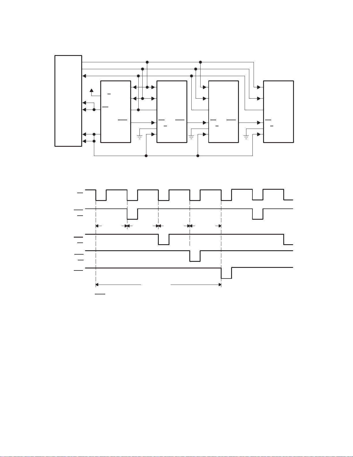
Data values from 1 to 17 should not be used.
CLKOUT
DX
DR
DV
DD
FSX
FSR FS
M/S
MCLK
DIN
DOUT
MCLK
DIN
DOUT
MCLK
DIN
DOUT
MCLK
DIN
DOUT
CLKX
CLKR
TMS320C5X
TMS320C2X
TMS320C54X
Master FS
Master FSD
Slave 1 FS
Slave 1 FSD
Slave 2 FS
Slave 2 FSD
Slave 3 FS
Slave 3 FSD
(see Note A)
FSD
SCLK
Master
FSD
FS
M/S M/S M/S
SCLK
Slave 1 Slave 2
FS
SCLK
FSD
Figure 2–12. Master With Slaves (To DSP Interface)
PP P P S
MS1S2S3M
Delay 1 Delay 2 Delay 3 Delay 4
128 SCLKs
S
S1
FS
SCLK
Slave 3
S
NOTE A: Slave 3 FSD
cannot be used.
Figure 2–13. Master-Slave Frame-Sync Timing After A Delay Has Been Programmed Into The FSD
Register (D0–D5 of Control 3 Register)
2–10
Page 27

2.8 Frame-Sync Function for TLC320AD52C
The frame-sync function for TLC320AD52C is very similar to that of the TLC320AD50C except the following:
1. TLC320AD52C can support only one slave.
2. The FSD terminal function can be disabled for TLC320AD52C by programming bit D2 in control 2 register.
3. The FSD value loaded into control 3 register must be multiplied by 2 to obtain the actual number of SCLKs
for the delay.
For example, if FSD register (control register 3) is programmed with 49H, it means that the TLC320AD52C has one
slave and the FSD terminal has 18 SCLKs delay after master primary FS output. See Figure 2–14.
MP SP MS SS MP
FS
FSD
Delay is ≥18
SCLKs
(See Note A)
NOTE A: Minimum SCLK delay number in FSD register is 9. This means that a delay of at least 18 SCLKs is required for proper operation of the
TLC320AD52C.
Figure 2–14. Master Device FS and FSD Output After Control 3 Register
128 SCLKs
256 SCLKs
Is Programmed With 49H
2.9 Multiplexed Analog Input and Output
The two differential analog inputs (INP and INM or AUXP and AUXM) are multiplexed into the sigma-delta modulator .
The performance of the AUX channel is similar to the normal input channel. A single-pole antialias filter must be
connected to INP and INM (also AUXP and AUXM, if used). If an RC is used for the single-pole filter (Figure 2–15)
the value of R should not be greater that 1 kΩ. The gain of the input amplifiers is set through the control register 4.
R
IN +
C
R
IN –
C
NOTES: A. The bandwidth of this RC antialias is determined by: (f0 = 1/(2π RC))
B. AUXP and AUXM need to be connected to AVSS if not used.
C. Bandwidth of the antialias filter can be 4
D. The input signal must have AVDD/2 dc or it must be ac-coupled.
× f
.
s
Figure 2–15. RC Antialias Filter
To produce the best possible common-mode rejection of unwanted signal performance, the analog signal is
processed differentially until it is converted to digital data. The signal applied to the terminals INM and INP should
be differential to preserve the device specifications. As much as 6 dB of signal level will be lost if the single-ended
input is used directly. The signal source driving the analog inputs (INP and INM or AUXP and AUXM) should have
a low source impedance for best low-noise performance and accuracy.
To obtain maximum dynamic range, the signal should be ac-coupled to the input terminal. The analog input signal
is self-biased to the midsupply voltage if the monitor-amplifier input source is selected as the same source for the
INP
INM
2–11
Page 28

ADC input. These input sources are selected by bits D4 and D5 of control register 1. The default condition self-biases
the input since the register default value selects INP and INM as the source for both the ADC and monitor amplifier
input (see Figure 2–16). A simple single-pole antialias filter with low output impedance must be connected to INP and
INM (also AUXP and AUXM, if used).
V
V
INP
INM
INP
35 kΩ
2.5 V
35 kΩ
INM
Figure 2–16. INP and INM Internal Self-Biased (2.5 V) Circuit
2.9.1 Analog Output
The OUTP and OUTM are differential outputs and can drive a typical 600-Ω load directly . Figure 2–17 shows the circuit
when load is ground referenced.
10 kΩ
5 V
OUTM
OUTP
10 kΩ
10 kΩ
10 kΩ
+
_
–5 V
TLE2062
Load
Figure 2–17. Differential Output Drive (Ground Referenced)
OUTP (Solid Line)
4 V
(Virtual 0)
2.5 V
1 V
OUTM (Dashed Line)
Digital Input Code Analog Output Voltage
(+FS) 0111 1111 1111 1111
(Virtual 0) 0000 0000 0000 0000
(–FS) 1000 0000 0000 0000
OUT +
4 V
2.5 V
1 V
OUT –
1 V
2.5 V
4 V
Figure 2–18. Digital Input Code vs Analog Output Voltage
2–12
Page 29

3 Serial Communications
DOUT, DIN, SCLK, FS, and FC are the serial communication signals. The digital output data from the ADC is taken
from DOUT . The digital input data for the DAC is applied to DIN. The synchronizing clock for the serial communication
data and the frame sync is taken from SCLK. The frame-sync pulse that encloses the ADC and DAC data transfer
interval is taken from FS
used. To read or write words that control both the options and the circuit configurations of the device, secondary
communication is used.
The purpose of the primary and secondary communications is to allow conversion data and control data to be
transferred across the same serial port. A primary transfer is always dedicated to conversion data. A secondary
transfer is used to set up and/or read the register values. A primary transfer occurs for every conversion period. A
secondary transfer occurs only when requested. Secondary serial communication can be requested either by
hardware (FC terminal) or by software (D0 of primary data input to DIN).
3.1 Primary Serial Communication
Primary serial communication is used both to transmit and receive conversion signal data. The DAC word length
depends on the state of bit D0 in control 1 register. After power up or reset, the device defaults to the 15-bit mode.
When the DAC word length is 15 bits, the last bit of the primary 16-bit serial communication word is a control bit used
to request secondary serial communication. In the 16-bit mode, all 16 bits of the primary communication word are
used as data for the DAC and the hardware terminal FC must be used to request secondary communication.
. For signal data transmitted from the ADC or to the DAC, primary serial communication is
Figure 3–1 shows the timing relationship for SCLK, FS
, DOUT, and DIN in a primary communication. The timing
sequence for this operation is as follows:
1. FS is brought low by the TLC320AD50C, TLC320AD50I, or TLC320AD52C.
2. A 16-bit word is transmitted from the ADC (DOUT) and a 16-bit word is received from the DAC (DIN).
3. FS
is brought high by the TLC320AD50C, TLC320AD50I, or TLC320AD52C, signaling the end of the data
transfer.
SCLK
FS
DIN
DOUT
NOTE: DIN is latched at the falling edge of SCLK. DOUT is sent out at the rising edge of SCLK
D15 D14 D13 D12 D11 D10 D5 D4 D3 D2 D1 D0
D15 D14 D13 D12 D11 D10 D5 D4 D3 D2 D1 D0
Figure 3–1. Primary Serial Communication Timing
3–1
Page 30

3.2 Secondary Serial Communication
Secondary serial communication is used to read or write 16-bit words that program both the options and the circuit
configurations of the device. Register programming always occurs during secondary communication. Four primary
and secondary communication cycles are required to program the four registers. If the default value for a particular
register is desired, then the register addressing can be omitted during secondary communications. The NOOP
command addresses a pseudoregister, register 0, and no register programming takes place during this secondary
communication. If secondary communication is desired for any device (either master or slave), then a secondary
communication must be requested for all devices, starting with the master. This results in a secondary frame sync
(FS
) for all devices. The NOOP command can be used for devices that do not need a secondary operation.
During secondary communication, a register may be written to or read from. When writing a value to a register, DIN
contains the value to be written. When reading the value in a register, the data is stepped out on DOUT.
There are two methods for initiating secondary communications:
1. By asserting a high level on FC
2. By asserting the LSB of the DIN 16-bit serial communication high while in the15-bit mode
Both methods are illustrated in Figure 3–2.
(Hardware)
FC
(LSB of DIN)
16-Bit Mode
(Control 1 Register, Bit 0)
Internal TLC320AD50C
Secondary
Request
Figure 3–2. Hardware and Software Methods to Make a Secondary Request
FC should be pulled high before the rising edge of the frame sync (FS). This causes the start of the secondary
communication, 128 SCLKs after the start of the primary communication frame. If slaves are present, FC should
remain high until the rising edge of the frame sync for the last slave.
The second method for secondary communication is by asserting the LSB high. The least significant bit (D0) can be
used for the secondary requests as shown in T able 3–1. The request is made by placing the device in the 15-bit DAC
mode and making the LSB of DIN equal to 1. All devices should be in the 15-bit DAC mode and secondary
communication should be requested for all devices.
Table 3–1. Least Significant Bit Control Function
CONTROL BIT D0 CONTROL BIT FUNCTION
0 No operation (NOOP)
1 Secondary communication request
If a secondary communication request is made, FS goes low after 128 SCLKs after the beginning of the primary frame.
3–2
Page 31

3.2.1 Hardware Secondary Serial Communication Request
The FC requests a secondary communication when it is asserted. The FC terminal is latched at the rising edge of
FS (primary communication), so FC should be pulled high before the rising edge of the primary frame sync (FS).
Figures 3–3 and 3–4 show the FS output from a master device.
FS
FC
DOUT
DIN
PPS
Secondary
Request
ADC Data Out
DAC Data In
Register
Read/Write
Register
Read/Write
No Secondary
Request
ADC Data Out
DAC Data In
Figure 3–3. FS Output When Hardware Secondary Serial Communication Is Requested Only Once
(No Slave)
PPPPSSSSP
FS
(Master)
FC
(See Note)
NOTE: FC of master device and slave devices should connect together.
S1 S2 S3MS1S2S3MM
Figure 3–4. FS Output When Hardware Secondary Serial Communication Is Requested Only Once
(Three Slaves)
3.2.2 Software Secondary Serial Communication Request
The LSB of the DAC data within a primary transfer can request a secondary communication when the device is in
the 15-bit mode.
For all serial communications, the most significant bit is transferred first. For a 16-bit ADC word and a 16-bit DAC word,
D15 is the most significant bit and D0 is the least significant bit. For a 15-bit DAC data word in a primary
communication, D15 is the most significant bit and D1 is the least significant bit. Bit D0 is then used for the secondary
communication request control. All digital data values are in 2s complement data format (Figure 3–5).
If the data format is set to the 16-bit word mode, all 16 bits are either ADC or DAC data and secondary communication
can then be requested only by hardware (FC terminal).
FS
DIN
Secondary Communication Request No Secondary Communication Request
NOTE: See Figure 3–8 for secondary communication DIN data format.
Figure 3–5. FS Output During Software Secondary Serial Communication Request (No Slave)
PSP
Data (D0 = 1)
Register
Read/Write
Data (D0 = 0)
3–3
Page 32

3.3 Conversion Rate Versus Serial Port
The SCLK frequency is set equal to the frequency of the frame-sync signal (FS) multiplied by 256. The conversion
rate or sample rate is equal to the frequency of FS.
3.4 Phone Mode Control
Phone mode control is provided for applications that need hardware control and monitoring of external events. By
allowing the device to drive the FLAG terminal (set through control 2 register), the host DSP is capable of system
control through the same serial port that connects the device. Along with this control is the capability of monitoring
the value of the ALTDATA terminal during a secondary communication cycle. One application for this function is in
monitoring RING DETECT or OFFHOOK DETECT from a phone answering system. FLAG allows response to these
incoming control signals. Figure 3–6 shows the timing associated with this operating mode.
PS
FS
Register Data
(8-Bits)
DOUT
(see Note A)
8-Bits
DOUT
(see Note B)
ALTDATA
NOTES: A. When DIN performs a read operation (set D13 to 1) during secondary communication.
B. When DIN perform a write operation (set D13 to 0) during secondary communication.
16-Bits
Figure 3–6. Phone Mode Timing When Phone Mode Is Enabled
3.5 DIN and DOUT Data Format
3.5.1 Primary Serial Communication DIN and DOUT Data Format (Figure 3–7)
(15+1) Bit Mode
DIN
DOUT
(15+1) Bit Mode
DIN
16-Bit Mode
D15 – D1
A/D and D/A Data
D15 – D1
D15 – D0
D0
Secondary
Communication Request
D0
M/S Bit
3–4
A/D and D/A Data
DOUT
16-Bit Mode
D15 – D0
Figure 3–7. Primary Communication DIN and DOUT Data Format
Page 33

3.5.2 Secondary Serial Communication DIN and DOUT Data Format (Figure 3–8)
Don’t Care
DS13=1
DIN (Read)
DS15 DS14 DS13 DS12 DS11 DS10 DS9 DS8
DS7 – DS0
DIN (Write)
DOUT (Read)
(Phone Mode Disabled)
DOUT (Write)
(Phone Mode Disabled)
DOUT (Read)
(Phone Mode Enabled)
DOUT (Write)
(Phone Mode Enabled)
Figure 3–8. Second Communication DIN and DOUT Data Format
R/W
DS15 DS14 DS13 DS12 DS11 DS10 DS9 DS8
DS13=0
DS13=1
DS15 DS14 DS13 DS12 DS11 DS10 DS9 DS8
M/S
DS15 DS14 DS13 DS12 DS11 DS10 DS9 DS8
DS13=0
DS15 – DS8: ALTDATA
Register Address
Register Address
DS15 – DS0: ALTDATA
Data to the
Register
DS7 – DS0
Register Data
DS7 – DS0
All 0
DS7 – DS0
DS7 – DS0: Register Data
3–5
Page 34

3–6
Page 35

4 Specifications
4.1 Absolute Maximum Ratings Over Operating Free-Air Temperature Range
(Unless Otherwise Noted)
Supply voltage range, DV
Output voltage range, DOUT, FS, SCLK, FLAG –0.3 V to DVDD + 0.3 V. . . . . . . . . . . . . . . . . . . . . . . . . . . . . .
Output voltage range, OUTP, OUTM –0.3 V to VDD + 0.3 V. . . . . . . . . . . . . . . . . . . . . . . . . . . . . . . . . . . . . . . . . .
Input voltage range, DIN, PWRDWN, RESET, ALTDATA, MCLK, FC –0.3 V to DVDD + 0.3 V. . . . . . . . . . . .
Input voltage range, INP, INM, AUXP, AUXM –0.3 V to V
Case temperature for 10 seconds: DW package 260°C. . . . . . . . . . . . . . . . . . . . . . . . . . . . . . . . . . . . . . . . . . . . .
Operating free-air temperature range, TLC320AD50C/52C, TA 0°C to 70°C. . . . . . . . . . . . . . . . . . . . . . . . . . . .
Operating free-air temperature range, TLC320AD50I, TA –40°C to 85°C. . . . . . . . . . . . . . . . . . . . . . . . . . . . . .
Storage temperature range, T
†
Stresses beyond those listed under “absolute maximum ratings” may cause permanent damage to the device. These are stress ratings only, and
functional operation of the device at these or any other conditions beyond those indicated under “recommended operating conditions” is not
implied. Exposure to absolute-maximum-rated conditions for extended periods may affect device reliability.
NOTE 1: All voltage values are with respect to VSS.
DD,
†
AVDD (see Note 1) –0.3 V to 7 V. . . . . . . . . . . . . . . . . . . . . . . . . . . . . . . . . . . . . . .
–65°C to 150°C. . . . . . . . . . . . . . . . . . . . . . . . . . . . . . . . . . . . . . . . . . . . . . . . . .
stg
DD
+ 0.3 V. . . . . . . . . . . . . . . . . . . . . . . . . . . . . . . . . .
4.2 Recommended Operating Conditions
MIN NOM MAX UNIT
Supply voltage, AVDD (see Note 2) 4.75 5.5 V
Analog signal input voltage, V
Differential output load resistance, OUTP, OUTM, R
Differential output load capacitance, OUTP, OUTM, C
ADC or DAC conversion rate 8 22.05 kHz
Operating free-air temperature, T
NOTE 2: Voltages at analog inputs and outputs and AVDD are with respect to the AVSS terminal.
I(analog)
A
Differential (INP–INM) peak, for full scale operation 6 V
L
L
600 Ω
15 pF
0 70 °C
4.2.1 Recommended Operating Conditions, DVDD = 5 V
MIN NOM MAX UNIT
Supply voltage, DVDD (see Note 3) 4.5 5.5 V
High-level input voltage, V
Low-level input voltage, V
MCLK frequency 8.192 11.290 MHz
NOTE 3: Voltages at digital inputs and outputs and DVDD are with respect to the DVSS terminal.
IH
IL
2 V
0.8 V
4.2.2 Recommended Operating Conditions, DVDD = 3 V
MIN NOM MAX UNIT
Supply voltage, DVDD (see Note 3) 2.7 3 3.3 V
High-level input voltage, V
Low-level input voltage, V
MCLK frequency 8.192 11.290 MHz
NOTE 3: Voltages at digital inputs and outputs and DVDD are with respect to the DVSS terminal.
IH
IL
1.8 V
0.6 V
4–1
Page 36

4.3 Electrical Characteristics Over Recommended Operating Free-Air Temperature
Filter gain relative to gain at 1020 H
dB
PARAMETER
TEST CONDITIONS
UNIT
Range, DV
4.3.1 Digital Inputs and Outputs, MCLK = 8.192 MHz, fs = 8 kHz, DVDD = 5 V
V
High-level output voltage, DOUT IO = 360 µA 4 5 V
OH
V
Low-level output voltage, DOUT IO = –2 mA 0.2 0.4 V
OL
I
High-level input current, any digital input VIH = 5 V 10 µA
IH
I
Low-level input current, any digital input VIL = 0.8 V 10 µA
IL
C
Input capacitance 5 pF
i
C
Output capacitance 5 pF
o
4.3.2 Digital Inputs and Outputs, MCLK = 8.192 MHz, fs = 8 kHz, DVDD = 3 V
V
High-level output voltage, DOUT IO = 360 µA 2.4 3 V
OH
V
Low-level output voltage, DOUT IO = –2 mA 0.2 0.4 V
OL
I
High-level input current, any digital input VIH = 3 V 10 µA
IH
I
Low-level input current, any digital input VIL = 0.6 V 10 µA
IL
C
Input capacitance 5 pF
i
C
Output capacitance 5 pF
o
= 5 V, RL = 600 Ω (Unless Otherwise Noted)
DD
PARAMETER TEST CONDITIONS MIN TYP MAX UNIT
PARAMETER TEST CONDITIONS MIN TYP MAX UNIT
4.3.3 ADC Channel, MCLK = 8.192 MHz, fs = 8 kHz (see Note 4, Figures 5-6 and 5-7)
PARAMETER TEST CONDITIONS MIN TYP MAX UNIT
0 to 300 Hz –0.5 0.2
300 Hz to 3 kHz –0.25 0.25
z
NOTE 4: The filter gain outside of the passband is measured with respect to the gain at 1020 Hz. The analog input test signal is a sine wave with
0 dB = 4 VPP as the reference level for the analog input signal. The passband is 0 to 3600 Hz for an 8-kHz sample rate. This passband
scales linearly with the sample rate.
3.3 kHz –0.35 0.3
3.6 kHz –3
4 kHz –40
≥ 4.4 kHz –74
4.3.4 ADC Dynamic Performance, MCLK = 8.192 MHz, fs = 8 kHz
4.3.4.1 ADC Signal-to-Noise (see Note 5 and Figure 5-10)
TLC320AD50C/52C TLC320AD50I
MIN TYP MAX MIN TYP MAX
VI = –1 dB (5.35 V) 85 89 83 87
VI = –9 dB (2.13 V) 77 81 75 79
Signal-to-noise ratio (SNR)
NOTE 5: The test condition is a 1020-Hz input signal with an 8-kHz conversion rate. Input and output are referenced to AVDD/2.
VI = –40 dB (60 mV) 46 50 44 48
VI = –65 dB (3 mV) 21 25 19 23
V
= –9 dB 77 81 75 79
AUX
dB
4–2
Page 37

4.3.4.2 ADC Signal-to-Distortion (see Note 5 and Figure 5-11)
PARAMETER
TEST CONDITIONS
UNIT
PARAMETER
TEST CONDITIONS
UNIT
Filter gain relative to gain at 1020 H
dB
TLC320AD50C/52C TLC320AD50I
MIN TYP MAX MIN TYP MAX
VI = –3 dB (4.25 V) 80 85 79 84
VI = –9 dB (2.13 V) 79 90 78 89
Signal-to-total harmonic distortion (THD)
NOTE 5. The test condition is a 1020-Hz input signal with an 8-kHz conversion rate. Input and output are referenced to VDD/2.
VI = –40 dB (60 mV) 67 72 66 71
VI = –65 dB (3 mV) 43 48 42 47
V
= –9 dB 79 90 78 89
AUX
4.3.4.3 ADC Signal-to-Distortion + Noise (see Note 5 and Figure 5-12)
TLC320AD50C/52C TLC320AD50I
MIN TYP MAX MIN TYP MAX
VI = –3 dB (4.25 V) 78 82 76 80
VI = –9 dB (2.13 V) 76 80 74 78
Signal-to-total harmonic distortion + noise (THD + N)
NOTE 5. The test condition is a 1020-Hz input signal with an 8-kHz conversion rate. Input and output are referenced to VDD/2.
VI = –40 dB (60 mV) 45 49 43 47
VI = –65 dB (3 mV) 20 24 19 22
V
= –9 dB 76 80 74 78
AUX
4.3.5 ADC Channel Characteristics
dB
dB
PARAMETER TEST CONDITIONS MIN TYP MAX UNIT
V
I(PP)
E
G
E
O(ADC)
CMRR Common-mode rejection ratio at INM, INP or AUXM, AUXP VI = –1 dB at 1020 Hz 74 dB
R
i
Peak-to-peak input voltage
(differential (INP–INM) peak, for full scale operation)
Dynamic range VI = –1 dB (5.35 V) 88 dB
Interchannel isolation 100 dB
Gain error VI = –1 dB at 1020 Hz ± 0.3 dB
ADC converter offset error 5 15 mV
Idle channel noise (on-chip reference) V
Input resistance TA = 25°C 35 kΩ
Channel delay 17/f
INP, INM
= 2.5 V 75 µV rms
s
6 V
s
4.3.6 DAC Path Filter, MCLK = 8.192 MHz, fs = 8 kHz (see Note 6, Figures 5-8 and 5-9)
PARAMETER TEST CONDITIONS MIN TYP MAX UNIT
0 to 300 Hz –0.5 0.2
300 Hz to 3 kHz –0.25 0.25
z
NOTE 6: The filter gain outside of the pass band is measured with respect to the gain at 1020 Hz. The input signal is the digital equivalent of a
sine wave (digital full scale = 0 dB). The nominal differential DAC channel output with this input condition is 6 V
is 0 to 3600 Hz for an 8-kHz sample rate. This pass band scales linearly with the conversion rate.
3.3 kHz –0.35 0.3
3.6 kHz –3
4 kHz –40
≥ 4.4 kHz –74
. The pass band
I(PP)
4–3
Page 38

4.3.7 DAC Dynamic Performance
PARAMETER
TEST CONDITIONS
UNIT
Signal-to-noise ratio (SNR)
dB
Signal-to-noise ratio (SNR)
dB
PARAMETER
TEST CONDITIONS
UNIT
Signal-to-total harmonic distortion (THD)
dB
Signal-to-total harmonic distortion (THD)
dB
PARAMETER
TEST CONDITIONS
UNIT
Signal-to-total harmonic distortion
noise (THD
N)
dB
4.3.7.1 DAC Signal-to-Noise When Load is 600 Ω (see Note 7 and Figure 5-13)
TLC320AD50C/52C TLC320AD50I
MIN TYP MAX MIN TYP MAX
VI = 0 dB 85 89 83 87
VI = –9 dB 76 80 74 78
VI = –40 dB 45 49 43 47
VI = –65 dB 20 24 18 22
NOTE 7: The test condition is the digital equivalent of a 1020-Hz input signal with an 8-kHz conversion rate. The test is measured at output of
application schematic low-pass filter. The test is conducted in 16-bit mode.
4.3.7.2 DAC Signal-to-Noise When Load is 10 kΩ (see Note 7)
PARAMETER TEST CONDITIONS MIN TYP MAX UNIT
VI = 0 dB 89
VI = –9 dB 80
VI = –40 dB 50
VI = –65 dB 25
NOTE 7: The test condition is the digital equivalent of a 1020-Hz input signal with an 8-kHz conversion rate. The test is measured at output of
application schematic low-pass filter. The test is conducted in 16-bit mode.
4.3.7.3 DAC Signal-to-Distortion When Load is 600 Ω (see Note 7, Figure 5-14)
TLC320AD50C/52C TLC320AD50I
MIN TYP MAX MIN TYP MAX
VI = –3 dB 76 80 74 78
VI = –9 dB 84 90 82 88
VI = –40 dB 64 72 62 70
VI = –65 dB 42 48 40 46
NOTE 7: The test condition is the digital equivalent of a 1020-Hz input signal with an 8-kHz conversion rate. The test is measured at output of
application schematic low-pass filter. The test is conducted in 16-bit mode.
4.3.7.4 DAC Signal-to-Distortion When Load is 10 kΩ (see Note 7)
NOTE 7: The test condition is the digital equivalent of a 1020-Hz input signal with an 8-kHz conversion rate. The test is measured at output of
application schematic low-pass filter. The test is conducted in 16-bit mode.
4.3.7.5 DAC Signal-to-Distortion+Noise When Load is 600 Ω (see Note 7, Figure 5-15)
NOTE 7: The test condition is the digital equivalent of a 1020-Hz input signal with an 8-kHz conversion rate. The test is measured at output of
4–4
application schematic low-pass filter. The test is conducted in 16-bit mode.
PARAMETER TEST CONDITIONS MIN TYP MAX UNIT
VI = –3 dB 82
VI = –9 dB 91
VI = –40 dB 77
VI = –65 dB 49
TLC320AD50C/52C TLC320AD50I
MIN TYP MAX MIN TYP MAX
VI = –3 dB 75 79 72 76
+
+
VI = –9 dB 75 79 72 76
VI = –40 dB 45 49 42 46
VI = –65 dB 20 24 17 21
Page 39

4.3.8 DAC Channel Characteristics
I
(analog)
Power supply current, ADC
mA
I
(PLL)
Power supply current, PLL
mA
I
(digital 1)
Power supply current, digital
I
(digital 2)
Power supply current, digital, DV
3 V
PDPower dissi ation
mW
PARAMETER TEST CONDITIONS MIN TYP MAX UNIT
Dynamic range 88 dB
Interchannel isolation 100 dB
E
Gain error, 0 dB VO = 0 dB at 1020 Hz ±0.3 dB
G
Idle channel narrow band noise 0 – 4 kHz, See Note 8 125 µV rms
V
Output offset voltage at OUT (differential) DIN = All 0s 30 mV
OO
RL = 600 Ω typ (see Figure 2–17) with internal
V
Analog output voltage, OUTP–OUTM
O
Total out of band energy (0.55 fs to 3 MHz) –45 dB
Channel delay 18/f
NOTES: 8. The conversion rate is 8 kHz; the-out-of-band measurement is made from 4400 Hz to 3 MHz.
9. The digital input to the DAC channel at DIN is in 2s complement format. The TLC320AD50C/52C DAC is of the voltage-type and
requires a load resistor for current to voltage conversion.
reference and full-scale digital input,
See Note 9, differential
4.3.9 Power Supply, AVDD = DVDD = 5 V, No Load
PARAMETER TEST CONDITIONS MIN TYP MAX UNIT
DD
DD
DD
DD
pp
pp
pp
pp
=
DD
p
Operating 18 24
Power down 1
Operating 2 4
Power down 0.5
Operating 4 6 mA
Power down 10 µA
Operating 4 mA
Power down 10 µA
Operating 120 170
H/W-power down 7.5 20
6 V
PP
s
4.3.10 Power-Supply Rejection, AVDD = DVDD = 5 V (see Note 10)
PARAMETER TEST CONDITIONS MIN TYP MAX UNIT
AV
DV
DV
NOTE 10: Power supply rejection measurements are made with both the ADC and the DAC channels idle and a 200-mV peak-to-peak signal
Supply voltage rejection ratio, analog supply fi = 0 to fs/2 50
DD
Supply voltage rejection ratio, DAC channel fi = 0 to 30 kHz 40
DD
Supply voltage rejection ratio, ADC channel fi = 0 to 30 kHz 50
DD
applied to the appropriate supply .
dB
4.4 Timing Characteristics (see Parameter Measurement Information)
4.4.1 Master Mode Timing Requirements
MIN NOM MAX UNIT
t
d1
t
su1
t
h1
t
d(CH–FDL)
t
wH
t
wL
Delay time, SCLK↑ to FS↓ 0
Setup time, DIN, before SCLK low 25
Hold time, DIN, after SCLK low 20
Delay time, SCLK high to FSD low (see Figure 5–1) 50
Pulse duration, MCLK high 32
Pulse duration, MCLK low 20
ns
4–5
Page 40

4.4.2 Slave Mode Timing Requirements
t
d4
t
su2
t
h2
t
d(FL–FDL)
t
d(CH–FDL)
t
wH
t
wL
Delay time, SCLK↑ to FS↓ 0
Setup time, DIN, before SCLK low 20
Hold time, DIN, after SCLK low 20
Delay time, FS low to FSD low, (see Figure 5–2) 40
Delay time, SCLK high to FSD low, slave mode (see Figure 5–3) 50
Pulse duration, MCLK high 32
Pulse duration, MCLK low 20
4.4.3 Master Mode Switching Characteristics
PARAMETER TEST CONDITIONS MIN TYP MAX UNIT
t
t
t
Delay time, SCLK↑ to DOUT 20
d2
Enable time, FS↓ to DOUT
en1
Disable time, FS↑ to DOUT Hi-Z 20
dis1
4.4.4 Slave Mode Switching Characteristics
PARAMETER TEST CONDITIONS MIN TYP MAX UNIT
t
t
t
Delay time, SCLK↑ to DOUT 20
d5
Enable time, FS↓ to DOUT
en2
Disable time, FS↑ to DOUT Hi-Z 20
dis2
CL = 20 pF
CL = 20 pF
MIN NOM MAX UNIT
ns
25
ns
25
ns
4.4.5 Reset Timing
t
Reset pulsewidth 6 MCLKs
PW
4.4.6 Other
t
t
Setup time, FC before FS↑ 10
su3
Hold time, FC after FS↑ 10 ns
h3
PARAMETER MIN TYP MAX UNIT
ns
PARAMETER MIN TYP MAX UNIT
ns
4–6
Page 41

5 Parameter Measurement Information
0.8 V
2.4 V
0.8 V
SCLK Period/4
t
d(CH-FDL)
SCLK
FSD
FS
NOTE A: Timing shown is for the TLC320AD50C/52C operating as the master device. The programmed data value in the FSD register is 0. D0
through D5 of control 3 register are all 0.
Figure 5–1. Master FS and FSD Timing
FS
FSD
NOTE A: Timing shown is for the TLC320AD50C/52C operating in the slave mode (FS and SCLK signals are generated externally). The
programmed data value in the FSD register is 0.
0.8 V
0.8 V
t
d(FL-FDL)
Figure 5–2. Slave FS to FSD Timing
SCLK
FSD
NOTE A: Timing shown is for the TLC320AD50C/52C operating in the slave mode (FS
data value in the FSD register greater than 18 decimal. D0 through D5 of control 3 register are greater than 17.
0.8 V
0.8 V
t
d(CH-FDL)
Figure 5–3. Master/Slave SCLK to FSD Timing
and SCLK signals are generated externally). There is a
5–1
Page 42

MCLK
SCLK
FS
t
wH
t
wL
t
d1
t
d2
t
en1
DOUT
t
su1
DIN
NOTE A: The master mode and D0 through D5 of control 3 register are greater than 17.
D15 D14
D15 D14
t
h1
Figure 5–4. Serial Communication Timing (Master Mode)
t
wH
MCLK
t
wL
SCLK
t
FS
d4
t
en2
t
d5
t
dis1
t
dis2
5–2
DOUT
DIN
D15 D14
t
su2
D15 D14
t
h2
Figure 5–5. Serial Communication Timing (Slave Mode)
Page 43
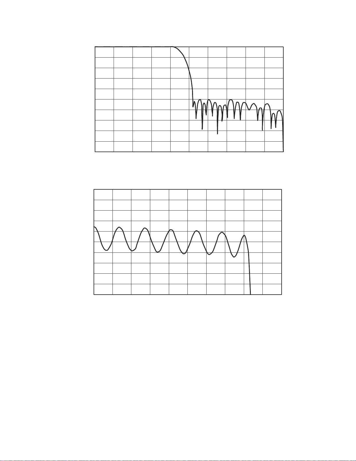
– 16
– 32
– 48
– 64
– 80
– 96
Attenuation – dB
– 112
– 128
– 144
0 0.8 1.6 2.4 3.2 4 4.8
fI – Input Frequency – kHz
5.6 6.4 7.2 8
Figure 5–6. ADC Channel Filter Response (MCLK = 8.192 MHz, fs = 8 kHz)
0.5
0.4
0.3
0.2
0.1
0
– 0.1
Attenuation – dB
– 0.2
– 0.3
– 0.4
– 0.5
0 0.4 0.8 1.2 1.6 2 2.4
fI – Input Frequency – kHz
2.8 3.2 3.6 4
Figure 5–7. ADC Channel Filter Passband Ripple (MCLK = 8.192 MHz, fs = 8 kHz)
5–3
Page 44

– 16
– 32
– 48
– 64
– 80
– 96
Attenuation – dB
– 112
– 128
– 144
0 0.8 1.6 2.4 3.2 4 4.8
fI – Input Frequency – kHz
5.6 6.4 7.2 8
Figure 5–8. DAC Channel Filter Response (MCLK = 8.192 MHz, fs = 8 kHz)
0.5
0.4
0.3
0.2
0.1
0
– 0.1
Attenuation – dB
– 0.2
– .03
– 0.4
– 0.5
0 0.4 0.8 1.2 1.6 2 2.4
fI – Input Frequency – kHz
2.8 3.2 3.6 4
Figure 5–9. DAC Channel Filter Passband Ripple (MCLK = 8.192 MHz, fs = 8 kHz)
5–4
Page 45

90
ADC SIGNAL-TO-NOISE RATIO
vs
INPUT SIGNAL
ADC SIGNAL-TO-DISTORTION RATIO
vs
INPUT SIGNAL
100
80
70
60
50
40
30
20
ADC – Signal-To-Noise Ratio – dB
10
0
–65 –40 –9 –3
8 kHz Conversion Rate
MCLK = 8.192 MHz
–2 –1 0
Input Signal – dB
Figure 5–10
ADC SIGNAL-TO-(NOISE AND DISTORTION) RATIO
vs
INPUT SIGNAL
90
80
90
80
70
60
50
40
30
20
ADC – Signal-To-Distortion Ratio – dB
10
0
–65 –40 –9 –3
DAC SIGNAL-TO-NOISE RATIO
90
80
8 kHz Conversion Rate
MCLK = 8.192 MHz
–2 –1 0
Input Signal – dB
Figure 5–11
vs
INPUT SIGNAL
70
60
50
40
30
20
8 kHz Conversion Rate
10
ADC – Signal-To-(Noise and Distortion) Ratio – dB
0
–65 –40 –9 –3
MCLK = 8.192 MHz
Input Signal – dB
Figure 5–12 Figure 5–13
–2 –1 0
70
60
50
40
30
20
DAC – Signal-To-Noise Ratio – dB
10
0
–65 –40 –9 –3
8 kHz Conversion Rate
MCLK = 8.192 MHz
–2 –1 0
Input Signal – dB
5–5
Page 46

100
90
80
70
60
50
40
30
DAC SIGNAL-TO-DISTORTION RATIO
vs
INPUT SIGNAL
20
DAC – Signal-To-Distortion Ratio – dB
10
0
–65 –40 –9 –3
8 kHz Conversion Rate
MCLK = 8.192 MHz
–2 –1 0
Input Signal – dB
Figure 5–14
DAC SIGNAL-TO-(NOISE AND DISTORTION) RATIO
vs
INPUT SIGNAL
90
80
70
60
50
40
30
20
8 kHz Conversion Rate
10
MCLK = 8.192 MHz
5–6
DAC – Signal-To-(Noise and Disrortion) Ratio – dB
0
–65 –40 –9 –3
Input Signal – dB
Figure 5–15
–2 –1 0
Page 47

6 Register Set
Bits D12 through D8 in a secondary serial communication comprise the address of the register that is written with
data carried in D7 through D0. D13 determines a read or write cycle to the addressed register. When low , a write cycle
is selected.
The following table shows the register map.
Table 6–1. Register Map
REGISTER NO. D15 D14 D13 D12 D11 D10 D9 D8 REGISTER NAME
0 0 0 0 0 0 0 0 0 No operation
1 0 0 0 0 0 0 0 1 Control 1
2 0 0 0 0 0 0 1 0 Control 2
3 0 0 0 0 0 0 1 1 Control 3
4 0 0 0 0 0 1 0 0 Control 4
6.1 Control Register 1
Table 6–2. Control Register 1
D7 D6 D5 D4 D3 D2 D1 D0 DESCRIPTION
1 – – – – – – – Software reset
0 – – – – – – – Software reset not asserted
– 1 – – – – – – Software power down (analog and filters)
– 0 – – – – – – Software power down (not asserted)
– – 1 – – – – – Select AUXP and AUXM for ADC
– – 0 – – – – – Select INP and INM for ADC
– – – 0 – – – – Select INP and INM for monitor
– – – 1 – – – – Select AUXP and AUXM for monitor
– – – – 1 1 – – Monitor amplifier gain = –18 dB (see Note 1)
– – – – 1 0 – – Monitor amplifier gain = –8 dB (see Note 1)
– – – – 0 1 – – Monitor amplifier gain = 0 dB (see Note 1)
– – – – 0 0 – – Monitor amp mute
– – – – – – 1 – Digital loopback asserted
– – – – – – 0 – Digital loopback not asserted
– – – – – – – 1 16-bit DAC mode (hardware secondary requests)
– – – – – – – 0 Not 16-bit DAC mode (software secondary requests) [(15+1)– bit mode]
Default value: 0 0 0 0 0 0 0 0
NOTE 1: These gains are for a single-ended input. The gain is 6 dB lower with a differential input.
A software reset is a one-shot operation and this bit is cleared to 0 after reset. It is not necessary to write a 0 to end
the master reset operation. Writing 0s to the reserved bits is suggested.
6–1
Page 48

6.2 Control Register 2
Table 6–3. Control Register 2
D7 D6 D5 D4 D3 D2 D1 D0 DESCRIPTION
X – – – – – – – FLAG output value
– 1 – – – – – – Phone mode enable
– 0 – – – – – – Phone mode disable
– – X – – – – – Decimator FIR overflow flag (valid only during read cycle)
– – – 1 – – – – 16-bit ADC mode
– – – 0 – – – – Not-16-bit ADC mode [(15+1)– bit mode]
– – – – – X 0 0 Reserved (TLC320AD50C only)
– – – – – 0 0 0 FSD enable (TLC320AD52C only)
– – – – – 1 – – FSD disable (TLC320AD52C only)
– – – – 1 – – – Analog loopback enabled
– – – – 0 – – – Analog loopback disabled
Default value: 00000000
Writing 0s to the reserved bits is suggested.
6.3 Control Register 3
The following command contains the frame-sync delay (FSD) register address and loads D7 (MSB)–D0 into the FSD
register. The data byte (D5–D0) determines the number of SCLKs between FS and the delayed frame-sync signal,
FSD. The minimum data value for this portion of the register, bits D5–D0, is decimal 18.
Table 6–4. Control Register 3
D7 D6 D5 D4 D3 D2 D1 D0 DESCRIPTION
– – X X X X X X Number of SCLKs between FS and FSD
X X – – – – – – Binary number of slave devices (3 maximum for TLC320AC50C, 1 maximum for
TLC320AC52C)
Default value: 00000000
Writing 0s to the reserved bits is suggested.
6.4 Control Register 4
Table 6–5. Control Register 4
D7 D6 D5 D4 D3 D2 D1 D0 DESCRIPTION
– – – – 1 1 – – Analog input gain = mute
– – – – 1 0 – – Analog input gain = 12 dB
– – – – 0 1 – – Analog input gain = 6 dB
– – – – 0 0 – – Analog input gain = 0 dB
– – – – – – 1 1 Analog output gain = mute
– – – – – – 1 0 Analog output gain = – 12 dB
– – – – – – 0 1 Analog output gain = – 6 dB
– – – – – – 0 0 Analog output gain = 0 dB
– X X X – – – – Sample frequency select (N): fs = MCLK/(128 N) or MCLK/(512 N)
1 – – – – – – – Bypass internal DPLL
0 – – – – – – – Enable internal DPLL
Default value: 00000000
The value of the sample frequency divisor, N, is determined by the octal representation of bits D4–D6. Hence,
001 = 1, 010 = 2, etc. By setting D4–D6 to 000, N = 8 is selected.
6–2
Page 49

7 Application Information
TMS320C2x/3x/5x/2xx/54x
XF FC
CLKOUT
DX
DR
FSX
FSR
CLKX
CLKR
DV
DD
MCLK
DIN
DOUT
FS
FSD
SCLK
M/S
FC
MCLK
DIN
DOUT
FS
FSD
SCLK
M/S
TLC320AD50C
Master Mode
TLC320AD50C
Slave Mode
Figure 7–1. Master Device and Slave Device Connections (to DSP Interface)
When multiple AD50’s or AD52’s are attached to a single DSP serial interface in a master/slave configuration, the
control registers should be programmed in the following order during device initialization:
Control register 1
Control register 2
Control register 4
Control register 3
All AD50 or AD52 devices will be configured the same with a single global initialization being written to registers 1,
2, and 4. Once register 3 is programmed (setting the number of SCLKS between FS and FSD), each device will begin
communicating in its designated time slot.
7–1
Page 50

TLC320AD50
INP
INM
REFP
REFM
FILT
AVDD(PLL)
AVSS(PLL)
0.1 µF
5 V
0.1 µF
0.1 µF
5 V
0.1 µF
3 V or 5 V
0.1 µF
DGND AGND
OUTP
OUTM
AV
AV
DV
DV
DD
SS
DD
SS
Figure 7–2. Power Supply Decoupling
7–2
Page 51

Appendix A
Mechanical Data
DW (R-PDSO-G**) PLASTIC SMALL-OUTLINE PACKAGE
16 PINS SHOWN
0.050 (1,27)
16
1
0.020 (0,51)
0.014 (0,35)
9
0.299 (7,59)
0.293 (7,45)
8
A
0.010 (0,25)
0.419 (10,65)
0.400 (10,15)
M
0.010 (0,25) NOM
0°–8°
Gage Plane
0.010 (0,25)
0.050 (1,27)
0.016 (0,40)
0.104 (2,65) MAX
NOTES: A. All linear dimensions are in inches (millimeters).
B. This drawing is subject to change without notice.
C. Body dimensions do not include mold flash or protrusion not to exceed 0.006 (0,15).
D. Falls within JEDEC MS-013
0.012 (0,30)
0.004 (0,10)
DIM
A MAX
A MIN
PINS **
16
0.410
(10,41)
0.400
(10,16)
Seating Plane
0.004 (0,10)
20
0.510
(12,95)
0.500
(12,70)
0.610
(15,49)
0.600
(15,24)
24
28
0.710
(18,03)
0.700
(17,78)
4040000/C 07/96
A–1
Page 52

PT (S-PQFP-G48) PLASTIC QUAD FLATPACK
37
48
0,50
1,45
1,35
36
0,27
0,17
25
24
13
1
5,50 TYP
7,20
SQ
6,80
9,20
SQ
8,80
12
0,08
M
0,05 MIN
0,13 NOM
Gage Plane
0,25
0°–7°
1,60 MAX
NOTES: A. All linear dimensions are in millimeters.
B. This drawing is subject to change without notice.
C. Falls within JEDEC MS-026
D. This may also be a thermally enhanced plastic package with leads conected to the die pads.
Seating Plane
0,10
0,75
0,45
4040052/C 11/96
A–2
Page 53

PACKAGE OPTION ADDENDUM
www.ti.com
16-Mar-2007
PACKAGING INFORMATION
Orderable Device Status
(1)
Package
Type
Package
Drawing
Pins Package
Qty
Eco Plan
TLC320AD50CDW ACTIVE SOIC DW 28 20 Green (RoHS &
no Sb/Br)
TLC320AD50CDWR ACTIVE SOIC DW 28 1000 Green (RoHS &
no Sb/Br)
TLC320AD50CPT ACTIVE LQFP PT 48 250 Green (RoHS &
no Sb/Br)
TLC320AD50CPTR ACTIVE LQFP PT 48 1000 Green (RoHS &
no Sb/Br)
TLC320AD50IDW ACTIVE SOIC DW 28 20 Green (RoHS &
no Sb/Br)
TLC320AD52CDW OBSOLETE SOIC DW 28 TBD Call TI Call TI
TLC320AD52CDWR OBSOLETE SOIC DW 28 TBD Call TI Call TI
TLC320AD52CPT OBSOLETE LQFP PT 48 TBD Call TI Call TI
TLC320AD52CPTR OBSOLETE LQFP PT 48 TBD Call TI Call TI
(1)
The marketing status values are defined as follows:
ACTIVE: Product device recommended for new designs.
LIFEBUY: TI has announced that the device will be discontinued, and a lifetime-buy period is in effect.
NRND: Not recommended for new designs. Device is in production to support existing customers, but TI does not recommend using this part in
a new design.
PREVIEW: Device has been announced but is not in production. Samples may or may not be available.
OBSOLETE: TI has discontinued the production of the device.
(2)
Lead/Ball Finish MSL Peak Temp
CU NIPDAU Level-1-260C-UNLIM
CU NIPDAU Level-1-260C-UNLIM
CU NIPDAU Level-3-260C-168 HR
CU NIPDAU Level-3-260C-168 HR
CU NIPDAU Level-1-260C-UNLIM
(3)
(2)
Eco Plan - The planned eco-friendly classification: Pb-Free (RoHS), Pb-Free (RoHS Exempt), or Green (RoHS & no Sb/Br) - please check
http://www.ti.com/productcontent for the latest availability information and additional product content details.
TBD: The Pb-Free/Green conversion plan has not been defined.
Pb-Free (RoHS): TI's terms "Lead-Free" or "Pb-Free" mean semiconductor products that are compatible with the current RoHS requirements
for all 6 substances, including the requirement that lead not exceed 0.1% by weight in homogeneous materials. Where designed to be soldered
at high temperatures, TI Pb-Free products are suitable for use in specified lead-free processes.
Pb-Free (RoHS Exempt): This component has a RoHS exemption for either 1) lead-based flip-chip solder bumps used between the die and
package, or 2) lead-based die adhesive used between the die and leadframe. The component is otherwise considered Pb-Free (RoHS
compatible) as defined above.
Green (RoHS & no Sb/Br): TI defines "Green" to mean Pb-Free (RoHS compatible), and free of Bromine (Br) and Antimony (Sb) based flame
retardants (Br or Sb do not exceed 0.1% by weight in homogeneous material)
(3)
MSL, Peak Temp. -- The Moisture Sensitivity Level rating according to the JEDEC industry standard classifications, and peak solder
temperature.
Important Information and Disclaimer:The information provided on this page represents TI's knowledge and belief as of the date that it is
provided. TI bases its knowledge and belief on information provided by third parties, and makes no representation or warranty as to the
accuracy of such information. Efforts are underway to better integrate information from third parties. TI has taken and continues to take
reasonable steps to provide representative and accurate information but may not have conducted destructive testing or chemical analysis on
incoming materials and chemicals. TI and TI suppliers consider certain information to be proprietary, and thus CAS numbers and other limited
information may not be available for release.
In no event shall TI's liability arising out of such information exceed the total purchase price of the TI part(s) at issue in this document sold by TI
to Customer on an annual basis.
Addendum-Page 1
Page 54

Page 55

MECHANICAL DATA
MTQF003A – OCTOBER 1994 – REVISED DECEMBER 1996
PT (S-PQFP-G48) PLASTIC QUAD FLATPACK
37
48
0,50
1,45
1,35
36
0,27
0,17
25
24
13
1
5,50 TYP
7,20
SQ
6,80
9,20
SQ
8,80
12
0,08
M
0,05 MIN
0,13 NOM
Gage Plane
0,25
0°–7°
1,60 MAX
NOTES: A. All linear dimensions are in millimeters.
B. This drawing is subject to change without notice.
C. Falls within JEDEC MS-026
D. This may also be a thermally enhanced plastic package with leads conected to the die pads.
Seating Plane
0,10
0,75
0,45
4040052/C 11/96
POST OFFICE BOX 655303 • DALLAS, TEXAS 75265
1
 Loading...