

TLC2943
T
20°C to 75°C
HIGH-PERFORMANCE DUAL PHASE-LOCKED BUILDING BLOCK
SLAS249 – NOVEMBER 1999
D
Dual TLC2933 by Multichip Module
(MCM) Technology
D
Voltage-Controlled Oscillators (VCO)
Section
– Complete Oscillator Using Only One
External Bias Resistor (RBIAS)
– Recommended Lock Frequency
Range
– 37 MHz to 60 MHz
= 3.3 V ± 0.15 V, T
(V
DD
to 75°C)
– 43 MHz to 100 MHz
= 5 V ± 0.25 V, TA = –20°C
(V
DD
to 75°C)
D
Includes a High Speed Edge-Triggered
Phase Frequency Detector (PFD) With
Internal Charge Pump
D
Independent VCO, PFD Power-Down
Mode
description
= –20°C
A
LOGIC_1 V
DD
TEST_1
VCO_1 OUT
-A_1
F
IN
F
-B_1
IN
PFD_1 OUT
LOGIC_1 GND
GND
NC
NC
NC
GND
LOGIC_2 V
DD
TEST_2
VCO_2 OUT
F
-A_2
IN
F
-B_2
IN
PFD_2 OUT
LOGIC_2 GND
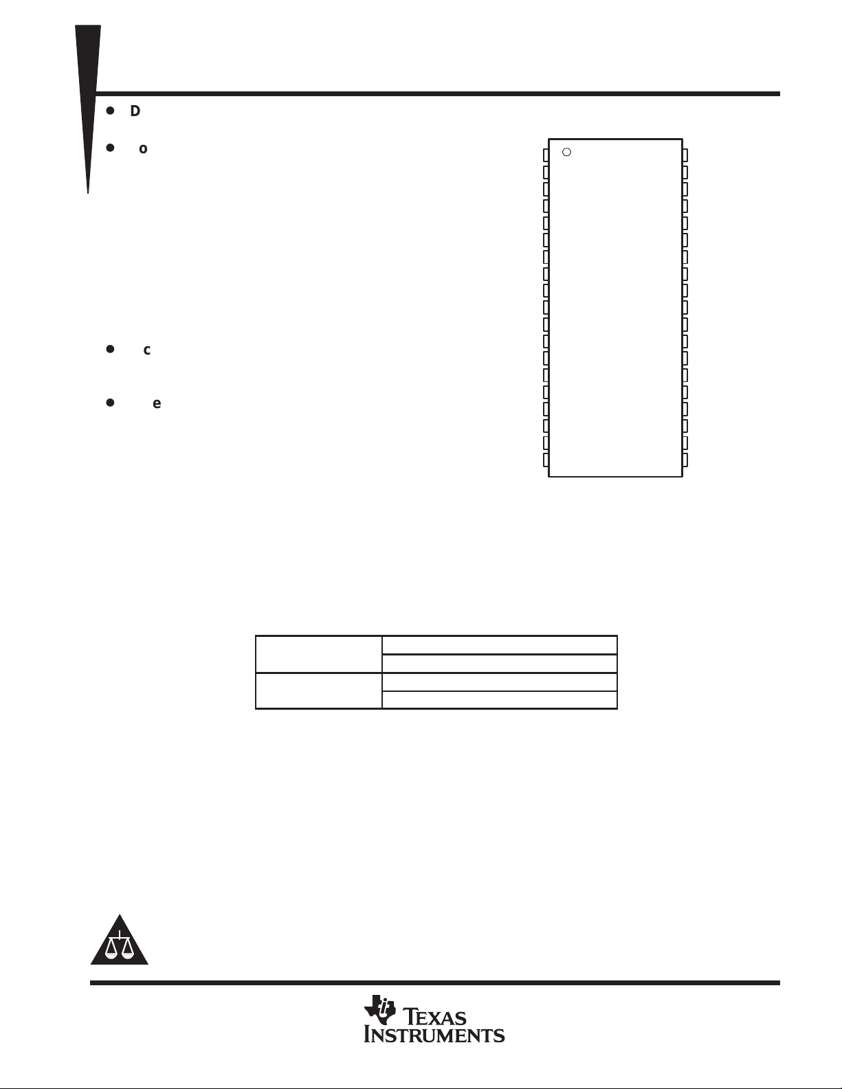
DB PACKAGE
(TOP VIEW)
1
2
3
4
5
6
7
8
9
10
11
12
13
14
15
16
17
18
19
VCO_1 V
38
R
37
BIAS
VCOIN_1
36
VCO_1 GND
35
VCO_1 INHIBIT
34
PFD_1 INHIBIT
33
NC
32
GND
31
NC
30
NC
29
NC
28
GND
27
VCO_2 V
26
R
25
BIAS
VCOIN_2
24
VCO_2 GND
23
VCO_2 INHIBIT
22
PFD_2 INHIBIT
21
NC
20
The TLC2943 is a multichip module product that
uses two TLC2933 chips. The TLC2933 chip is
composed of a voltage-controlled oscillator (VCO) and an edge-triggered-type phase frequency detector
(PFD). The oscillation frequency range of the VCO is set by an external bias resistor (R BIAS ). The high-speed
PFD with internal charge pump detects the phase difference between the reference frequency input and signal
frequency input from the external counter. Both the VCO and the PFD have inhibit functions that can be used
as a power-down mode. The high-speed and stable VCO characteristics of the TLC2933 make the TLC2943
suitable for use in dual high-performance phase-locked loop (PLL) systems.
DD
_1
DD
_2
°
–
Please be aware that an important notice concerning availability, standard warranty, and use in critical applications of
Texas Instruments semiconductor products and disclaimers thereto appears at the end of this data sheet.
PRODUCTION DATA information is current as of publication date.
Products conform to specifications per the terms of Texas Instruments
standard warranty. Production processing does not necessarily include
testing of all parameters.
AVAILABLE OPTIONS
A
°
TLC2943IDBR (Tape and Reel)
PACKAGE
SMALL OUTLINE (DB)
TLC2943IDB
Copyright 1999, Texas Instruments Incorporated
POST OFFICE BOX 655303 • DALLAS, TEXAS 75265
1
TLC2943
HIGH-PERFORMANCE DUAL PHASE-LOCKED BUILDING BLOCK
SLAS249 – NOVEMBER 1999
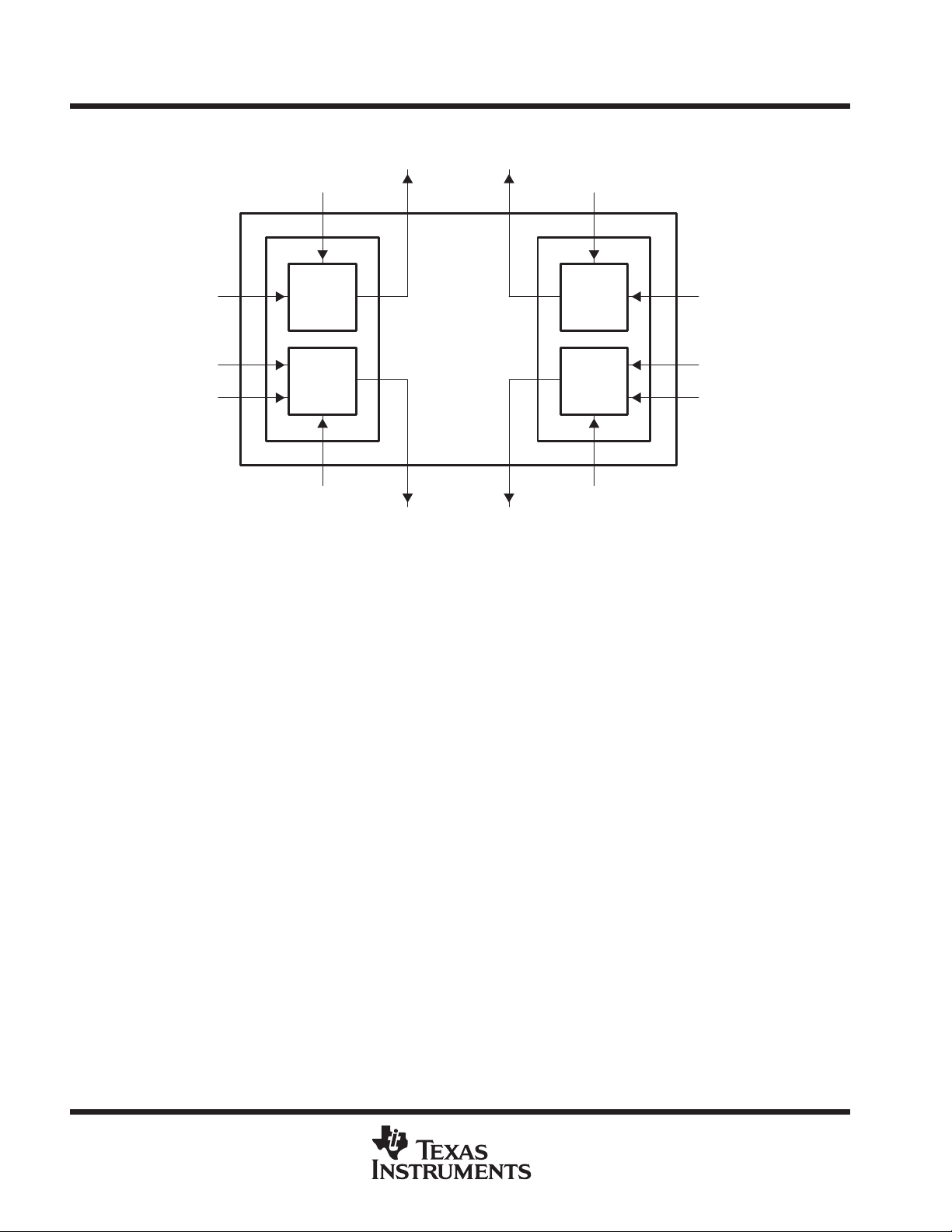
functional block diagram
VCOIN_1
FIN-A_1
FIN-B_1
VCO_1 INHIBIT
VCO_1
PFD_1
PFD_1 INHIBIT
VCO_1 OUT
PFD_1 OUT
VCO_2 OUT
PFD_2 OUT
VCO_2 INHIBIT
VCO_2
PFD_2
PFD_2 INHIBIT
VCOIN_2
FIN-A_2
FIN-B_2
2
POST OFFICE BOX 655303 • DALLAS, TEXAS 75265
TLC2943
I/O
DESCRIPTION
GND
HIGH-PERFORMANCE DUAL PHASE-LOCKED BUILDING BLOCK
SLAS249 – NOVEMBER 1999
Terminal Functions
TERMINAL
NAME NO.
8, 31 Common GND for chip 1
12, 27 Common GND for chip 2
FIN–A_1,
FIN–B_1
FIN–A_2,
FIN–B_2
LOGIC_1 GND 7 Ground for the internal logic of chip 1
LOGIC_2 GND 19 Ground for the internal logic of chip 2
LOGIC_1 V
LOGIC_2 V
NC
PFD_1 INHIBIT 33 I
PFD_2 INHIBIT 21 I
PFD_1 OUT 6 O PFD output of chip 1. When the PFD_1 INHIBIT is high, PFD_1 OUT is in the high-impedance state.
PFD_2 OUT 18 O PFD output of chip 2. When the PFD_2 INHIBIT is high, PFD_2 OUT is in the high-impedance state.
R
BIAS
R
BIAS
TEST_1 2 Test terminal. TEST connects to LOGIC_1 GND for normal operation.
TEST_2 14 Test terminal. TEST connects to LOGIC_2 GND for normal operation.
VCO_1 GND 35 GND for VCO_1
VCO_2 GND 23 GND for VCO_2
VCO_1 INHIBIT 34 I VCO inhibit control for chip 1. When VCO_1 INHIBIT is high, VCO_1 OUT is low (see Table 1).
VCO_2 INHIBIT 22 I VCO inhibit control for chip 2. When VCO_2 INHIBIT is high, VCO_2 OUT is low (see Table 1).
VCO_1 OUT 3 O VCO output of chip 1. When VCO_1 INHIBIT is high, VCO_1 OUT is low.
VCO_2 OUT 15 O VCO output of chip 2. When VCO_2 INHIBIT is high, VCO_2 OUT is low.
VCO_1 V
VCO_2 V
VCOIN_1 36 I
VCOIN_2 24 I
DD
DD
_1 37 I
_2 25 I
DD
DD
4
5
16
17
1
13
9, 10,
11, 20,
28, 29,
30, 32
38
26
Reference frequency signal input and comparison frequency signal input for PFD_1. fREF–IN_1 inputs
to FIN-A_1, and comparison frequency input from external counter logic to FIN–B_1, for a lag-lead filter
I
use as LPF.
Reference frequency signal input and comparison frequency signal input for PFD_2. fREF–IN_2 inputs
to FIN-A_2, and comparison frequency input from external counter logic to FIN-B_2, for a lag-lead filter use
I
as LPF.
Power supply for the internal logic of chip 1. This power supply should be separate from VCO VDD to
reduce cross-coupling between supplies.
Power supply for the internal logic of chip 2. This power supply should be separate from VCO VDD to
reduce cross-coupling between supplies.
No internal connection
PFD inhibit control for chip 1. When PFD_1 INHIBIT is high, PFD_1 OUT is in the high-impedance state,
see Table 2.
PFD inhibit control for chip 2. When PFD_2 INHIBIT is high, PFD_2 OUT is in the high-impedance state,
see Table 2.
Bias supply for VCO_1. An external resistor (R
adjusting the oscillation frequency range of VCO_1.
Bias supply for VCO_2. An external resistor (R
adjusting the oscillation frequency range of VCO_2.
Power supply for VCO_1. This power supply should be separate from LOGIC VDD to reduce
cross-coupling between supplies.
Power supply for VCO_2. This power supply should be separate from LOGIC VDD to reduce
cross-coupling between supplies.
VCO_1 control voltage input. Nominally the external loop filter output connects to VCO IN to control VCO
oscillation frequency .
VCO_2 control voltage input. Nominally the external loop filter output connects to VCO IN to control VCO
oscillation frequency .
) between VCO_1 VDD and BIAS_1 supplies bias for
BIAS
) between VCO_2 VDD and BIAS_2 supplies bias for
BIAS
POST OFFICE BOX 655303 • DALLAS, TEXAS 75265
3
TLC2943
HIGH-PERFORMANCE DUAL PHASE-LOCKED BUILDING BLOCK
SLAS249 – NOVEMBER 1999
detailed description
MCM (multichip module) technology for TLC2943
The TLC2943 is a multichip module (MCM) product that uses two TLC2933 chips. Inside the package, two chips
are completely isolated by a special formed lead-frame. Therefore,when using the TLC2943 in two
asynchronous PLL circuits, there is no performance degradation by electrical interference between chips inside
the package. So, the same performance as TLC2933 can be easily expected by using TLC2943.
The NC terminals in the middle on both sides of the package are to achieve complete isolation inside the
package. To get the best performance from this MCM technology, it is better to make a careful board layout of
the external power supply, ground, and signal lines.
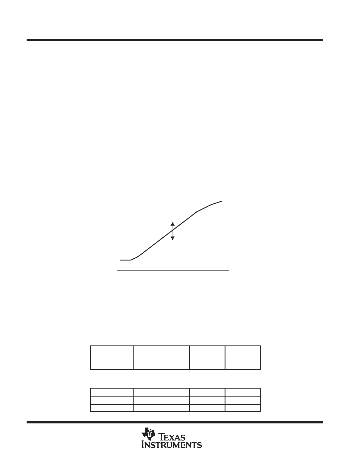
voltage controlled oscillator (VCO)
VCO_1 and VCO_2 have the same typical characteristics. Each VCO oscillation frequency is determined by
an external resistor (R
and range depend on this resistor value. The bias resistor value for the minimum temperature coefficient is
nominally 2.2 kΩ with V
the recommended operating conditions. Figure 1 shows the typical frequency variation and VCO control
voltage.
VCO Oscillation Frequency (f
) connected between the VCO VDD and the BIAS terminals. The oscillation frequency
BIAS
= 3.3 V and nominally 2.4 kΩ with VDD = 5 V . For the lock frequency range, refer to
DD
)
osc
VCO Oscillation Frequency Range
BIAS Resistor (R
VCO Control Voltage (V
BIAS)
COIN
)
Figure 1. VCO_1 and VCO_2 Oscillation Frequency
VCO inhibit function
Each VCO has an externally controlled inhibit function that inhibits the VCO output. The VCO oscillation is
stopped during a high level on VCOINHIBIT, so the high level can also be used as the power-down mode. The
VCO output maintains a low level during the power-down mode (see Table 1 and Table 2).
Table 1. VCO_1 Inhibit Function
VCO_1 INHIBIT VCO_1 OSCILLATOR VCO_1 OUT VCO_1 I
Low Active Active Normal
High Stop Low Power down
DD
Table 2. VCO_2 Inhibit Function
VCO_2 INHIBIT VCO_2 OSCILLATOR VCO_2 OUT VCO_2 I
Low Active Active Normal
High Stop Low Power down
4
POST OFFICE BOX 655303 • DALLAS, TEXAS 75265
DD
HIGH-PERFORMANCE DUAL PHASE-LOCKED BUILDING BLOCK
SLAS249 – NOVEMBER 1999
detailed description (continued)
phase frequency detector (PFD)
The PFD is a high-speed, edge-triggered detector with an internal charge pump. The PFD detects the phase
difference between two frequency inputs supplied to FIN-A and FIN-B as shown in Figure 2. Nominally the
reference is supplied to FIN-A, and the frequency from the external counter output is fed to FIN-B. For clock
recovery PLL systems, other types of phase detectors should be used.
FIN-A_1, 2
FIN-B_1, 2
VOH
PFD_1, 2 OUT
HI-Z
TLC2943
VOL
Figure 2. PFD Function Timing Chart
PFD output control
A high level on PFD INHIBIT places the PFD OUT in the high impedance state and the PFD stops phase
detection as shown in T able 3 and T able 4. A high level on PFD inhibit also can be used as the power-down mode
for the PFD.
Table 3. PFD_1 Inhibit Function
PFD_1 INHIBIT PFD_1 PFD_1 OUT PFD_1 I
Low Active Active Normal
High Stop Hi-Z Power down
DD
Table 4. PFD_2 Inhibit Function
PFD_2 INHIBIT PFD_2 PFD_2 OUT PFD_2 I
Low Active Active Normal
High Stop Hi-Z Power down
DD
POST OFFICE BOX 655303 • DALLAS, TEXAS 75265
5
TLC2943
HIGH-PERFORMANCE DUAL PHASE-LOCKED BUILDING BLOCK
SLAS249 – NOVEMBER 1999
internal function block diagram
BIAS
Resistor
VCO Control
V
COIN
FIN-A
FIN-B
BIAS
Circuit
Figure 3. VCO Block Schematic (VCO_1, VCO_2)
Detector
Figure 4. PFD Block Schematic (PFD_1, PFD_2)
Charge Pump
PFD OUT
Output
Buffer
VCO OUT
6
POST OFFICE BOX 655303 • DALLAS, TEXAS 75265
TLC2943
HIGH-PERFORMANCE DUAL PHASE-LOCKED BUILDING BLOCK
SLAS249 – NOVEMBER 1999
DD
†
+ 0.5 V. . . . . . . . . . . . . . . . . . . . . . . . . . . . . . . . . .
absolute maximum ratings over operating free-air temperature (unless otherwise noted)
Supply voltage (each supply), V
Input voltage range (each input), V
Input current (each input), I
I
(se e Note 1) 7 V. . . . . . . . . . . . . . . . . . . . . . . . . . . . . . . . . . . . . . . . . . . . . . . . . .
DD
(se e Note 1) –0.5 to V
I
±20 mA. . . . . . . . . . . . . . . . . . . . . . . . . . . . . . . . . . . . . . . . . . . . . . . . . . . . . . . . . . . . . . .
Output current (each output), IO ±20 mA. . . . . . . . . . . . . . . . . . . . . . . . . . . . . . . . . . . . . . . . . . . . . . . . . . . . . . . . . . . .
Continuous total power dissipation at (or below) T
= 25°C (see Note 2) 1160 mW. . . . . . . . . . . . . . . . . . . . . . . .
A
Operating free-air temperature range, TA –20°C to 75°C. . . . . . . . . . . . . . . . . . . . . . . . . . . . . . . . . . . . . . . . . . . . . .
Storage temperature range, T
Lead temperature 1,6 mm (1/16 in) from case for 10 seconds 260
†
Stresses beyond those listed under “absolute maximum ratings” may cause permanent damage to the device. These are stress ratings only, and
functional operation of the device at these or any other conditions beyond those indicated under “recommended operating conditions” is not
implied. Exposure to absolute-maximum-rated conditions for extended periods may affect device reliability.
NOTES: 1. All voltage values are with respect to network ground terminal.
2. For operation above 25°C free-air temperature, derate linearly at the rate of 9.3 mW/
–65°C to 150°C. . . . . . . . . . . . . . . . . . . . . . . . . . . . . . . . . . . . . . . . . . . . . . . . . . . .
stg
°C.
°C. . . . . . . . . . . . . . . . . . . . . . . . . . . . . . . . . . .
recommended operating conditions
MIN NOM MAX UNIT
VDD = 3 V 2.85 3 3.15
Supply voltage (each supply, see Notes 3 and 4 ), V
Input voltage range (input except for VCOIN_1, 2), V
Output current (each output), I
Control voltage, VCOIN 1 V
Clock frequency, f
Oscillation frequency range set resistor (each RBIAS), R
Top operating temperature range –20 75
NOTES: 3. It is recommended that the logic supply terminal (LOGIC VDD) and the VCO supply terminal (VCO VDD) be at the same voltage and
separated from each other.
4. Insert bypass capacitors locating the nearest point to each power supply terminal.
O
DD
I
BIAS
VCO
VDD = 3.3 V 3.15 3.3 3.45
VDD = 5 V 4.75 5 5.25
0 V
0 ±2 mA
VDD = 3 V 37 55
VDD = 3.3 V 37 60
VDD = 5 V 43 100
VDD = 3 V 1.8 2.7
VDD = 3.3 V 1.8 3.0
VDD = 5 V 2.2 3.0
DD
DD
V
V
V
MHz
kΩ
_
C
POST OFFICE BOX 655303 • DALLAS, TEXAS 75265
7
TLC2943
HIGH-PERFORMANCE DUAL PHASE-LOCKED BUILDING BLOCK
SLAS249 – NOVEMBER 1999
electrical characteristics over recommended operating free-air temperature range, VDD = 3 V
(unless otherwise noted)
VCO section
PARAMETER TEST CONDITIONS MIN NOM MAX UNIT
V
OH
V
OL
V
(TH+)
I
I
Z
(VCOIN)
I
DD(INH)
I
DD(VCO)
NOTES: 5. The current into VCO VDD and LOGIC VDD when VCO INHIBIT = VDD and PFD INHIBIT is high.
PFD section
V
OH
V
OL
I
OZ
V
IH
V
IL
V
(TH+)
C
I
Z
I
I
DD(PFD)
NOTE 7: The current into LOGIC VDD when FIN–A and FIN–B = 30 MHz (V I(PP) = 3 V , rectangular wave), PFD INHIBIT = GND, PFD OUT open,
High-level output voltage IOH = –2 mA 2.4 V
Low-level output voltage IOL = 2 mA 0.3 V
Positive input threshold voltage 0.9 1.5 2.1 V
Input current VI = VDD or GND ±1 µA
VCOIN input impedance VCOIN = 1/2V
VCO supply current (inhibit) (for one chip) See Note 5 0.01 1 µA
VCO supply current (for one chip) See Note 6 5.1 15 mA
6. The current into VCO VDD and LOGIC VDD when VCO IN = 1/2 VDD , R
is high.
PARAMETER TEST CONDITIONS MIN NOM MAX UNIT
High-level output voltage IOH = –2 mA 2.7 V
Low-level output voltage IOL = 2 mA 0.2 V
High-impedance state output current PFD INHIBIT = high, VO = VDD or GND ±1 µA
High-level input voltage at FIN–A, FIN–B 2.1 V
Low-level input voltage at FIN–A, FIN–B 0.9 V
Positive input threshold voltage at PFD
INHIBIT
Input capacitance at FIN–A, FIN–B 5 pF
Input impedance at FIN–A, FIN–B 10 MΩ
PFD supply current See Note 7 0.7 4 mA
and VCO OUT is inhibited.
BIAS
DD
= 2.4 kΩ, VCO INHIBIT = ground, and PFD INHIBIT
0.9 1.5 2.1 V
10 MΩ
8
POST OFFICE BOX 655303 • DALLAS, TEXAS 75265
TLC2943
HIGH-PERFORMANCE DUAL PHASE-LOCKED BUILDING BLOCK
SLAS249 – NOVEMBER 1999
electrical characteristics over recommended operating free-air temperature range, VDD = 3.3 V
(unless otherwise noted) (continued)
VCO section
PARAMETER TEST CONDITIONS MIN NOM MAX UNIT
V
OH
V
OL
V
(TH+)
I
I
Z
(VCOIN)
I
DD(INH)
I
DD(VCO)
NOTES: 5. The current into VCO VDD and LOGIC VDD when VCO INHIBIT = VDD and PFD INHIBIT is high.
PFD section
V
OH
V
OL
I
OZ
V
IH
V
IL
V
(TH+)
C
I
Z
I
I
DD(PFD)
NOTE 8: The current into LOGIC VDD when FIN–A and FIN–B = 30 MHz (V I(PP) = 3.3 V , rectangular wave), PFD INHIBIT = GND, PFD OUT
High-level output voltage IOH = –2 mA 2.7 V
Low-level output voltage IOL = 2 mA 0.4 V
Positive input threshold voltage 1 1.65 2.3 V
Input current VI = VDD or GND ±1 µA
VCOIN input impedance VCOIN = 1/2V
VCO supply current (inhibit) (for one chip) See Note 5 0.01 1 µA
VCO supply current (for one chip) See Note 6 6.2 16 mA
6. The current into VCO VDD and LOGIC VDD when VCO IN = 1/2 VDD , R
is high.
PARAMETER TEST CONDITIONS MIN NOM MAX UNIT
High-level output voltage IOH = –2 mA 3 V
Low-level output voltage IOL = 2 mA 0.2 V
High-impedance state output current PFD INHIBIT = high, VO = VDD or GND ±1 µA
High-level input voltage at FIN–A, FIN–B 2.3 V
Low-level input voltage at FIN–A, FIN–B 1 V
Positive input threshold voltage at PFD
INHIBIT
Input capacitance at FIN–A, FIN–B 5 pF
Input impedance at FIN–A, FIN–B 10 MΩ
PFD supply current See Note 8 0.8 5 mA
open, and VCO OUT is inhibited.
BIAS
DD
= 2.4 kΩ, VCO INHIBIT = ground, and PFD INHIBIT
10 MΩ
1 1.65 2.3 V
POST OFFICE BOX 655303 • DALLAS, TEXAS 75265
9

TLC2943
HIGH-PERFORMANCE DUAL PHASE-LOCKED BUILDING BLOCK
SLAS249 – NOVEMBER 1999
electrical characteristics over recommended operating free-air temperature range, VDD = 5 V
(unless otherwise noted) (continued)
VCO section
PARAMETER TEST CONDITIONS MIN NOM MAX UNIT
V
OH
V
OL
V
(TH+)
I
I
Z
(VCOIN)
I
DD(INH)
I
DD(VCO)
NOTES: 5. The current into VCO VDD and LOGIC VDD when VCO INHIBIT = VDD and PFD INHIBIT is high.
PFD section
V
OH
V
OL
I
OZ
V
IH
V
IL
V
(TH+)
C
I
Z
I
I
DD(PFD)
NOTE 9: The current into LOGIC VDD when FIN–A and FIN–B = 50 MHz (V I(PP) = 5 V , rectangular wave), PFD INHIBIT = GND, PFD OUT open,
High-level output voltage IOH = –2 mA 4.5 V
Low-level output voltage IOL = 2 mA 0.5 V
Positive input threshold voltage 1.5 2.5 3.5 V
Input current VI = VDD or GND ±1 µA
VCOIN input impedance VCOIN = 1/2V
VCO supply current (inhibit) (for one chip) See Note 5 0.01 1 µA
VCO supply current (for one chip) See Note 6 14 35 mA
6. The current into VCO VDD and LOGIC VDD when VCO IN = 1/2 VDD , R
is high.
PARAMETER TEST CONDITIONS MIN NOM MAX UNIT
High-level output voltage IOH = –2 mA 4.5 V
Low-level output voltage IOL = 2 mA 0.2 V
High-impedance state output current PFD INHIBIT = high, VO = VDD or GND ±1 µA
High-level input voltage at FIN–A, FIN–B 3.5 V
Low-level input voltage at FIN–A, FIN–B 1.5 V
Positive input threshold voltage at PFD
INHIBIT
Input capacitance at FIN–A, FIN–B 7 pF
Input impedance at FIN–A, FIN–B 10 MΩ
PFD supply current See Note 9 2.6 8 mA
and VCO OUT is inhibited.
BIAS
DD
= 2.4 kΩ, VCO INHIBIT = ground, and PFD INHIBIT
1.5 2.5 3.5 V
10 MΩ
10
POST OFFICE BOX 655303 • DALLAS, TEXAS 75265

HIGH-PERFORMANCE DUAL PHASE-LOCKED BUILDING BLOCK
ns
See Figure 6 and Figure 7, and Table 5
ns
C
See Figure 6
ns
SLAS249 – NOVEMBER 1999
operating characteristics at VDD = 3 V, TA = 25°C (unless otherwise noted)
VCO section
PARAMETER TEST CONDITIONS MIN NOM MAX UNIT
f
(OSC)
t
(STB)
t
r
t
f
f
(DUTY)
f
(TA)
f
(VDD)
NOTE 10: The time period to the stable VCO oscillation frequency after the VCO INHIBIT terminal is changed to a low level.
PFD section
f
MAX
t
PLZ
t
PHZ
t
PZL
t
PZH
t
r
t
f
Oscillation frequency R
Time to stable oscillation See Note 10 10 µs
Output rise time CL = 15 pF, See Figure 5 3.3 10 ns
Output fall time CL = 15 pF, See Figure 5 2 8 ns
Duty cycle R
Temperature coefficient of oscillation
frequency
Supply voltage coefficient of oscillation
frequency supply
PARAMETER TEST CONDITIONS MIN NOM MAX UNIT
Maximum operating frequency 30 MHz
PFD output disable time from low level 20 40
PFD output disable time from high level
PFD output enable time to low level
PFD output enable time to high level 4.8 18
Rise time
Fall time
= 2.4 kΩ, VCOIN = 1/2V
BIAS
= 2.4 kΩ, VCOIN = 1/2V
BIAS
R
= 2.4 kΩ,
BIAS
Top = –20°C to 75°C
R
= 2.4 kΩ,
BIAS
VDD = 2.85 V to 3.15 V
p
= 15 pF,
L
VCOIN = 1/2V
VCOIN = 1.5 V,
DD
DD
DD
38 48 58 MHz
45% 50% 55%
0.03 %/°C
0.04 %/mV
18 40
4.1 18
3.1 9
1.5 9
TLC2943
POST OFFICE BOX 655303 • DALLAS, TEXAS 75265
11

TLC2943
ns
See Figure 6 and Figure 7, and Table 5
ns
C
See Figure 6
ns
HIGH-PERFORMANCE DUAL PHASE-LOCKED BUILDING BLOCK
SLAS249 – NOVEMBER 1999
operating characteristics at VDD = 3.3 V, TA = 25°C (unless otherwise noted)
VCO section
PARAMETER TEST CONDITIONS MIN NOM MAX UNIT
f
(OSC)
t
(STB)
t
r
t
f
f
(DUTY)
f
(TA)
f
(VDD)
NOTE 10: The time period to the stable VCO oscillation frequency after the VCO INHIBIT terminal is changed to a low level.
PFD section
f
MAX
t
PLZ
t
PHZ
t
PZL
t
PZH
t
r
t
f
Oscillation frequency R
Time to stable oscillation See Note 10 10 µs
Output rise time CL = 15 pF, See Figure 5 3 8 ns
Output fall time CL = 15 pF, See Figure 5 1.9 7 ns
Duty cycle R
Temperature coefficient of oscillation
frequency
Supply voltage coefficient of oscillation
frequency supply
PARAMETER TEST CONDITIONS MIN NOM MAX UNIT
Maximum operating frequency 30 MHz
PFD output disable time from low level 20 40
PFD output disable time from high level
PFD output enable time to low level
PFD output enable time to high level 16
Rise time
Fall time
= 2.4 kΩ, VCOIN = 1/2V
BIAS
= 2.4 kΩ, VCOIN = 1/2V
BIAS
R
= 2.4 kΩ,
BIAS
Top = –20°C to 75°C
R
= 2.4 kΩ,
BIAS
VDD = 3.15 V to 3.45 V
p
= 15 pF,
L
VCOIN = 1/2V
VCOIN = 1.65 V,
DD
DD
DD
42 52 62 MHz
45% 50% 55%
0.03 %/°C
0.04 %/mV
18 40
16
8
8
12
POST OFFICE BOX 655303 • DALLAS, TEXAS 75265

HIGH-PERFORMANCE DUAL PHASE-LOCKED BUILDING BLOCK
ns
See Figure 6 and Figure 7, and Table 5
ns
C
See Figure 6
ns
operating characteristics at VDD = 5 V, TA = 25°C (unless otherwise noted)
VCO section
PARAMETER TEST CONDITIONS MIN NOM MAX UNIT
f
(OSC)
t
(STB)
t
r
t
f
f
(DUTY)
f
(TA)
f
(VDD)
PFD section
f
MAX
t
PLZ
t
PHZ
t
PZL
t
PZH
t
r
t
f
Oscillation frequency R
Time to stable oscillation See Note 10 10 µs
Output rise time CL = 15 pF, See Figure 5 2.1 5 ns
Output fall time CL = 15 pF, See Figure 5 1.5 4 ns
Duty cycle R
Temperature coefficient of oscillation
frequency
Supply voltage coefficient of oscillation
frequency supply
PARAMETER TEST CONDITIONS MIN NOM MAX UNIT
Maximum operating frequency 50 MHz
PFD output disable time from low level 20 40
PFD output disable time from high level
PFD output enable time to low level
PFD output enable time to high level 3.5 10
Rise time
Fall time
= 2.4 kΩ, VCOIN = 1/2V
BIAS
= 2.4 kΩ, VCOIN = 1/2V
BIAS
R
= 2.4 kΩ,
BIAS
Top = –20°C to 75°C
R
= 2.4 kΩ,
BIAS
VDD = 4.75 V to 5.25 V
p
= 15 pF,
L
VCOIN = 1/2V
VCOIN = 2.5 V,
DD
DD
DD
TLC2943
SLAS249 – NOVEMBER 1999
64 80 96 MHz
45% 50% 55%
0.03 %/°C
0.02 %/mV
17 40
3.7 10
1.7 5
1.3 5
POST OFFICE BOX 655303 • DALLAS, TEXAS 75265
13

TLC2943
HIGH-PERFORMANCE DUAL PHASE-LOCKED BUILDING BLOCK
SLAS249 – NOVEMBER 1999
PARAMETER MEASUREMENT INFORMATION
FIN-A
FIN-B
PFD INHIBIT
V
DD
GND
V
DD
GND
V
DD
GND
50%
VCO OUT
10%
90%
t
r
90%
10%
t
f
Figure 5. VCO Output Voltage Waveform (Each VCO)
50%
50%
50%
V
DD
GND
V
DD
GND
V
DD
GND
PFD OUT
V
DD
GND
t
PZH
10%
t
r
90%
50%
50%
t
PHZ
t
PZL
t
f
Figure 6. PFD Output Voltage Waveform
90%
50%
10%
50%
t
PLZ
V
DD
GND
14
POST OFFICE BOX 655303 • DALLAS, TEXAS 75265

TLC2943
1 kΩ
15 pF
HIGH-PERFORMANCE DUAL PHASE-LOCKED BUILDING BLOCK
SLAS249 – NOVEMBER 1999
PARAMETER MEASUREMENT INFORMATION
Test Point
S1
R
L
DUT
C
L
Figure 7. PFD Output Test Conditions
Table 5. PFD Output Test Conditions
S2
PARAMETER R
t
PZH
t
PHZ
t
r
t
PZL
t
PLZ
t
f
L
C
L
p
S1 S2
OPEN CLOSE
CLOSE OPEN
POST OFFICE BOX 655303 • DALLAS, TEXAS 75265
15

TLC2943
HIGH-PERFORMANCE DUAL PHASE-LOCKED BUILDING BLOCK
SLAS249 – NOVEMBER 1999
TYPICAL CHARACTERISTICS
OSCILLATION FREQUENCY
CONTROL VOLTAGE
120
VDD = 3.3 V
R
= 1.8 kΩ
BIAS
100
80
60
40
– Oscillation Frequency – MHz
osc
20
f
0
0.6 3.0 3.6
0.0
1.2 1.8 2.4
VCOIN – VCO Control Voltage – V
Figure 8
OSCILLATION FREQUENCY
CONTROL VOLTAGE
120
VDD = 3.3 V
R
= 2.7 kΩ
BIAS
100
vs
vs
– 20°C
25°C
75°C
OSCILLATION FREQUENCY
CONTROL VOLTAGE
120
VDD = 3.3 V
R
= 2.2 kΩ
BIAS
100
80
60
40
– Oscillation Frequency – MHz
osc
20
f
0
0.6 3.0 3.6
0.0
1.2 1.8 2.4
VCOIN – VCO Control Voltage – V
Figure 9
OSCILLATION FREQUENCY
CONTROL VOLTAGE
120
VDD = 3.3 V
R
= 3.0 kΩ
BIAS
100
vs
– 20°C
25°C
75°C
vs
80
60
75°C
25°C
40
– Oscillation Frequency – MHz
osc
20
f
0
16
0.6 3.0 3.6
0.0
VCOIN – VCO Control Voltage – V
– 20°C
1.2 1.8 2.4
Figure 10
80
60
40
– Oscillation Frequency – MHz
osc
20
f
0
0.0
POST OFFICE BOX 655303 • DALLAS, TEXAS 75265
75°C
25°C
– 20°C
0.6 3.0 3.6
1.2 1.8 2.4
VCOIN – VCO Control Voltage – V
Figure 11

TLC2943
HIGH-PERFORMANCE DUAL PHASE-LOCKED BUILDING BLOCK
SLAS249 – NOVEMBER 1999
TYPICAL CHARACTERISTICS
OSCILLATION FREQUENCY
CONTROL VOLTAGE
160
VDD = 5 V
R
140
120
100
80
60
– Oscillation Frequency – MHz
40
osc
f
20
0
0.0
= 2.2 kΩ
BIAS
123
VCOIN – VCO Control Voltage – V
Figure 12
OSCILLATION FREQUENCY
CONTROL VOLTAGE
160
VDD = 5 V
R
140
120
BIAS
= 2.7 kΩ
vs
vs
– 20°C
– 20°C
25°C
75°C
45
25°C
OSCILLATION FREQUENCY
CONTROL VOLTAGE
160
VDD = 5 V
R
140
120
100
80
60
– Oscillation Frequency – MHz
40
osc
f
20
0
0.0
= 2.4 kΩ
BIAS
123
VCOIN – VCO Control Voltage – V
Figure 13
OSCILLATION FREQUENCY
CONTROL VOLTAGE
160
VDD = 5 V
R
140
120
BIAS
= 3.0 kΩ
vs
25°C
– 20°C
75°C
45
vs
25°C
100
80
60
– Oscillation Frequency – MHz
40
osc
f
20
0
0.0
123
VCOIN – VCO Control Voltage – V
Figure 14
75°C
45
POST OFFICE BOX 655303 • DALLAS, TEXAS 75265
100
80
60
– Oscillation Frequency – MHz
40
osc
f
20
0
0.0
75°C
– 20°C
123
VCOIN – VCO Control Voltage – V
Figure 15
45
17

TLC2943
HIGH-PERFORMANCE DUAL PHASE-LOCKED BUILDING BLOCK
SLAS249 – NOVEMBER 1999
TYPICAL CHARACTERISTICS
LOCK FREQUENCY RANGE
BIAS RESISTANCE
65
60
55
50
45
40
– Lock Frequency Range – MHz
LOCK
35
f
30
1.8 k
2.2 k 2.4 k
R
– BIAS Resistance – Ω
BIAS
Figure 16
vs
VDD = 3.15 V – 3.45 V
TA = –20°C to 75°C
2.7 k 3 k
LOCK FREQUENCY RANGE
BIAS RESISTANCE
110
100
90
80
70
60
– Lock Frequency Range – MHz
50
LOCK
40
f
30
2.2 k
2.4 k 2.6 k
R
– BIAS Resistance – Ω
BIAS
Figure 17
vs
VDD = 4.75 V – 5.25 V
TA = –20°C to 75°C
2.8 k 3 k
18
POST OFFICE BOX 655303 • DALLAS, TEXAS 75265

TLC2943
HIGH-PERFORMANCE DUAL PHASE-LOCKED BUILDING BLOCK
SLAS249 – NOVEMBER 1999
APPLICATION INFORMATION
gain of VCO and PFD
Figure 18 is a block diagram of the PLL. The
divider N value depends on the input frequency
and the desired VCO output frequency according
to the system application requirements. The K
and KV values are obtained from the operating
characteristics of the device as shown in
Figure 18. Kp is defined from the phase detector
VOL and VOH specifications and the equation
shown in Figure 18(b). KV is defined from
Figures 8, 9, 10, and 1 1 as shown in Figure 18(c).
The parameters for the block diagram with the
units are as follows:
KV : VCO gain (rad/s/V)
Kp : PFD gain (V/rad)
Kf : LPF gain (V/V)
K
: countdown divider gain (1/N)
N
external counter
When a large N counter is required by the
application, there is a possibility that the PLL
response becomes slow due to the counter
response delay time. In the case of a high
frequency application, the counter delay time
should be accounted for in the overall PLL design.
p
–2π 2π–π 0 π
Divider
(KN = 1/N)
f REF
Range of
Comparison
VOH – V
Kp =
4π
OL
PFD
(Kp)
TLC2933
V
OH
V
OL
LPF
(Kf)
(a)
f
MAX
f
MIN
KV =
VCO
(KV)
V
OH
VIN
VIN
MIN
2π(f
MAX
MAX
(c)(b)
VIN
– f
– VIN
Figure 18. Example of a PLL Block Diagram
MIN
MAX
)
MIN
R
BIAS
The external bias resistor sets the VCO center frequency with 1/2 V
applied to the VCO IN terminal. For the
DD
most accurate results, a metal-film resistor is the better choice, but a carbon-composition resistor can also be
used with excellent results. A 0.22 µF capacitor should be connected from the BIAS terminal to ground as close
to the device terminals as possible.
hold-in range
From the technical literature, the maximum hold-in range for an input frequency step for the three types of filter
configurations shown in Figure 17 is as follows:
Ǔǒ
Where
DwH]
0.8ǒK
p
Ǔǒ
K
Kf(R)
V
Kf (∞) = the filter transfer function value at ω = ∞
Ǔ
(1)
POST OFFICE BOX 655303 • DALLAS, TEXAS 75265
19

TLC2943
HIGH-PERFORMANCE DUAL PHASE-LOCKED BUILDING BLOCK
SLAS249 – NOVEMBER 1999
APPLICATION INFORMATION
low-pass-filter (LPF) configurations
References that include detailed design information about LPFs should be consulted for additional information.
Lag-lead filters or active filters are often used. Examples of LPFs are shown in Figure 19. When the active filter
of Figure 19(c) is used, the reference should be applied to FIN-B because of the amplifier inversion. Also, in
practical filter implementations, C2 is used as additional filtering at the VCO input. The value of C2 should be
equal to or less than one tenth the value of C1.
V
R1
I
T1 = C1R1
(a) LAG FILTER
C1
V
O
V
R1
I
T1 = C1R1
T2 = C1R2
(b) LAG-LEAD FILTER
R2
C1
C2
V
O
V
I
R1
(c) ACTIVE FILTER
R2
–
C2
A
C1
T1 = C1R1
T2 = C1R2
V
O
Figure 19. LPF Examples for PLL
passive filter
The transfer function for the low-pass filter shown in Figure 17(b) is;
V
O
V
IN
+
1)s
1)s T2
(
T1)T2
)
Where
T1+R1 C1 and T2+R2 C1
Using this filter makes the closed-loop PLL system a type 1 second-order system. The response curves of this
system to a unit step are shown in Figure 20.
active filter
When using the active filter shown in Figure 19(c), the phase detector inputs must be reversed, since the filter
adds an additional inversion. Therefore, the input reference frequency should be applied to the FIN-B terminal
and the output of the VCO divider should be applied to the input reference terminal, FIN-A.
The transfer function for the active filter shown in Figure 19(c) is:
F(s)
Using this filter makes the closed-loop PLL system a type 2 second-order system. The response curves of this
system to a unit step are shown in Figure 21.
1)s R2 C1
+
s R1 C1
(2)
(3)
20
POST OFFICE BOX 655303 • DALLAS, TEXAS 75265

TLC2943
HIGH-PERFORMANCE DUAL PHASE-LOCKED BUILDING BLOCK
SLAS249 – NOVEMBER 1999
APPLICATION INFORMATION
Using the lag-lead filter in Figure 19(b) and divider N value, the transfer function for phase and frequency are
shown in equations 4 and 5. Note that the transfer function for phase differs from the transfer function for
frequency by only the divider N value. The difference arises from the fact that the feedback for phase is unity,
while the feedback for frequency is 1/N.
Hence, the transfer function of Figure 19(a) for phase is
ȱ
Kp
K
F
2(s)
+
F
1(s)
and the transfer function for frequency is
N
(T1)T2
ȧ
ȧ
V
ȧ
)
ȧ
s2)
sƪ1
Ȳ
1)s T2
Kp
)
KV
N (T1)T2)
T2
ƫ
)
N (T1)T2)
K
p
ȱ
F
OUT(s)
F
REF(s)
The standard 2-pole denominator is D = s2 + 2 ζ ωn s + ω
of equation (4) and (5) with the standard 2-pole denominator gives the following results.
wn+
Solving for T1 + T2
K
+
(
Ǹ
T1)T2
K
ȧ
p
T1)T2
ȧ
V
ȧ
)
ȧ
Ȳ
Kp
N (T1)T2)
Kp
+
N w
s2)s
K
V
K
V
2
n
ƪ
1
)
1)s T2
K
KV
p
N (T1)T2)
T2
Kp
ƫ
)
N (T1)T2)
2
and comparing the coefficients of the denominator
n
K
ȳ
ȧ
ȧ
ȧ
K
ȧ
V
ȴ
ȳ
ȧ
ȧ
ȧ
ȧ
V
ȴ
(4)
(5)
(6)
and by using this value for T1 + T2 in equation (6) the damping factor is
w
n
z
+
ǒ
2
solving for T2
2
T2
+
then by substituting for T2 in equation (6)
KV
T1
+
N w
T2
z
N
–
w
Kp
K
p
–
2
n
)
K
Kp
V
2
z
w
n
N
Ǔ
K
V
N
)
Kp
K
V
POST OFFICE BOX 655303 • DALLAS, TEXAS 75265
(7)
(8)
(9)
21

TLC2943
HIGH-PERFORMANCE DUAL PHASE-LOCKED BUILDING BLOCK
SLAS249 – NOVEMBER 1999
APPLICATION INFORMATION
From the circuit constants and the initial design parameters then
2
ƪ
ȱ
ȧ
Ȳ
z
w
n
Kp
2
w
n
R2
+
R1
+
The capacitor, C1, is usually chosen between 1 µF and 0.1 µF to allow for reasonable resistor values and
physical capacitor size.
*
Kp
K
v
N
*
N
2
w
1
ƫ
K
C1
V
z
)
Kp
n
ȳ
N
1
ȧ
K
C1
V
ȴ
(10)
(11)
22
POST OFFICE BOX 655303 • DALLAS, TEXAS 75265

1.9
1.8
1.7
1.6
1.5
1.4
1.3
1.2
1.1
= 0.6
z
= 0.7
z
= 0.8
z
TLC2943
HIGH-PERFORMANCE DUAL PHASE-LOCKED BUILDING BLOCK
SLAS249 – NOVEMBER 1999
APPLICATION INFORMATION
= 0.1
z
= 0.2
z
= 0.3
z
= 0.4
z
= 0.5
z
1
0.9
= 1.0
z
0.8
Normalized Gain Response
0.7
0.6
0.5
0.4
0.3
0.2
0.1
0
012345678910111213
= 1.5
z
= 2.0
z
ωnts = 4.5
ω
nt
Figure 20. Type 1 Second-Order Step Response
POST OFFICE BOX 655303 • DALLAS, TEXAS 75265
23

TLC2943
HIGH-PERFORMANCE DUAL PHASE-LOCKED BUILDING BLOCK
SLAS249 – NOVEMBER 1999
APPLICATION INFORMATION
1.9
1.8
1.7
1.6
1.5
1.4
1.3
1.2
1.1
1
0.9
0.8
Normalized Gain Response
0.7
ζ = 0.1
ζ = 0.2
ζ = 0.3
ζ = 0.4
ζ = 0.5
ζ = 0.6
ζ = 0.7
ζ = 0.8
ζ = 1.0
ζ = 2.0
0.6
0.5
0.4
0.3
0.2
0.1
0
012345678910111213
ω
nt
Figure 21. Type 2 Second-Order Step Response
24
POST OFFICE BOX 655303 • DALLAS, TEXAS 75265

HIGH-PERFORMANCE DUAL PHASE-LOCKED BUILDING BLOCK
SLAS249 – NOVEMBER 1999
APPLICATION INFORMATION
PCB layout considerations
The TLC2943 contains high frequency analog oscillators; therefore, very careful breadboarding and
printed-circuit-board (PCB) layout is required for evaluation.
The following design recommendations benefit the TLC2943 user:
D
External analog and digital circuitry should be physically separated and shielded as much as possible to
reduce system noise.
D
RF breadboarding or RF PCB techniques should be used throughout the evaluation and production
process.
D
Wide ground leads or a ground plane should be used on the PCB layouts to minimize parasitic inductance
and resistance. The ground plane is the better choice for noise reduction.
D
LOGIC VDD and VCO VDD should be separate PCB traces and connected to the best filtered supply point
available in the system to minimize supply cross-coupling.
D
VCO VDD to GND and LOGIC VDD to GND should be decoupled with a 0.1-µF capacitor placed as close
as possible to the appropriate device terminals.
TLC2943
D
The no-connection (NC) terminal on the package should be connected to GND.
The evaluation and operation schematic for the TLC2943 is shown in Figure 22.
V
REF IN
DGND
Divide
By
N
DD
DGND
1
LOGIC VDD (digital)
2
TEST
3
VCO OUT
FIN–A
4
5
FIN–B
PFD OUT
6
7
LOGIC GND (Digital)
PLL1
Phase
Comparator
PLL2
VCO
VCO V
DD
BIAS
VCOIN
VCO GND
VCOINHIBIT
PFD INHIBIT
GND
38
37
36
35
34
33
31
†
R1
0.22 µF
AGND
S1
S2
AV
DD
R3
R2C2
C1
DGND
R5 R6
†
R
resistor
BIAS
DV
DD
Figure 22. Evaluation and Operation Schematic
POST OFFICE BOX 655303 • DALLAS, TEXAS 75265
25

TLC2943
HIGH-PERFORMANCE DUAL PHASE-LOCKED BUILDING BLOCK
SLAS249 – NOVEMBER 1999
MECHANICAL DATA
DB (R-PDSO-G**) PLASTIC SMALL-OUTLINE PACKAGE
28 PINS SHOWN
0,65
28
1
2,00 MAX
0,38
0,22
15
14
A
0,05 MIN
0,15
5,60
5,00
M
8,20
7,40
Seating Plane
0,10
0,15 NOM
Gage Plane
0°–8°
0,25
1,03
0,63
PINS **
DIM
A MAX
A MIN
NOTES: A. All linear dimensions are in millimeters.
B. This drawing is subject to change without notice.
C. Body dimensions do not include mold flash or protrusion not to exceed 0,15.
D. Falls within JEDEC MO-150
8
3,30
2,70
14
6,50
6,50
5,905,90
2016
7,50
6,90
24
8,50
28
10,50
9,907,90
30
10,50
9,90
38
12,90
12,30
4040065 /C 10/95
26
POST OFFICE BOX 655303 • DALLAS, TEXAS 75265

IMPORTANT NOTICE
T exas Instruments and its subsidiaries (TI) reserve the right to make changes to their products or to discontinue
any product or service without notice, and advise customers to obtain the latest version of relevant information
to verify, before placing orders, that information being relied on is current and complete. All products are sold
subject to the terms and conditions of sale supplied at the time of order acknowledgement, including those
pertaining to warranty, patent infringement, and limitation of liability.
TI warrants performance of its semiconductor products to the specifications applicable at the time of sale in
accordance with TI’s standard warranty. Testing and other quality control techniques are utilized to the extent
TI deems necessary to support this warranty . Specific testing of all parameters of each device is not necessarily
performed, except those mandated by government requirements.
CERTAIN APPLICA TIONS USING SEMICONDUCTOR PRODUCTS MA Y INVOLVE POTENTIAL RISKS OF
DEATH, PERSONAL INJURY, OR SEVERE PROPERTY OR ENVIRONMENTAL DAMAGE (“CRITICAL
APPLICATIONS”). TI SEMICONDUCTOR PRODUCTS ARE NOT DESIGNED, AUTHORIZED, OR
WARRANTED TO BE SUITABLE FOR USE IN LIFE-SUPPORT DEVICES OR SYSTEMS OR OTHER
CRITICAL APPLICA TIONS. INCLUSION OF TI PRODUCTS IN SUCH APPLICATIONS IS UNDERST OOD TO
BE FULLY AT THE CUSTOMER’S RISK.
In order to minimize risks associated with the customer’s applications, adequate design and operating
safeguards must be provided by the customer to minimize inherent or procedural hazards.
TI assumes no liability for applications assistance or customer product design. TI does not warrant or represent
that any license, either express or implied, is granted under any patent right, copyright, mask work right, or other
intellectual property right of TI covering or relating to any combination, machine, or process in which such
semiconductor products or services might be or are used. TI’s publication of information regarding any third
party’s products or services does not constitute TI’s approval, warranty or endorsement thereof.
Copyright 1999, Texas Instruments Incorporated
 Loading...