

CLOCK-TO-CUTOFF
FREQUENCY RATIO
查询TLC04/MF4A-50供应商
TLC04/MF4A-50, TLC14/MF4A-100
BUTTERWORTH FOURTH-ORDER LOW-PASS
SWITCHED-CAPACITOR FILTERS
SLAS021A – NOVEMBER 1986 – REVISED MARCH 1995
D
Low Clock-to-Cutoff-Frequency Ratio Error
TLC04/MF4A-50...±0.8%
TLC14/MF4A-100 . . . ±1%
D
Filter Cutoff Frequency Dependent Only on
External-Clock Frequency Stability
D
Minimum Filter Response Deviation Due to
External Component Variations Over Time
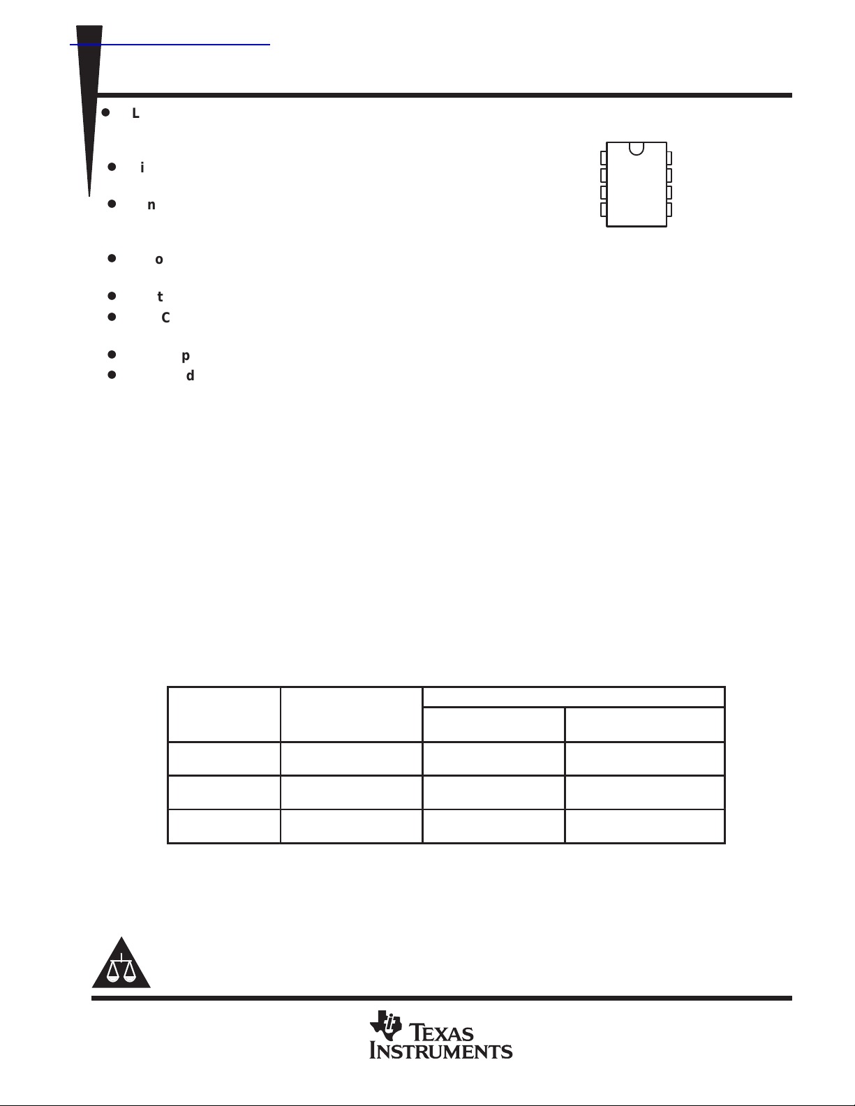
D OR P PACKAGE
(TOP VIEW)
CLKIN
CLKR
LS
V
CC–
1
2
3
4
FILTER IN
8
V
7
CC+
AGND
6
FILTER OUT
5
and Temperature
D
Cutoff Frequency Range From 0.1 Hz
to 30 kHz, V
D
5-V to 12-V Operation
D
Self Clocking or TTL-Compatible and
CC±
= ±2.5 V
CMOS-Compatible Clock Inputs
D
Low Supply-Voltage Sensitivity
D
Designed to be Interchangeable With
National MF4-50 and MF4-100
description
The TLC04/MF4A-50 and TLC14/MF4A-100 are monolithic Butterworth low-pass switched-capacitor filters.
Each is designed as a low-cost, easy-to-use device providing accurate fourth-order low-pass filter functions in
circuit design configurations.
Each filter features cutoff frequency stability that is dependent only on the external-clock frequency stability . The
cutoff frequency is clock tunable and has a clock-to-cutoff frequency ratio of 50:1 with less than ±0. 8% error
for the TLC04/MF4A-50 and a clock-to-cutoff frequency ratio of 100:1 with less than ±1% error for the
TLC14/MF4A-100. The input clock features self-clocking or TTL- or CMOS-compatible options in conjunction
with the level shift (LS) terminal.
The TLC04C/MF4A-50C and TLC14C/MF4A-100C are characterized for operation from 0°C to 70°C. The
TLC04I/MF4A-50I and TLC14I/MF4A-100I are characterized for operation from –40°C to 85°C. The
TLC04M/MF4A-50M and TLC14M/MF4A-100M are characterized over the full military temperature range of
–55°C to 125°C.
PRODUCTION DATA information is current as of publication date.
Products conform to specifications per the terms of Texas Instruments
standard warranty. Production processing does not necessarily include
testing of all parameters.
AVAILABLE OPTIONS
PACKAGE
T
A
0°C to 70°C
–40°C to 85°C
–55°C to 125°C
The D package is available taped and reeled. Add the suffix R to the device type (e.g., TLC04CDR/MF4A-50CDR).
Please be aware that an important notice concerning availability, standard warranty, and use in critical applications of
Texas Instruments semiconductor products and disclaimers thereto appears at the end of this data sheet.
50:1
100:1
50:1
100:1
50:1
100:1
POST OFFICE BOX 655303 • DALLAS, TEXAS 75265
SMALL OUTLINE PLASTIC DIP
(D) (P)
TLC04CD/MF4A-50CD
TLC14CD/MF4A-100CD
TLC04ID/MF4A-50ID
TLC14ID/MF4A-100ID
TLC04CP/MF4A-50CP
TLC14CP/MF4A-100CP
TLC04IP/MF4A-50IP
TLC14IP/MF4A-100IP
TLC04MP/MF4A-50MP
TLC14MP/MF4A-100MP
Copyright 1995, Texas Instruments Incorporated
1
TLC04/MF4A-50, TLC14/MF4A-100
I/O
DESCRIPTION
BUTTERWORTH FOURTH-ORDER LOW-PASS
SWITCHED-CAPACITOR FILTERS
SLAS021A – NOVEMBER 1986 – REVISED MARCH 1995
functional block diagram
3
LS
Level Shift
CLKIN
CLKR
1
2
Nonoverlapping
Clock Generator
φ2φ1
FILTER IN
AGND
8
6
Butterworth
Fourth-Order
Low-Pass Filter
5
FILTER OUT
Terminal Functions
TERMINAL
NAME NO.
AGND 6 I Analog ground. The noninverting input to the operational amplifiers of the Butterworth fourth-order low-pass filter.
CLKIN 1 I Clock in. CLKIN is the clock input terminal for CMOS-compatible clock or self-clocking options. For either option,
CLKR 2 I Clock R. CLKR is the clock input for a TTL-compatible clock. For a TTL clock, LS is connected to midsupply and
FILTER IN 8 I Filter input
FILTER OUT 5 O Butterworth fourth-order low-pass filter output
LS 3 I Level shift. LS accommodates the various input clocking options. For CMOS-compatible clocks or self-clocking,
V
V
CC+
CC–
7 I Positive supply voltage terminal
4 I Negative supply voltage terminal
LS is at V
from CLKIN to ground.
CLKIN can be left open, but it is recommended that it be connected to either V
LS is at V
. For self-clocking, a resistor is connected between CLKIN and CLKR and a capacitor is connected
CC–
and for TTL-compatible clocks, LS is at midsupply.
CC–
CC+
or V
CC–
.
2
POST OFFICE BOX 655303 • DALLAS, TEXAS 75265
UNIT
Clock frequenc
f
(see Note 2)
H
PARAMETER
TEST CONDITIONS
UNIT
VOMPeak output voltage
R
kΩ
V
IOSShort-circuit output current
T
25°C
See Note 4
mA
TLC04/MF4A-50, TLC14/MF4A-100
BUTTERWORTH FOURTH-ORDER LOW-PASS
SWITCHED-CAPACITOR FILTERS
SLAS021A – NOVEMBER 1986 – REVISED MARCH 1995
absolute maximum ratings over operating free-air temperature range (unless otherwise noted)
Supply voltage range, V
Operating free-air temperature range, T
(see Note 1) ±7 V. . . . . . . . . . . . . . . . . . . . . . . . . . . . . . . . . . . . . . . . . . . . . . . . . . . . .
CC±
: TLC04C/MF4A-50C, TLC14C/MF4A-100C 0°C to 70°C. . . . . .
A
†
TLC04I/MF4A-50I, TLC14I/MF4A-100I –40°C to 85°C. . . . . . . .
TLC04M/MF4A-50M, TLC14M/MF4A-100M –55°C to 125°C. . .
Storage temperature range, T
–65°C to 150°C. . . . . . . . . . . . . . . . . . . . . . . . . . . . . . . . . . . . . . . . . . . . . . . . . . .
stg
Lead temperature 1,6 mm (1/16 inch) from case for 10 seconds 260°C. . . . . . . . . . . . . . . . . . . . . . . . . . . . . . .
†
Stresses beyond those listed under “absolute maximum ratings” may cause permanent damage to the device. These are stress ratings only, and
functional operation of the device at these or any other conditions beyond those indicated under “recommended operating conditions” is not
implied. Exposure to absolute-maximum-rated conditions for extended periods may affect device reliability.
NOTE 1: All voltage values are with respect to the AGND terminal.
recommended operating conditions
TLC04/MF4A-50 TLC14/MF4A-100
MIN MAX MIN MAX
Positive supply voltage, V
Negative supply voltage, V
High-level input voltage, V
Low-level input voltage, V
y,
Cutoff frequency, fco (see Note 3) 0.1 40x10
Operating free-air temperature, T
NOTES: 2. Above 250 kHz, the input clock duty cycle should be 50% to allow the operational amplifiers the maximum time to settle while
processing analog samples.
3. The cutoff frequency is defined as the frequency where the response is 3.01 dB less than the dc gain of the filter.
clock
CC+
CC–
IH
IL
V
= ±2.5 V 5 1.5x10
A
CC±
V
= ±5 V 5 2x10
CC±
TLC04C/MF4A-50C, TLC14C/MF4A-100C 0 70 0 70
TLC04I/MF4A-50I, TLC14I/MF4A-100I –40 85 –40 85
TLC04M/MF4A-50M, TLC14M/MF4A-100M –55 125 –55 125
2.25 6 2.25 6 V
–2.25 –6 –2.25 –6 V
2 2 V
0.8 0.8 V
6
6
3
5 1.5x10
5 2x10
0.05 20x10
6
6
3
Hz
°C
z
electrical characteristics over recommended operating free-air temperature range, V
V
= –2.5 V, f
CC–
filter section
V
Output offset voltage 25 50 mV
OO
p
I
Supply current f
CC
‡
All typical values are at TA = 25°C.
NOTE 4: I
OS(source)
I
OS(sink)
is measured by forcing the output to its maximum negative voltage and then shorting the output to the V
≤ 250 kHz (unless otherwise noted)
clock
TLC04/MF4A-50 TLC14/MF4A-100
MIN
V
OM+
V
OM–
p
is measured by forcing the output to its maximum positive voltage and then shorting the output to the V
Source
Sink
= 10
L
°
,
=
A
= 250 kHz 1.2 2.25 1.2 2.25 mA
clock
1.8 2 1.8 2
–1.25 –1.7 –1.25 –1.7
‡
TYP
MAX MIN
–0.5 –0.5
4 4
TYP
‡
CC+
MAX
CC+
= 2.5 V,
terminal
CC –
terminal.
POST OFFICE BOX 655303 • DALLAS, TEXAS 75265
3
TLC04/MF4A-50, TLC14/MF4A-100
PARAMETER
UNIT
VOMPeak output voltage
R
kΩ
V
IOSShort-circuit output current
A
,
mA
V
Positive-going input threshold voltage
V
V
Negative-going input threshold voltage
CLKIN
V
V
Hysteresis voltage (V
V
)
V
VOHHigh-level output voltage
I
10 µA
V
VOLLow-level output voltage
I
A
V
Input leakage current
CLKR
y,
A
mA
IOOutput current
mA
BUTTERWORTH FOURTH-ORDER LOW-PASS
SWITCHED-CAPACITOR FILTERS
SLAS021A – NOVEMBER 1986 – REVISED MARCH 1995
electrical characteristics over recommended operating free-air temperature range, V
V
= –5 V, f
CC –
filter section
V
Output offset voltage 150 200 mV
OO
p
I
Supply current f
CC
k
Supply voltage sensitivity (see Figures 1 and 2) –30 –30 dB
SVS
†
All typical values are at TA = 25°C.
NOTE 4: I
OS(source)
is measured by forcing the output to its maximum negative voltage and then shorting the output to the V
clocking section
IT+
IT–
hys
p
p
†
All typical values are at TA = 25°C.
≤ 250 kHz (unless otherwise noted)
clock
TEST
CONDITIONS
V
OM+
V
OM–
p
is measured by forcing the output to its maximum positive voltage and then shorting the output to the V
PARAMETER TEST CONDITIONS MIN TYP†MAX UNIT
p
p
–
IT+
p
p
Source
Sink
IT–
= 10
L
T
= 25°C,
See Note 4
= 250 kHz 1.8 3 1.8 3 mA
clock
V
= 10 V , V
CC+
V
= 5 V, V
CC+
V
= 10 V , V
CC+
V
= 5 V, V
CC+
V
= 10 V , V
CC+
V
= 5 V, V
CC+
VCC = 10 V
VCC = 5 V
VCC = 10 V
VCC = 5 V
VCC = 10 V
VCC = 5 V
VCC = 10 V
VCC = 5 V
VCC = 10 V
VCC = 5 V
TLC04/MF4A-50 TLC14/MF4A-100
MIN TYP†MAX MIN TYP†MAX
3.75 4.3 3.75 4.5
–3.75 –4.1 –3.75 –4.1
–2 –2
5 5
CC–
terminal.
CC+
= 0 6.1 7 8.9
CC–
= 0 3.1 3.5 4.4
CC–
= 0 1.3 3 3.8
CC–
= 0 0.6 1.5 1.9
CC–
= 0 2.3 4 7.6
CC–
= 0 1.2 2 3.8
CC–
= –
O
= 10 µ
O
LS at midsupply,
TA = 25°C
CLKR and CLKIN
shortened to V
CLKR and CLKIN
shortened to V
CC–
CC+
9
4.5
–3 –7
–0.75 –2
3 7
0.75 2
terminal. I
CC +
1
0.5
2
2
= 5 V,
OS(sink)
µ
4
POST OFFICE BOX 655303 • DALLAS, TEXAS 75265

PARAMETER
TEST CONDITIONS
UNIT
f
250 kH
dB
qy
f
250 kH
dB
PARAMETER
TEST CONDITIONS
UNIT
f
250 kH
dB
qy
f
250 kH
dB
TLC04/MF4A-50, TLC14/MF4A-100
BUTTERWORTH FOURTH-ORDER LOW-PASS
SWITCHED-CAPACITOR FILTERS
SLAS021A – NOVEMBER 1986 – REVISED MARCH 1995
operating characteristics over recommended operating free-air temperature range, V
V
= –2.5 V (unless otherwise noted)
CC–
TLC04/MF4A-50 TLC14/MF4A-100
TYP
†
MAX MIN
MIN
Maximum clock frequency, f
Clock-to-cutoff-frequency ratio (f
Temperature coefficient of clock-to-cutoff
frequency ratio
Frequency response above and below
cutoff frequency (see Note 5)
Dynamic range (see Note 6) TA = 25°C 80 78 dB
Stop-band frequency attentuation at 2 f
Voltage amplification, dc f
Peak-to-peak clock feedthrough voltage TA = 25°C 5 5 mV
†
All typical values are at TA = 25°C.
NOTES: 2. Above 250 kHz, the input clock duty cycle should be 50% to allow the operational amplifiers the maximum time to settle while
processing analog samples.
5. The frequency responses at f are referenced to a dc gain of 0 dB.
6. The dynamic range is referenced to 1.06 V rms (1.5 V peak) where the wideband noise over a 30-kHz bandwidth is typically
106 µV rms for the TLC04/MF4A-50 and 135 µV rms for the TLC14/MF4A-100.
max
clock/fco
See Note 2 1.5 3 1.5 3 MHz
) f
cofclock
≤ 250 kHz, TA = 25°C 49.27 50.07 50.87 99 100 101 Hz/Hz
clock
f
≤ 250 kHz ±25 ±25 ppm/°C
clock
fco = 5 kHz,
=
clock
TA = 25°C
fco = 5 kHz,
=
clock
TA = 25°C
≤ 250 kHz 24 25 24 25 dB
≤ 250 kHz, RS ≤ 2 kΩ –0.15 0 0.15 –0.15 0 0.15 dB
clock
f = 6 kHz –7.9 –7.57 –7.1
z,
f = 4.5 kHz –1.7 –1.46 –1.3
f = 3 kHz –7.9 –7.42 –7.1
z,
f = 2.25 kHz –1.7 –1.51 –1.3
TYP
†
CC+
MAX
= 2.5 V,
operating characteristics over recommended operating free-air temperature range, V
V
= –5 V (unless otherwise noted)
CC–
TLC04/MF4A-50 TLC14/MF4A-100
TYP
†
MAX MIN TYP†MAX
MIN
Maximum clock frequency, f
Clock-to-cutoff-frequency ratio (f
Temperature coefficient of clock-to-cutoff
frequency ratio
Frequency response above and below
cutoff frequency (see Note 5)
Dynamic range (see Note 6) TA = 25°C 86 84 dB
Stop-band frequency attentuation at 2 f
Voltage amplification, dc f
Peak-to-peak clock feedthrough voltage TA = 25°C 7 7 mV
†
All typical values are at TA = 25°C.
NOTES: 2. Above 250 kHz, the input clock duty cycle should be 50% to allow the operational amplifiers the maximum time to settle while
processing analog samples.
5. The frequency responses at f are referenced to a dc gain of 0 dB.
6. The dynamic range is referenced to 2.82 V rms (4 V peak) where the wideband noise over a 30-kHz bandwidth is typically 142 µV rms
for the TLC04/MF4A-50 and 178 µV rms for the TLC14/MF4A-100.
max
clock/fco
See Note 2 2 4 2 4 MHz
) f
cofclock
≤ 250 kHz, TA = 25°C 49.58 49.98 50.38 99 100 101 Hz/Hz
clock
f
≤ 250 kHz ±15 ±15 ppm/°C
clock
fco = 5 kHz,
=
clock
TA = 25°C
fco = 5 kHz,
=
clock
TA = 25°C
≤ 250 kHz 24 25 24 25 dB
≤ 250 kHz, RS ≤ 2 kΩ –0.15 0 0.15 –0.15 0 0.15 dB
clock
f = 6 kHz –7.9 –7.57 –7.1
z,
f = 4.5 kHz –1.7 –1.44 –1.3
f = 3 kHz –7.9 –7.42 –7.1
z,
f = 2.25 kHz –1.7 –1.51 –1.3
CC+
= 5 V,
POST OFFICE BOX 655303 • DALLAS, TEXAS 75265
5

TLC04/MF4A-50, TLC14/MF4A-100
BUTTERWORTH FOURTH-ORDER LOW-PASS
SWITCHED-CAPACITOR FILTERS
SLAS021A – NOVEMBER 1986 – REVISED MARCH 1995
TYPICAL CHARACTERISTICS
FILTER OUTPUT
SUPPLY VOLTAGE V
0
V
= 5 V + 50-mV Sine Wave
CC+
V
= –5 V
– 10
– 20
– 30
Filter Output – dB
– 40
– 50
CC–
Filter in at 0 V
f
= 250 kHz
clock
CC+
(0 to 40 kHz)
vs
RIPPLE FREQUENCY
– 60
Supply Voltage V
SUPPLY VOLTAGE V
0
V
CC+
V
CC–
– 10
– 20
– 30
Filter Output – dB
– 40
– 50
Filter in at 0 V
f
clock
Ripple Frequency – kHz
CC+
Figure 1
FILTER OUTPUT
vs
RIPPLE FREQUENCY
CC–
= 5 V
= –5 V + 50-mV Sine Wave
= 250 kHz
(0 to 40 kHz)
4035302520151050
– 60
0 5 10 15 20 25 30 35 40
Supply Voltage V
Ripple Frequency – kHz
CC–
Figure 2
6
POST OFFICE BOX 655303 • DALLAS, TEXAS 75265

TLC04/MF4A-50, TLC14/MF4A-100
BUTTERWORTH FOURTH-ORDER LOW-PASS
SWITCHED-CAPACITOR FILTERS
SLAS021A – NOVEMBER 1986 – REVISED MARCH 1995
APPLICATION INFORMATION
5 V
7
V
3LS
CC+
Level Shift
CMOS
CLKIN
5 V
–5 V
–5 V
1 CLKIN
2 CLKR
8 FILTER IN
6 AGND
V
CC–
4
Figure 3. CMOS-Clock-Driven Dual-Supply Operation
5 V
7
V
3LS
CC+
Nonoverlapping
Clock Generator
φ1 φ2
Butterworth
Fourth-Order
Low-Pass Filter
Level Shift
5
FILTER
OUT
TTL
CLKR
–5 V
0 V
–5 V
1 CLKIN
2 CLKR
Nonoverlapping
Clock Generator
φ1 φ2
8 FILTER IN
6 AGND
V
CC–
4
Butterworth
Fourth-Order
Low-Pass Filter
Figure 4. TTL-Clock-Driven Dual-Supply Operation
5
FILTER
OUT
POST OFFICE BOX 655303 • DALLAS, TEXAS 75265
7
TLC04/MF4A-50, TLC14/MF4A-100
BUTTERWORTH FOURTH-ORDER LOW-PASS
SWITCHED-CAPACITOR FILTERS
SLAS021A – NOVEMBER 1986 – REVISED MARCH 1995
APPLICATION INFORMATION
5 V
3
LS
1
CLKIN
R
2
CLKR
V
CC+
7
Level Shift
C
Nonoverlapping
Clock Generator
φ1 φ2
Filter
Input
–5 V
8
FILTER IN
6
AGND
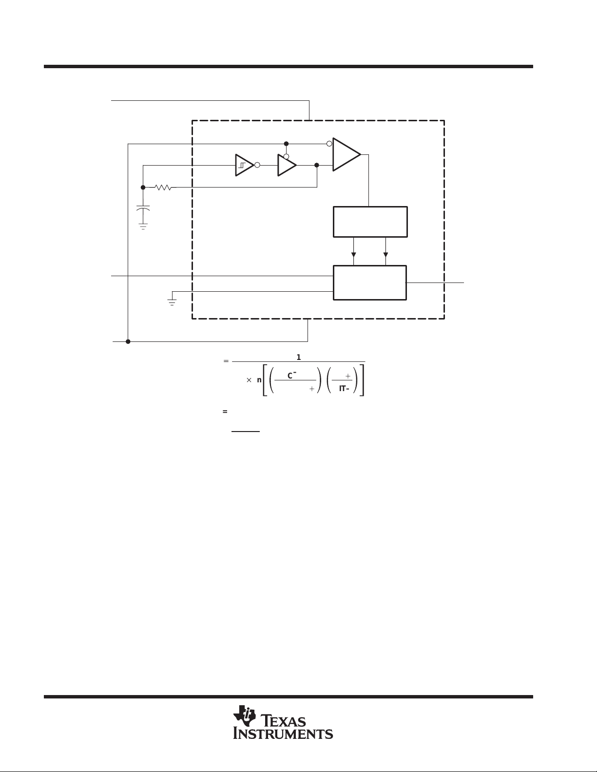
f
clock
For VCC = 10 V
f
clock
+
RC In
=
1.69 RC
Butterworth
Fourth-Order
Low-Pass Filter
V
CC–
4
1
VCC–V
ǒ
ƪ
VCC–V
IT
1
IT–
)
Ǔǒ
V
IT
)
Ǔ
ƫ
V
IT–
FILTER
OUT
Figure 5. Self-Clocking Through Schmitt-Trigger Oscillator Dual-Supply Operation
5
Filter
Output
8
POST OFFICE BOX 655303 • DALLAS, TEXAS 75265

TLC04/MF4A-50, TLC14/MF4A-100
BUTTERWORTH FOURTH-ORDER LOW-PASS
SWITCHED-CAPACITOR FILTERS
SLAS021A – NOVEMBER 1986 – REVISED MARCH 1995
APPLICATION INFORMATION
10 V
7
V
CC+
3LS
Level Shift
10 V
CMOS
CLKIN
See Note A
TTL
CLKR
FILTER IN
(see Note B)
NOTES: A. The external clock used must be of CMOS level because the clock is input to a CMOS Schmitt trigger.
B. The filter input signal should be dc-biased to midsupply or ac-coupled to the terminal.
C. AGND must be biased to midsupply.
0 V
–5 V
10 kΩ
0 V
5 VOC
0.1 µF
1 CLKIN
2 CLKR
8 FILTER IN
6 AGND
10 kΩ
See Note C
V
Nonoverlapping
Clock Generator
Butterworth
Fourth-Order
Low-Pass Filter
CC–
4
φ2φ1
FILTER
OUT
5
Figure 6. External-Clock-Driven Single-Supply Operation
POST OFFICE BOX 655303 • DALLAS, TEXAS 75265
9

TLC04/MF4A-50, TLC14/MF4A-100
BUTTERWORTH FOURTH-ORDER LOW-PASS
SWITCHED-CAPACITOR FILTERS
SLAS021A – NOVEMBER 1986 – REVISED MARCH 1995
APPLICATION INFORMATION
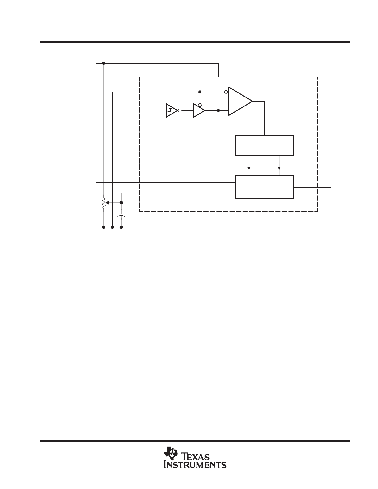
10 V
3LS
1 CLKIN
R
2 CLKR
V
CC+
7
Level Shift
C
10 kΩ
0.1 µF
8 FILTER IN
6 AGND
10 kΩ
See Note A
f
clock
For VCC = 10 V
f
clock
+
RC In
=
1.69 RC
Nonoverlapping
Clock Generator
φ1
Butterworth
Fourth-Order
Low-Pass Filter
V
CC–
4
1
VCC–V
ǒ
ƪ
VCC–V
IT
1
IT–
)
Ǔǒ
V
IT
)
Ǔ
ƫ
V
IT–
φ2
FILTER
OUT
5
10
NOTE A: AGND must be biased to midsupply.
Figure 7. Self Clocking Through Schmitt-Trigger Oscillator Single-Supply Operation
POST OFFICE BOX 655303 • DALLAS, TEXAS 75265
TLC04/MF4A-50, TLC14/MF4A-100
BUTTERWORTH FOURTH-ORDER LOW-PASS
SWITCHED-CAPACITOR FILTERS
SLAS021A – NOVEMBER 1986 – REVISED MARCH 1995
APPLICATION INFORMATION
5 V
7
V
3LS
CC+
Level Shift
Clock Input
10 kΩ
–5 V
1 CLKIN
2 CLKR
8 FILTER IN
6 AGND
0.1 µF
Figure 8. DC Offset Adjustment
V
CC–
Nonverlapping
Clock Generator
φ2φ1
Butterworth
Fourth-Order
Low-Pass Filter
4
FILTER
OUT
5
POST OFFICE BOX 655303 • DALLAS, TEXAS 75265
11

IMPORTANT NOTICE
T exas Instruments and its subsidiaries (TI) reserve the right to make changes to their products or to discontinue
any product or service without notice, and advise customers to obtain the latest version of relevant information
to verify, before placing orders, that information being relied on is current and complete. All products are sold
subject to the terms and conditions of sale supplied at the time of order acknowledgement, including those
pertaining to warranty, patent infringement, and limitation of liability.
TI warrants performance of its semiconductor products to the specifications applicable at the time of sale in
accordance with TI’s standard warranty. Testing and other quality control techniques are utilized to the extent
TI deems necessary to support this warranty . Specific testing of all parameters of each device is not necessarily
performed, except those mandated by government requirements.
CERT AIN APPLICATIONS USING SEMICONDUCTOR PRODUCTS MA Y INVOLVE POTENTIAL RISKS OF
DEATH, PERSONAL INJURY, OR SEVERE PROPERTY OR ENVIRONMENTAL DAMAGE (“CRITICAL
APPLICATIONS”). TI SEMICONDUCTOR PRODUCTS ARE NOT DESIGNED, AUTHORIZED, OR
WARRANTED TO BE SUITABLE FOR USE IN LIFE-SUPPORT DEVICES OR SYSTEMS OR OTHER
CRITICAL APPLICA TIONS. INCLUSION OF TI PRODUCTS IN SUCH APPLICATIONS IS UNDERST OOD TO
BE FULLY AT THE CUSTOMER’S RISK.
In order to minimize risks associated with the customer’s applications, adequate design and operating
safeguards must be provided by the customer to minimize inherent or procedural hazards.
TI assumes no liability for applications assistance or customer product design. TI does not warrant or represent
that any license, either express or implied, is granted under any patent right, copyright, mask work right, or other
intellectual property right of TI covering or relating to any combination, machine, or process in which such
semiconductor products or services might be or are used. TI’s publication of information regarding any third
party’s products or services does not constitute TI’s approval, warranty or endorsement thereof.
Copyright 1998, Texas Instruments Incorporated
 Loading...