

Datasheet TLC1078IDR, TLC1078ID, TLC1078CPS, TLC1078CPSR, TLC1078CP Datasheet (Texas Instruments)
...
TLC1078, TLC1078Y, TLC1079, TLC1079Y
LinCMOS µPOWER PRECISION
OPERATIONAL AMPLIFIERS
SLOS179 – FEBRUARY 1997
1
POST OFFICE BOX 655303 • DALLAS, TEXAS 75265
D
Power Dissipation as Low as 10 µW Typ Per
Amplifier
D
Operates on a Single Silver-Oxide Watch
Battery, V
DD
= 1.4 V Min
D
VIO. . . 450 µV/850 µV Max in DIP and
Small-Outline Package (TLC1078/79)
D
Input Offset Voltage Drift...0.1 µV/Month
Typ, Including the First 30 Days
D
High-impedance LinCMOS Inputs
I
IB
= 0.6 pA Typ
D
High Open-Loop Gain...800000 Typ
D
Output Drive Capability > 20 mA
D
Slew Rate...47 V/ms T yp
D
Common-Mode Input Voltage Range
Extends Below the Negative Rail
D
Output Voltage Range Includes Negative
Rail
D
On-Chip ESD-Protection Circuitry
D
Small-Outline Package Option Also
Available in Tape and Reel
description
The TLC107x operational amplifiers offer ultralow offset voltage, high gain, 1 10-kHz bandwidth,
47-V/ms slew rate, and just 150-µW power
dissipation per amplifier.
With a supply voltage of 1.4 V, common-mode
input to the negative rail, and output swing to the
negative rail, the TLC107xC is an ideal solution for
low-voltage battery-operated systems. The
20-mA output drive capability means that the
TLC107x can easily drive small resistive and large
capacitive loads when needed, while maintaining
ultra-low standby power dissipation.
Since this device is functionally compatible as well
as pin compatible with the TLC27L2/4 and
TLC27L7/9, the TLC107x easily upgrades
existing designs that can benefit from its improved
performance.
Copyright 1997, Texas Instruments Incorporated
PRODUCTION DATA information is current as of publication date.
Products conform to specifications per the terms of Texas Instruments
standard warranty. Production processing does not necessarily include
testing of all parameters.
Please be aware that an important notice concerning availability, standard warranty, and use in critical applications of
Texas Instruments semiconductor products and disclaimers thereto appears at the end of this data sheet.
LinCMOS is a trademark of Texas Instruments Incorporated.
1
2
3
4
8
7
6
5
1OUT
1IN –
1IN+
GND
V
DD
2OUT
2IN –
2IN+
3212019
910111213
4
5
6
7
8
18
17
16
15
14
NC
2OUT
NC
2IN –
NC
NC
1IN –
NC
1IN+
NC
NC
1OUT
NC
2IN +
NC
NC
NC
GND
NC
NC – No internal connection
DD
V
TLC1078
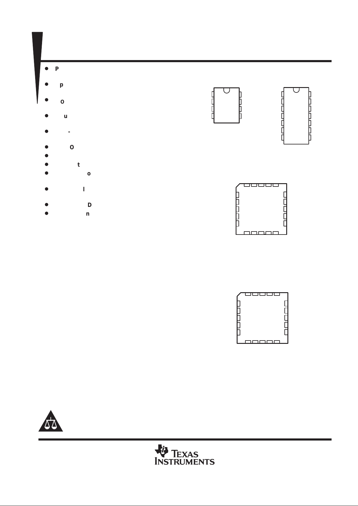
D, JG, OR P PACKAGE
(TOP VIEW)
TLC1078
FK PACKAGE
(TOP VIEW)
3212019
910111213
4
5
6
7
8
18
17
16
15
14
4IN+
NC
GND
NC
3IN+
1IN+
NC
V
DD
NC
2IN+
1IN –
1OUT
NC
3OUT
3IN –
4IN –
2IN –
2OUT
NC
4OUT
1
2
3
4
5
6
7
14
13
12
11
10
9
8
1OUT
1IN –
1IN+
V
DD
2IN+
2IN –
2OUT
4OUT
4IN –
4IN+
GND
3IN+
3IN –
3OUT
TLC1079
D, J, OR N PACKAGE
(TOP VIEW)
TLC1079
FK PACKAGE
(TOP VIEW)
TLC1078, TLC1078Y, TLC1079, TLC1079Y
LinCMOS µPOWER PRECISION
OPERATIONAL AMPLIFIERS
SLOS179 – FEBRUARY 1997
2
POST OFFICE BOX 655303 • DALLAS, TEXAS 75265
description (continued)
The TLC107x incorporates internal ESD-protection circuits that will prevent functional failures at voltages up
to 2000 V as tested under MIL-PRF-38535, Method 3015.2; however, care should be exercised when handling
these devices as exposure to ESD may result in degradation of the device parametric performance. The
TLC107x design also inhibits latch-up of the device inputs and outputs even with surge currents as large
100 mA.
The C-suffix devices are characterized for operation from 0°C to 70°C. The I-suffix devices are characterized
for operation from – 40°C to 85°C. The M-suffix devices are characterized for operation over the full military
temperature range of –55°C to 125°C. The wide range of packaging options includes small-outline and
chip-carrier versions for high-density system applications.
AVAILABLE OPTIONS
PACKAGED DEVICES
CHIP
T
A
SMALL OUTLINE
†
CHIP CARRIER CERAMIC DIP CERAMIC DIP PLASTIC DIP PLASTIC DIP
FORM
‡
(D)
(FK) (J) (JG) (N) (P)
(Y)
0°C to 70°C
TLC1078CD
TLC1079CD
— — — TLC1079CN TLC1078CP
TLC1078Y
TLC1079Y
–40°C to 85°C
TLC1078ID
TLC1079ID
— — — TLC1079IN TLC1078IP —
–55°C to 125°C
TLC1078MD
TLC1079MD
TLC1078MFK
TLC1079MFK
TLC1079MJ TLC1078MJG TLC1079MN TLC1078MP —
†
The D package is available taped and reeled. Add the suffix R to the device type (e.g., TLC1078CDR).
‡
Chip forms are tested 25°C only.
symbol (each amplifier)
OUT
–
+
IN–
IN+
TLC1078, TLC1078Y, TLC1079, TLC1079Y
LinCMOS µPOWER PRECISION
OPERATIONAL AMPLIFIERS
SLOS179 – FEBRUARY 1997
3
POST OFFICE BOX 655303 • DALLAS, TEXAS 75265
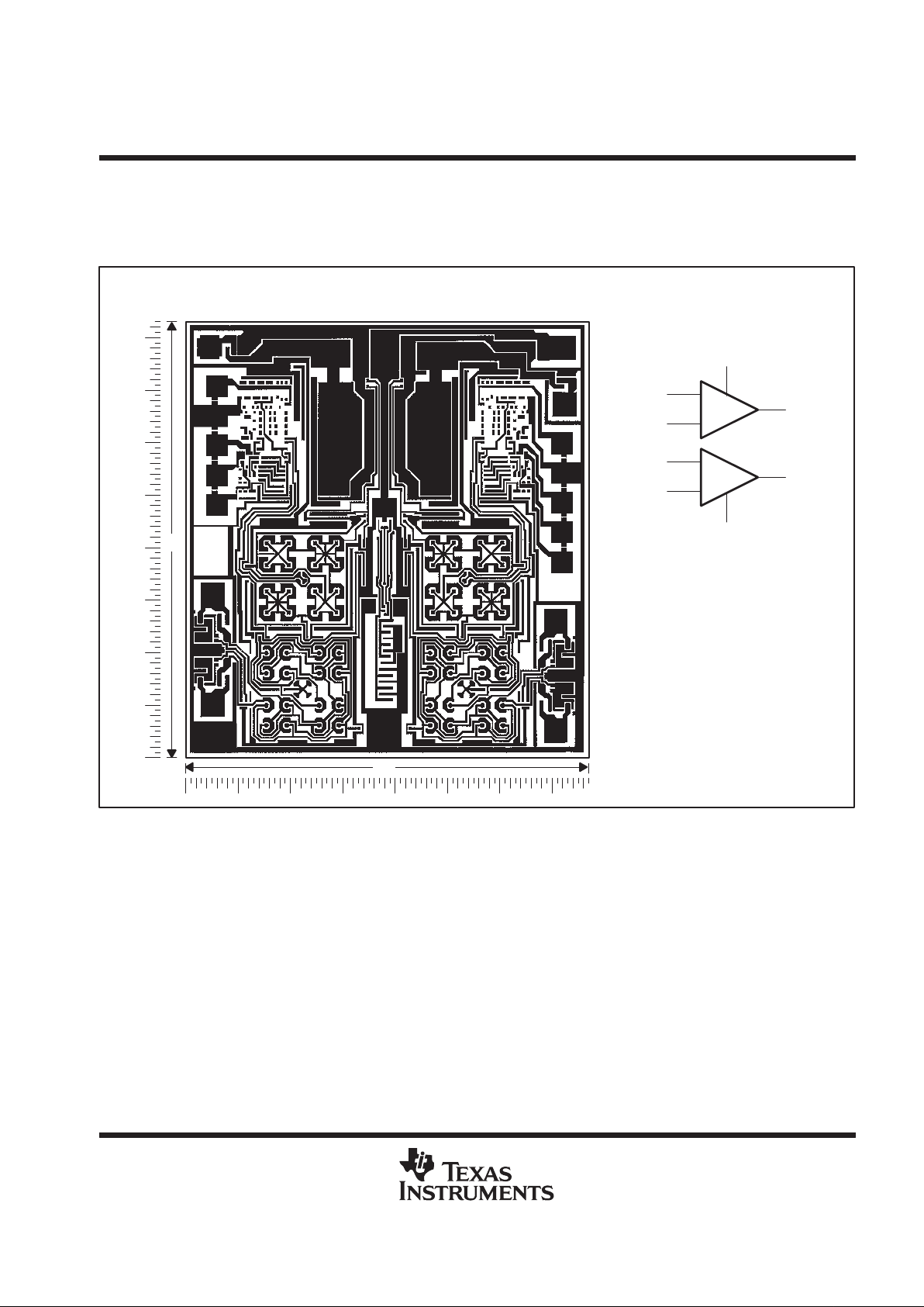
TLC1087Y chip information
This chip, when properly assembled, displays characteristics similar to the TLC1078C. Thermal compression
or ultrasonic bonding may be used on the doped-aluminum bonding pads. Chips can be mounted with
conductive epoxy or a gold-silicon preform.
BONDING PAD ASSIGNMENTS
CHIP THICKNESS: 15 MILS TYPICAL
BONDING PADS: 4 × 4 MILS MINIMUM
TJmax = 150°C
TOLERANCES ARE ±10%.
ALL DIMENSIONS ARE IN MILS.
+
–
1OUT
1IN+
1IN–
V
DD
V
DD–
/GND
(8)
(3)
(2)
(4)
+
–
2OUT
2IN+
2IN–
(5)
(6)
83
72
(1)
(5)
(4)
(3)
(2)
(6)
(7)
(8)
BONDING PAD ASSIGNMENTS
TLC1078, TLC1078Y, TLC1079, TLC1079Y
LinCMOS µPOWER PRECISION
OPERATIONAL AMPLIFIERS
SLOS179 – FEBRUARY 1997
4
POST OFFICE BOX 655303 • DALLAS, TEXAS 75265
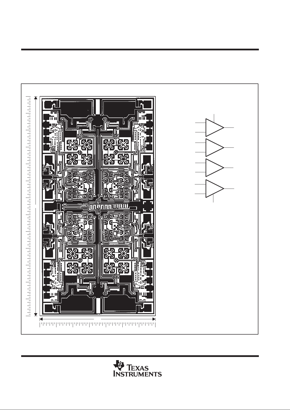
TLC1079Y chip information
This chip, when properly assembled, display characteristics similar to the TLC1079C. Thermal compression
or ultrasonic bonding may be used on the doped-aluminum bonding pads. Chips can be mounted with
conductive epoxy or a gold-silicon preform.
BONDING PAD ASSIGNMENTS
+
–
1OUT
1IN+
1IN–
V
DD
(4)
(6)
(3)
(2)
(5)
(1)
2IN+
2IN–
2OUT
(11)
V
DD–
/GND
+
–
3OUT
3IN+
3IN–
(13)
(10)
(9)
(12)
(8)
–
+
(14)
4OUT
4IN+
4IN–
+
–
(7)
CHIP THICKNESS: 15 MILS TYPICAL
BONDING PADS: 4 × 4 MILS MINIMUM
TJmax = 150°C
TOLERANCES ARE ±10%.
ALL DIMENSIONS ARE IN MILS.
PIN (11) IS INTERNALLY CONNECTED
TO BACKSIDE OF CHIP.
130
70
(1)
(2)
(3)
(4)
(5)
(6)
(7)
(8)
(9)
(10)
(11)
(12)
(13)
(14)
TLC1078, TLC1078Y, TLC1079, TLC1079Y
LinCMOS µPOWER PRECISION
OPERATIONAL AMPLIFIERS
SLOS179 – FEBRUARY 1997
5
POST OFFICE BOX 655303 • DALLAS, TEXAS 75265
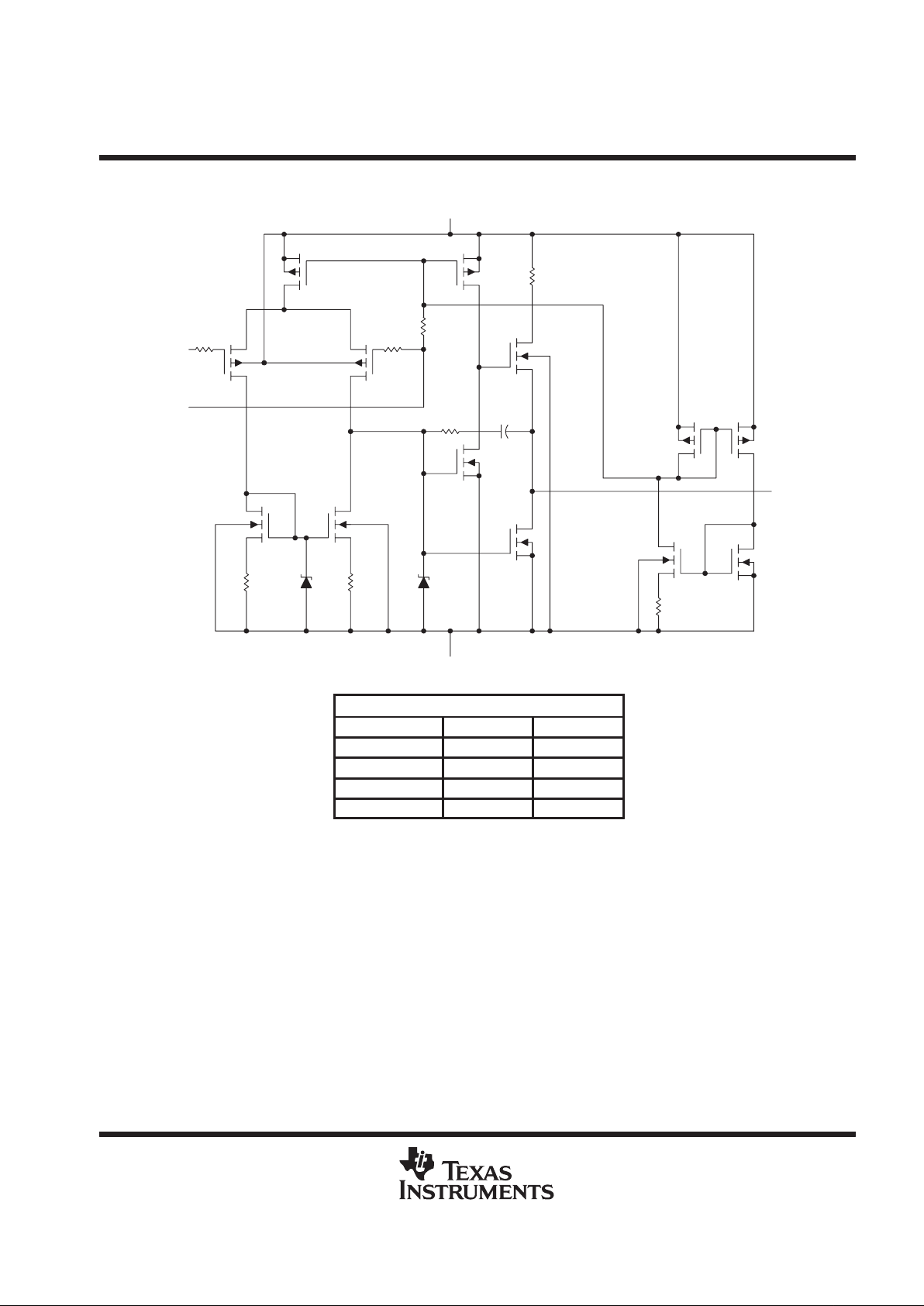
equivalent schematic (each amplifier)
R2 D1
R3
Q4Q2
Q1
R1
IN–
IN+
R4
Q5
R5
Q3 Q6
V
DD
GND
Q7
Q9
D2
C1
R6
R7
Q10
Q13
OUT
Q11
Q12
Q8
ACTUAL DEVICE COMPONENT COUNT
COMPONENT TLC1078 TLC1079
Transistors 38 76
Resistors 16 32
Diodes 12 24
Capacitors 2 4
TLC1078, TLC1078Y, TLC1079, TLC1079Y
LinCMOS µPOWER PRECISION
OPERATIONAL AMPLIFIERS
SLOS179 – FEBRUARY 1997
6
POST OFFICE BOX 655303 • DALLAS, TEXAS 75265
absolute maximum ratings over operating free-air temperature range (unless otherwise noted)
†
Supply voltage, V
DD
(see Note 1) 18 V. . . . . . . . . . . . . . . . . . . . . . . . . . . . . . . . . . . . . . . . . . . . . . . . . . . . . . . . . . . .
Differential input voltage, V
ID
(see Note 2) ±V
DD
. . . . . . . . . . . . . . . . . . . . . . . . . . . . . . . . . . . . . . . . . . . . . . . . . . .
Input voltage range, V
I
(any input) –0.3 V to V
DD
. . . . . . . . . . . . . . . . . . . . . . . . . . . . . . . . . . . . . . . . . . . . . . . . . . .
Input current, I
I
(each input) ± 5 mA. . . . . . . . . . . . . . . . . . . . . . . . . . . . . . . . . . . . . . . . . . . . . . . . . . . . . . . . . . . . . . .
Output current, I
O
(each output) ± 30 mA. . . . . . . . . . . . . . . . . . . . . . . . . . . . . . . . . . . . . . . . . . . . . . . . . . . . . . . . . .
Total current into V
DD
(see Note 3) 45 mA. . . . . . . . . . . . . . . . . . . . . . . . . . . . . . . . . . . . . . . . . . . . . . . . . . . . . . . . .
Duration of short-circuit at (or below) T
A
= 25°C (see Note 3) unlimited. . . . . . . . . . . . . . . . . . . . . . . . . . . . . . . .
Continuous total power dissipation see Dissipation Rating Table. . . . . . . . . . . . . . . . . . . . . . . . . . . . . . . . . . . . . .
Operating free-air temperature range, T
A
: C suffix 0°C to 70°C. . . . . . . . . . . . . . . . . . . . . . . . . . . . . . . . . . . . . . .
I suffix –40°C to 85°C. . . . . . . . . . . . . . . . . . . . . . . . . . . . . . . . . . . . . .
M suffix –55°C to 125°C. . . . . . . . . . . . . . . . . . . . . . . . . . . . . . . . . . . .
Storage temperature range –65°C to 150°C. . . . . . . . . . . . . . . . . . . . . . . . . . . . . . . . . . . . . . . . . . . . . . . . . . . . . . . .
Case temperature for 60 seconds: FK package 260°C. . . . . . . . . . . . . . . . . . . . . . . . . . . . . . . . . . . . . . . . . . . . . .
Lead temperature 1,6 mm (1/16 inch) from case for 10 seconds: D or P package 260°C. . . . . . . . . . . . . . . . .
Lead temperature 1,6 mm (1/16 inch) from case for 60 seconds: JG package 300°C. . . . . . . . . . . . . . . . . . . .
†
Stresses beyond those listed under “absolute maximum ratings” may cause permanent damage to the device. These are stress ratings only, and
functional operation of the device at these or any other conditions beyond those indicated under “recommended operating conditions” is not
implied. Exposure to absolute-maximum-rated conditions for extended periods may affect device reliability.
NOTES: 1. All voltage values, except differential voltages, are with respect to network ground.
2. Differential voltages are at IN+ with respect to IN–.
3. The output may be shorted to either supply. Temperature and/or supply voltages must be limited to ensure that the maximum
dissipation ratings are not exceeded.
DISSIPATION RATING TABLE
PACKAGE
TA ≤ 25°C
POWER RATING
DERATING FACTOR
ABOVE TA = 25°C
TA = 70°C
POWER RATING
TA = 85°C
POWER RATING
TA = 125°C
POWER RATING
D–8 725 mW 5.8 mW/°C 464 mW 377 mW 145 mW
D–14 950 mW 7.6 mW/°C 608 mW 494 mW 190 mW
FK 1375 mW 11.0 mW/°C 880 mW 715 mW 275 mW
J 1375 mW 11.0 mW/°C 880 mW 715 mW 275 mW
JG 1050 mW 8.4 mW/°C 672 mW 546 mW 210 mW
N 1150 mW 9.2 mW/°C 736 mW 598 mW 230 mW
P 1000 mW 8.0 mW/°C 640 mW 520 mW 200 mW
recommended operating conditions
C SUFFIX I SUFFIX M SUFFIX
MIN MAX MIN MAX MIN MAX
UNIT
Supply voltage, V
DD
1.4 16 3 16 4 16 V
p
VDD = 5 V –0.2 4 –0.2 4 0 4
Common-mode input voltage, V
IC
VDD = 10 V –0.2 9 –0.2 9 0 9
V
Operating free-air temperature, T
A
0 70 –40 85 –55 125 °C
TLC1078, TLC1078Y, TLC1079, TLC1079Y
LinCMOS µPOWER PRECISION
OPERATIONAL AMPLIFIERS
SLOS179 – FEBRUARY 1997
7
POST OFFICE BOX 655303 • DALLAS, TEXAS 75265
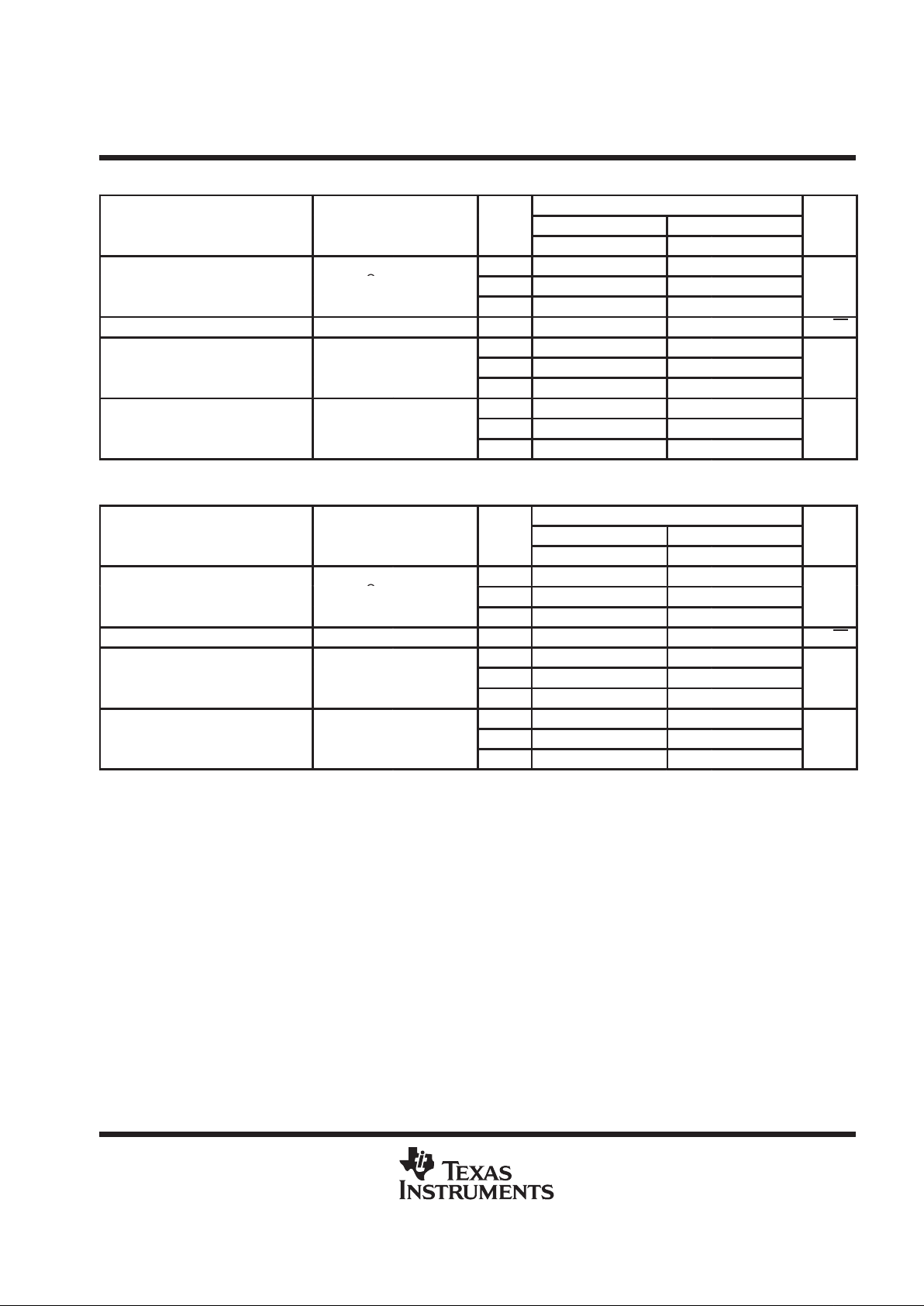
electrical characteristics at specified free-air temperature
TLC1078C
PARAMETER
TEST
T
A
†
VDD = 5 V VDD = 10 V
UNIT
CONDITIONS
A
MIN TYP MAX MIN TYP MAX
p
=
25°C 160 450 180 600
VIOInput offset voltage
V
O
= 1.4 V,
RS = 50 Ω,
Full range 800 950
µ
V
α
VIO
Temperature coefficient of input
offset voltage
VIC = 0,
RI = 1 MΩ
25°C to 70°C 1.1 1 µV/°C
p
25°C 0.1 0.1
p
IIOInput offset current (see Note 4)
V
= V
/ 2,
70°C 7 300 7 300
pA
p
ODD
,
VIC = VDD/ 2
25°C 0.6 0.7
p
IIBInput bias current (see Note 4)
70°C 40 600 50 600
pA
Common-mode input voltage
25°C
–0.2
to 4
–0.3
to 4.2
–0.2
to 9
–0.3
to 9.2
V
V
ICR
g
range (see Note 5)
Full range
–0.2
to 3.5
–0.2
to 8.5
V
25°C 3.2 4.1 8.2 8.9
V
OH
High-level output voltage
VID = 100 mV ,
0°C 3.2 4.1 8.2 8.9
V
RL= 1 MΩ
70°C 3.2 4.2 8.2 8.9
25°C 0 25 0 25
V
OL
Low-level output voltage
VID = –100 mV ,
0°C 0 25 0 25
mV
I
OL
=
0
70°C 0 25 0 25
25°C 250 525 500 850
A
VD
Large-signal differential voltage
p
RL= 1 MΩ,
0°C 250 680 500 1010
V/mV
am lification
See Note 6
70°C 200 380 350 660
25°C 70 95 75 97
CMRR Common-mode rejection ratio VIC = V
ICR
min
0°C 70 95 75 97
dB
70°C 70 95 75 97
25°C 75 98 75 98
k
SVR
Supply-voltage rejection ratio
VO = 1.4 V
0°C 75 98 75 98
dB
(∆VDD/∆VIO)
70°C 75 98 75 98
V
= V
/ 2
,
25°C 20 34 29 46
I
DD
Supply current (two amplifiers)
V
O
VDD/ 2,
VIC = VDD/ 2,
0°C 24 42 36 66
µA
No load
70°C 16 28 22 40
†
Full range is 0°C to 70°C.
NOTES: 4. The typical values of input bias current and input offset current below 5 pA were determined mathematically .
5. This range also applies to each input individually.
6. At VDD = 5 V. VO = 0.25 V to 2 V; at VDD = 10 V, VO = 1 V to 6 V.
TLC1078, TLC1078Y, TLC1079, TLC1079Y
LinCMOS µPOWER PRECISION
OPERATIONAL AMPLIFIERS
SLOS179 – FEBRUARY 1997
8
POST OFFICE BOX 655303 • DALLAS, TEXAS 75265
electrical characteristics at specified free-air temperature
TLC1079C
PARAMETER TEST CONDITIONS T
A
†
VDD = 5 V VDD = 10 V
UNIT
MIN TYP MAX MIN TYP MAX
p
25°C 190 850 200 1150
VIOInput offset voltage
VO = 1.4 V, VIC = 0,
Full range
1200 1500
µ
V
α
VIO
T emperature coef ficient of
input offset voltage
RS = 50 Ω, RI = 1 MΩ
25°C to
70°C
1.1 1 µV/°C
Input offset current
25°C 0.1 0.1
p
I
IO
(see Note 4)
V
= V
/ 2,
70°C 7 300 7 300
pA
Input bias current
ODD
,
VIC = VDD/ 2
25°C 0.6 0.7
p
I
IB
(see Note 4)
70°C 40 600 50 600
pA
Common mode input
25°C
–0.2
to 4
–0.3
to 4.2
–0.2
to 9
–0.3
to 9.2
V
V
ICR
voltage range (see Note 5)
Full range
–0.2
to 3.5
–0.2
to 8.5
V
25°C 3.2 4.1 8.2 8.9
V
OH
High-level output voltage
VID = 100 mV ,
0°C 3.2 4.1 8.2 8.9
V
R
L
= 1
MΩ
70°C 3.2 4.2 8.2 8.9
25°C 0 25 0 25
V
OL
Low-level output voltage
VID = –100 mV ,
0°C 0 25 0 25
mV
I
OL
=
0
70°C 0 25 0 25
25°C 250 525 500 850
A
VD
Large-signal differential
p
RL = 1 MΩ, See Note 6
0°C 250 700 500 1010
V/mV
voltage am lification
70°C 200 380 350 660
25°C 70 95 75 97
CMRR
Common mode rejection
VIC = V
ICR
min
0°C 70 95 75 97
dB
ratio
70°C 70 95 75 97
25°C 75 98 75 98
k
SVR
Supply-voltage rejection
VDD = 5 V to 10 V,
0°C 75 98 75 98
dB
ratio (∆VDD/∆VIO)
V
O
= 1.4
V
70°C 75 98 75 98
25°C 40 68 57 92
I
DD
S
upply current (four
p
V
O
=
VDD/ 2
,
=
0°C 48 84 72 132
µA
am lifiers)
V
IC
=
VDD/ 2
, No
load
70°C 31 56 44 80
†
Full range is 0°C to 70°C.
NOTES: 4. The typical values of input bias current and input offset current below 5 pA were determined mathematically.
5. This range also applies to each input individually.
6. At VDD = 5 V, VO = 0.25 V to 2 V; at VDD = 10 V, VO = 1 V to 6 V.
TLC1078, TLC1078Y, TLC1079, TLC1079Y
LinCMOS µPOWER PRECISION
OPERATIONAL AMPLIFIERS
SLOS179 – FEBRUARY 1997
9
POST OFFICE BOX 655303 • DALLAS, TEXAS 75265
operating characteristics at specified free-air temperature
TLC1078C
PARAMETER TEST CONDITIONS T
A
VDD = 5 V VDD = 10 V
UNIT
MIN TYP MAX MIN TYP MAX
25°C 32 47
SR Slew rate at unity gain
RL = 1 MΩ,
CL = 20 pF,
0°C 35 51
V/ms
V
I(PP)
= 1 V,
See Figure 1
70°C 27 38
VnEquivalent input noise voltage f = 1 kHz, RS = 20 Ω 25°C 68 68 nV/√Hz
25°C 85 110
B1Unity-gain bandwidth CL = 20 pF, See Figure 2
0°C
100 125
kHz
70°C 65 90
25°C 34° 38°
φmPhase margin at unity gain CL = 20 pF, See Figure 2
0°C
36° 40°
70°C 30° 34°
operating characteristics at specified free-air temperature
TLC1079C
PARAMETER TEST CONDITIONS T
A
VDD = 5 V VDD = 10 V
UNIT
MIN TYP MAX MIN TYP MAX
25°C 32 47
SR Slew rate at unity gain
RL = 1 MΩ,
CL = 20 pF,
0°C 35 51
V/ms
V
I(PP)
= 1 V,
See Figure 1
70°C 27 38
VnEquivalent input noise voltage f = 1 kHz, RS = 20 Ω 25°C 68 68 nV/√Hz
25°C 85 110
B1Unity-gain bandwidth CL = 20 pF, See Figure 2
0°C
100 125
kHz
70°C 65 90
25°C 34° 38°
φmPhase margin at unity gain CL = 20 pF, See Figure 2
0°C
36° 40°
70°C 30° 34°
TLC1078, TLC1078Y, TLC1079, TLC1079Y
LinCMOS µPOWER PRECISION
OPERATIONAL AMPLIFIERS
SLOS179 – FEBRUARY 1997
10
POST OFFICE BOX 655303 • DALLAS, TEXAS 75265
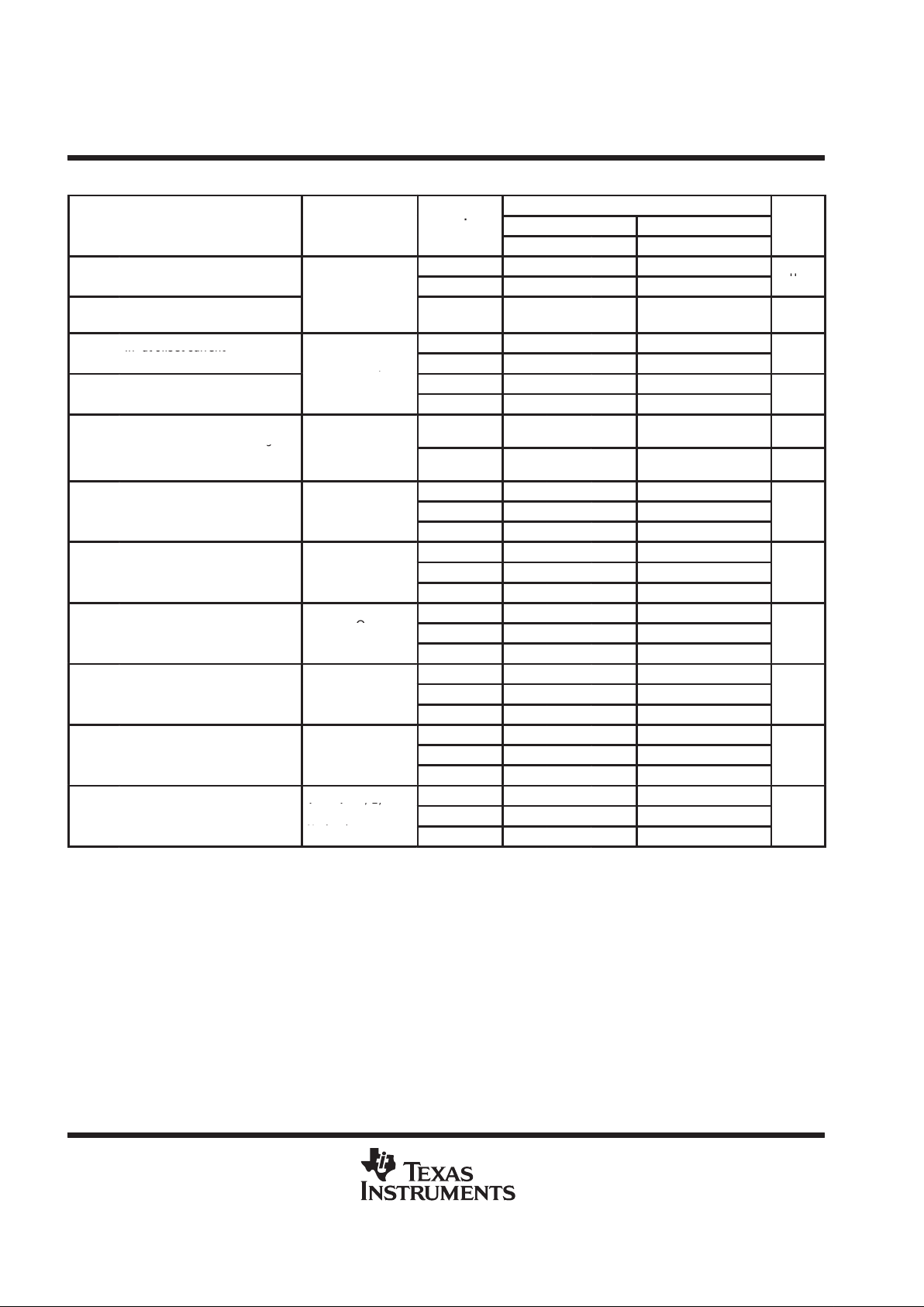
electrical characteristics at specified free-air temperature
TLC1078I
PARAMETER
TEST
T
A
†
VDD = 5 V VDD = 10 V
UNIT
CONDITIONS
A
MIN TYP MAX MIN TYP MAX
p
25°C 160 450 180 600
VIOInput offset voltage
VO = 1.4 V,
Full range 950 1100
µ
V
α
VIO
Temperature coefficient of input
offset voltage
R
S
= 50 Ω,
VIC = 0, RI = 1 MΩ
25°C to 85°C 1.1 1 µV/°C
Input offset current
25°C 0.1 0.1
p
I
IO
In ut offset current
(see Note 4)
V
= V
/ 2,
85°C 24 1000 26 1000
pA
p
ODD
,
VIC = VDD/ 2
25°C 0.6 0.7
p
IIBInput bias current (see Note 4)
85°C 200 2000 220 2000
pA
Common-mode input voltage
25°C
–0.2
to 4
–0.3
to 4.2
–0.2
to 9
–0.3
to 9.2
V
V
ICR
g
range (see Note 5)
Full range
–0.2
to 3.5
–0.2
to 8.5
V
25°C 3.2 4.1 8.2 8.9
V
OH
High-level output voltage
VID = 100 mV ,
–40°C 3.2 4.1 8.2 8.9
V
R
L
= 1
MΩ
85°C 3.2 4.2 8.2 8.9
25°C 0 25 0 25
V
OL
Low-level output voltage
VID = –100 mV ,
–40°C 0 25 0 25
mV
I
OL
=
0
85°C 0 25 0 25
25°C 250 525 500 850
A
VD
Large-signal differential voltagepRL = 1 MΩ,
–40°C 250 900 500 1550
V/mV
am lification
See Note 6
85°C 150 300 250 585
25°C 70 95 75 97
CMRR Common-mode rejection ratio VIC = V
ICR
min
–40°C 70 95 75 97
dB
85°C 70 95 75 97
25°C 75 98 75 98
k
SVR
Supply-voltage rejection ratio
VO = 1.4 V
–40°C 75 98 75 98
dB
(∆VDD/∆VIO)
85°C 75 98 75 98
V
= V
/ 2
,
25°C 20 34 29 46
I
DD
Supply current (two amplifiers)
V
O
VDD/ 2,
VIC = VDD/ 2,
–40°C 31 54 50 86
µA
No load
85°C 15 26 20 36
†
Full range is –40°C to 80°C.
NOTES: 4. The typical values of input bias current and input offset current below 5 pA were determined mathematically.
5. This range also applies to each input individually.
6. At VDD = 5 V, VO = 0.25 V to 2 V; at VDD = 10 V, VO = 1 V to 6 V.

TLC1078, TLC1078Y, TLC1079, TLC1079Y
LinCMOS µPOWER PRECISION
OPERATIONAL AMPLIFIERS
SLOS179 – FEBRUARY 1997
11
POST OFFICE BOX 655303 • DALLAS, TEXAS 75265
electrical characteristics at specified free-air temperature
TLC1079I
PARAMETER TEST CONDITIONS T
A
†
VDD = 5 V VDD = 10 V
UNIT
MIN TYP MAX MIN TYP MAX
p
25°C 190 850 200 1150
VIOInput offset voltage
VO = 1.4 V, VIC = 0,
Full range
1350 1650
µ
V
α
VIO
T emperature coef ficient
of input offset voltage
RS = 50 Ω, RI = 1 MΩ
25°C to
85°C
1.1 1 µV/°C
Input offset current
25°C 0.1 0.1
p
I
IO
(see Note 4)
V
= V
/ 2,
85°C 24 1000 26 1000
pA
Input bias current
ODD
,
VIC = VDD/ 2
25°C 0.6 0.7
p
I
IB
(see Note 4)
85°C 200 2000 220 2000
pA
Common-mode input
25°C
–0.2
to 4
–0.3
to 4.2
–0.2
to 9
–0.3
to 9.2
V
V
ICR
voltage range
(see Note 5)
Full range
–0.2
to 3.5
–0.2
to 8.5
V
25°C 3.2 4.1 8.2 8.9
V
OH
High-level output voltage
VID = 100 mV ,
–40°C 3.2 4.1 8.2 8.9
V
R
L
= 1
MΩ
85°C 3.2 4.2 8.2 8.9
25°C 0 25 0 25
V
OL
Low-level output voltage
VID = –100 mV ,
–40°C 0 25 0 25
mV
I
OL
=
0
85°C 0 25 0 25
25°C 250 525 500 850
A
VD
Large-signal differential
p
RL = 1 MΩ, See Note 6
–40°C
250 900 500 1550
V/mV
voltage am lification
85°C 150 330 250 585
25°C 70 95 75 97
CMRR
Common-mode
VIC = V
ICR
min
–40°C 70 95 75 97
dB
rejection ratio
85°C 70 95 75 97
25°C 75 98 75 98
k
SVR
Supply-voltage rejection
VDD = 5 V to 10 V,
–40°C 75 98 75 98
dB
ratio (∆VDD/∆VIO)
V
O
= 1.4
V
85°C 75 98 75 98
25°C 40 68 57 92
I
DD
S
upply curren
t
p
V
O
=
VDD/ 2
,
–40°C 62 108 98 172
µA
(four am lifiers)
V
IC
=
VDD/ 2
, No
load
85°C 29 52 40 72
†
Full range is –40°C to 85°C.
NOTES: 4. The typical values of input bias current and input offset current below 5 pA were determined mathematically.
5. This range also applies to each input individually.
6. At VDD = 5 V, VO = 0.25 V to 2 V; at VDD = 10 V, VO = 1 V to 6 V.

TLC1078, TLC1078Y, TLC1079, TLC1079Y
LinCMOS µPOWER PRECISION
OPERATIONAL AMPLIFIERS
SLOS179 – FEBRUARY 1997
12
POST OFFICE BOX 655303 • DALLAS, TEXAS 75265
operating characteristics at specified free-air temperature
TLC1078I
PARAMETER TEST CONDITIONS T
A
VDD = 5 V VDD = 10 V
UNIT
MIN TYP MAX MIN TYP MAX
25°C 32 47
SR Slew rate at unity gain
RL = 1 MΩ,
CL = 20 pF,
–40°C 39 59
V/ms
V
I(PP)
= 1 V,
See Figure 1
85°C 25 34
VnEquivalent input noise voltage f = 1 kHz, RS = 20 Ω 25°C 68 68
nV/√Hz
25°C 85 110
B1Unity-gain bandwidth CL = 20 pF, See Figure 2
–40°C 130 155
kHz
85°C 55 80
25°C 34° 38°
φmPhase margin at unity gain CL = 20 pF, See Figure 2
–40°C
38° 40°
85°C 28° 32°
operating characteristics at specified free-air temperature
TLC1079I
PARAMETER TEST CONDITIONS T
A
VDD = 5 V VDD = 10 V
UNIT
MIN TYP MAX MIN TYP MAX
25°C 32 47
SR Slew rate at unity gain
RL = 1 MΩ,
CL = 20 pF,
–40°C 39 59
V/ms
V
I(PP)
= 1 V,
See Figure 1
85°C 25 34
VnEquivalent input noise voltage f = 1 kHz, RS = 20 Ω 25°C 68 68 nV/√Hz
25°C 85 110
B1Unity-gain bandwidth CL = 20 pF, See Figure 2
–40°C 130 155
kHz
85°C 55 80
25°C 34° 38°
φmPhase margin at unity gain CL = 20 pF, See Figure 2
–40°C
38° 42°
85°C 28° 32°

TLC1078, TLC1078Y, TLC1079, TLC1079Y
LinCMOS µPOWER PRECISION
OPERATIONAL AMPLIFIERS
SLOS179 – FEBRUARY 1997
13
POST OFFICE BOX 655303 • DALLAS, TEXAS 75265
electrical characteristics at specified operating free-air temperature
TLC1078M
PARAMETER
TEST
T
A
†
VDD = 5 V VDD = 10 V
UNIT
CONDITIONS
A
MIN TYP MAX MIN TYP MAX
p
=
25°C 160 450 180 600
VIOInput offset voltage
V
O
= 1.4 V,
VIC = 0,
Full range 1250 1400
µ
V
α
VIO
T emperature coef ficient of
input offset voltage
RS = 50 Ω,
RL = 1 MΩ
25°C to 125°C 1.4 1.4 µV/°C
Input offset current
25°C 0.1 0.1 pA
I
IO
(see Note 4)
V
= V
/ 2,
125°C 1.4 15 1.8 15 nA
Input bias current
ODD
,
VIC = VDD/ 2
25°C 0.6 0.7 pA
I
IB
In ut bias current
(see Note 4)
125°C 9 35 10 35 nA
Common-mode input
25°C
0
to 4
–0.3
to 4.2
0
to 9
–0.3
to 9.2
V
V
ICR
Common mode in ut
voltage range (see Note 5)
Full range
0
to 3.5
0
to 8.5
V
25°C 3.2 4.1 8.2 8.9
V
OH
High-level output voltage
VID = 100 mV ,
–55°C 3.2 4.1 8.2 8.8
V
RL= 1 MΩ
125°C 3.2 4.2 8.2 9
25°C 0 25 0 25
V
OL
Low-level output voltage
VID = –100 mV ,
–55°C 0 25 0 25
mV
I
OL
=
0
125°C 0 25 0 25
25°C 250 525 500 850
A
VD
Large-signal differential
p
RL= 1 MΩ ,
–55°C 250 950 500 1750
V/mV
voltage am lification
See Note 6
125°C 35 200 75 380
25°C 70 95 75 97
CMRR Common-mode rejection ratio VIC = V
ICR
min
–55°C 70 95 75 97
dB
125°C 70 85 75 91
25°C 75 98 75 98
k
SVR
Supply-voltage rejection ratio
VO = 1.4 V
–55°C 70 98 70 98
dB
(∆VDD/∆VIO)
125°C 70 98 70 98
V
= V
/ 2,
25°C 20 34 29 46
I
DD
Supply current (two
amplifiers
)
V
O
VDD/ 2,
VIC = VDD/ 2,
–55°C 35 60 56 96
µA
am lifiers)
No load
125°C 14 24 18 30
†
Full range is –55°C to 125°C.
NOTES: 4. The typical values of input bias current and input offset current below 5 pA were determined mathematically.
5. This range also applies to each input individually.
6. At VDD = 5 V, VO = 0.25 V to 2 V; at VDD = 10 V, VO = 1 V to 6 V.

TLC1078, TLC1078Y, TLC1079, TLC1079Y
LinCMOS µPOWER PRECISION
OPERATIONAL AMPLIFIERS
SLOS179 – FEBRUARY 1997
14
POST OFFICE BOX 655303 • DALLAS, TEXAS 75265
electrical characteristics at specified free-air temperature
TLC1079M
PARAMETER TEST CONDITIONS T
A
†
VDD = 5 V VDD = 10 V
UNIT
MIN TYP MAX MIN TYP MAX
p
25°C 190 850 200 1150
VIOInput offset voltage
VO = 1.4 V, VIC = 0,
Full range
1600 1900
µ
V
α
VIO
T emperature coef ficient of
input offset voltage
RS = 50 Ω, RI = 1 MΩ
25°C to
125°C
1.4 1.4 µV/°C
Input offset current
25°C 0.1 0.1 pA
I
IO
(see Note 4)
V
= V
/ 2,
125°C 1.4 15 1.8 15 nA
Input bias current
ODD
,
VIC = VDD/ 2
25°C 0.6 0.7 pA
I
IB
(see Note 4)
125°C 9 35 10 35 nA
Common mode input
25°C
0
to 4
–0.3
to 4.2
0
to 9
–0.3
to 9.2
V
V
ICR
voltage range (see Note 5)
Full range
0
to 3.5
0
to 8.5
V
25°C 3.2 4.1 8.2 8.9
V
OH
High-level output voltage
VID = 100 mV ,
–55°C 3.2 4.1 8.2 8.9
V
R
L
= 1
MΩ
125°C 3.2 4.2 8.2 9
25°C 0 25 0 25
V
OL
Low-level output voltage
VID = –100 mV ,
–55°C 0 25 0 25
mV
I
OL
=
0
125°C 0 25 0 25
25°C 250 525 500 850
A
VD
Large-signal differential
p
RL = 1 MΩ, See Note 6
–55°C 250 950 500 1750
V/mV
voltage am lification
125°C 35 200 75 380
25°C 70 95 75 97
CMRR
Common-mode rejection
VIC = V
ICR
min
–55°C 70 95 75 97
dB
ratio
125°C 70 85 75 91
25°C 75 98 75 98
k
SVR
Supply voltage rejection
VDD = 5 V to 10 V,
–55°C 70 98 70 98
dB
ratio (∆VDD/∆VIO)
V
O
= 1.4
V
125°C 70 98 70 98
25°C 40 68 57 92
I
DD
S
upply curren
t
p
V
O
=
VDD/ 2
,
=
–55°C 69 120 111 192
µA
(four am lifiers)
V
IC
=
VDD/ 2
, No
load
125°C 27 48 35 60
†
Full range is –55°C to 125°C.
NOTES: 4. The typical values of input bias current and input offset current below 5 pA were determined mathematically.
5. This range also applies to each input individually.
6. At VDD = 5 V, VO = 0.25 V to 2 V; at VDD = 10 V, VO = 1 V to 6 V.

TLC1078, TLC1078Y, TLC1079, TLC1079Y
LinCMOS µPOWER PRECISION
OPERATIONAL AMPLIFIERS
SLOS179 – FEBRUARY 1997
15
POST OFFICE BOX 655303 • DALLAS, TEXAS 75265
operating characteristics at specified free-air temperature
TLC1078M
PARAMETER TEST CONDITIONS T
A
VDD = 5 V VDD = 10 V
UNIT
MIN TYP MAX MIN TYP MAX
25°C 32 47
SR Slew rate at unity gain
RL = 1 MΩ,
CL = 20 pF,
–55°C 41 63
V/ms
V
I(PP)
= 1 V,
See Figure 1
125°C 20 27
VnEquivalent input noise voltage f = 1 kHz, RS = 20 Ω 25°C 68 68 nV/√Hz
25°C 85 110
B1Unity-gain bandwidth CL = 20 pF, See Figure 2
–55°C 140 165
kHz
125°C 45 70
25°C 34° 38°
φmPhase margin at unity gain CL = 20 pF, See Figure 2
–55°C
39° 43°
125°C 25° 29°
operating characteristics at specified free-air temperature
TLC1079M
PARAMETER TEST CONDITIONS T
A
VDD = 5 V VDD = 10 V
UNIT
MIN TYP MAX MIN TYP MAX
25°C 32 47
SR Slew rate at unity gain
RL = 1 MΩ,
CL = 20 pF,
–55°C 41 63
V/ms
V
I(PP)
= 1 V,
See Figure 1
125°C 20 27
VnEquivalent input noise voltage f = 1 kHz, RS = 20 Ω 25°C 68 68 nV/√Hz
25°C 85 110
p
–55°C 140 165
B1Unity-gain bandwidth
C
L
=
20 pF
,
See Figure 2
125°C 45 70
25°C 34° 38°
kH
z
p
–55°C 39° 43°
φmPhase margin at unity gain
C
L
= 20 pF,
See Figure 2
125°C 25° 29°

TLC1078, TLC1078Y, TLC1079, TLC1079Y
LinCMOS µPOWER PRECISION
OPERATIONAL AMPLIFIERS
SLOS179 – FEBRUARY 1997
16
POST OFFICE BOX 655303 • DALLAS, TEXAS 75265
PARAMETER MEASUREMENT INFORMATION
–
+
R
L
V
DD
V
O
V
I
–
+
V
DD/2
10 kΩ
V
DD
C
L
V
O
100 Ω
V
I
(see Note A)
NOTE A: CL includes fixture capacitance.
Figure 1. Slew-Rate Test Circuit
Figure 2. Unity-Gain Bandwidth and
Phase-Margin Test Circuit
C
L
(see Note A)

TLC1078, TLC1078Y, TLC1079, TLC1079Y
LinCMOS µPOWER PRECISION
OPERATIONAL AMPLIFIERS
SLOS179 – FEBRUARY 1997
17
POST OFFICE BOX 655303 • DALLAS, TEXAS 75265
TYPICAL CHARACTERISTICS
Table of Graphs
FIGURE
α
VIO
Temperature coefficient of input offset voltage Distribution 3 – 6
I
IB
Input bias current vs Free-air temperature 7
I
IO
Input offset current vs Free-air temperature 7
V
IC
Common-mode input voltage vs Supply voltage 8
V
OH
High-level output voltage
vs High-level output current
vs Supply voltage
vs Free-air temperature
9, 10
11
12
V
OL
Low-level output voltage
vs Common-mode input voltage
vs Differential input voltage
vs Free-air temperature
vs Low-level output current
13, 14
15
16
17, 18
A
VD
Large-signal differential voltage amplification
vs Supply voltage
vs Free-air temperature
vs Frequency
19
20
21, 22
V
OM
Maximum peak output voltage vs Frequency 23
I
DD
Supply current
vs Supply voltage
vs Free-air temperature
24
25
SR Slew rate
vs Supply voltage
vs Free-air temperature
26
27
Normalized slew rate vs Free-air temperature 28
V
n
Equivalent input noise voltage vs Frequency 29
B
1
Unity-gain bandwidth
vs Supply voltage
vs Free-air temperature
30
31
φ
m
Phase margin
vs Supply voltage
vs Free-air temperature
vs Capacitance load
32
33
34
Phase shift vs Frequency 21, 22

TLC1078, TLC1078Y, TLC1079, TLC1079Y
LinCMOS µPOWER PRECISION
OPERATIONAL AMPLIFIERS
SLOS179 – FEBRUARY 1997
18
POST OFFICE BOX 655303 • DALLAS, TEXAS 75265
TYPICAL CHARACTERISTICS
Figure 3
–10
0
Percentage of Amplifiers – %
α
VIO
– Temperature Coefficient – µV/°C
10
70
–8 –6 –4 –2 0 2 4 6 8
10
20
30
40
50
60
356 Amplifiers Tested From 8 Water Lots
VDD = 5 V
TA = 25°C to 125°C
P Package
Outliers:
(1) 19.2 µV/°C
(1) 12.1 µV/°C
DISTRIBUTION OF TLC1078
INPUT OFFSET VOLTAGE
TEMPERATURE COEFFICIENT
Figure 4
VDD = 10 V
TA = 25°C to 125°C
P Package
Outliers:
(1) 18.7 µV/°C
(1) 11.6 µV/°C
DISTRIBUTION OF TLC1078
INPUT OFFSET VOLTAGE
TEMPERATURE COEFFICIENT
60
50
40
30
20
10
86420–2–4–6–8
70
10
α
VIO
– Temperature Coefficient – µV/°C
Percentage of Amplifiers – %
0
–10
356 Amplifiers Tested From 8 Water Lots
Figure 5
–10
0
Percentage of Amplifiers – %
α
VIO
– Temperature Coefficient – µV/°C
10
70
–8 –6 –4 –2 0 2 468
10
20
30
40
50
60
DISTRIBUTION OF TLC1079
INPUT OFFSET VOLTAGE
TEMPERATURE COEFFICIENT
356 Amplifiers Tested From 8 Wafer Lots
VDD = 5 V
TA = 25°C to 125°C
N Package
Outliers:
(1) 19.2 µV/°C
(1) 12.1 µV/°C
Figure 6
60
50
40
30
20
10
86420–2–4–6–8
70
10
α
VIO
– Temperature Coefficient – µV/°C
Percentage of Amplifiers – %
0
–10
DISTRIBUTION OF TLC1079
INPUT OFFSET VOLTAGE
TEMPERATURE COEFFICIENT
(1) 11.6 µV/°C
(1) 18.7 µV/°C
Outliers:
N Package
TA = 25°C to 125°C
VDD = 10 V
356 Amplifiers Tested From 8 Wafer Lots

TLC1078, TLC1078Y, TLC1079, TLC1079Y
LinCMOS µPOWER PRECISION
OPERATIONAL AMPLIFIERS
SLOS179 – FEBRUARY 1997
19
POST OFFICE BOX 655303 • DALLAS, TEXAS 75265
TYPICAL CHARACTERISTICS
Figure 7
TA – Free-Air Temperature – °C
25
1000
100
10
1
105856545
10000
125
0.1
INPUT BIAS AND OFFSET CURRENT
†
vs
FREE-AIR TEMPERATURE
– Input Bias and Offset Current – pA
I
IB
and
I
IO
VDD = 10 V
VIC = 5 V
ÏÏ
I
IO
I
IB
See Note A
NOTE A: The typical values of input bias current and input offset
current below 5 pA were determined mathematically.
Figure 8
14
12
10
8
6
4
2
1412108642
0
16
16
VDD – Supply Voltage – V
0
COMMON-MODE INPUT VOLTAGE POSITIVE LIMIT
vs
SUPPLY VOLTAGE
– Common-Mode Input Voltage – V
V
IC
TA = 25°C
Figure 9
VDD = 4 V
VDD = 3 V
VDD = 5 V
TA = 25°C
VID = 100 mV
4
3
2
1
–8–6–4–2
5
–10
IOH – High-Level Output Current – mA
– High-Level Output Voltage – V
0
0
HIGH-LEVEL OUTPUT VOLTAGE
†‡
vs
HIGH-LEVEL OUTPUT CURRENT
V
OH
Figure 10
VDD = 10 V
VDD = 16 V
VID = 100 mV
TA = 25°C
14
12
10
8
6
4
2
–30–20–10
16
–40
IOH – High-Level Output Current – mA
0
0
HIGH-LEVEL OUTPUT VOLTAGE
vs
HIGH-LEVEL OUTPUT CURRENT
– High-Level Output Voltage – VV
OH
†
Data at high and low temperatures are applicable only within the rated operating free-air temperature ranges of the various devices.
†
The VDD = 3 V curve does not apply to the TLC107xM.

TLC1078, TLC1078Y, TLC1079, TLC1079Y
LinCMOS µPOWER PRECISION
OPERATIONAL AMPLIFIERS
SLOS179 – FEBRUARY 1997
20
POST OFFICE BOX 655303 • DALLAS, TEXAS 75265
TYPICAL CHARACTERISTICS
Figure 11
TA = 25°C
RL = 1 MΩ
VID = 100 mV
14
12
10
8
6
4
2
1412108642
16
16
VDD – Supply Voltage – V
0
0
HIGH-LEVEL OUTPUT VOLTAGE
vs
SUPPLY VOLTAGE
– High-Level Output Voltage – VV
OH
Figure 12
VDD = 10 V
VDD = 5 V
IOH = –5 mA
VID = 100 mV
–1.7
–1.8
–1.9
–2
–2.1
–2.2
–2.3
1007550250–25–50
–1.6
125
TA – Free-Air Temperature – °C
–2.4
–75
V
DD
V
DD
V
DD
V
DD
V
DD
V
DD
V
DD
V
DD
V
DD
HIGH-LEVEL OUTPUT VOLTAGE
†
vs
FREE-AIR TEMPERATURE
– High-Level Output Voltage – VV
OH
Figure 13
LOW-LEVEL OUTPUT VOLTAGE
vs
COMMON-MODE INPUT VOLTAGE
VID = –1 V
VID = –100 mV
VDD = 5 V
IOL = 5 mA
TA = 25°C
600
500
400
321
700
4
VIC – Common-Mode Input Voltage – V
300
0
– Low-Level Output Voltage – mVV
OL
Figure 14
VID = –100 mV
VID = –2.5 V
VID = –1 V
TA = 25°C
IOL = 5 mA
VDD = 10 V
108642
500
450
400
350
300
VIC – Common-Mode Input Voltage – V
0
250
LOW-LEVEL OUTPUT VOLTAGE
vs
COMMON-MODE INPUT VOLTAGE
– Low-Level Output Voltage – mVV
OL
†
Data at high and low temperatures are applicable only within the rated operating free-air temperature ranges of the various devices.

TLC1078, TLC1078Y, TLC1079, TLC1079Y
LinCMOS µPOWER PRECISION
OPERATIONAL AMPLIFIERS
SLOS179 – FEBRUARY 1997
21
POST OFFICE BOX 655303 • DALLAS, TEXAS 75265
TYPICAL CHARACTERISTICS
Figure 15
VDD = 10 V
VDD = 5 V
TA = 25°C
IOL = 5 mA
VIC = |VID/2|
0
100
200
300
400
500
600
700
800
–8–6–4–2 –10
VID – Differential Input Voltage – V
0
LOW-LEVEL OUTPUT VOLTAGE
vs
DIFFERENTIAL INPUT VOLTAGE
– Low-Level Output Voltage – mVV
OL
Figure 16
VDD = 10 V
VDD = 5 V
VID = –1 V
VIC = 0.5 V
IOL = 5 mA
800
700
600
500
400
300
200
100
1007550250–25–50
900
125
TA – Free-Air Temperature – °C
0
–75
LOW-LEVEL OUTPUT VOLTAGE
†
vs
FREE-AIR TEMPERATURE
– Low-Level Output Voltage – mVV
OL
Figure 17
VDD = 5 V
VDD = 4 V
VDD = 3 V
TA = 25°C
VIC = 0.5 V
VID = –1 V
0.9
0.8
0.7
0.6
0.5
0.4
0.3
0.2
0.1
7654321
0
8
1
IOL – Low-Level Output Current – mA
0
LOW-LEVEL OUTPUT VOLTAGE
vs
LOW-LEVEL OUTPUT CURRENT
– Low-Level Output Voltage – VV
OL
Figure 18
VDD = 16 V
VDD = 10 V
VID = –1 V
VIC = 0.5 V
TA = 25°C
2.5
2
1.5
1
0.5
252015105
0
30
3
IOL – Low-Level Output Current – mA
0
LOW-LEVEL OUTPUT VOLTAGE
vs
LOW-LEVEL OUTPUT CURRENT
– Low-Level Output Voltage – VV
OL
†
Data at high and low temperatures are applicable only within the rated operating free-air temperature ranges of the various devices.

TLC1078, TLC1078Y, TLC1079, TLC1079Y
LinCMOS µPOWER PRECISION
OPERATIONAL AMPLIFIERS
SLOS179 – FEBRUARY 1997
22
POST OFFICE BOX 655303 • DALLAS, TEXAS 75265
TYPICAL CHARACTERISTICS
Figure 19
TA = 0°C
TA = –55°C
1800
1600
1400
1200
1000
800
600
400
200
141210864
0
16
2000
VDD – Supply Voltage – V
LARGE-SIGNAL
DIFFERENTIAL VOLTAGE AMPLIFICATION
†
vs
SUPPLY VOLTAGE
TA = –40°C
TA = 125°C
TA = 85°C
TA=70°C
TA=25°C
RL = 1 MΩ
AVD – Large-Signal Differential
Á
Á
A
VD
Voltage Amplification – V/mV
Figure 20
2000
200
400
600
800
1000
1200
1400
1600
1800
VDD = 10 V
VDD = 5 V
RL = 1 MΩ
–75
TA – Free-Air Temperature – °C
125
0
–50 –25 0 25 50 75 100
LARGE SIGNAL
DIFFERENTIAL VOLTAGE AMPLIFICATION
†
vs
FREE-AIR TEMPERATURE
AVD – Large-Signal Differential
A
VD
Voltage Amplification – V/mV
Phase Shift
VDD = 5 V
RL = 1 MΩ
TA = 25°C
Phase Shift
180°
0°
30°
60°
90°
120°
150°
100 k10 k1 k10010
0.1
1 M
f – Frequency – Hz
1
LARGE-SIGNAL DIFFERENTIAL VOLTAGE
AMPLIFICATION AND PHASE SHIFT
vs
FREQUENCY
10
6
10
5
10
4
10
3
10
2
10
1
1
A
VD
AVD – Large-Signal Differential
A
VD
Voltage Amplification
Figure 21
†
Data at high and low temperatures are applicable only within the rated operating free-air temperature ranges of the various devices.

TLC1078, TLC1078Y, TLC1079, TLC1079Y
LinCMOS µPOWER PRECISION
OPERATIONAL AMPLIFIERS
SLOS179 – FEBRUARY 1997
23
POST OFFICE BOX 655303 • DALLAS, TEXAS 75265
TYPICAL CHARACTERISTICS
1
f – Frequency – Hz
1 M
0.1
10 100 1 k 10 k 100 k
150°
120°
90°
60°
30°
0°
180°
Phase Shift
TA = 25°C
RL = 1 MΩ
VDD = 10 V
Phase Shift
LARGE-SIGNAL DIFFERENTIAL VOLTAGE
AMPLIFICATION AND PHASE SHIFT
vs
FREQUENCY
10
6
10
5
10
4
10
3
10
2
10
1
1
A
VD
AVD – Large-Signal Differential
A
VD
Voltage Amplification
Figure 22
Figure 23
TA = –55°C
TA = 25°C
TA = 125°C
RL = 1 MΩ
VDD = 5 V
VDD = 10 V
101
9
8
7
6
5
4
3
2
1
0
100
10
f – Frequency – kHz
0.1
MAXIMUM PEAK OUTPUT VOLTAGE
vs
FREQUENCY
– Maximum Peak Output Voltage – V
V
OM
Figure 24
No Load
VO = VDD/2
80
70
60
50
40
30
20
10
1412108642
0
16
90
VDD – Supply Voltage – V
0
SUPPLY CURRENT
†
vs
SUPPLY VOLTAGE
– Supply Current –I
DD
µA
TA = –55°C
TA = –40°C
TA = 0°C
TA = 25°C
TA = 70°C
TA = 125°C
†
Data at high and low temperatures are applicable only within the rated operating free-air temperature ranges of the various devices.

TLC1078, TLC1078Y, TLC1079, TLC1079Y
LinCMOS µPOWER PRECISION
OPERATIONAL AMPLIFIERS
SLOS179 – FEBRUARY 1997
24
POST OFFICE BOX 655303 • DALLAS, TEXAS 75265
TYPICAL CHARACTERISTICS
Figure 25
50
40
30
20
10
1007550250–25–50
0
125
60
TA – Free-Air Temperature – °C
– Supply Current –
–75
VDD = 5 V
VDD = 10 V
No Load
VO = VDD/2
SUPPLY CURRENT
†
vs
FREE-AIR TEMPERATURE
I
DD
µ A
Figure 26
60
50
40
30
20
10
1412108642
0
16
70
VDD – Supply Voltage – V
SR – Slew Rate – V/ms
0
TA = 25°C
See Figure 1
V
IPP
= 1 V
RL = 1 MΩ
CL = 20 pF
AV = 1
SLEW RATE
vs
SUPPLY VOLTAGE
Figure 27
See Figure 1
AV = 1
RL = 1 MΩ
CL = 20 pF
60
50
40
30
20
10
1007550250–25–50
0
125
70
TA – Free-Air Temperature – °C
–75
V
IPP
= 1 V
VDD = 10 V
V
IPP
= 2.5 V
VDD = 5 V
V
IPP
= 1 V
VDD = 5 V
VDD = 10 V
V
IPP
= 5.5 V
SLEW RATE
†
vs
FREE-AIR TEMPERATURE
SR – Slew Rate – V/ms
Figure 28
1251007550250–25–50–75
AV = 1
CL = 20 pF
RL = 1 MΩ
V
I(PP)
= 1 V
VDD = 5 V
VDD = 10 V
0.6
0.7
0.8
0.9
1
1.1
1.2
1.3
1.4
0.5
TA – Free-Air Temperature – °C
Normalized Slew Rate
NORMALIZED SLEW RATE
†
vs
FREE-AIR TEMPERATURE
†
Data at high and low temperatures are applicable only within the rated operating free-air temperature ranges of the various devices.

TLC1078, TLC1078Y, TLC1079, TLC1079Y
LinCMOS µPOWER PRECISION
OPERATIONAL AMPLIFIERS
SLOS179 – FEBRUARY 1997
25
POST OFFICE BOX 655303 • DALLAS, TEXAS 75265
TYPICAL CHARACTERISTICS
Figure 29
TA = 25°C
RS = 20 Ω
VDD = 5 V
1
f – Frequency – Hz
200
1000
50
100
10 100
60
70
80
90
300
EQUIVALENT INPUT NOISE VOLTAGE
vs
FREQUENCY
Vn – Equivalent Input Noise Voltage –
V
n
nV/
Hz
Figure 30
B
VI = 10 mV
CL = 20 pF
TA = 25°C
See Figure 2
130
120
110
100
90
80
70
60
1412108642
50
16
140
VDD – Supply Voltage – V
0
UNITY-GAIN BANDWIDTH
vs
SUPPLY VOLTAGE
– Unity-Gain Bandwidth – kHz
1
Figure 31
130
110
90
70
50
1007550250–25–50
30
125
150
TA – Free-Air Temperature – °C
–75
See Figure 2
CL = 20 pF
VI = 10 mV
VDD = 5 V
UNITY-GAIN BANDWIDTH
†
vs
FREE-AIR TEMPERATURE
B – Unity-Gain Bandwidth – kHz
1
Figure 32
0
VDD – Supply Voltage – V
42°
16
30°
2 4 6 8 10 12 14
32°
34°
36°
38°
40°
See Figure 2
VI = 10 mV
TA = 25°C
CL = 20 pF
PHASE MARGIN
vs
SUPPLY VOLTAGE
– Phase Marginφ
m
†
Data at high and low temperatures are applicable only within the rated operating free-air temperature ranges of the various devices.

TLC1078, TLC1078Y, TLC1079, TLC1079Y
LinCMOS µPOWER PRECISION
OPERATIONAL AMPLIFIERS
SLOS179 – FEBRUARY 1997
26
POST OFFICE BOX 655303 • DALLAS, TEXAS 75265
TYPICAL CHARACTERISTICS
Figure 33
See Figure 2
VI = 10 mV
CL = 20 pF
VDD = 5 V
–75
– Phase Margin
TA – Free-Air Temperature – °C
40°
125
20°
–50 –25 0 25 50 75 100
24°
28°
32°
36°
PHASE MARGIN
†
vs
FREE-AIR TEMPERATURE
φ
m
Figure 34
VDD = 5 V
TA = 25°C
See Figure 2
VI = 10 mV
0
CL – Capacitive Load – pF
37°
100
25°
20 40 60 80
27°
29°
31°
33°
35°
PHASE MARGIN
vs
CAPACITIVE LOAD
– Phase Marginφ
m
†
Data at high and low temperatures are applicable only within the rated operating free-air temperature ranges of the various devices.

TLC1078, TLC1078Y, TLC1079, TLC1079Y
LinCMOS µPOWER PRECISION
OPERATIONAL AMPLIFIERS
SLOS179 – FEBRUARY 1997
27
POST OFFICE BOX 655303 • DALLAS, TEXAS 75265
MECHANICAL INFORMATION
D (R-PDSO-G**) PLASTIC SMALL-OUTLINE PACKAGE
14 PIN SHOWN
4040047/B 03/95
0.228 (5,80)
0.244 (6,20)
0.069 (1,75) MAX
0.010 (0,25)
0.004 (0,10)
1
14
0.014 (0,35)
0.020 (0,51)
A
0.157 (4,00)
0.150 (3,81)
7
8
0.044 (1,12)
0.016 (0,40)
Seating Plane
0.010 (0,25)
PINS **
0.008 (0,20) NOM
A MIN
A MAX
DIM
Gage Plane
0.189
(4,80)
(5,00)
0.197
8
(8,55)
(8,75)
0.337
14
0.344
(9,80)
16
0.394
(10,00)
0.386
0.004 (0,10)
M
0.010 (0,25)
0.050 (1,27)
0°–8°
NOTES: A. All linear dimensions are in inches (millimeters).
B. This drawing is subject to change without notice.
C. Body dimensions do not include mold flash or protrusion, not to exceed 0.006 (0,15).
D. Four center pins are connected to die mount pad.
E. Falls within JEDEC MS-012

TLC1078, TLC1078Y, TLC1079, TLC1079Y
LinCMOS µPOWER PRECISION
OPERATIONAL AMPLIFIERS
SLOS179 – FEBRUARY 1997
28
POST OFFICE BOX 655303 • DALLAS, TEXAS 75265
MECHANICAL INFORMATION
FK (S-CQCC-N**) LEADLESS CERAMIC CHIP CARRIER
4040140/D 10/96
28 TERMINAL SHOWN
B
0.358
(9,09)
MAX
(11,63)
0.560
(14,22)
0.560
0.458
0.858
(21,8)
1.063
(27,0)
(14,22)
A
NO. OF
MINMAX
0.358
0.660
0.761
0.458
0.342
(8,69)
MIN
(11,23)
(16,26)
0.640
0.739
0.442
(9,09)
(11,63)
(16,76)
0.962
1.165
(23,83)
0.938
(28,99)
1.141
(24,43)
(29,59)
(19,32)(18,78)
**
20
28
52
44
68
84
0.020 (0,51)
TERMINALS
0.080 (2,03)
0.064 (1,63)
(7,80)
0.307
(10,31)
0.406
(12,58)
0.495
(12,58)
0.495
(21,6)
0.850
(26,6)
1.047
0.045 (1,14)
0.045 (1,14)
0.035 (0,89)
0.035 (0,89)
0.010 (0,25)
121314151618 17
11
10
8
9
7
5
432
0.020 (0,51)
0.010 (0,25)
6
12826 27
19
21
B SQ
A SQ
22
23
24
25
20
0.055 (1,40)
0.045 (1,14)
0.028 (0,71)
0.022 (0,54)
0.050 (1,27)
NOTES: A. All linear dimensions are in inches (millimeters).
B. This drawing is subject to change without notice.
C. This package can be hermetically sealed with a metal lid.
D. The terminals are gold plated.
E. Falls within JEDEC MS-004

TLC1078, TLC1078Y, TLC1079, TLC1079Y
LinCMOS µPOWER PRECISION
OPERATIONAL AMPLIFIERS
SLOS179 – FEBRUARY 1997
29
POST OFFICE BOX 655303 • DALLAS, TEXAS 75265
MECHANICAL INFORMATION
J (R-GDIP-T**) CERAMIC DUAL-IN-LINE PACKAGE
4040083/B 04/95
14 PIN SHOWN
22
0.410
(10,41)
0.390
(28,00)
1.100
(9,91)
0.388
(9,65)
20181614
PINS **
0.310
(7,87)
0.290
0.755
(19,18)
(19,94)
0.785
(7,37)
0.310
(7,87)
(7,37)
0.290
(23,10)
0.910
0.300
(7,62)
(6,22)
0.245
A
0.300
(7,62)
(6,22)
0.245
0.290
(7,87)
0.310
0.785
(19,94)
(19,18)
0.755
(7,37)
A MIN
A MAX
B MAX
B MIN
0.245
(6,22)
(7,11)
0.280
C MIN
C MAX
DIM
0.245
(6,22)
(7,62)
0.300
0.975
(24,77)
(23,62)
0.930
0.290
(7,37)
(7,87)
0.310
Seating Plane
0.014 (0,36)
0.008 (0,20)
C
8
7
0.020 (0,51) MIN
B
0.070 (1,78)
0.100 (2,54)
0.065 (1,65)
0.045 (1,14)
14
1
0.015 (0,38)
0.023 (0,58)
0.200 (5,08) MAX
0.130 (3,30) MIN
0.100 (2,54)
0°–15°
NOTES: A. All linear dimensions are in inches (millimeters).
B. This drawing is subject to change without notice.
C. This package can be hermetically sealed with a ceramic lid using glass frit.
D. Index point is provided on cap for terminal identification only on press ceramic glass frit seal only.
E. Falls within MIL-STD-1835 GDIP1-T14, GDIP1-T16, GDIP1-T18, GDIP1-T20, and GDIP1-T22

TLC1078, TLC1078Y, TLC1079, TLC1079Y
LinCMOS µPOWER PRECISION
OPERATIONAL AMPLIFIERS
SLOS179 – FEBRUARY 1997
30
POST OFFICE BOX 655303 • DALLAS, TEXAS 75265
MECHANICAL INFORMATION
JG (R-GDIP-T8) CERAMIC DUAL-IN-LINE PACKAGE
4040107/B 04/95
0.020 (0,51) MIN
0.200 (5,08) MAX
0.130 (3,30) MIN
14
58
0°–15°
0.008 (0,20)
0.310 (7,87)
0.290 (7,37)
0.245 (6,22)
0.280 (7,11)
Seating Plane
0.015 (0,38)
0.015 (0,38)
0.023 (0,58)
0.400 (10,20)
0.355 (9,00)
0.063 (1,60)
0.015 (0,38)
0.065 (1,65)
0.045 (1,14)
0.100 (2,54)
NOTES: A. All linear dimensions are in inches (millimeters).
B. This drawing is subject to change without notice.
C. This package can be hermetically sealed with a ceramic lid using glass frit.
D. Index point is provided on cap for terminal identification only on press ceramic glass frit seal only
E. Falls within MIL-STD-1835 GDIP1-T8

TLC1078, TLC1078Y, TLC1079, TLC1079Y
LinCMOS µPOWER PRECISION
OPERATIONAL AMPLIFIERS
SLOS179 – FEBRUARY 1997
31
POST OFFICE BOX 655303 • DALLAS, TEXAS 75265
MECHANICAL INFORMATION
N (R-PDIP-T**) PLASTIC DUAL-IN-LINE PACKAGE
20
0.975
(24,77)
0.940
(23,88)
18
0.920
0.850
14
0.775
0.745
(19,69)
(18,92)
16
0.775
(19,69)
(18,92)
0.745
A MIN
DIM
A MAX
PINS **
0.310 (7,87)
0.290 (7,37)
(23.37)
(21.59)
Seating Plane
0.010 (0,25) NOM
14/18 PIN ONL Y
4040049/C 08/95
9
8
0.070 (1,78) MAX
A
0.035 (0,89) MAX
0.020 (0,51) MIN
16
1
0.015 (0,38)
0.021 (0,53)
0.200 (5,08) MAX
0.125 (3,18) MIN
0.240 (6,10)
0.260 (6,60)
M
0.010 (0,25)
0.100 (2,54)
0°–15°
16 PIN SHOWN
NOTES: A. All linear dimensions are in inches (millimeters).
B. This drawing is subject to change without notice.
C. Falls within JEDEC MS-001 (20 pin package is shorter then MS-001.)

TLC1078, TLC1078Y, TLC1079, TLC1079Y
LinCMOS µPOWER PRECISION
OPERATIONAL AMPLIFIERS
SLOS179 – FEBRUARY 1997
32
POST OFFICE BOX 655303 • DALLAS, TEXAS 75265
MECHANICAL INFORMATION
P (R-PDIP-T8) PLASTIC DUAL-IN-LINE PACKAGE
4040082/B 03/95
0.310 (7,87)
0.290 (7,37)
0.010 (0,25) NOM
0.400 (10,60)
0.355 (9,02)
58
41
0.020 (0,51) MIN
0.070 (1,78) MAX
0.240 (6,10)
0.260 (6,60)
0.200 (5,08) MAX
0.125 (3,18) MIN
0.015 (0,38)
0.021 (0,53)
Seating Plane
M
0.010 (0,25)
0.100 (2,54)
0°–15°
NOTES: A. All linear dimensions are in inches (millimeters).
B. This drawing is subject to change without notice.
C. Falls within JEDEC MS-001

IMPORTANT NOTICE
T exas Instruments and its subsidiaries (TI) reserve the right to make changes to their products or to discontinue
any product or service without notice, and advise customers to obtain the latest version of relevant information
to verify, before placing orders, that information being relied on is current and complete. All products are sold
subject to the terms and conditions of sale supplied at the time of order acknowledgement, including those
pertaining to warranty, patent infringement, and limitation of liability.
TI warrants performance of its semiconductor products to the specifications applicable at the time of sale in
accordance with TI’s standard warranty. T esting and other quality control techniques are utilized to the extent
TI deems necessary to support this warranty. Specific testing of all parameters of each device is not necessarily
performed, except those mandated by government requirements.
CERT AIN APPLICATIONS USING SEMICONDUCTOR PRODUCTS MAY INVOLVE POTENTIAL RISKS OF
DEATH, PERSONAL INJURY, OR SEVERE PROPERTY OR ENVIRONMENTAL DAMAGE (“CRITICAL
APPLICATIONS”). TI SEMICONDUCTOR PRODUCTS ARE NOT DESIGNED, AUTHORIZED, OR
WARRANTED TO BE SUITABLE FOR USE IN LIFE-SUPPORT DEVICES OR SYSTEMS OR OTHER
CRITICAL APPLICATIONS. INCLUSION OF TI PRODUCTS IN SUCH APPLICA TIONS IS UNDERST OOD TO
BE FULLY AT THE CUSTOMER’S RISK.
In order to minimize risks associated with the customer’s applications, adequate design and operating
safeguards must be provided by the customer to minimize inherent or procedural hazards.
TI assumes no liability for applications assistance or customer product design. TI does not warrant or represent
that any license, either express or implied, is granted under any patent right, copyright, mask work right, or other
intellectual property right of TI covering or relating to any combination, machine, or process in which such
semiconductor products or services might be or are used. TI’s publication of information regarding any third
party’s products or services does not constitute TI’s approval, warranty or endorsement thereof.
Copyright 1998, Texas Instruments Incorporated
 Loading...