

Datasheet TLC0820AIN, TLC0820AIFN, TLC0820AIDWR, TLC0820AIDW, TLC0820ACN Datasheet (Texas Instruments)
...
TOTAL
Advanced LinCMOS HIGH-SPEED 8-BIT ANALOG-TO-DIGITAL
D
Advanced LinCMOS Silicon-Gate
Technology
D
8-Bit Resolution
D
Differential Reference Inputs
D
Parallel Microprocessor Interface
D
Conversion and Access Time Over
T emperature Range
Read Mode...2.5 µs Max
D
No External Clock or Oscillator
Components Required
D
On-Chip Track and Hold
D
Single 5-V Supply
D
TLC0820A Is Direct Replacement for
National Semiconductor ADC0820C/CC and
Analog Devices AD7820K/B/T
description
TLC0820AC, TLC0820AI
CONVERTERS USING MODIFIED FLASH TECHNIQUES
SLAS064A – SEPTEMBER 1986 – REVISED JUNE 1994
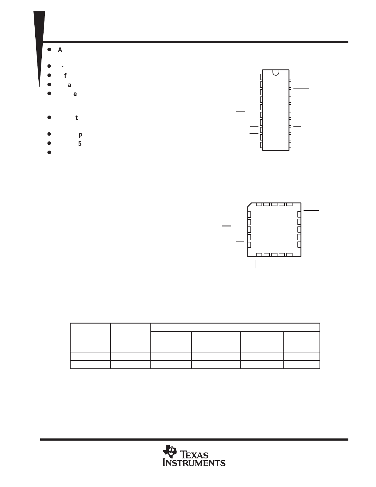
DB, DW, OR N PACKAGE
(TOP VIEW)
ANLG IN
(LSB) D0
D1
D2
D3
WR
/RDY
MODE
RD
INT
GND
1
2
3
4
5
6
7
8
9
10
FN PACKAGE
(TOP VIEW)
20
19
18
17
16
15
14
13
12
11
V
CC
NC
OFLW
D7 (MSB)
D6
D5
D4
CS
REF+
REF–
The TLC0820AC and the TLC0820AI are
Advanced LinCMOS 8-bit analog-to-digital
converters each consisting of two 4-bit flash
converters, a 4-bit digital-to-analog converter, a
summing (error) amplifier, control logic, and a
result latch circuit. The modified flash technique
allows low-power integrated circuitry to complete
an 8-bit conversion in 1.18 µs over temperature.
The on-chip track-and-hold circuit has a 100-ns
sample window and allows these devices to
convert continuous analog signals having slew
rates of up to 100 mV/µs without external
sampling components. TTL-compatible 3-state
D1
3 2 1 20 19
4
5
6
7
8
910111213
WR
D2
D3
/RDY
MODE
RD
INT
NC–No internal connection
CC
D0 (LSB)
ANLG IN
V
GND
REF+
REF –
NC
18
17
16
15
14
CS
OFLW
D7 (MSB)
D6
D5
D4
output drivers and two modes of operation allow
interfacing to a variety of microprocessors. Detailed information on interfacing to most popular microprocessors
is readily available from the factory.
AVAILABLE OPTIONS
PACKAGE
T
A
0°C to 70°C ±1 LSB TLC0820ACDB TLC0820ACDW TLC0820ACFN TLC0820ACN
–40°C to 85°C ±1 LSB — TLC0820AIDW TLC0820AIFN TLC0820AIN
UNADJUSTED
ERROR
SSOP
(DB)
PLASTIC
SMALL OUTLINE
(DW)
PLASTIC
CHIP CARRIER
(FN)
PLASTIC DIP
(N)
Advanced LinCMOS is a trademark of Texas Instruments Incorporated.
PRODUCTION DATA information is current as of publication date.
Products conform to specifications per the terms of Texas Instruments
standard warranty. Production processing does not necessarily include
testing of all parameters.
POST OFFICE BOX 655303 • DALLAS, TEXAS 75265
Copyright 1994, Texas Instruments Incorporated
2–1
TLC0820AC, TLC0820AI
Advanced LinCMOS HIGH-SPEED 8-BIT ANALOG-TO-DIGITAL
CONVERTERS USING MODIFIED FLASH TECHNIQUES
SLAS064A – SEPTEMBER 1986 – REVISED JUNE 1994
functional block diagram
12
REF+
REF–
ANLG IN
11
Summing
Amplifier
–1
1
+1
4-Bit Flash
Analog-to-Digital
Converter
(4 MSBs)
4-Bit
Digital-to-Analog
Converter
4-Bit Flash
Analog-to-Digital
Converter
(4 LSBs)
44
4
Output
Latch
and
3-State
Buffers
4
18
OFLW
2
D0 (LSB)
3
D1
4
D2
5
D3
14
D4
15
D5
16
D6
17
D7 (MSB)
Digital
Outputs
WR
MODE
/RDY
CS
RD
7
6
13
8
Timing
and
Control
9
INT
2–2
POST OFFICE BOX 655303 • DALLAS, TEXAS 75265
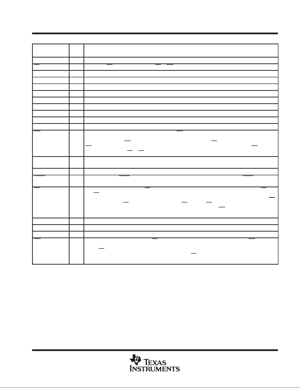
I/O
DESCRIPTION
TLC0820AC, TLC0820AI
Advanced LinCMOS HIGH-SPEED 8-BIT ANALOG-TO-DIGITAL
CONVERTERS USING MODIFIED FLASH TECHNIQUES
SLAS064A – SEPTEMBER 1986 – REVISED JUNE 1994
Terminal Functions
TERMINAL
NAME NO.
ANLG IN 1 I Analog input
CS 13 I Chip select. CS must be low in order for RD or WR to be recognized by the ADC.
D0 2 O Digital, 3-state output data, bit 1 (LSB)
D1 3 O Digital, 3-state output data, bit 2
D2 4 O Digital, 3-state output data, bit 3
D3 5 O Digital, 3-state output data, bit 4
D4 14 O Digital, 3-state output data, bit 5
D5 15 O Digital, 3-state output data, bit 6
D6 16 O Digital, 3-state output data, bit 7
D7 17 O Digital, 3-state output data, bit 8 (MSB)
GND 10 Ground
INT 9 O Interrupt. In the write-read mode, the interrupt output (INT) going low indicates that the internal count-down delay
MODE 7 I Mode select. MODE is internally tied to GND through a 50-µA current source, which acts like a pulldown resistor .
NC 19 No internal connection
OFLW 18 O Overflow . Normally OFL W is a logical high. However , if the analog input is higher than V
RD 8 I Read. In the write-read mode with CS low, the 3-state data outputs D0 through D7 are activated when RD goes
REF– 11 I Reference voltage. REF– is placed on the bottom of the resistor ladder.
REF+ 12 I Reference voltage. REF+ is placed on the top of the resistor ladder.
V
CC
WR/RDY 6 I/O Write ready . In the write-read mode with CS low, the conversion is started on the falling edge of the WR input signal.
20 Power supply voltage
time, t
after the rising edge of WR
INT
the rising edge of either RD
When MODE is low, the read mode is selected. When MODE is high, the write-read mode is selected.
the end of conversion. It can be used to cascade two or more devices to improve resolution (9 or 10 bits).
low. RD
count-down delay time. As a result, the data transferred to the output latch is latched after the falling edge of RD
In the read mode with CS
on completion of the conversion. RDY going into the high-impedance state and INT
of the conversion.
The result of the conversion is strobed into the output latch after the internal count-down delay time, t
that the RD
RDY (an open-drain output) goes low after the falling edge of CS
the conversion is strobed into the output latch. It is used to simplify the interface to a microprocessor system.
, is complete and the data result is in the output latch. The delay time t
d(int)
goes low at the end of t
can also be used to increase the conversion speed by reading data prior to the end of the internal
input does not go low prior to this time. The delay time t
(see operating characteristics and Figure 3). If RD goes low prior to the end of t
and the conversion results are available sooner (see Figure 2). INT is reset by
d(RIL)
or CS.
low, the conversion starts with RD going low . RD also enables the 3-state data outputs
is approximately 800 ns. In the read mode,
d(int)
and goes into the high-impedance state when
is typically 800 ns starting
d(int)
, OFLW will be low at
ref+
going low indicate completion
d(int)
d(int)
, provided
,
.
POST OFFICE BOX 655303 • DALLAS, TEXAS 75265
2–3
TLC0820AC, TLC0820AI
High-level input voltage, V
V
V
V
Low-level input voltage, V
V
V
V
Operating free-air temperature, T
°C
Advanced LinCMOS HIGH-SPEED 8-BIT ANALOG-TO-DIGITAL
CONVERTERS USING MODIFIED FLASH TECHNIQUES
SLAS064A – SEPTEMBER 1986 – REVISED JUNE 1994
absolute maximum ratings over operating free-air temperature range (unless otherwise noted)
(see Note 1) 10 V. . . . . . . . . . . . . . . . . . . . . . . . . . . . . . . . . . . . . . . . . . . . . . . . . . . . . . . . . . .
Supply voltage, V
Input voltage range, all inputs (see Note 1) –0.2 V to V
Output voltage range, all outputs (see Note 1) –0.2 V to V
CC
+0.2 V. . . . . . . . . . . . . . . . . . . . . . . . . . . . . . . . . . . . .
CC
+0.2 V. . . . . . . . . . . . . . . . . . . . . . . . . . . . . . . . . .
CC
Operating free-air temperature range: TLC0820AC 0°C to 70°C. . . . . . . . . . . . . . . . . . . . . . . . . . . . . . . . . . . . .
TLC0820AI –40°C to 85°C. . . . . . . . . . . . . . . . . . . . . . . . . . . . . . . . . . . .
Storage temperature range –65°C to 150°C. . . . . . . . . . . . . . . . . . . . . . . . . . . . . . . . . . . . . . . . . . . . . . . . . . . . . . . .
Case temperature for 10 seconds: FN package 260°C. . . . . . . . . . . . . . . . . . . . . . . . . . . . . . . . . . . . . . . . . . . . . .
Lead temperature 1,6 mm (1/16 inch) from case for 10 seconds: DB, DW or N package 260°C. . . . . . . . . . .
†
Stresses beyond those listed under “absolute maximum ratings” may cause permanent damage to the device. These are stress ratings only, and
functional operation of the device at these or any other conditions beyond those indicated under “recommended operating conditions” is not
implied. Exposure to absolute-maximum-rated conditions for extended periods may affect device reliability.
NOTE 1: All voltages are with respect to network GND.
recommended operating conditions
MIN NOM MAX UNIT
Supply voltage, V
Analog input voltage –0.1 VCC+0.1 V
Positive reference voltage, V
Negative reference voltage, V
Pulse duration, write in write-read mode, t
p
CC
ref+
ref–
p
p
IH
IL
(see Figures 2, 3, and 4) 0.5 50 µs
w(W)
p
A
= 4.75 V to 5.25
CC
= 4.75 V to 5.25
CC
TLC0820AC 0 70
TLC0820AI –40 85
CS, WR/RDY, RD 2
MODE 3.5
CS, WR/RDY, RD 0.8
MODE 1.5
4.5 5 8 V
V
ref–
GND V
V
CC
ref+
V
V
°
†
2–4
POST OFFICE BOX 655303 • DALLAS, TEXAS 75265

D0 D7, INT, or
CC
,
,
VOLLow-level output voltage
D0 D7, OFLW, INT,
CC
,
V
WR/RDY
MODE
V
5 V
I
(g )
D0–D7 or WR/RDY
A
V
0
CS at 5 V
V
V
IIAnalog input current
A
CS at 5 V
V
0
,
D0 D7, OFLW, INT,
V
V
IOSShort-circuit output current
D0–D7
OFLW
mA
V
0
INT
R
Reference resistance
kΩ
ICCSupply current
CS, WR/RDY, and
mA
CiInput capacitance
Full range
pF
TLC0820AC, TLC0820AI
Advanced LinCMOS HIGH-SPEED 8-BIT ANALOG-TO-DIGITAL
CONVERTERS USING MODIFIED FLASH TECHNIQUES
SLAS064A – SEPTEMBER 1986 – REVISED JUNE 1994
electrical characteristics at specified operating free-air temperature, VCC = 5 V (unless otherwise
noted)
PARAMETER TEST CONDITIONS T
D
–D7
V
I
I
C
†
High-level output voltage
OH
p
High-level input current
IH
Low-level input current
IL
Off-state (high-impedance-state)
OZ
output current
p
p
ref
pp
p
p
Output capacitance D0–D7 Full range 5 pF
o
Full range is as specified in recommended operating conditions.
INT r
OFLW
D0–D7, OFLW, INT
or WR/RDY
CS or RD Full range 0.005 1
CS, WR/RDY, RD,
or MODE
D0–D7, OFLW, INT
or WR/RDY
or
D0–D7
ANLG IN
VCC = 4.75 V,
IOH = –360 µA
V
= 4.75 V,
IOH = –10 µA
V
= 5.25 V,
IOL = 1.6 mA
VIH = 5 V
VIL = 0 Full range –0.005 –1 µA
=
O
=
O
,
= 5
I
,
=
I
= 5
O
=
O
CS, WR/RDY, and
RD at 0 V
†
A
Full range 2.4
Full range 4.5
25°C 4.6
Full range 0.4
25°C 0.34
Full range 3
25°C 0.1 0.3
Full range 200
25°C 50 170
Full range 3
25°C 0.1 0.3
Full range –3
25°C –0.1 –0.3
Full range 3
25°C 0.3
Full range –3
25°C –0.3
Full range 7
25°C 8.4 14
Full range –6
25°C –7.2 –12
Full range –4.5
25°C – 5.3 –9
Full range 1.25 6
25°C 1.4 2.3 5.3
Full range 15
25°C 7.5 13
MIN TYP MAX UNIT
5
45
V
µA
µ
µ
p
POST OFFICE BOX 655303 • DALLAS, TEXAS 75265
2–5

TLC0820AC, TLC0820AI
t
A
RD↓ to dat
lid
t
t
ns
t
A
RD↓ to dat
lid
t
t
ns
t
di
Disable time, RD↑ to data valid
70
95
ns
t
d(int)
Delay time, WR/RDY↑ to INT↓
800
1300
ns
t
d(RDY)
Delay time, CS↓ to WR/RDY↓
50
100
ns
t
d(RIL)
Delay time, RD↓ to INT↓
200
290
ns
t
d(WIH)
Delay time, WR/RDY↑ to INT↑
175
270
ns
Advanced LinCMOS HIGH-SPEED 8-BIT ANALOG-TO-DIGITAL
CONVERTERS USING MODIFIED FLASH TECHNIQUES
SLAS064A – SEPTEMBER 1986 – REVISED JUNE 1994
operating characteristics, VCC = 5 V , V
ref+
= 5 V , V
= 0, tr = tf = 20 ns, TA = 25°C (unless otherwise
ref–
noted)
< t
†
d(int)
MIN TYP MAX UNIT
t
conv(R)
,
PARAMETER TEST CONDITIONS
k
SVS
t
conv(R)
t
a(R)
a(R1)
a(R2)
t
a(INT)
s
t
d(NC)
t
d(WR)
t
d(RIH)
†
For conditions shown as MIN or MAX, use the appropriate value specified under recommended operating conditions.
‡
Total unadjusted error includes offset, full-scale, and linearity errors.
Supply-voltage sensitivity VCC = 5 V ± 5%, TA = MIN to MAX ±1/16 ±1/4 LSB
Total unadjusted error
Conversion time, read mode MODE at 0 V, See Figure 1 1.6 2.5 µs
Access time, RD↓ to data valid
ccess time,
ccess time,
Access time, INT↓ to data valid MODE at 5 V, See Figure 4 20 50 ns
Delay time, to next conversion See Figures 1, 2, 3, and 4 500 ns
Delay time, WR/RDY↑ to RD↓ in
write-read mode
Delay time, RD↑ to INT↑
Slew-rate tracking 0.1 V/µs
‡
a va
a va
MODE at 0 V, TA = MIN to MAX 1 LSB
MODE at 0 V, See Figure 1
MODE at 5 V,
<
d(WR)
See Figure 2
MODE at 5 V,
d(WR)
See Figure 3
RL = 1 kΩ, CL = 10 pF,
See Figures 1, 2, 3, and 5
MODE at 5 V, CL = 50 pF,
See Figures 2, 3, and 4
See Figure 2 0.4 µs
MODE at 0 V, CL = 50 pF,
See Figure 1
CL = 50 pF, See Figures 1, 2, and 3 125 225 ns
MODE at 5 V, t
See Figure 2
MODE at 5 V, CL = 50 pF,
See Figure 4
>
d(int)
d(int)
CL = 15 pF 190 280
,
CL = 100 pF 210 320
CL = 15 pF 70 120
,
CL = 100 pF 90 150
d(WR)
+20
t
conv(R)
+50
ns
2–6
POST OFFICE BOX 655303 • DALLAS, TEXAS 75265

)
)
s
H
)
)
TLC0820AC, TLC0820AI
Advanced LinCMOS HIGH-SPEED 8-BIT ANALOG-TO-DIGITAL
CONVERTERS USING MODIFIED FLASH TECHNIQUES
SLAS064A – SEPTEMBER 1986 – REVISED JUNE 1994
PARAMETER MEASUREMENT INFORMATION
CS
RD
WR/RDY
INT
D0–D7
50%
Figure 1. Read-Mode Waveforms (MODE Low)
CS
t
w(W)
WR/RDY
RD
INT
D0–D7
t
d(WR)
t
d(int)
50%50% 50%
t
d(RIL)
t
a(R1)
50% 50%
50% 50%
90%
10%
Figure 2. Write-Read-Mode Waveforms
[MODE High and t
d(WR
< t
50% 50%
50%
t
d(RDY)
t
conv(R)
90%
10%
t
a(R)
WR/RDY
t
d(NC)
t
d(RIH)
90%
10%
t
dis
]
d(int
With External Pullup
50% 50%
CS
t
w(W)
50%
RD
INT
D0–D7
Figure 3. Write-Read-Mode Waveforms
50%
t
d(NC)
t
d(RIH)
90%
10%
t
dis
50%
t
d(WR)
50% 50%
t
d(int)
t
a(R2)
[MODE High and t
t
d(NC)
50% 50%
90%
10%
> t
d(WR
d(int
t
d(RI
90%
10%
t
di
]
POST OFFICE BOX 655303 • DALLAS, TEXAS 75265
2–7

TLC0820AC, TLC0820AI
Advanced LinCMOS HIGH-SPEED 8-BIT ANALOG-TO-DIGITAL
CONVERTERS USING MODIFIED FLASH TECHNIQUES
SLAS064A – SEPTEMBER 1986 – REVISED JUNE 1994
PARAMETER MEASUREMENT INFORMATION
CS
Low
RD
Low
t
w(W)
/RDY
WR
INT
D0– D7
Figure 4. Write-Read-Mode Waveforms
(Stand-Alone Operation, MODE High, and RD
50%50% 50%
t
d(WIH)
50% 50%
t
d(int)
90%
10%
t
d(NC)
t
a(INT)
Data Valid
Low)
TLC0820
Input
TLC0820
Input
RD
CS
RD
CS
V
GND
V
GND
CC
CC
Dn
Dn
CL1 kΩ
1 kΩ
C
Data
Output
Data
Output
L
RD
Data
Outputs
tr = 20 ns
RD
Data
Outputs
tr = 20 ns
t
r
t
dis
VOLTAGE WAVEFORMSTEST CIRCUIT
t
r
t
dis
CL = 10 pF
50%
10%
CL = 10 pF
50%
10%
90%
90%
90%
10%
V
CC
GND
V
OH
GND
V
CC
GND
V
CC
V
OL
2–8
Dn = D0...D7
VOLTAGE WAVEFORMS
TEST CIRCUIT
Figure 5. Test Circuit and Voltage Waveforms
POST OFFICE BOX 655303 • DALLAS, TEXAS 75265

TLC0820AC, TLC0820AI
Advanced LinCMOS HIGH-SPEED 8-BIT ANALOG-TO-DIGITAL
CONVERTERS USING MODIFIED FLASH TECHNIQUES
SLAS064A – SEPTEMBER 1986 – REVISED JUNE 1994
PRINCIPLES OF OPERATION
The TLC0820AC and TLC0820AI each employ a combination of sampled-data comparator techniques and flash
techniques common to many high-speed converters. Two 4-bit flash analog-to-digital conversions are used to give
a full 8-bit output.
The recommended analog input voltage range for conversion is –0.1 V to V
less than V
inputs are fully differential with common-mode limits defined by the supply rails. The reference input values define
the full-scale range of the analog input. This allows the gain of the ADC to be varied for ratiometric conversion by
changing the V
The device operates in two modes, read (only) and write-read, that are selected by MODE. The converter is set to
the read (only) mode when MODE is low. In the read mode, WR
ready terminal. In this mode, a low on WR
on the falling edge of RD
high-impedance state. Data outputs also change from high-impedance to active states at this time. After the data is
read, RD
When MODE is high, the converter is set to the write-read mode and WR
Taking CS
600 ns after WR
in the write-read mode.
The high-order 4-bit flash ADC measures the input by means of 16 comparators operating simultaneously. A
high-precision 4-bit DAC then generates a discrete analog voltage from the result of that conversion. After a time
delay , a second bank of comparators does a low-order conversion on the analog difference between the input level
and the high-order DAC output. The results from each of these conversions enter an 8-bit latch and are output to the
3-state output buffers on the falling edge of RD
+ 1/2 LSB or greater than V
ref–
and V
ref+
is taken high, INT returns high, and the data outputs return to their high-impedance states.
and WR/RDY low selects the converter and initiates measurement of the input signal. Approximately
/RDY returns high, the conversion is completed. Conversion starts on the rising edge of WR/RDY
voltages.
ref–
and is completed no more than 2.5 µs later when INT falls and WR/RDY returns to the
– 1/2 LSB convert to 00000000 or 11111111, respectively. The reference
ref+
/RDY is used as an output and is referred to as the
/RDY while CS is low indicates that the device is busy . Conversion starts
.
+ 0.1 V . Analog input signals that are
CC
/RDY is referred to as the write terminal.
POST OFFICE BOX 655303 • DALLAS, TEXAS 75265
2–9

TLC0820AC, TLC0820AI
Advanced LinCMOS HIGH-SPEED 8-BIT ANALOG-TO-DIGITAL
CONVERTERS USING MODIFIED FLASH TECHNIQUES
SLAS064A – SEPTEMBER 1986 – REVISED JUNE 1994
APPLICATION INFORMATION
µP
Bus
CS
WR
RD
D0
D1
D2
D3
D4
D5
D6
D7
D8
OFL
13
6
8
2
3
4
5
14
15
16
17
18
13
6
CS
WR/RDY
RD
TLC0820
D0
D1
D2
D3
D4
D5
D6
D7
OFLW
CS
WR/RDY
V
CC
ANLG
IN
MODE
REF+
REF–
GND
V
CC
ANLG
IN
20
20
12
11
10
5 V
1
7
5 V
5 V
1
5 V
0.1
0.1
ANLG
IN
µF
µF
8
RD
TLC0820
2
14
15
16
17
18
3
4
5
D0
D1
D2
D3
D4
D5
D6
D7
OFLW
MODE
REF+
REF–
GND
Figure 6. Configuration for 9-Bit Resolution
12
10
7
5 V
0.1 µF
11
0.1 µF
2–10
POST OFFICE BOX 655303 • DALLAS, TEXAS 75265

IMPORTANT NOTICE
T exas Instruments and its subsidiaries (TI) reserve the right to make changes to their products or to discontinue
any product or service without notice, and advise customers to obtain the latest version of relevant information
to verify, before placing orders, that information being relied on is current and complete. All products are sold
subject to the terms and conditions of sale supplied at the time of order acknowledgement, including those
pertaining to warranty, patent infringement, and limitation of liability.
TI warrants performance of its semiconductor products to the specifications applicable at the time of sale in
accordance with TI’s standard warranty. Testing and other quality control techniques are utilized to the extent
TI deems necessary to support this warranty . Specific testing of all parameters of each device is not necessarily
performed, except those mandated by government requirements.
CERT AIN APPLICATIONS USING SEMICONDUCTOR PRODUCTS MAY INVOL VE POTENTIAL RISKS OF
DEATH, PERSONAL INJURY, OR SEVERE PROPERTY OR ENVIRONMENTAL DAMAGE (“CRITICAL
APPLICATIONS”). TI SEMICONDUCTOR PRODUCTS ARE NOT DESIGNED, AUTHORIZED, OR
WARRANTED TO BE SUITABLE FOR USE IN LIFE-SUPPORT DEVICES OR SYSTEMS OR OTHER
CRITICAL APPLICA TIONS. INCLUSION OF TI PRODUCTS IN SUCH APPLICATIONS IS UNDERST OOD TO
BE FULLY AT THE CUSTOMER’S RISK.
In order to minimize risks associated with the customer’s applications, adequate design and operating
safeguards must be provided by the customer to minimize inherent or procedural hazards.
TI assumes no liability for applications assistance or customer product design. TI does not warrant or represent
that any license, either express or implied, is granted under any patent right, copyright, mask work right, or other
intellectual property right of TI covering or relating to any combination, machine, or process in which such
semiconductor products or services might be or are used. TI’s publication of information regarding any third
party’s products or services does not constitute TI’s approval, warranty or endorsement thereof.
Copyright 1998, Texas Instruments Incorporated
 Loading...