

TL343
SINGLE LOW-POWER OPERATIONAL AMPLIFIER
SLOS250D – JUNE 1999 – REVISED NOVEMBER 1999
D
Wide Range of Supply Voltages, Single
Supply 5 V to 30 V, or Dual Supplies
D
Class AB Output Stage
D
True Differential-Input Stage
D
Low Input Bias Current
D
Internal Frequency Compensation
D
Short-Circuit Protection
D
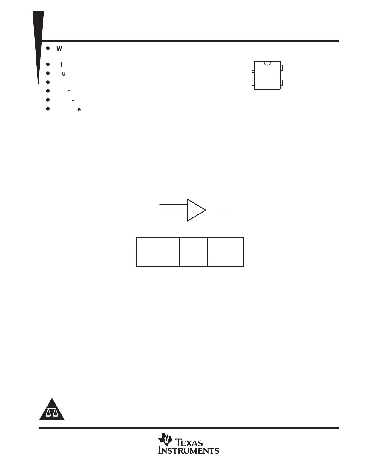
Packaged in SOT-23 Package
V
CC–
DBV PACKAGE
IN+
/GND
IN–
(TOP VIEW)
1
2
3
5
4
V
CC
OUT
+
description
The TL343 is a single operational amplifier similar in performance to the µA741, but with several distinct
advantages. It is designed to operate from a single supply over a range of voltages from 3 V to 36 V . Operation
from split supplies also is possible, provided the difference between the two supplies is 3 V to 36 V. The
common-mode input range includes the negative supply. Output range is from the negative supply to
V
– 1.5 V.
CC
The TL343 is characterized for operation from –40°C to 125°C.
symbol
IN+
IN–
+
–
OUT
AVAILABLE OPTIONS
T
A
–40°C to 125°C 10 mV TL343IDBV
The DBV package is only available taped and
reeled. Add the suffix R to device type for ordering
(e.g., TL343IDBVR).
VIOMAX
AT 25°C
SOT-23
PACKAGE
(DBV)
Please be aware that an important notice concerning availability, standard warranty, and use in critical applications of
Texas Instruments semiconductor products and disclaimers thereto appears at the end of this data sheet.
PRODUCTION DATA information is current as of publication date.
Products conform to specifications per the terms of Texas Instruments
standard warranty. Production processing does not necessarily include
testing of all parameters.
POST OFFICE BOX 655303 • DALLAS, TEXAS 75265
Copyright 1999, Texas Instruments Incorporated
1
TL343
Suppl
oltage (see Note 1)
V
SINGLE LOW-POWER OPERATIONAL AMPLIFIER
SLOS250D – JUNE 1999 – REVISED NOVEMBER 1999
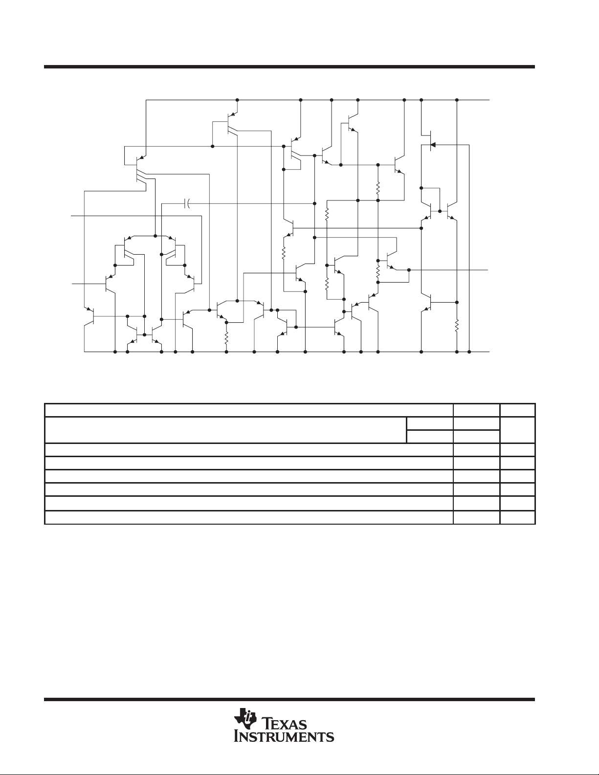
schematic
5 pF
IN+
IN–
V
OUT
CC+
2.4 kΩ
V
/GND
CC–
NOTE A: Component values shown are nominal.
absolute maximum ratings over operating free-air temperature range (unless otherwise noted)
MAX UNIT
V
pp
y v
Supply voltage, V
Differential input voltage (see Note 2) ±36 V
Input voltage (see Notes 1 and 3) ±18 V
Package thermal impedance, θJA (see Note 4) 347 °C/W
Lead temperature 1,6 mm (1/16 inch) from case for 10 seconds 260 °C
Storage temperature range, T
NOTES: 1. These voltage values are with respect to the midpoint between V
2. Differential voltages are at IN+ with respect to IN–.
3. Neither input must ever be more positive than V
4. The package thermal impedance is calculated in accordance with JESD 51.
with respect to V
CC+
stg
CC–
CC+
or more negative than V
CC+
and V
CC–
CC–
.
.
V
CC+
CC–
18
–18
36 V
–65 to 150 °C
2
POST OFFICE BOX 655303 • DALLAS, TEXAS 75265
Dual-suppl
oltage
V
VIOInput offset voltage
See Note 5
mV
IIOInput offset current
See Note 5
nA
IIBInput bias current
See Note 5
nA
R
kΩ
A
gg
V
±10 V
R
kΩ
V/mV
SINGLE LOW-POWER OPERATIONAL AMPLIFIER
SLOS250D – JUNE 1999 – REVISED NOVEMBER 1999
recommended operating conditions
Single-supply voltage V
pp
y v
Operating free-air temperature, T
A
V
V
CC
CC+
CC–
TL343
MIN MAX UNIT
5 30 V
2.5 15
–2.5 –15
–40 125 °C
electrical characteristics at specified free-air temperature, V
PARAMETER
p
a
a
I
V
ICR
V
OM
VD
B
OM
B
1
φ
m
r
i
r
o
CMRR Common-mode rejection ratio VIC = V
k
SVS
I
OS
I
CC
†
All characteristics are measured under open-loop conditions with zero common-mode voltage unless otherwise specified. Full range for TA is
–40°C to 125°C.
‡
The V
§
Temperature and/or supply voltages must be limited to ensure that the dissipation rating is not exceeded.
NOTE 5: VIO, IIO, IIB, and ICC are defined at VO = 0.
Temperature coefficient
V
IO
of input offset voltage
p
Temperature coefficient
IO
of input offset current
p
Common-mode input voltage range
Peak output-voltage swing
Large-signal differential
voltage amplification
Maximum-output-swing bandwidth
Unity-gain bandwidth VO = 50 mV, RL = 10 kΩ 25°C 1 MHz
Phase margin CL = 200 pF, RL = 2 kΩ 25°C 44°
Input resistance f = 20 Hz 25°C 0.3 1 MΩ
Output resistance f = 20 Hz 25°C 75 Ω
Supply-voltage sensitivity (∆VIO/∆VCC) V
Short-circuit output current
Total supply current No load, See Note 5 25°C 0.7 2.8 mA
limits are linked directly, volt-for-volt, to supply voltage; the positive limit is 2 V less than V
ICR
§
‡
See Note 5 Full range 10 µV/°C
See Note 5 Full range 50 pA/C
RL = 10 kΩ 25°C ±12 ±13.5
= 2
L
=
O
V
OPP
THD ≤ 5%,
CC±
TEST CONDITIONS
,
= 20 V,
(min) 25°C 70 90 dB
ICR
= ±2.5 to ±15 V 25°C 30 150 µV/V
= 2
L
AVD = 1,
RL = 2 kΩ
= ±15 V (unless otherwise noted)
±
CC
†
25°C 2 10
Full range 12
25°C 30 50
Full range 200
25°C –20 –50
Full range –80
25°C
25°C ±10 ±13
Full range ±10
25°C 20 200
Full range 15
25°C 9 kHz
25°C ±10 ±30 ±55 mA
MIN TYP MAX UNIT
CC+
V
.
CC–
to 13
V
CC–
to 13.5
V
V
POST OFFICE BOX 655303 • DALLAS, TEXAS 75265
3

TL343
SINGLE LOW-POWER OPERATIONAL AMPLIFIER
SLOS250D – JUNE 1999 – REVISED NOVEMBER 1999
electrical characteristics, V
PARAMETER
V
I
IO
I
IB
V
A
k
I
CC
†
All characteristics are measured under open-loop conditions with zero common-mode input voltage unless otherwise specified.
‡
Output swings essentially to ground.
Input offset voltage VO = 2.5 V 2 10 mV
IO
Input offset current VO = 2.5 V 30 50 nA
Input bias current VO = 2.5 V –20 –50 nA
Peak output voltage swing
OM
Large-signal differential voltage
VD
amplification
Supply-voltage sensitivity (∆VIO/∆V
SVS
Supply current VO = 2.5 V, No load 0.7 1.75 mA
operating characteristics, V
PARAMETER TEST CONDITIONS MIN TYP MAX UNIT
SR Slew rate at unity gain VI = ±10 V, CL = 100 pF, RL = 2 kΩ, See Figure 1 1 V/µs
t
Rise time ∆VO = 50 mV, CL = 100 pF, RL = 10 kΩ, See Figure 1 0.35 µs
r
t
Fall time ∆VO = 50 mV, CL = 100 pF, RL = 10 kΩ, See Figure 1 0.35 µs
f
Overshoot factor ∆VO = 50 mV, CL = 100 pF, RL = 10 kΩ, See Figure 1 20%
Crossover distortion V
CC+
‡
CC
= 30 mV, V
I(PP)
= 5 V, V
) V
CC±
=
±15 V, T
±
= 0 V, TA = 25°C (unless otherwise noted)
CC–
TEST CONDITIONS
RL = 10 kΩ 3.3 3.5 V
VO = 1.7 V to 3.3 V, RL = 2 kΩ 20 200 V/mV
= ±2.5 V to ±15 V 150 µV/V
CC±
= 25°C, AVD = 1 (unless otherwise noted)
A
= 2 V, f = 10 kHZ 1%
OPP
†
MIN TYP MAX UNIT
PARAMETER MEASUREMENT INFORMATION
–
I
CL = 100 pF
+
V
Figure 1. Unity-Gain Amplifier
OUT
R
L
4
POST OFFICE BOX 655303 • DALLAS, TEXAS 75265

TL343
SINGLE LOW-POWER OPERATIONAL AMPLIFIER
SLOS250D – JUNE 1999 – REVISED NOVEMBER 1999
INPUT BIAS CURRENT
FREE-AIR TEMPERATURE
250
V
= ±15 V
CC±
200
150
100
– Input Bias Current – nA
IB
I
50
0
–50 –25 0 25 50 75 100 125
–75
TA – Free-Air Temperature – °C
vs
Figure 2
TYPICAL CHARACTERISTICS
250
TA = 25°C
200
150
100
– Input Bias Current – nA
IB
I
50
0
0
†
INPUT BIAS CURRENT
SUPPLY VOLTAGE
2 4 8 101214166
|V
| – Supply Voltage – V
CC±
Figure 3
vs
MAXIMUM PEAK-TO-PEAK OUTPUT VOLTAGE
vs
SUPPLY VOLTAGE
30
RL = 10 kΩ
TA = 25°C
25
20
15
10
5
– Maximum Peak-to-Peak Output Voltage – V
OPP
V
0
0
2 4 6 8 10 12 14 16
|V
| – Supply Voltage – V
CC±
Figure 4
MAXIMUM PEAK-TO-PEAK OUTPUT VOLTAGE
vs
FREQUENCY
30
25
20
15
10
5
– Maximum Peak-to-Peak Output Voltage – V
OPP
V
0
1 k
10 k
f – Frequency – Hz
V
CC±
CL = 0
RL = 10 kΩ
TA = 25°C
See Figure 1
100 k
= ±15 V
Figure 5
1 M
†
Operation of the device at these or any other conditions beyond those indicated under “recommended operating conditions” is not implied.
POST OFFICE BOX 655303 • DALLAS, TEXAS 75265
5

TL343
SINGLE LOW-POWER OPERATIONAL AMPLIFIER
SLOS250D – JUNE 1999 – REVISED NOVEMBER 1999
TYPICAL CHARACTERISTICS
LARGE-SIGNAL
DIFFERENTIAL VOLTAGE AMPLIFICATION
vs
6
10
5
10
4
10
3
10
2
10
10
– Large-Signal Differential Voltage Amplification – dB
1
1
A
VD
10 100 1 k 10 k 100 k 1 M
FREQUENCY
f – Frequency – Hz
Figure 6
V
CC±
RL = 2 kΩ
TA = 25°C
= ±15 V
10
5
0
–5
Input/Output Voltages – V
–10
†
VOLTAGE-FOLLOWER
LARGE-SIGNAL PULSE RESPONSE
V
= ±15 V
CC±
RL = 2 kΩ
TA = 25°C
Output
0 102030405060708090
t – Time –µs
See Figure 1
Input
Figure 7
†
Operation of the device at these or any other conditions beyond those indicated under “recommended operating conditions” is not implied.
6
POST OFFICE BOX 655303 • DALLAS, TEXAS 75265

IMPORTANT NOTICE
T exas Instruments and its subsidiaries (TI) reserve the right to make changes to their products or to discontinue
any product or service without notice, and advise customers to obtain the latest version of relevant information
to verify, before placing orders, that information being relied on is current and complete. All products are sold
subject to the terms and conditions of sale supplied at the time of order acknowledgement, including those
pertaining to warranty, patent infringement, and limitation of liability.
TI warrants performance of its semiconductor products to the specifications applicable at the time of sale in
accordance with TI’s standard warranty. Testing and other quality control techniques are utilized to the extent
TI deems necessary to support this warranty . Specific testing of all parameters of each device is not necessarily
performed, except those mandated by government requirements.
CERTAIN APPLICATIONS USING SEMICONDUCTOR PRODUCTS MAY INVOLVE POTENTIAL RISKS OF
DEATH, PERSONAL INJURY, OR SEVERE PROPERTY OR ENVIRONMENTAL DAMAGE (“CRITICAL
APPLICATIONS”). TI SEMICONDUCTOR PRODUCTS ARE NOT DESIGNED, AUTHORIZED, OR
WARRANTED TO BE SUITABLE FOR USE IN LIFE-SUPPORT DEVICES OR SYSTEMS OR OTHER
CRITICAL APPLICA TIONS. INCLUSION OF TI PRODUCTS IN SUCH APPLICATIONS IS UNDERST OOD TO
BE FULLY AT THE CUSTOMER’S RISK.
In order to minimize risks associated with the customer’s applications, adequate design and operating
safeguards must be provided by the customer to minimize inherent or procedural hazards.
TI assumes no liability for applications assistance or customer product design. TI does not warrant or represent
that any license, either express or implied, is granted under any patent right, copyright, mask work right, or other
intellectual property right of TI covering or relating to any combination, machine, or process in which such
semiconductor products or services might be or are used. TI’s publication of information regarding any third
party’s products or services does not constitute TI’s approval, warranty or endorsement thereof.
Copyright 1999, Texas Instruments Incorporated
 Loading...