

Page 1
TL331
SINGLE DIFFERENTIAL COMPARATOR
SLVS238A – AUGUST 1999 – REVISED NOVEMBER 1999
1
POST OFFICE BOX 655303 • DALLAS, TEXAS 75265
D
Single Supply or Dual Supplies
D
Wide Range of Supply Voltage
...2 V to 36 V
D
Low Supply-Current Drain Independent of
Supply Voltage . . . 0.4 mA Typ
D
Low Input Bias Current . . . 25 nA Typ
D
Low Input Offset Voltage ...2 mV Typ
D
Common-Mode Input Voltage Range
Includes Ground
D
Differential Input Voltage Range Equal to
Maximum-Rated Supply V oltage . . . ±36 V
D
Low Output Saturation Voltage
D
Output Compatible With TTL, MOS, and
CMOS
D
Packaged in Plastic Small-Outline
Transistor Package
description
This device consists of a single voltage comparator that is designed to operate from a single power supply over
a wide range of voltages. Operation from dual supplies also is possible if the difference between the two supplies
is 2 V to 36 V and VCC is at least 1.5 V more positive than the input common-mode voltage. Current drain is
independent of the supply voltage. The output can be connected to other open-collector outputs to achieve
wired-AND relationships.
The TL331I is characterized for operation from –40°C to 85°C.
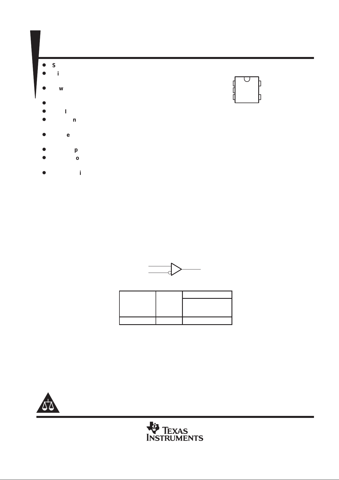
logic diagram
IN+
IN–
OUT
AVAILABLE OPTIONS
PACKAGED DEVICE
T
A
V
IO(max
)
AT 25°C
SMALL-OUTLINE
TRANSISTOR
(DBV)
–40°C to 85°C 5 mV TL331IDBV
The DBV package is only available left-end taped and
reeled. Add suffix R to device type (e.g., TL331IDBVR).
Copyright 1999, Texas Instruments Incorporated
PRODUCTION DATA information is current as of publication date.
Products conform to specifications per the terms of Texas Instruments
standard warranty. Production processing does not necessarily include
testing of all parameters.
Please be aware that an important notice concerning availability, standard warranty, and use in critical applications of
Texas Instruments semiconductor products and disclaimers thereto appears at the end of this data sheet.
DBV PACKAGE
(TOP VIEW)
1
2
3
5
4
IN–
V
CC–
/GND
IN+
V
CC
OUT
Page 2
TL331
SINGLE DIFFERENTIAL COMPARATOR
SLVS238A – AUGUST 1999 – REVISED NOVEMBER 1999
2
POST OFFICE BOX 655303 • DALLAS, TEXAS 75265
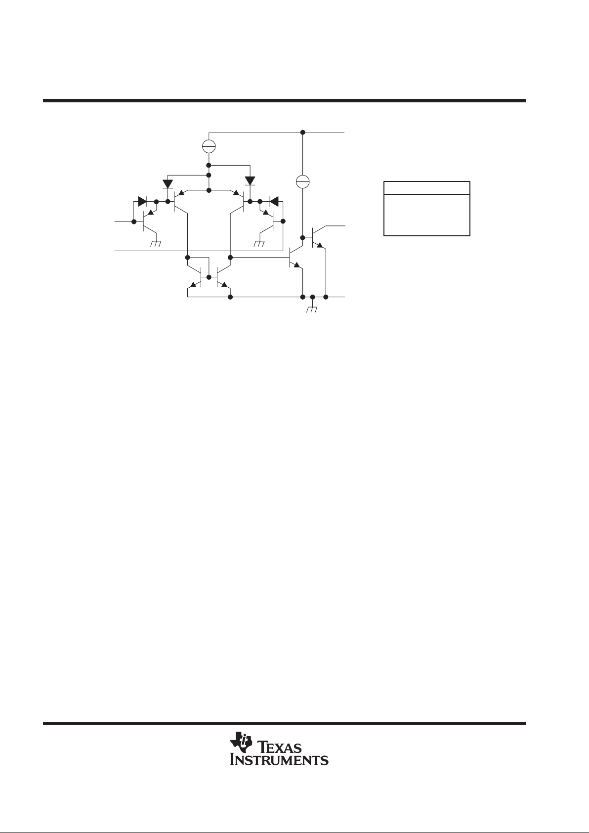
schematic
80-µA
Current Regulator
80 µA
60 µA
10 µA
V
CC
10 µA
OUT
GND
IN+
IN–
Epi-FET
Diodes
Resistors
Transistors
Current values shown are nominal.
COMPONENT COUNT
1
2
1
20
absolute maximum ratings over operating free-air temperature range (unless otherwise noted)
†
Supply voltage, VCC (see Note 1) 36 V. . . . . . . . . . . . . . . . . . . . . . . . . . . . . . . . . . . . . . . . . . . . . . . . . . . . . . . . . . . .
Differential input voltage, VID (see Note 2) ±36 V. . . . . . . . . . . . . . . . . . . . . . . . . . . . . . . . . . . . . . . . . . . . . . . . . . .
Input voltage range, VI (either input) –0.3 V to 36 V. . . . . . . . . . . . . . . . . . . . . . . . . . . . . . . . . . . . . . . . . . . . . . . . .
Output voltage, VO 36 V. . . . . . . . . . . . . . . . . . . . . . . . . . . . . . . . . . . . . . . . . . . . . . . . . . . . . . . . . . . . . . . . . . . . . . . . .
Output current, IO 20 mA. . . . . . . . . . . . . . . . . . . . . . . . . . . . . . . . . . . . . . . . . . . . . . . . . . . . . . . . . . . . . . . . . . . . . . . .
Duration of output short-circuit to ground (see Note 3) Unlimited. . . . . . . . . . . . . . . . . . . . . . . . . . . . . . . . . . . . . .
Package thermal impedance, θ
JA
(see Notes 4 and 5) 347°C/W. . . . . . . . . . . . . . . . . . . . . . . . . . . . . . . . . . . . . .
Operating free-air temperature range, TA –40°C to 85°C. . . . . . . . . . . . . . . . . . . . . . . . . . . . . . . . . . . . . . . . . . . .
Lead temperature 1,6 mm (1/16 inch) from case for 10 seconds 260°C. . . . . . . . . . . . . . . . . . . . . . . . . . . . . . .
Storage temperature range, T
stg
–65°C to 150°C. . . . . . . . . . . . . . . . . . . . . . . . . . . . . . . . . . . . . . . . . . . . . . . . . . .
†
Stresses beyond those listed under “absolute maximum ratings” may cause permanent damage to the device. These are stress ratings only, and
functional operation of the device at these or any other conditions beyond those indicated under “recommended operating conditions” is not
implied. Exposure to absolute-maximum-rated conditions for extended periods may affect device reliability.
NOTES: 1. All voltage values, except differential voltages, are with respect to the network ground.
2. Differential voltages are at IN+ with respect to IN–.
3. Short circuits from outputs to VCC can cause excessive heating and eventual destruction.
4. Maximum power dissipation is a function of TJ(max),
θ
JA
, and TA. The maximum allowable power dissipation at any allowable
ambient temperature is PD = (TJ(max) – TA)/
θ
JA
. Operating at the absolute maximum TJ of 150°C can impact reliability.
5. The package thermal impedance is calculated in accordance with JESD 51.
Page 3

TL331
SINGLE DIFFERENTIAL COMPARATOR
SLVS238A – AUGUST 1999 – REVISED NOVEMBER 1999
3
POST OFFICE BOX 655303 • DALLAS, TEXAS 75265
electrical characteristics at specified free-air temperature, VCC = 5 V (unless otherwise noted)
PARAMETER TEST CONDITIONS
T
A
†
MIN TYP MAX UNIT
p
V
= 5 V to 30 V, V
= 1.4 V,
25°C 2 5
VIOInput offset voltage
CC
,
O
,
VIC = V
IC(min)
–40°C to 85°C 9
mV
p
25°C 5 50
IIOInput offset current
V
O
= 1.4
V
–40°C to 85°C 250
nA
p
25°C –25 –250
IIBInput bias current
V
O
=
1.4 V
–40°C to 85°C –400
nA
Common-mode
25°C
0 to
VCC–1.5
V
ICR
input voltage range
‡
–40°C to 85°C
0 to
VCC–2
V
A
VD
Large-signal
differential voltage amplification
VCC = 15 V, VO = 1.4 V to 11.4 V,
RL ≥ 15 kΩ to V
CC
25°C 50 200 V/mV
p
VOH = 5 V, VID = 1 V 25°C 0.1 50 nA
IOHHigh-level output current
VOH = 30 V, VID = 1 V –40°C to 85°C 1 µA
p
25°C 150 400
VOLLow-level output voltage
I
OL
= 4 mA,
V
ID
= –1
V
–40°C to 85°C 700
mV
I
OL
Low-level output current VOL = 1.5 V, VID = 1 V 25°C 6 mA
I
CC
Supply current RL = ∞, VCC = 5 V 25°C 0.4 0.7 mA
†
All characteristics are measured with zero common-mode input voltage, unless otherwise specified.
‡
The voltage at either input or common-mode should not be allowed to go negative by more than 0.3 V . The upper end of the common-mode voltage
range is V
CC+
– 1.5 V , but either or both inputs can go to 30 V without damage.
switching characteristics, VCC = 5 V, TA = 25°C
PARAMETER TEST CONDITIONS MIN TYP MAX UNIT
p
RL connected to 5 V through 5.1 kΩ,
100-mV input step with 5-mV overdrive 1.3
Response time
L
g
CL = 15 pF§, See Note 6
TTL-level input step 0.3
µ
s
§
CL includes probe and jig capacitance.
NOTE 6: The response time specified is the interval between the input step function and the instant when the output crosses 1.4 V.
Page 4

IMPORTANT NOTICE
T exas Instruments and its subsidiaries (TI) reserve the right to make changes to their products or to discontinue
any product or service without notice, and advise customers to obtain the latest version of relevant information
to verify, before placing orders, that information being relied on is current and complete. All products are sold
subject to the terms and conditions of sale supplied at the time of order acknowledgement, including those
pertaining to warranty, patent infringement, and limitation of liability.
TI warrants performance of its semiconductor products to the specifications applicable at the time of sale in
accordance with TI’s standard warranty. Testing and other quality control techniques are utilized to the extent
TI deems necessary to support this warranty. Specific testing of all parameters of each device is not necessarily
performed, except those mandated by government requirements.
CERT AIN APPLICATIONS USING SEMICONDUCTOR PRODUCTS MAY INVOLVE POTENTIAL RISKS OF
DEATH, PERSONAL INJURY, OR SEVERE PROPERTY OR ENVIRONMENTAL DAMAGE (“CRITICAL
APPLICATIONS”). TI SEMICONDUCTOR PRODUCTS ARE NOT DESIGNED, AUTHORIZED, OR
WARRANTED TO BE SUITABLE FOR USE IN LIFE-SUPPORT DEVICES OR SYSTEMS OR OTHER
CRITICAL APPLICATIONS. INCLUSION OF TI PRODUCTS IN SUCH APPLICA TIONS IS UNDERSTOOD T O
BE FULLY AT THE CUSTOMER’S RISK.
In order to minimize risks associated with the customer’s applications, adequate design and operating
safeguards must be provided by the customer to minimize inherent or procedural hazards.
TI assumes no liability for applications assistance or customer product design. TI does not warrant or represent
that any license, either express or implied, is granted under any patent right, copyright, mask work right, or other
intellectual property right of TI covering or relating to any combination, machine, or process in which such
semiconductor products or services might be or are used. TI’s publication of information regarding any third
party’s products or services does not constitute TI’s approval, warranty or endorsement thereof.
Copyright 1999, Texas Instruments Incorporated
 Loading...