

CHIP
TL317
3-TERMINAL ADJUSTABLE REGULATORS
SLVS004C – APRIL 1979 – REVISED JULY 1999
D
Output V oltage Range Adjustable From
1.2 V to 32 V When Used With an External
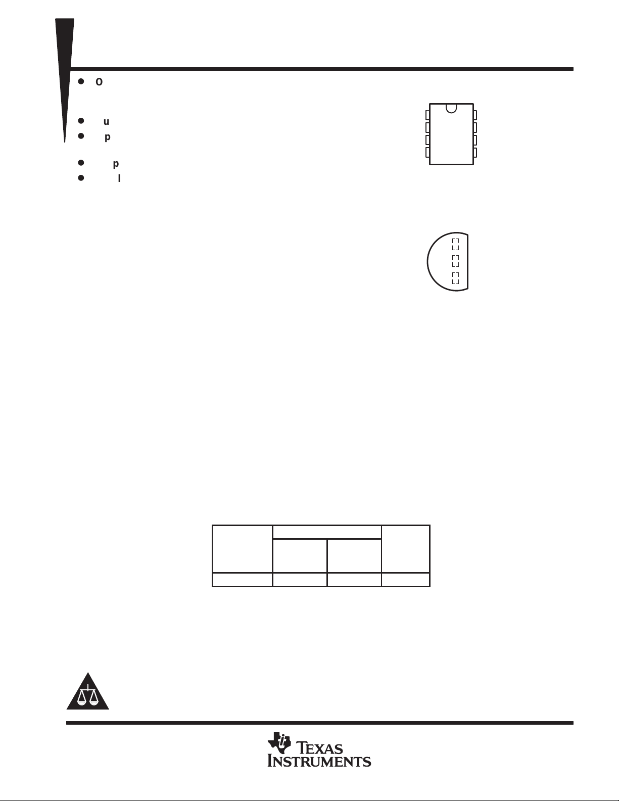
D PACKAGE
(TOP VIEW)
Resistor Divider
D
Output Current Capability of 100 mA
D
Input Regulation Typically 0.01% Per
Input-Voltage Change
D
Output Regulation Typically 0.5%
D
Ripple Rejection Typically 80 dB
description
The TL317 is an adjustable three-terminal
INPUT
OUTPUT
OUTPUT
ADJUSTMENT
NC – No internal connection
OUTPUT terminals are all internally connected.
1
2
3
4
LP PACKAGE
(TOP VIEW)
8
7
6
5
NC
OUTPUT
OUTPUT
NC
positive-voltage regulator capable of supplying
100 mA over an output-voltage range of 1.2 V to
32 V. It is exceptionally easy to use and requires
only two external resistors to set the output
voltage.
INPUT
OUTPUT
ADJUSTMENT
In addition to higher performance than fixed
regulators, this regulator offers full overload
protection available only in integrated circuits. Included on the chip are current-limiting and thermal-overload
protection. All overload-protection circuitry remains fully functional, even when ADJUSTMENT is disconnected.
Normally, no capacitors are needed unless the device is situated far from the input filter capacitors, in which
case an input bypass is needed. An optional output capacitor can be added to improve transient response.
ADJUSTMENT can be bypassed to achieve very high ripple rejection, which is difficult to achieve with standard
three-terminal regulators.
In addition to replacing fixed regulators, the TL317 regulator is useful in a wide variety of other applications.
Since the regulator is floating and sees only the input-to-output differential voltage, supplies of several hundred
volts can be regulated as long as the maximum input-to-output differential is not exceeded. Its primary
application is that of a programmable output regulator, but by connecting a fixed resistor between
ADJUSTMENT and OUTPUT , this device can be used as a precision current regulator . Supplies with electronic
shutdown can be achieved by clamping ADJUSTMENT to ground, programming the output to 1.2 V , where most
loads draw little current.
The TL317C is characterized for operation over the virtual junction temperature range of 0°C to 125°C.
AVAILABLE OPTIONS
PACKAGED DEVICES
T
J
0°C to 125°C TL317CD TL317CLP TL317Y
The D and LP packages are available taped and reeled. Add
the suffix R to device type (e.g., TL317CDR). Chip forms are
tested at 25°C.
Please be aware that an important notice concerning availability, standard warranty, and use in critical applications of
Texas Instruments semiconductor products and disclaimers thereto appears at the end of this data sheet.
SMALL
OUTLINE
(D)
PLASTIC
(LP)
FORM
(Y)
PRODUCTION DATA information is current as of publication date.
Products conform to specifications per the terms of Texas Instruments
standard warranty. Production processing does not necessarily include
testing of all parameters.
POST OFFICE BOX 655303 • DALLAS, TEXAS 75265
Copyright 1999, Texas Instruments Incorporated
1
TL317
3-TERMINAL ADJUSTABLE REGULATORS
SLVS004C – APRIL 1979 – REVISED JULY 1999
schematic
310 Ω 5.6 kΩ251 Ω190 Ω310 Ω
200 kΩ
124 Ω
11.5 kΩ
2.1 k
INPUT
Ω
360
Ω
1.4 Ω
30
pF
195
Ω
NOTE A: All component values shown are nominal.
5.3 kΩ 5.7 kΩ 70 Ω 5.1 kΩ
30
pF
absolute maximum ratings over operating temperature range (unless otherwise noted)
Input-to-output differential voltage, V
– VO 35 V. . . . . . . . . . . . . . . . . . . . . . . . . . . . . . . . . . . . . . . . . . . . . . . . . . . .
l
10.8 kΩ
2.12 kΩ
40 Ω
670 Ω
OUTPUT
ADJUSTMENT
†
Operating free-air, TA, case, or virtual-junction temperature range, TJ: TL317C 0°C to 150°C. . . . . . . . . . . .
Package thermal impedance, θJA (see Notes 1 and 2): D package 97°C/W. . . . . . . . . . . . . . . . . . . . . . . . . . . .
LP package 156°C/W. . . . . . . . . . . . . . . . . . . . . . . . . .
Lead temperature 1,6 mm (1/16 inch) from case for 10 seconds 260°C. . . . . . . . . . . . . . . . . . . . . . . . . . . . . . .
Storage temperature range, T
†
Stresses beyond those listed under “absolute maximum ratings” may cause permanent damage to the device. These are stress ratings only, and
functional operation of the device at these or any other conditions beyond those indicated under “recommended operating conditions” is not
implied. Exposure to absolute-maximum-rated conditions for extended periods may affect device reliability.
NOTES: 1. Maximum power dissipation is a function of TJ(max),
ambient temperature is PD = (TJ(max) – TA)/
2. The package thermal impedance is calculated in accordance with JESD 51, except for through-hole packages, which use a trace
length of zero.
–65°C to 150°C. . . . . . . . . . . . . . . . . . . . . . . . . . . . . . . . . . . . . . . . . . . . . . . . . . .
stg
θ
, and TA. The maximum allowable power dissipation at any allowable
θ
JA
JA
. Operating at the absolute maximum TJ of 150°C can impact reliability.
recommended operating conditions
Input-to-output voltage differential, VI – V
Output current, I
Operating virtual-junction temperature, T
2
O
O
J
POST OFFICE BOX 655303 • DALLAS, TEXAS 75265
MIN MAX UNIT
35 V
2.5 100 mA
TL317C 0 125 °C
PARAMETER
TEST CONDITIONS
†
UNIT
Input voltage regulation (see Note 3)
V
V
5 V to 35 V
%V
I
100 mA
Out ut voltage regulation
I
,
PARAMETER
TEST CONDITIONS
†
UNIT
Output voltage regulation
I
2.5 mA to 100 mA
TL317
3-TERMINAL ADJUSTABLE REGULATORS
SLVS004C – APRIL 1979 – REVISED JULY 1999
electrical characteristics over recommended operating virtual-junction temperature range (unless
otherwise noted)
TL317C
MIN TYP MAX
p
Ripple regulation
Output voltage regulation
Output voltage change with temperature TJ = 0°C to 125°C 10 mV/V
Output voltage long-term drift After 1000 hours at TJ = 125°C and VI – VO = 35 V 3 10 mV/V
Output noise voltage f = 10 Hz to 10 kHz, TJ = 25°C 30 µV/V
Minimum output current to maintain regulation VI – VO = 35 V 1.5 2.5 mA
Peak output current VI – VO ≤ 35 V 100 200 mA
ADJUSTMENT current 50 100 µA
Change in ADJUSTMENT current VI – VO = 2.5 V to 35 V, IO = 2.5 mA to 100 mA 0.2 5 µA
Reference voltage (output to ADJUSTMENT)
†
Unless otherwise noted, these specifications apply for the following test conditions: VI – VO = 5 V and IO = 40 mA. Pulse-testing techniques must
be used that maintain the junction temperature as close to the ambient temperature as possible. All characteristics are measured with a 0.1-µF
capacitor across the input and a 1-µF capacitor across the output.
NOTE 3: Input voltage regulation is expressed here as the percentage change in output voltage per 1-V change at the input.
–
=
I
O
VO = 10 V, f = 120 Hz 65
VO = 10 V,
10-µF capacitor between ADJUSTMENT and ground
VI = 5 V to 35 V,
= 2.5 mA to
O
TJ = 25°C
V
= 5 V to 35 V,
IO = 2.5 mA to 100 mA
VI – VO = 5 V to 35 V,
P ≤ rated dissipation
TJ = 25°C 0.01 0.02
IO = 2.5 mA to 100 mA 0.02 0.05
66 80
VO ≤ 5 V 25 mV
,
VO ≥ 5 V 5 mV/V
VO ≤ 5 V 50 mV
VO ≥ 5 V 10 mV/V
IO = 2.5 mA to 100 mA,
1.2 1.25 1.3 V
dB
electrical characteristics over recommended operating conditions, TJ = 25°C (unless otherwise
noted)
TL317Y
MIN TYP MAX
Input voltage regulation (see Note 3) VI – VO = 5 V to 35 V 0.01 %V
VO = 10 V, f = 120 Hz 65
Ripple regulation
p
Output noise voltage f = 10 Hz to 10 kHz 30 µV/V
Minimum output current to maintain regulation VI – VO = 35 V 1.5 mA
Peak output current VI – VO ≤ 35 V 200 mA
ADJUSTMENT current 50 µA
Change in ADJUSTMENT current VI – VO = 2.5 V to 35 V, IO = 2.5 mA to 100 mA 0.2 µA
Reference voltage (output to ADJUSTMENT)
†
Unless otherwise noted, these specifications apply for the following test conditions: VI – VO = 5 V and IO = 40 mA. Pulse-testing techniques must
be used that maintain the junction temperature as close to the ambient temperature as possible. All characteristics are measured with a 0.1-µF
capacitor across the input and a 1-µF capacitor across the output.
NOTE 3: Input voltage regulation is expressed here as the percentage change in output voltage per 1-V change at the input.
VO = 10 V,
10-µF capacitor between ADJUSTMENT and ground
=
O
VI – VO = 5 V to 35 V,
P ≤ rated dissipation
VO ≤ 5 V 25 mV
VO ≥ 5 V 5 mV/V
IO = 2.5 mA to 100 mA,
80
1.25 V
dB
POST OFFICE BOX 655303 • DALLAS, TEXAS 75265
3

TL317
3-TERMINAL ADJUSTABLE REGULATORS
SLVS004C – APRIL 1979 – REVISED JULY 1999
APPLICATION INFORMATION
TL317
V
I
C1 = 0.1 µF
(see Note A)
NOTES: A. Use of an input bypass capacitor is recommended if
regulator is far from the filter capacitors.
B. Output voltage is calculated from the equation:
V
O
where: V
ADJUSTMENT voltages (≈1.25 V).
C. Use of an output capacitor improves transient response
but is optional.
OutputInput
Adjustment
R2
ǒ
+
V
1
)
ref
R1
equals the difference between OUTPUT and
ref
R1
470 Ω
R2
Ǔ
V
O
(see Note B)
C2 = 1 µF
(see Note C)
Figure 1. Adjustable Voltage Regulator
TL317
V
V
I
C1 =
0.1 µF
Adjustment
R2 =
10 kΩ
OutputInput
R1 =
470 Ω
+
C2 = 10 µF
–
†
D1
1N4002
O
(see Note A)
+
C3 = 1 µF
–
TL317
35 V
C1 = 0.1 µF
NOTE A: Output voltage is calculated from the equation:
V
where: V
and ADJUSTMENT voltages (≈1.25 V).
ǒ
+
V
ref
O
equals the difference between OUTPUT
ref
OutputInput
Adjustment
–10 V
R3 =
820 Ω
1N4002
R2)R3
1
)
R1
Ǔ
*
V
(see Note A)
R1 = 120 Ω
R2 = 3 kΩ
10 V
O
Figure 2. 0-V to 30-V Regulator Circuit
†
D1 discharges C2 if output is shorted to ground.
NOTE A: Use of an output capacitor improves transient response but is
optional.
Figure 3. Regulator Circuit
With Improved Ripple Rejection
4
POST OFFICE BOX 655303 • DALLAS, TEXAS 75265
TL317
V
I
OutputInput
Adjustment
R1
I
limit
Figure 4. Precision Current-Limiter Circuit
+
1.25
R1

TL317
3-TERMINAL ADJUSTABLE REGULATORS
SLVS004C – APRIL 1979 – REVISED JULY 1999
APPLICATION INFORMATION
R2 = 1.5 kΩ
Adjustment
V
I
C1 = 0.1 µF
OutputInput
TL317
C2 = 1 µF
R1 = 470 Ω
TL317
Adjustment
OutputInput
Output
Adjust
V
R3 =
240 Ω
R4 =
2 kΩ
Figure 5. Tracking Preregulator Circuit
V
I
O
R2 = 5.1 kΩ
Figure 6. Slow Turnon 15-V Regulator Circuit
V
I
TL317
OutputInput
Adjustment
TL317
Adjustment
VO = 15 V
R1 =
470 Ω
R3 = 50 kΩ
2N2905
OutputInput
240 Ω
1N4002
C1 = 25 µF
TL317
V
I
OutputInput
Adjustment
24 Ω
Figure 7. 50-mA Constant-Current
Battery Charger Circuit
1.1 kΩ
R
+
V–
V
BE
Figure 8. Current-Limited 6-V Charger
V
I
CHG
BE
I
CHG
POST OFFICE BOX 655303 • DALLAS, TEXAS 75265
5

TL317
3-TERMINAL ADJUSTABLE REGULATORS
SLVS004C – APRIL 1979 – REVISED JULY 1999
APPLICATION INFORMATION
TIP73
V
I
22 Ω
10 µF
†
Minimum load current is 30 mA.
‡
Optional capacitor improves ripple rejection
2N2905
5 kΩ
TL317
OutputInput
Adjustment
5 kΩ
500 Ω
120 Ω
10 µF
‡
1N4002
R
†
L
Figure 9. High-Current Adjustable Regulator
V
O
47 µF
6
POST OFFICE BOX 655303 • DALLAS, TEXAS 75265

IMPORTANT NOTICE
T exas Instruments and its subsidiaries (TI) reserve the right to make changes to their products or to discontinue
any product or service without notice, and advise customers to obtain the latest version of relevant information
to verify, before placing orders, that information being relied on is current and complete. All products are sold
subject to the terms and conditions of sale supplied at the time of order acknowledgement, including those
pertaining to warranty, patent infringement, and limitation of liability.
TI warrants performance of its semiconductor products to the specifications applicable at the time of sale in
accordance with TI’s standard warranty. Testing and other quality control techniques are utilized to the extent
TI deems necessary to support this warranty . Specific testing of all parameters of each device is not necessarily
performed, except those mandated by government requirements.
CERTAIN APPLICA TIONS USING SEMICONDUCT OR PRODUCTS MAY INVOLVE POTENTIAL RISKS OF
DEATH, PERSONAL INJURY, OR SEVERE PROPERTY OR ENVIRONMENTAL DAMAGE (“CRITICAL
APPLICATIONS”). TI SEMICONDUCTOR PRODUCTS ARE NOT DESIGNED, AUTHORIZED, OR
WARRANTED TO BE SUITABLE FOR USE IN LIFE-SUPPORT DEVICES OR SYSTEMS OR OTHER
CRITICAL APPLICA TIONS. INCLUSION OF TI PRODUCTS IN SUCH APPLICATIONS IS UNDERST OOD TO
BE FULLY AT THE CUSTOMER’S RISK.
In order to minimize risks associated with the customer’s applications, adequate design and operating
safeguards must be provided by the customer to minimize inherent or procedural hazards.
TI assumes no liability for applications assistance or customer product design. TI does not warrant or represent
that any license, either express or implied, is granted under any patent right, copyright, mask work right, or other
intellectual property right of TI covering or relating to any combination, machine, or process in which such
semiconductor products or services might be or are used. TI’s publication of information regarding any third
party’s products or services does not constitute TI’s approval, warranty or endorsement thereof.
Copyright 1999, Texas Instruments Incorporated
 Loading...