

Page 1

查询TL16C554A供应商
D
Integrated Asynchronous-Communications
Element
D
Consists of Four Improved TL16C550C
ACEs Plus Steering Logic
D
In FIFO Mode, Each ACE Transmitter and
Receiver Is Buffered With 16-Byte FIFO to
Reduce the Number of Interrupts to CPU
D
In TL16C450 Mode, Hold and Shift
Registers Eliminate Need for Precise
Synchronization Between the CPU and
Serial Data
D
Up to 16-MHz Clock Rate for up to 1-Mbaud
Operation
D
Programmable Baud-Rate Generators
Which Allow Division of Any Input
Reference Clock by 1 to (2
Generate an Internal 16 × Clock
D
Adds or Deletes Standard Asynchronous
Communication Bits (Start, Stop, and
Parity) to or From the Serial-Data Stream
D
Independently Controlled Transmit,
Receive, Line Status, and Data Set
Interrupts
D
5-V and 3.3-V Operation
description
16
–1) and
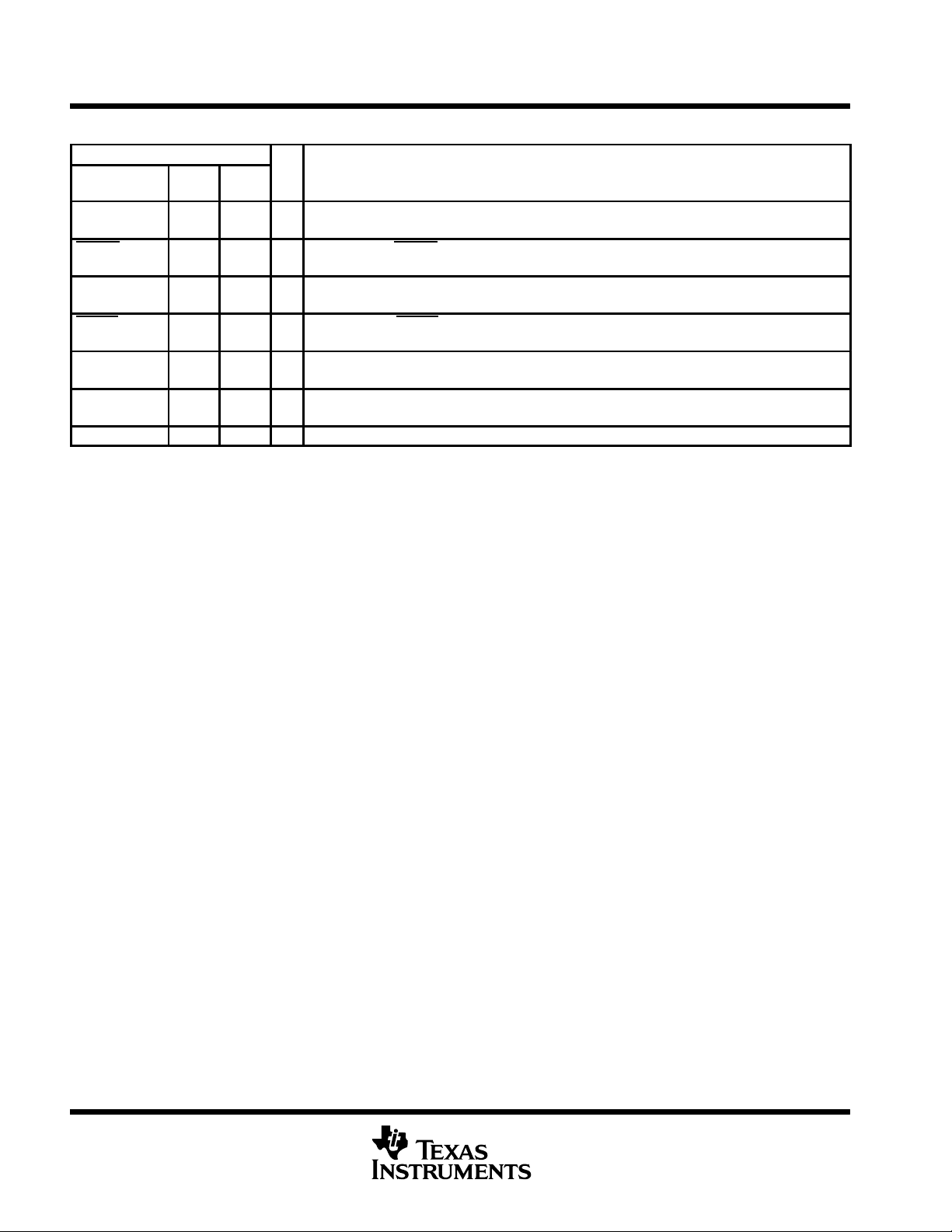
TL16C554A, TL16C554AI
ASYNCHRONOUS-COMMUNICATIONS ELEMENT
SLLS509A – AUGUST 2001 – REVISED JUL Y 2003
D
Fully Programmable Serial Interface
Characteristics:
– 5-, 6-, 7-, or 8-Bit Characters
– Even-, Odd-, or No-Parity Bit
– 1-, 1 1/2-, or 2-Stop Bit Generation
– Baud Generation (DC to 1-Mbit Per
Second)
D
False Start Bit Detection
D
Complete Status Reporting Capabilities
D
Line Break Generation and Detection
D
Internal Diagnostic Capabilities:
– Loopback Controls for Communications
Link Fault Isolation
– Break, Parity, Overrun, Framing Error
Simulation
D
Fully Prioritized Interrupt System Controls
D
Modem Control Functions (CTS, RTS, DSR,
DTR
, RI, and DCD)
D
3-State Outputs Provide TTL Drive
Capabilities for Bidirectional Data Bus and
Control Bus
D
Programmable Auto-RTS and Auto-CTS
D
CTS Controls Transmitter in Auto-CTS
Mode,
D
RCV FIFO Contents and Threshold Control
RTS
in Auto-RTS Mode,
The TL16C554A is an enhanced quadruple version of the TL16C550C asynchronous-communications element
(ACE). Each channel performs serial-to-parallel conversion on data characters received from peripheral
devices or modems and parallel-to-serial conversion on data characters transmitted by the CPU. The complete
status of each channel of the quadruple ACE can be read by the CPU at any time during operation. The
information obtained includes the type and condition of the operation performed and any error conditions
encountered.
The TL16C554A quadruple ACE can be placed in an alternate FIFO mode, which activates the internal FIFOs
to allow 16 bytes (plus three bits of error data per byte in the receiver FIFO) to be stored in both receive and
transmit modes. In the FIFO mode of operation, there is a selectable autoflow control feature that can
significantly reduce software overhead and increase system efficiency by automatically controlling serial-data
flow using RTS
system efficiency . T wo terminal functions allow signaling of direct-memory access (DMA) transfers. Each ACE
includes a programmable baud-rate generator that can divide the timing reference clock input by a divisor
between 1 and 2
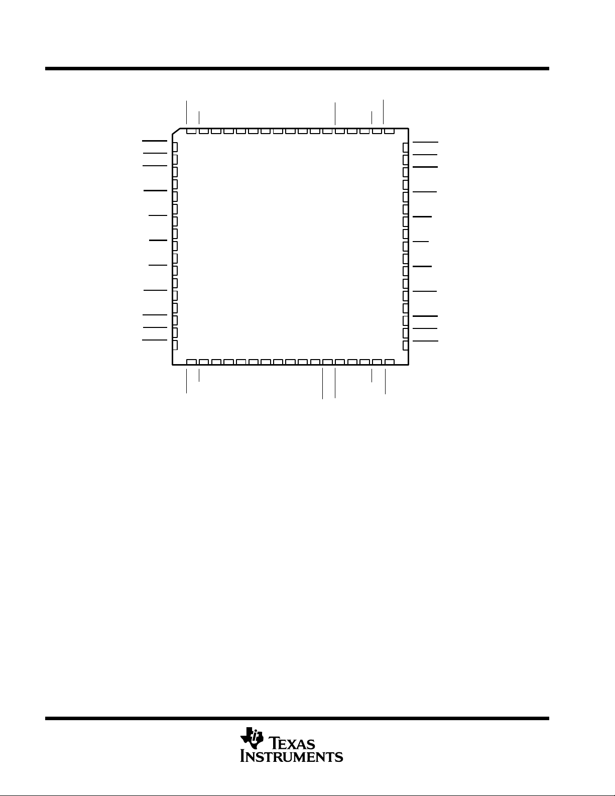
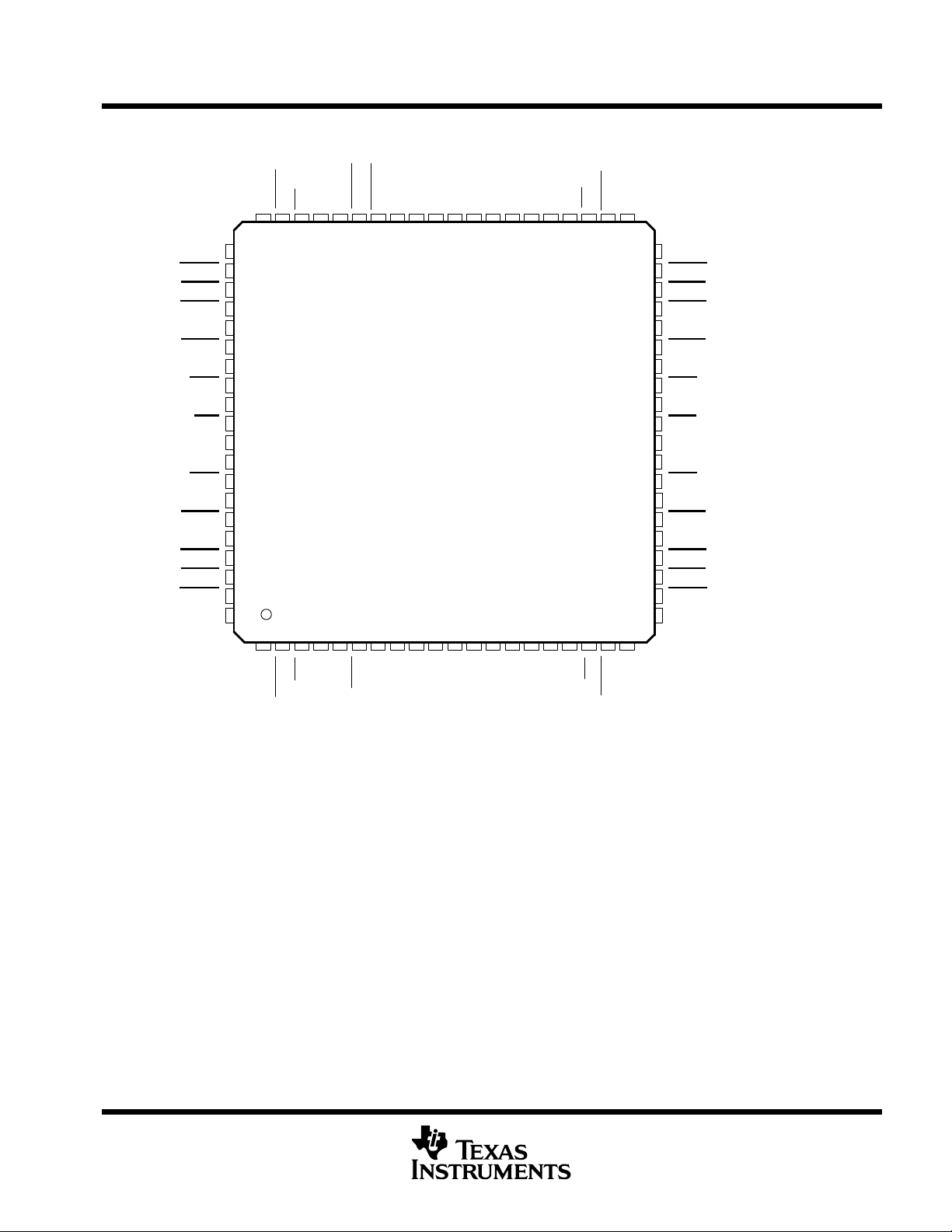
The TL16C554A is available in a 68-pin plastic-leaded chip-carrier (PLCC) FN package and in an 80-pin (TQFP)
PN package.
Please be aware that an important notice concerning availability, standard warranty, and use in critical applications of
Texas Instruments semiconductor products and disclaimers thereto appears at the end of this data sheet.
PRODUCTION DATA information is current as of publication date.
Products conform to specifications per the terms of Texas Instruments
standard warranty. Production processing does not necessarily include
testing of all parameters.
output and CTS input signals. All logic is on the chip to minimize system overhead and maximize
16
–1.
Copyright 2001 – 2003, Texas Instruments Incorporated
POST OFFICE BOX 655303 • DALLAS, TEXAS 75265
1
Page 2
TL16C554A, TL16C554AI
ASYNCHRONOUS-COMMUNICATIONS ELEMENT
SLLS509A – AUGUST 2001 – REVISED JULY 2003
FN PACKAGE
(TOP VIEW)
RXA
DCDA
RIA
GNDD7D6D5D4
D3
D2
D1
D0
V
INTN
CC
RXD
RID
DCDD
DSRA
CTSA
DTRA
V
CC
RTSA
INTA
CSA
TXA
IOW
TXB
CSB
INTB
RTSB
GND
DTRB
CTSB
DSRB
NC – No internal connection
87 65493
10
11
12
13
14
15
16
17
18
19
20
21
22
23
24
25
26
27
DCDB
28 29
RIB
30
RXB
CC
V
31 32 33 34
A2A1A0
NC
168672
35 36 37 38 39
XTAL1
XTAL2
66 65
RESET
RXRDY
64 63 62 61
40 41 42 43
RXC
GND
TXRDY
RIC
60
59
58
57
56
55
54
53
52
51
50
49
48
47
46
45
44
DCDC
DSRD
CTSD
DTRD
GND
RTSD
INTD
CSD
TXD
IOR
TXC
CSC
INTC
RTSC
V
CC
DTRC
CTSC
DSRC
2
POST OFFICE BOX 655303 • DALLAS, TEXAS 75265
Page 3
ASYNCHRONOUS-COMMUNICATIONS ELEMENT
PN PACKAGE
(TOP VIEW)
TL16C554A, TL16C554AI
SLLS509A – AUGUST 2001 – REVISED JULY 2003
NC
DSRC
CTSC
DTRC
V
CC
RTSC
INTC
CSC
TXC
IOR
NC
TXD
CSD
INTD
RTSD
GND
DTRD
CTSD
DSRD
NC
NC
DCDC
59 58 57 56 5560 54
61
62
63
64
65
66
67
68
69
70
71
72
73
74
75
76
77
78
79
80
23
1
RIC
RXC
5678
4
GND
TXRDY
RXRDY
RESET
NC
52 51 5053
9
10 11 12 13
XTAL2
XTAL1
49 48
NC
A0
47 46 45 44
14 15 16 17
A1
A2
V
CC
RXB
RIB
43 42 41
18 19 20
NC
DCDB
40
39
38
37
36
35
34
33
32
31
30
29
28
27
26
25
24
23
22
21
NC
DSRB
CTSB
DTRB
GND
RTSB
INTB
CSB
TXB
IOW
NC
TXA
CSA
INTA
RTSA
V
CC
DTRA
CTSA
DSRA
NC
NC
RID
DCDD
NC – No internal connection
RXD
V
CC
D0D1D2
INTN
NC
D3
D4
D5
D6
D7
GND
RXA
RIA
NC
DCDA
POST OFFICE BOX 655303 • DALLAS, TEXAS 75265
3
Page 4
TL16C554A, TL16C554AI
ASYNCHRONOUS-COMMUNICATIONS ELEMENT
SLLS509A – AUGUST 2001 – REVISED JULY 2003
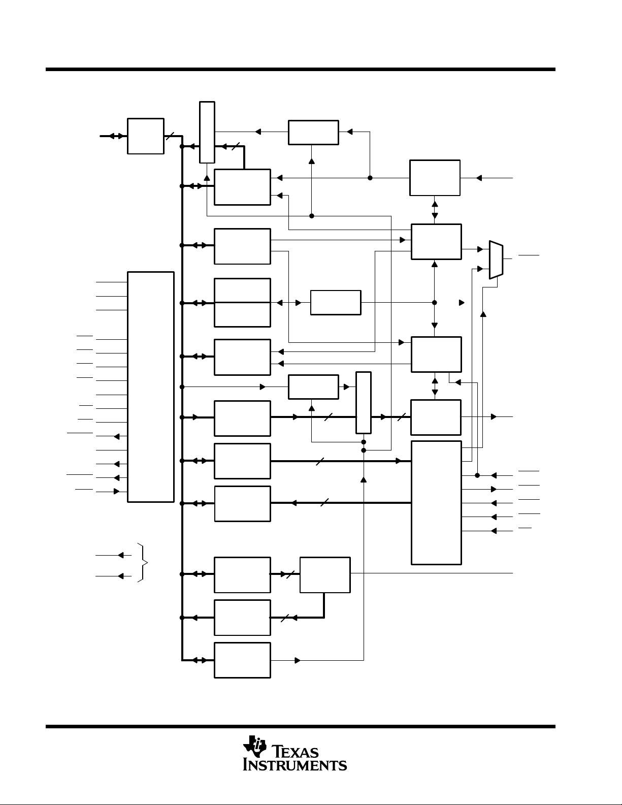
functional block diagram (per channel)
D(7–0)
A0
A1
A2
CSA
CSB
CSC
CSD
RESET
IOR
IOW
TXRDY
XTAL1
XTAL2
RXRDY
INTN
V
CC
GND
5 – 66
34
33
32
16
20
50
54
37
52
18
39
35
36
38
65
13, 30, 47, 64
6, 23, 40, 57
Data
Bus
Buffer
Select
and
Control
Logic
Internal
8
Power
Supply
Data
Bus
S
e
l
e
c
t
8
Receiver
Buffer
Register
Line
Control
Register
Divisor
Latch (LS)
Divisor
Latch (MS)
Line
Status
Register
Transmitter
Holding
Register
Modem
Control
Register
Modem
Status
Register
Interrupt
Enable
Register
Receiver
FIFO
Transmitter
FIFO
Interrupt
8
Control
Logic
Baud
Generator
8
8
8
Receiver
Shift
Register
Receiver
Timing and
Control
Transmitter
Timing and
Control
S
e
l
e
c
t
Transmitter
8
Shift
Register
Modem
Control
Logic
7
14
Autoflow
Control
(AFE)
17
11
12
10
9
8
15
RXA
RTSA
TXA
CTSA
DTRA
DSRA
DCDA
RIA
INTA
Interrupt
Identification
Register
FIFO
Control
Register
8
NOTE A: Terminal numbers shown are for the FN package and channel A.
4
POST OFFICE BOX 655303 • DALLAS, TEXAS 75265
Page 5
TL16C554A, TL16C554AI
ASYNCHRONOUS-COMMUNICATIONS ELEMENT
SLLS509A – AUGUST 2001 – REVISED JULY 2003
Terminal Functions
TERMINAL
NAME
A0
A1
A2
CSA, CSB,
CSC
, CSD
CTSA, CTSB,
CTSC
, CTSD
D7–D0 66–68
DCDA, DCDB,
DCDC
, DCDD
DSRA, DSRB,
DSRC
, DSRD
DTRA, DTRB,
DTRC
, DTRD
GND 6, 23,
INTN
INTA, INTB,
INTC, INTD
IOR 52 70 I Read strobe. A low level on IOR transfers the contents of the selected register to the external CPU
IOW 18 31 I Write strobe. IOW allows the the CPU to write to the register selected by the address.
RESET 37 53 I Master reset. When active, RESET clears most ACE registers and sets the state of various signals.
RIA, RIB,
RIC
, RID
RTSA, RTSB,
RTSC
, RTSD
FN
NO.PNNO.
34
33
32
16, 20,
50, 54
11, 25,
45, 59
43, 61
10, 26,
44, 60
12, 24,
46, 58
40, 57
15, 21,
49, 55
42, 62
14, 22,
48, 56
28, 33,
68, 73
23, 38,
63, 78
15–11,
1–5
9, 27,
19,42,
59, 2
22, 39,
62, 79
24, 37,
64, 77
16, 36,
56, 76
65 6 I
27, 34,
67, 74
8, 28,
18, 43,
58, 3
26, 35,
66, 75
I/O DESCRIPTION
48
47
46
9–7
I Register select terminals. A0, A1, and A2 are three inputs used during read and write operations to
select the ACE register to read or write.
I Chip select. Each chip select (CSx) enables read and write operations to its respective channel.
I Clear to send. CTS is a modem status signal. Its condition can be checked by reading bit 4 (CTS)
of the modem-status register. Bit 0 (∆CTS) of the modem-status register indicates that CTS
changed state since the last read from the modem-status register. If the modem-status interrupt is
enabled when CTS changes levels and the auto-CTS mode is not enabled, an interrupt is generated.
CTS
is also used in the auto-CTS mode to control the transmitter.
I/O Data bus. Eight data lines with 3-state outputs provide a bidirectional path for data, control, and status
information between the TL16C554A and the CPU. D0 is the least-significant bit (LSB).
I Data carrier detect. A low on DCDx indicates the carrier has been detected by the modem. The
condition of this signal is checked by reading bit 7 of the modem-status register.
Data set ready. DSRx is a modem-status signal. Its condition can be checked by reading bit 5 (DSR)
I
of the modem-status register. DSR
O Data terminal ready. DTRx is an output that indicates to a modem or data set that the ACE is ready
to establish communications. It is placed in the active state by setting the DTR bit of the modemcontrol register. DTRx
loop-mode operation, or when clearing bit 0 (DTR
Signal and power ground
Interrupt normal. INTN operates in conjunction with bit 3 of the modem-status register and affects
operation of the interrupts (INTA, INTB, INTC, and INTD) for the four universal asynchronous
receiver/transceivers (UARTs) per the following table.
INTN OPERATION OF INTERRUPTS
Brought low or
allowed to float
Brought high Interrupts are always enabled, overriding the OUT2 enables.
O External interrupt output. The INTx outputs go high (when enabled by the interrupt register) and
inform the CPU that the ACE has an interrupt to be serviced. Four conditions that cause an interrupt
to be issued are: receiver error, receiver data available or timeout (FIFO mode only), transmitter
holding register empty , and an enabled modem-status interrupt. The interrupt is disabled when it is
serviced or as the result of a master reset.
bus.
The transmitter output and the receiver input are disabled during reset time.
I Ring detect indicator . A low on RIx indicates the modem has received a ring signal from the telephone
line. The condition of this signal can be checked by reading bit 6 of the modem-status register.
O Request to send. When active, RTS informs the modem or data set that the ACE is ready to receive
data. RTS
inactive (high) level either as a result of a master reset, or during loop-mode operations, or by clearing
bit 1 (RTS) of the MCR. In the auto-RTS mode, RTS is set to the inactive level by the receiver
threshold-control logic.
is set to the active level by setting the RTS modem-control register bit, and is set to the
is placed in the inactive state (high) either as a result of the master reset during
Interrupts are enabled according to the state of OUT2 (MCR bit 3). When the MCR
bit 3 is cleared, the 3-state interrupt output of that UART is in the high-impedance
state. When the MCR bit 3 is set, the interrupt output of the UART is enabled.
has no effect on the transmit or receive operation.
) of the modem-control register.
has
POST OFFICE BOX 655303 • DALLAS, TEXAS 75265
5
Page 6
TL16C554A, TL16C554AI
ASYNCHRONOUS-COMMUNICATIONS ELEMENT
SLLS509A – AUGUST 2001 – REVISED JULY 2003
Terminal Functions (Continued)
TERMINAL
NAME
RXA, RXB
RXC, RXD
RXRDY 38 54 O Receive ready. RXRDY goes low when the receive FIFO is full. It can be used as a single transfer
TXA, TXB
TXC, TXD
TXRDY 39 55 O T ransmit ready. TXRDY goes low when the transmit FIFO is full. It can be used as a single transfer
V
CC
XTAL1 35 50 I Crystal input 1 or external clock input. A crystal can be connected to XTAL1 and XT AL2 to utilize the
XTAL2 36 51 O Crystal output 2 or buffered clock output (see XT AL1).
FN
NO.PNNO.
7, 29,
41, 63
17, 19,
51, 53
13, 30,
47, 64
17, 44,
29, 32,
69, 72
5, 25,
45, 65
57, 4
I/O DESCRIPTION
I Serial input. RXx is a serial-data input from a connected communications device. During loopback
mode, the RXx input is disabled from external connection and connected to the TXx output internally .
or multitransfer.
O Transmit outputs. TXx is a composite serial-data output connected to a communications device.
TXA, TXB, TXC, and TXD are set to the marking (high) state as a result of reset.
or multitransfer function.
Power supply
internal oscillator circuit. An external clock can be connected to drive the internal-clock circuits.
absolute maximum ratings over free-air temperature range (unless otherwise noted)
Supply voltage range, V
Input voltage range at any input, V
Output voltage range, V
(see Note 1) –0.5 V to 7 V. . . . . . . . . . . . . . . . . . . . . . . . . . . . . . . . . . . . . . . . . . . . . .
CC
–0.5 V to VCC + 3 V. . . . . . . . . . . . . . . . . . . . . . . . . . . . . . . . . . . . . . . . . . . . . . . . . . . . .
O
–0.5 V to 7 V. . . . . . . . . . . . . . . . . . . . . . . . . . . . . . . . . . . . . . . . . . . . . . . . . . .
I
†
Continuous total-power dissipation at (or below) 70°C 500 mW. . . . . . . . . . . . . . . . . . . . . . . . . . . . . . . . . . . . . . .
Operating free-air temperature range, T
: TL16C554A 0°C to 70°C. . . . . . . . . . . . . . . . . . . . . . . . . . . . . . . . . .
A
TL16C554AI –40°C to 85°C. . . . . . . . . . . . . . . . . . . . . . . . . . . . . . .
Storage temperature range, T
†
Stresses beyond those listed under “absolute maximum ratings” may cause permanent damage to the device. These are stress ratings only, and
functional operation of the device at these or any other conditions beyond those indicated under “recommended operating conditions” is not
implied. Exposure to absolute-maximum-rated conditions for extended periods may affect device reliability.
NOTE 1: All voltage levels are with respect to GND.
–65°C to 150°C. . . . . . . . . . . . . . . . . . . . . . . . . . . . . . . . . . . . . . . . . . . . . . . . . . .
stg
6
POST OFFICE BOX 655303 • DALLAS, TEXAS 75265
Page 7
TL16C554A, TL16C554AI
O erating free-air tem erature, T
A
CC SS
g
ASYNCHRONOUS-COMMUNICATIONS ELEMENT
SLLS509A – AUGUST 2001 – REVISED JULY 2003
recommended operating conditions, standard voltage (5 V-nominal)
MIN NOM MAX UNIT
Supply voltage, V
Clock high-level input voltage at XTAL1, V
Clock low-level input voltage at XTAL1, V
High-level input voltage, V
Low-level input voltage, V
Clock frequency, f
p
CC
clock
IH(CLK)
IL(CLK)
IH
IL
p
TL16C554A 0 70 °C
TL16C554AI –40 85 °C
electrical characteristics over recommended ranges of operating free-air temperature and supply
voltage, standard voltage (5-V nominal) (unless otherwise noted)
PARAMETER TEST CONDITIONS MIN TYP†MAX UNIT
‡
V
OH
‡
V
OL
I
Ikg
I
OZ
I
CC
C
i(XTAL1)
C
o(XTAL2)
C
i
C
o
†
All typical values are at VCC = 5 V, TA = 25°C.
‡
These parameters apply for all outputs except XTAL2.
High-level output voltage IOH = –1 mA 2.4 V
Low-level output voltage IOL = 1.6 mA 0.4 V
Input leakage current
High-impedance output
current
Supply current
Clock input capacitance 15 20 pF
Clock output capacitance
Input capacitance
Output capacitance 10 20 pF
VCC = 5.25 V, GND = 0,
VI = 0 to 5.25 V, All other terminals floating
VCC = 5.25 V, GND = 0, VO = 0 to 5.25 V,
Chip selected in write mode or chip deselected
VCC = 5.25 V, TA = 25°C,
RX, DSR
All other inputs at 0.8 V , XTAL1 at 4 MHz,
No load on outputs, Baud rate = 50 kilobits per second
VCC = 0, VSS = 0, all other terminals grounded,
f = 1 MHz, TA = 25°C
, DCD, CTS, and RI at 2 V,
4.75 5 5.25 V
2 V
–0.5 0.8 V
2 V
–0.5 0.8 V
CC
CC
16 MHz
±10 µA
±20 µA
50 mA
20 30 pF
6 10 pF
V
V
POST OFFICE BOX 655303 • DALLAS, TEXAS 75265
7
Page 8
TL16C554A, TL16C554AI
O erating free-air tem erature, T
A
CC SS
g
ASYNCHRONOUS-COMMUNICATIONS ELEMENT
SLLS509A – AUGUST 2001 – REVISED JULY 2003
recommended operating conditions, low voltage (3.3-V nominal)
MIN NOM MAX UNIT
Supply voltage, V
Clock high-level input voltage at XTAL1, V
Clock low-level input voltage at XTAL1, V
High-level input voltage, V
Low-level input voltage, V
Clock frequency, f
p
CC
clock
IH(CLK)
IL(CLK)
IH
IL
p
TL16C554A 0 70 °C
TL16C554AI –40 85 °C
electrical characteristics over recommended ranges of operating free-air temperature and supply
voltage, low voltage (3.3-V nominal) (unless otherwise noted)
PARAMETER TEST CONDITIONS MIN TYP†MAX UNIT
‡
V
OH
‡
V
OL
I
Ikg
I
OZ
I
CC
C
i(XTAL1)
C
o(XTAL2)
C
i
C
o
†
All typical values are at VCC = 3.3 V, TA = 25°C.
‡
These parameters apply for all outputs except XTAL2.
High-level output voltage IOH = –1 mA 2.4 V
Low-level output voltage IOL = 1.6 mA 0.4 V
Input leakage current
High-impedance output
current
Supply current
Clock input capacitance 15 20 pF
Clock output capacitance
Input capacitance
Output capacitance 10 20 pF
VCC = 3.6 V, GND = 0,
VI = 0 to 3.6 V, All other terminals floating
VCC = 3.6 V, GND = 0, VO = 0 to 3.6 V,
Chip selected in write mode or chip deselected
VCC = 3.6 V, TA = 25°C,
RX, DSR
All other inputs at 0.8 V , XTAL1 at 4 MHz,
No load on outputs, Baud rate = 50 kilobits per second
VCC = 0, VSS = 0, all other terminals grounded,
f = 1 MHz, TA = 25°C
, DCD, CTS, and RI at 2 V,
3 3.3 3.6 V
2 V
–0.5 0.8 V
2 V
–0.5 0.8 V
CC
CC
16 MHz
±10 µA
±20 µA
40 mA
20 30 pF
6 10 pF
V
V
clock timing requirements over recommended ranges of operating free-air temperature and supply
voltage (see Figure 1)
t
w1
t
w2
t
w3
8
Pulse duration, clock high (external clock) 31 ns
Pulse duration, clock low (external clock) 31 ns
Pulse duration, RESET 1000 ns
MIN MAX UNIT
POST OFFICE BOX 655303 • DALLAS, TEXAS 75265
Page 9
TL16C554A, TL16C554AI
ASYNCHRONOUS-COMMUNICATIONS ELEMENT
SLLS509A – AUGUST 2001 – REVISED JULY 2003
read cycle timing requirements over recommended ranges of operating free-air temperature and
supply voltage (see Figure 4)
MIN MAX UNIT
t
w4
t
su1
t
su2
t
h1
t
h2
t
d1
t
d2
NOTES: 2. The internal address strobe is always active.
write cycle timing requirements over recommended ranges of operating free-air temperature and
supply voltage (see Figure 5)
t
w5
t
su3
t
su4
t
su5
t
h3
t
h4
t
h5
t
d3
t
d4
NOTE 2: The internal address strobe is always active.
Pulse duration, IOR low 75 ns
Setup time, CSx valid before IOR low (see Note 2) 10 ns
Setup time, A2–A0 valid before IOR low (see Note 2) 15 ns
Hold time, A2–A0 valid after IOR high (see Note 2) 0 ns
Hold time, CSx valid after IOR high (see Note 2) 0 ns
Delay time, t
Delay time, IOR high to IOR or IOW low 50 ns
3. In the FIFO mode, td1 = 425 ns (min) between reads of the receiver FIFO and the status registers (interrupt-identification register
and line-status register).
Pulse duration, IOW↓ 50 ns
Setup time, CSx valid before IOW↓ (see Note 2) 10 ns
Setup time, A2–A0 valid before IOW↓ (see Note 2) 15 ns
Setup time, D7–D0 valid before IOW↑ 10 ns
Hold time, A2–A0 valid after IOW↑ (see Note 2) 5 ns
Hold time, CSx valid after IOW↑ (see Note 2) 5 ns
Hold time, D7–D0 valid after IOW↑ 25 ns
Delay time, t
Delay time, IOW↑ to IOW or IOR↓ 55 ns
+ tw4 + td2 (see Note 3) 140 ns
su2
MIN MAX UNIT
su4
+ tw5 + t
d4
120 ns
read cycle switching characteristics over recommended ranges of operating free-air temperature
and supply voltage, CL = 100 pF (see Note 4 and Figure 4)
PARAMETER MIN MAX UNIT
t
Enable time, IOR↓ to D7–D0 valid 30 ns
en
t
Disable time, IOR↑ to D7–D0 released 0 20 ns
dis
NOTE 4: VOL and VOH (and the external loading) determine the charge and discharge time.
POST OFFICE BOX 655303 • DALLAS, TEXAS 75265
9
Page 10
TL16C554A, TL16C554AI
ASYNCHRONOUS-COMMUNICATIONS ELEMENT
SLLS509A – AUGUST 2001 – REVISED JULY 2003
transmitter switching characteristics over recommended ranges of operating free-air temperature
and supply voltage (see Figures 6, 7, and 8)
PARAMETER TEST CONDITIONS MIN MAX UNIT
t
Delay time, INTx↓ to TXx↓ at start See Note 7 8 24
d5
t
Delay time, TXx↓ at start to INTx↑ See Note 5 8 8
d6
t
Delay time, IOW high or low (WR THR) to INTx↑ See Note 5 16 32
d7
t
Delay time, TXx↓ at start to TXRDY↓ CL = 100 pF 8
d8
t
Propagation delay time, IOW (WR THR)↓ to INTx↓ CL = 100 pF 35 ns
pd1
t
Propagation delay time, IOR (RD IIR)↑ to INTx↓ CL = 100 pF 30 ns
pd2
t
Propagation delay time, IOW (WR THR)↑ to TXRDY↑ CL = 100 pF 50 ns
pd3
NOTE 5: If the transmitter interrupt delay is active, this delay is lengthened by one character time minus the last stop-bit time.
receiver switching characteristics over recommended ranges of operating free-air temperature
and supply voltage (see Figures 9 through 13)
PARAMETER TEST CONDITIONS MIN MAX UNIT
t
Delay time, stop bit to INTx↑ or stop bit to RXRDY↓ or read RBR to set interrupt See Note 6 1
d9
t
Propagation delay time, Read RBR/LSR to INTx↓/LSR interrupt↓
pd4
t
Propagation delay time, IOR RCLK↓ to RXRDY↑ See Note 7 30 ns
pd5
NOTES: 6. The receiver data available indicator, the overrun error indicator, the trigger level interrupts, and the active RXRDY indicator are
delayed three RCLK (internal receiver timing clock) cycles in the FIFO mode (FCR0 = 1). After the first byte has been received, status
indicators (PE, FE, BI) are delayed three RCLK cycles. These indicators are updated immediately for any further bytes received after
IOR
goes active for a read from the RBR register. There are eight RCLK cycle delays for trigger change level interrupts.
7. RCLK and baudout are internal signals derived from divisor latches LSB (DLL) and MSB (DLM) and input clock.
CL = 100 pF,
See Note 7
RCLK
cycles
RCLK
cycles
RCLK
cycles
RCLK
cycles
RCLK
cycle
40 ns
modem control switching characteristics over recommended ranges of operating free-air
temperature and supply voltage, C
t
Propagation delay time, IOW (WR MCR)↑ to RTSx, DTRx↑
pd6
t
Propagation delay time, modem input CTSx, DSRx, and DCDx ↓↑ to INTx↑ 30 ns
pd7
t
Propagation delay time, IOR (RD MSR)↑ to interrupt↓ 35 ns
pd8
t
Propagation delay time, RIx↑ to INTx↑ 30 ns
pd9
t
Propagation delay time, CTS low to SOUT↓ (See Note 7) 24
pd10
t
Setup time CTS high to midpoint of Tx stop bit 2
su6
t
Propagation delay time, RCV threshold byte to RTS↑ 2
pd11
t
Propagation delay time, IOR (RD RBR) low (read of last byte in receive FIFO) to RTS↓ 2
pd12
t
Propagation delay time, first data bit of 16th character to RTS↑ 2
pd13
t
Propagation delay time, IOR (RD RBR) low to RTS↓ 2
pd14
7. RCLK and baudout are internal signals derived from divisor latches LSB (DLL) and MSB (DLM) and input clock.
= 100 pF (see Figures 14, 15, 16, and 17)
L
PARAMETER MIN MAX UNIT
50 ns
baudout
cycles
baudout
cycles
baudout
cycles
baudout
cycles
baudout
cycles
baudout
cycles
10
POST OFFICE BOX 655303 • DALLAS, TEXAS 75265
Page 11
ASYNCHRONOUS-COMMUNICATIONS ELEMENT
SLLS509A – AUGUST 2001 – REVISED JULY 2003
PARAMETER MEASUREMENT INFORMATION
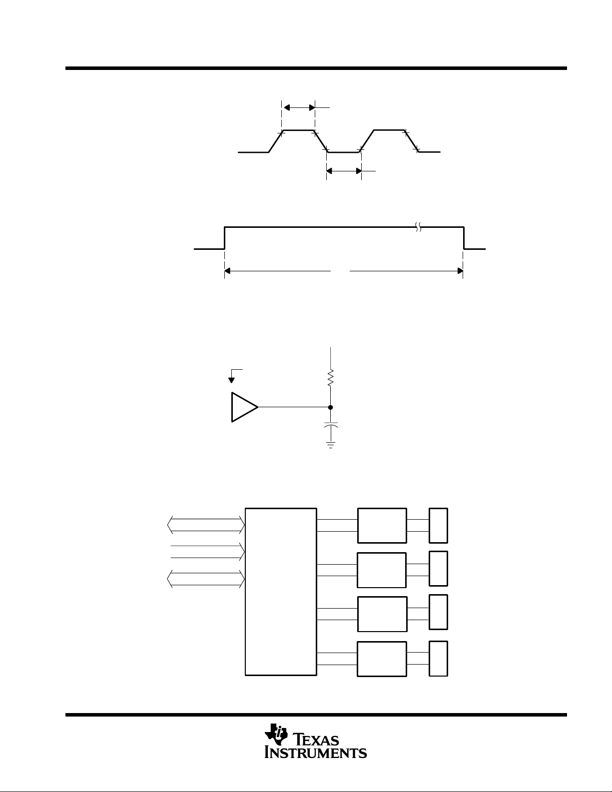
t
w1
TL16C554A, TL16C554AI
0.8 V
2 V2 V
f
= 16 MHz MAX
clock
t
w3
0.8 V
Clock
(XTAL1)
(a) CLOCK INPUT VOLTAGE WAVEFORM
RESET
(b) RESET VOLTAGE WAVEFORM
Figure 1. Clock Input and RESET Voltage Waveforms
2.54 V
Device Under Test
TL16C554
680 Ω
82 pF
(see Note A)
2 V
0.8 V
t
w2
Data Bus
Address Bus
Control Bus
NOTE A: This includes scope and jig capacitance.
Figure 2. Output Load Circuit
Serial
Channel 1
Buffers
Serial
TL16C554A
Quadruple
ACE
Channel 2
Buffers
Serial
Channel 3
Buffers
Serial
Channel 4
Buffers
Figure 3. Basic Test Configuration
9-Pin D Connector
9-Pin D Connector
9-Pin D Connector
9-Pin D Connector
POST OFFICE BOX 655303 • DALLAS, TEXAS 75265
11
Page 12
TL16C554A, TL16C554AI
ASYNCHRONOUS-COMMUNICATIONS ELEMENT
SLLS509A – AUGUST 2001 – REVISED JULY 2003
PARAMETER MEASUREMENT INFORMATION
A2, A1, A0
CSx
IOR
IOW
D7–D0
50%
50%
Valid
Valid
t
su1
t
t
su2
50%
t
en
d1
Active
t
w4
Valid Data
Figure 4. Read Cycle Timing Waveforms
t
50%
h1
t
h2
50%
t
dis
50%
t
d2
50%
50%
Active
or
Active
A2, A1, A0
CSx
IOW
IOR
D7–D0
50%
50%
Valid
Valid
t
t
su3
su4
50%
t
su5
t
Active
t
w5
d3
Valid Data
Figure 5. Write Cycle Timing Waveforms
t
h3
50%
50%
50%
t
h4
50%
t
d4
50%
t
h5
Active
or
Active
12
POST OFFICE BOX 655303 • DALLAS, TEXAS 75265
Page 13

ASYNCHRONOUS-COMMUNICATIONS ELEMENT
(
SLLS509A – AUGUST 2001 – REVISED JULY 2003
PARAMETER MEASUREMENT INFORMATION
TL16C554A, TL16C554AI
TXx
INTx
IOW
WR THR)
IOR
(RD IIR)
(WR THR)
t
pd1
IOW
TXx
50%
50%
50%
t
d5
50%
Byte #1
t
d7
Data
Start
50%
Data (5–8)
t
pd1
50%
Parity
Figure 6. Transmitter Timing Waveforms
50%
50%
Stop (1–2)
Start
t
d6
50%50% 50%
t
pd2
50%
50%
StartParity Stop
TXRDY
IOW
(WR THR)
TXx
TXRDY
t
pd3
FIFO Empty
t
d8
Figure 7. Transmitter Ready Mode 0 Timing Waveforms
Byte #16
Data
t
pd3
50%
50%
StartParity Stop
FIFO Full
Figure 8. Transmitter Ready Mode 1 Timing Waveforms
50%50%
Start
50%
t
d8
50%
POST OFFICE BOX 655303 • DALLAS, TEXAS 75265
13
Page 14

TL16C554A, TL16C554AI
ASYNCHRONOUS-COMMUNICATIONS ELEMENT
SLLS509A – AUGUST 2001 – REVISED JULY 2003
PARAMETER MEASUREMENT INFORMATION
TL16C450 Mode:
(receiver input data)
Sample Clock
(data ready or
RCVR ERR)
RXx
Sample
Clock
INTx (trigger
interrupt)
(FCR6, 7 = 0, 0)
IOR
(RD RBR)
SIN
INTx
IOR
Start
Figure 9. Receiver Timing Waveforms
Data Bits (5–8) Parity
Parity StopStart Data Bits (5–8)
t
d9
50% 50%
t
pd4
50%
Active
50%50%
(FIFO at or
above trigger
level)
(FIFO below
trigger level)
Active
50%
Stop
t
d9
t
pd4
14
LSR
Interrupt
IOR
(RD LSR)
50%50%
t
pd4
50%
Active
Figure 10. Receiver FIFO First Byte (Sets RDR) Waveforms
POST OFFICE BOX 655303 • DALLAS, TEXAS 75265
Page 15

ASYNCHRONOUS-COMMUNICATIONS ELEMENT
SLLS509A – AUGUST 2001 – REVISED JULY 2003
PARAMETER MEASUREMENT INFORMATION
TL16C554A, TL16C554AI
RXx
Sample
Clock
INTx
(time-out or
trigger level)
Interrupt
INTx
Interrupt
IOR
(RD LSR)
IOR
(RD RBR)
NOTE A: This is the reading of the last byte in the FIFO.
Active Active
Previous BYTE
Read From FIFO
Stop
50% 50%
t
d9
50%
Figure 11. Receiver FIFO After First Byte (After RDR Set) Waveforms
td9 (see Note A)
Top Byte of FIFO
t
pd4
Active
50%
50%
(FIFO at or above
50%50%
t
pd4
trigger level)
(FIFO below
trigger level)
IOR
(RD RBR)
RXx
Sample
Clock
RXRDY
NOTES: A. This is the reading of the last byte in the FIFO.
B. If FCR0 = 1, then td9 = 3 RCLK cycles. For a time-out interrupt, td9 = 8 RCLK cycles.
Stop
t
d9
(see Note B)
50%
Figure 12. Receiver Ready Mode 0 Timing Waveforms
t
pd5
50%
Active
(see Note A)
50%
POST OFFICE BOX 655303 • DALLAS, TEXAS 75265
15
Page 16

TL16C554A, TL16C554AI
ASYNCHRONOUS-COMMUNICATIONS ELEMENT
SLLS509A – AUGUST 2001 – REVISED JULY 2003
PARAMETER MEASUREMENT INFORMATION
IOR
(RD RBR)
(first byte that reaches
the trigger level)
NOTES: A. This is the reading of the last byte in the FIFO.
B. If FCR0 = 1, td9 = 3 RCLK cycles. For a trigger change level interrupt, td9 = 8 RCLK.
SIN
Sample
Clock
RXRDY
Stop
t
d9
(see Note B)
50%
Figure 13. Receiver Ready Mode 1 Timing Waveforms
IOW
(WR MCR)
50%
t
pd6
t
50%
50%
pd5
Active
(see Note A)
50%
t
pd6
RTSx, DTRx
, DSRx,
CTSx
DCDx
INTx
IOR
(RD MSR)
RIx
50%
t
pd7
50%
t
pd8
50%
t
pd7
50%50% 50%
50%
Figure 14. Modem Control Timing Waveforms
50%
t
50%
pd9
50%
16
POST OFFICE BOX 655303 • DALLAS, TEXAS 75265
Page 17

TL16C554A, TL16C554AI
ASYNCHRONOUS-COMMUNICATIONS ELEMENT
SLLS509A – AUGUST 2001 – REVISED JULY 2003
t
su6
CTS
TXx
RXx
RTSx
IOR
RD RBR
50% 50%
t
pd10
50%
Figure 15. CTS and TX Autoflow Control Timing (Start and Stop) Waveforms
Midpoint of Stop Bit
t
PD11
50%
t
50%
PD12
50%
Figure 16. Auto-RTS Timing for RCV Threshold of 1, 4, or 8 Waveforms
Midpoint of Data Bit 0
Midpoint of Stop Bit
RXx
RTSx
IOR
RD RBR
15th Character 16th Character
t
pd13
50%
Figure 17. Auto-RTS Timing for RCV Threshold of 14 Waveforms
t
50%
pd14
50%
POST OFFICE BOX 655303 • DALLAS, TEXAS 75265
17
Page 18

TL16C554A, TL16C554AI
ASYNCHRONOUS-COMMUNICATIONS ELEMENT
SLLS509A – AUGUST 2001 – REVISED JULY 2003
PRINCIPLES OF OPERATION
Three types of information are stored in the internal registers used in the ACE: control, status, and data. Mnemonic
abbreviations for the registers are shown in T able 1. T able 2 defines the address location of each register and whether
it is read only, write only, or read writable.
Table 1. Internal Register Mnemonic Abbreviations
CONTROL MNEMONIC STATUS MNEMONIC DATA MNEMONIC
Line-control register LCR Line-status register LSR Receiver-buffer register RBR
FIFO-control register FCR Modem-status register MSR Transmitter-holding register THR
Modem-control register MCR
Divisor-latch LSB DLL
Divisor-latch MSB DLM
Interrupt enable register IER
Table 2. Register Selection
DLAB‡A2§A1§A0
0 0 0 0 Receiver-buffer register T ransmitter-holding register
0 001 Interrupt-enable register
X 0 1 0 Interrupt-identification register FIFO-control register
X 011 Line-control register
X 100 Modem-control register
X 1 0 1 Line-status register
X 1 1 0 Modem-status register
X 1 1 1 Scratchpad register Scratchpad register
1 000 LSB divisor-latch
1 0 0 1 MSB divisor-latch
X = irrelevant, 0 = low level, 1 = high level
†
The serial channel is accessed when either CSA
‡
DLAB is the divisor-latch access bit, located in bit 7 of the LCR.
§
A2–A0 are device terminals.
§
READ MODE WRITE MODE
or CSD is low.
†
Individual bits within the registers with the bit number in parenthesis are referred to by the register mnemonic. For
example, LCR7 refers to line-control register bit 7. The transmitter-buffer register and the receiver-buffer register are
data registers that hold from five to eight bits of data. If less than eight data bits are transmitted, data is right-justified
to the LSB. Bit 0 of a data word is always the first serial-data bit received and transmitted. The ACE data registers
are double buffered (TL16450 mode) or FIFO buffered (FIFO mode) so that read and write operations can be
performed when the ACE is performing the parallel-to-serial or serial-to-parallel conversion.
18
POST OFFICE BOX 655303 • DALLAS, TEXAS 75265
Page 19

TL16C554A, TL16C554AI
ASYNCHRONOUS-COMMUNICATIONS ELEMENT
SLLS509A – AUGUST 2001 – REVISED JULY 2003
PRINCIPLES OF OPERATION
accessible registers
The system programmer, using the CPU, has access to and control over any of the ACE registers that are
summarized in Table 1. These registers control ACE operations, receive data, and transmit data. Descriptions
of these registers follow Table 3.
Table 3. Summary of Accessible Registers
ADDRES REGISTER
S MNEMONIC
0 RBR
0 THR
†
0
†
1
1 IER 0 0 0 0 (EDSSI)
2 FCR
2 IIR
3 LCR (DLAB)
4 MCR 0 0 Autoflow
5 LSR Error in
6 MSR (DCD)
7 SCR Bit 7 Bit 6 Bit 5 Bit 4 Bit 3 Bit 2 Bit 1 Bit 0
†
DLAB = 1
‡
These bits are always 0 when FIFOs are disabled.
(read only)
(write only)
DLL Bit 7 Bit 6 Bit 5 Bit 4 Bit 3 Bit 2 Bit 1 Bit 0
DLM Bit 15 Bit 14 Bit 13 Bit 12 Bit 11 Bit 10 Bit 9 Bit 8
(write only)
(read only)
BIT 7 BIT 6 BIT 5 BIT 4 BIT 3 BIT 2 BIT 1 BIT 0
Data Bit 7
(MSB)
Data BIt 7 Data BIt 6 Data BIt 5 Data
Receiver
Trigger
(MSB)
FIFOs
Enabled
Divisor
latch
access bit
receiver
FIFO
Data
carrier
detect
Data Bit 6 Data Bit 5 Data
Receiver
Trigger
(LSB)
FIFOs
‡
Enabled
Set break Stick parity (EPS)
(TEMT)
Transmitter
‡
registers
empty
(RI)
Ring
indicator
Reserved Reserved DMA
‡
0 0 Interrupt
control
enable
(AFE)
(THRE)
Transmitter
holding
register
empty
(DSR)
Data set
ready
REGISTER ADDRESS
Bit 4
BIt 4
Even-
parity
select
Loop OUT2
(BI)
Break
interrupt
(CTS)
Clear to
send
Data Bit 3 Data Bit 2 Data Bit 1 Data Bit 0
Data BIt 3 Data BIt 2 Data BIt 1 Data BIt 0
Enable
modem
status
interrupt
mode
select
ID Bit (3)
(PEN)
Parity
enable
Enable
external
interrupt
(INT)
(FE)
Framing
error
(∆DCD)
Delta data
carrier
detect
(ERLSI)
Enable
receiver
line status
interrupt
Transmit
FIFO reset
Interrupt ID
‡
Bit (2)
(STB)
Number of
stop bits
Reserved (RTS)
(PE)
Parity error
(TERI)
Trailing
edge ring
indicator
(ETBEI)
Enable
transmitter
holding
register empty
interrupt
Receiver
FIFO reset
Interrupt ID
Bit (1)
(WLSB1)
Word-length
select bit 1
Request to
send
(OE)
Overrun error
(∆DSR)
Delta data
set ready
(LSB)
(ERBI)
Enable
received
data
available
interrupt
FIFO Enable
0 If interrupt
pending
(WLSB0)
Word-length
select bit 0
(DTR) Data
terminal
ready
(DR)
Data ready
(∆CTS)
Delta
clear to send
POST OFFICE BOX 655303 • DALLAS, TEXAS 75265
19
Page 20

TL16C554A, TL16C554AI
RECEIVER FIFO
ASYNCHRONOUS-COMMUNICATIONS ELEMENT
SLLS509A – AUGUST 2001 – REVISED JULY 2003
PRINCIPLES OF OPERATION
FIFO-control register (FCR)
The FCR is a write-only register at the same location as the IIR. It enables the FIFOs, sets the trigger level of
the receiver FIFO, and selects the type of DMA signalling.
D
Bit 0: FCR0 enables the transmit and receive FIFOs. All bytes in both FIFOs can be cleared by clearing
FCR0. Data is cleared automatically from the FIFOs when changing from the FIFO mode to the TL16C450
mode (see FCR bit 0) and vice versa. Programming of other FCR bits is enabled by setting FCR0.
D
Bit 1: When set, FCR1 clears all bytes in the receiver FIFO and resets its counter. This does not clear the
shift register.
D
Bit 2: When set, FCR2 clears all bytes in the transmit FIFO and resets the counter. This does not clear the
shift register.
D
Bit 3: When set, FCR3 changes RXRDY and TXRDY from mode 0 to mode 1 if FCR0 is set.
D
Bits 4 and 5: FCR4 and FCR5 are reserved for future use.
D
Bits 6 and 7: FCR6 and FCR7 set the trigger level for the receiver FIFO interrupt and the auto-RTS flow
control (see Table 4).
Table 4. Receiver FIFO Trigger Level
BIT
7 6
0 0 01
0 1 04
1 0 08
1 1 14
RECEIVER FIFO
TRIGGER LEVEL (BYTES)
FIFO interrupt mode operation
The following receiver status occurs when the receiver FIFO and the receiver interrupts are enabled:
1. LSR0 is set when a character is transferred from the shift register to the receiver FIFO. When the FIFO is
empty, it is reset.
2. IIR = 06 receiver line status interrupt has higher priority than the receive data available interrupt
IIR = 04.
3. Receive data available interrupt is issued to the CPU when the programmed trigger level is reached by the
FIFO. As soon as the FIFO drops below its programmed trigger level, it is cleared.
4. IIR = 04 (receive data available indicator) also occurs when the FIFO reaches its trigger level. It is cleared
when the FIFO drops below the programmed trigger level.
20
POST OFFICE BOX 655303 • DALLAS, TEXAS 75265
Page 21

TL16C554A, TL16C554AI
ASYNCHRONOUS-COMMUNICATIONS ELEMENT
SLLS509A – AUGUST 2001 – REVISED JULY 2003
PRINCIPLES OF OPERATION
FIFO interrupt mode operation (continued)
The following receiver FIFO character time-out status occurs when receiver FIFO and the receiver interrupts
are enabled.
1. When the following conditions exist, a FIFO character time-out interrupt occurs:
a. Minimum of one character in FIFO
b. No new serial characters have been received for at least four character times. At 300 baud and 12-bit
characters, the FIFO time-out interrupt causes a latency of 160 ms maximum from received character
to interrupt generation.
c. The receive FIFO has not been read for at least four character times.
2. By using the XTAL1 input for a clock signal, the character times can be calculated. The delay is proportional
to the baud rate.
3. The time-out timer is reset after the CPU reads the receiver FIFO or after a new character is received. This
occurs when there has been no time-out interrupt.
4. A time-out interrupt is cleared and the timer is reset when the CPU reads a character from the receiver FIFO.
Transmit interrupts occurs as follows when the transmitter and transmit FIFO interrupts are enabled
(FCR0 = 1, IER = 1).
1. When the transmitter FIFO is empty, the transmitter holding register interrupt (IIR = 02) occurs. The interrupt
is cleared when the transmitter holding register is written to or the IIR is read. One to sixteen characters can
be written to the transmit FIFO when servicing this interrupt.
2. The transmitter FIFO empty indicators are delayed one character time minus the last stop-bit time whenever
the following occurs:
THRE = 1, and there have not been at least two bytes in transmit FIFO since the last THRE = 1. The first
transmitter interrupt comes immediately after changing FCR0, assuming the interrupt is enabled.
Receiver FIFO trigger level and character time-out interrupts have the same priority as the receive data
available interrupt. The transmitter holding register empty interrupt has the same priority as the transmitter FIFO
empty interrupt.
FIFO polled mode operation
When the FIFOs are enabled and all interrupts are disabled, the device is in the FIFO polled mode.
In the FIFO polled mode, there is no time-out condition indicated or trigger level reached. However, the receive
and transmit FIFOs still have the capability of holding characters. The LSR must be read to determine the ACE
status.
POST OFFICE BOX 655303 • DALLAS, TEXAS 75265
21
Page 22

TL16C554A, TL16C554AI
ASYNCHRONOUS-COMMUNICATIONS ELEMENT
SLLS509A – AUGUST 2001 – REVISED JULY 2003
PRINCIPLES OF OPERATION
interrupt-enable register (IER)
The IER independently enables the four serial channel interrupt sources that activate the interrupt (INT A, B, C,
D) output. All interrupts are disabled by clearing IER0 – IER3 of the IER. Interrupts are enabled by setting the
appropriate bits of the IER. Disabling the interrupt system inhibits the IIR and the active (high) interrupt output.
All other system functions operate in their normal manner, including the setting of the LSR and MSR. The
contents of the IER are shown in Table 3 and described in the following bulleted list:
D
Bit 0: When IER0 is set, IER0 enables the received data available interrupt and the timeout interrupts in
the FIFO mode.
D
Bit 1: When IER1 is set, the transmitter holding register empty interrupt is enabled.
D
Bit 2: When IER2 is set, the receiver line status interrupt is enabled.
D
Bit 3: When IER3 is set, the modem-status interrupt is enabled.
D
Bits 4 – 7: IER4 – IER7. These four bits of the IER are cleared.
interrupt-identification register (IIR)
In order to minimize software overhead during data character transfers, the serial channel prioritizes interrupts
into four levels as follows:
D
Priority 1– Receiver line status (highest priority)
D
Priority 2– Receiver data ready or receiver character timeout
D
Priority 3–Transmitter holding register empty
D
Priority 4–Modem status (lowest priority)
The IIR stores information indicating that a prioritized interrupt is pending and the type of interrupt. The IIR
indicates the highest priority interrupt pending. The contents of the IIR are indicated in Table 5.
Table 5. Interrupt Control Functions
INTERRUPT
IDENTIFICATION
REGISTER
BIT 3 BIT 2 BIT 1 BIT 0
0 0 0 1 — None None —
0 1 1 0 First Receiver line status OE, PE, FE, or BI LSR read
0 1 0 0 Second Received data available Receiver data available or
1 1 0 0 Second Character time-out
0 0 1 0 Third THRE THRE IIR read (if THRE is the
0 0 0 0 Fourth Modem status CTS, DSR, RI, or DCD MSR read
PRIORITY
LEVEL
INTERRUPT TYPE INTERRUPT SOURCE
indicator
INTERRUPT SET AND RESET FUNCTIONS
trigger level reached
No characters have been
removed from or input to the
receiver FIFO during the last
four character times, and there
is at least one character in it
during this time.
INTERRUPT
RESET CONTROL
RBR read until FIFO
drops below the trigger
level
RBR read
interrupt source), or
THR write
22
POST OFFICE BOX 655303 • DALLAS, TEXAS 75265
Page 23

TL16C554A, TL16C554AI
ASYNCHRONOUS-COMMUNICATIONS ELEMENT
SLLS509A – AUGUST 2001 – REVISED JULY 2003
PRINCIPLES OF OPERATION
interrupt-identification register (IIR) (continued)
D
Bit 0: IIR0 indicates whether an interrupt is pending. When IIR0 is cleared, an interrupt is pending.
D
Bits 1 and 2: IIR1 and IIR2 identify the highest priority interrupt pending as indicated in Table 5.
D
Bit 3: IIR3 is always cleared in the TL16C450 mode. This bit, along with bit 2, is set when in the FIFO mode
and a character time-out interrupt is pending.
D
Bits 4 and 5: IIR4 and IIR5 are always cleared.
D
Bits 6 and 7: IIR6 and IIR7 are set when FCR0 = 1.
line-control register (LCR)
The format of the data character is controlled by LCR. LCR may be read. Its contents are described in the
following bulleted list and shown in Figure 18.
D
Bits 0 and 1: LCR0 and LCR1 are word-length select bits. These bits program the number of bits in each
serial character and are shown in Figure 18.
D
Bit 2: LCR2 is the stop-bit select bit. This bit specifies the number of stop bits in each transmitted character.
The receiver always checks for one stop bit.
D
Bit 3: LCR3 is the parity-enable bit. When LCR3 is set, a parity bit between the last data word bit and the
stop bit is generated and checked.
D
Bit 4: LCR4 is the even-parity select bit. When this bit is set and parity is enabled (LCR3 is set), even parity
is selected. When this bit is cleared and parity is enabled, odd parity is selected.
D
Bit 5: LCR5 is the stick-parity bit. When parity is enabled (LCR3 is set) and this bit is set, the transmission
and reception of a parity bit is placed in the opposite state from the value of LCR4. This forces parity to a
known state and allows the receiver to check the parity bit in a known state.
D
Bit 6: LCR6 is a break-control bit. When this bit is set, the serial outputs TXx are forced to the spacing state
(low). The break-control bit acts only on the serial output and does not affect the transmitter logic. If the
following sequence is used, no invalid characters are transmitted because of the break.
Step 1. Load a zero byte in response to the transmitter holding register empty (THRE) status indicator .
Step 2. Set the break in response to the next THRE status indicator.
Step 3. Wait for the transmitter to be idle when transmitter empty status signal is set (TEMT = 1); then
clear the break when the normal transmission has to be restored.
D
Bit 7: LCR7 is the divisor-latch access bit (DLAB) bit. This bit must be set to access the divisor latches DLL
and DLM of the baud-rate generator during a read or write operation. LCR7 must be cleared to access the
receiver-buffer register, the transmitter-holding register, or the interrupt-enable register.
POST OFFICE BOX 655303 • DALLAS, TEXAS 75265
23
Page 24

TL16C554A, TL16C554AI
ASYNCHRONOUS-COMMUNICATIONS ELEMENT
SLLS509A – AUGUST 2001 – REVISED JULY 2003
PRINCIPLES OF OPERATION
line-control register (LCR) (continued)
LINE CONTROL REGISTER
LCR7LCR6LCR5LCR4LCR3LCR2LCR1LCR
0
Word-Length
Select
Stop-Bit
Select
Parity Enable
Even-Parity
Select
Stick Parity
Break Control
Divisor-Latch
Access BIt
0 0 = 5 Data Bits
0 1 = 6 Data Bits
1 0 = 7 Data Bits
1 1 = 8 Data bits
0 = 1 Stop Bit
1 = 1.5 Stop Bits if 5 Data Bits Selected
2 Stop Bits if 6, 7, 8 Data Bits Selected
0 = Parity Disabled
1 = Parity Enabled
0 = Odd Parity
1 = Even Parity
0 = Stick Parity Disabled
1 = Stick Parity Enabled
0 = Break Disabled
1 = Break Enabled
0 = Access Receiver Buffer
1 = Access Divisor Latches
Figure 18. Line-Control Register Contents
line-status register (LSR)
The LSR is a single register that provides status indicators. The LSR shown in Table 6 is described in the
following bulleted list:
D
Bit 0: LSR0 is the data ready (DR) bit. Data ready is set when an incoming character is received and
transferred to the receiver-buffer register or to the FIFO. LSR0 is cleared by a CPU read of the data in the
receiver-buffer register or in the FIFO.
24
D
Bit 1: LSR1 is the overrun error (OE) bit. An overrun error indicates that data in the receiver-buffer register
is not read by the CPU before the next character is transferred to the receiver-buffer register, therefore
overwriting the previous character. The OE indicator is cleared whenever the CPU reads the contents of
the LSR. An overrun error occurs in the FIFO mode after the FIFO is full and the next character is completely
received. The overrun error is detected by the CPU on the first LSR read after it occurs. The character in
the shift register is not transferred to the FIFO, but it is overwritten.
D
Bit 2: LSR2 is the parity error (PE) bit. A parity error indicates that the received data character does not
have the correct parity as selected by LCR3 and LCR4. The PE bit is set upon detection of a parity error
and is cleared when the CPU reads the contents of the LSR. In the FIFO mode, the parity error is associated
with a particular character in the FIFO. LSR2 reflects the error when the character is at the top of the FIFO.
D
Bit 3: LSR3 is the framing error (FE) bit. A framing error indicates that the received character does not have
a valid stop bit. LSR3 is set when the stop bit following the last data bit or parity bit is detected as a zero
bit (spacing level). The FE indicator is cleared when the CPU reads the contents of the LSR. In the FIFO
mode, the framing error is associated with a particular character in the FIFO. LSR3 reflects the error when
the character is at the top of the FIFO.
POST OFFICE BOX 655303 • DALLAS, TEXAS 75265
Page 25

TL16C554A, TL16C554AI
ASYNCHRONOUS-COMMUNICATIONS ELEMENT
SLLS509A – AUGUST 2001 – REVISED JULY 2003
PRINCIPLES OF OPERATION
line-status register (LSR) (continued)
D
Bit 4: LSR4 is the break interrupt (BI) bit. Break interrupt is set when the received data input is held in the
spacing (low) state for longer than a full word transmission time (start bit + data bits + parity + stop bits).
The BI indicator is cleared when the CPU reads the contents of the LSR. In the FIFO mode, this is associated
with a particular character in the FIFO. LSR2 reflects the BI when the break character is at the top of the
FIFO. The error is detected by the CPU when its associated character is at the top of the FIFO during the
first LSR read. Only one zero character is loaded into the FIFO when BI occurs.
LSR1 – LSR4 are the error conditions that produce a receiver line status interrupt (priority 1 interrupt in the
interrupt-identification register) when any of the conditions are detected. This interrupt is enabled by setting
IER2 in the interrupt-enable register.
D
Bit 5: LSR5 is the transmitter holding register empty (THRE) bit. THRE indicates that the ACE is ready to
accept a new character for transmission. The THRE bit is set when a character is transferred from the
transmitter holding register (THR) to the transmitter shift register (TSR). LSR5 is cleared when the CPU
loads THR. LSR5 is not cleared by a CPU read of the LSR. In the FIFO mode, this bit is set when the transmit
FIFO is empty, and it is cleared when one byte is written to the transmit FIFO. When the THRE interrupt
is enabled by IER1, THRE causes a priority 3 interrupt in the IIR. If THRE is the interrupt source indicated
by IIR, INTRPT is cleared by a read of the IIR.
D
Bit 6: LSR6 is the transmitter register empty (TEMT) bit. TEMT is set when both THR and TSR are empty.
LSR6 is cleared when a character is loaded into THR, and remains low until the character is transferred out
of TXx. TEMT is not cleared by a CPU read of the LSR. In the FIFO mode, this bit is set when both the
transmitter FIFO and shift register are empty.
D
Bit 7: LSR7 is the receiver FIFO error bit. The LSR7 bit is cleared in the TL16C450 mode (see FCR bit 0).
In the FIFO mode, it is set when at least one of the following data errors is in the FIFO: parity error, framing
error, or break interrupt indicator. It is cleared when the CPU reads the LSR, unless there are subsequent
errors in the FIFO.
NOTE
The LSR may be written. However, this function is intended only for factory test. It should be considered as read
only by applications software.
Table 6. Line-Status Register BIts
LSR BITS 1 0
LSR0 data ready (DR) Ready Not ready
LSR1 overrun error (OE) Error No error
LSR2 parity error (PE) Error No error
LSR3 framing error (FE) Error No error
LSR4 break interrupt (BI) Break No break
LSR5 transmitter holding register empty (THRE) Empty Not empty
LSR6 transmitter register empty (TEMT) Empty Not empty
LSR7 receiver FIFO error Error in FIFO No error in FIFO
POST OFFICE BOX 655303 • DALLAS, TEXAS 75265
25
Page 26

TL16C554A, TL16C554AI
ASYNCHRONOUS-COMMUNICATIONS ELEMENT
SLLS509A – AUGUST 2001 – REVISED JULY 2003
PRINCIPLES OF OPERATION
modem-control register (MCR)
The MCR controls the interface with the modem or data set as described in Figure 19. The MCR can be written
and read. Outputs RTS
a low signal (active) at the output terminals. MCR bits 0, 1, 2, 3, and 4 are shown as follows:
D
Bit 0: When MCR0 is set, the DTR output is forced low. When MCR0 is cleared, the DTR output is forced
high. The DTR
proper polarity input at the modem or data set.
D
Bit1: When MCR1 is set, the RTS output is forced low. When MCR1 is cleared, the RTS output is forced
high. The RTS
polarity input at the modem or data set.
D
Bit 2: MCR2 has no effect on operation.
D
Bit 3: When MCR3 is set, the external serial channel interrupt is enabled.
D
Bit 4: MCR4 provides a local loopback feature for diagnostic testing of the channel. When MCR4 is set,
serial output TXx is set to the marking (high) state and SIN is disconnected. The output of the TSR is looped
back into the RSR input. The four modem control inputs (CTS
four modem control output bits (DTR, RTS, OUT1, and OUT2) are internally connected to the four modem
control input bits (DSR, CTS, RI, and DCD), respectively . The modem control output terminals are forced
to their inactive (high) state. In the diagnostic mode, data transmitted is received by its own receiver. This
allows the processor to verify the transmit and receive data paths of the selected serial channel. Interrupt
control is fully operational; however, modem-status interrupts are generated by controlling the lower four
MCR bits internally . Interrupts are not generated by activity on the external terminals represented by those
four bits.
and DTR are directly controlled by their control bits in this register. A high input asserts
output of the serial channel may be input into an inverting line driver in order to obtain the
output of the serial channel may be input into an inverting line driver to obtain the proper
, DSR, DCD, and RI) are disconnected. The
D
Bit 5: This bit is the autoflow control enable (AFE). When set, the autoflow control is enabled, as described
in the detailed description.
The ACE flow control can be configured by programming bits 1 and 5 of the MCR, as shown in Table 7.
Table 7. ACE Flow Configuration
MSR BIT 5
(AFE)
1 1 Auto-RTS and auto-CTS enabled (autoflow control enabled)
1 0 Auto-CTS only enabled
0 X Auto-RTS and auto-CTS disabled
MSR BIT 1
(RTS)
ACE FLOW CONFIGURATION
26
POST OFFICE BOX 655303 • DALLAS, TEXAS 75265
Page 27

modem-control register (MCR) (continued)
D
Bit 6 – Bit 7: MCR5, MCR6, and MCR7 are permanently cleared.
MODEM CONTROL REGISTER
MCR7MCR6MCR5MCR4MCR3MCR
Figure 19. Modem-Control Register Contents
MCR1MCR
2
TL16C554A, TL16C554AI
ASYNCHRONOUS-COMMUNICATIONS ELEMENT
SLLS509A – AUGUST 2001 – REVISED JULY 2003
0
Data Terminal
Ready
Request
to Send
Out1 (internal)
Out2 (internal)
Loop
AFE
Bits Are Set to Logic 0
0 = DTR Output Inactive (high)
1 = DTR
0 = RTS
1 = RTS
No effect on external operation
0 = External Interrupt Disabled
1 = External Interrupt Enabled
0 = Loop Disabled
1 = Loop Enabled
0 = AFE Disabled
1 = AFE Enabled
Output Active (low)
Output Inactive (high)
Output Active (low)
modem-status register (MSR)
The MSR provides the CPU with status of the modem input lines for the modem or peripheral devices. The MSR
allows the CPU to read the serial channel modem signal inputs by accessing the data bus interface of the ACE.
It also reads the current status of four bits of the MSR that indicate whether the modem inputs have changed
since the last reading of the MSR. The delta status bits are set when a control input from the modem changes
states, and are cleared when the CPU reads the MSR.
The modem input lines are CTS
bit = 1 indicates the input is low. When the status bit is cleared, the input is high. When the modem-status
interrupt in the IER is enabled (IIR3 is set), an interrupt is generated whenever any one of MSR0 – MSR3 is set,
except as noted below in the delta CTS
are described in Table 8.
D
Bit 0: MSR0 is the delta clear-to-send (∆CTS) bit. ∆CTS indicates that the CTS input to the serial channel
has changed state since it was last read by the CPU. No interrupt will be generated if auto-CTS
enabled.
D
Bit 1: MSR1 is the delta data set ready (∆DSR) bit. ∆DSR indicates that the DSR input to the serial channel
has changed states since the last time it was read by the CPU.
D
Bit 2: MSR2 is the trailing edge of ring indicator (TERI) bit. TERI indicates that the RI input to the serial
channel has changed states from low to high since the last time it was read by the CPU. High-to-low
transitions on RI do not activate TERI.
D
Bit 3: MSR3 is the delta data carrier detect (∆DCD) bit. ∆DCD indicates that the DCD input to the serial
channel has changed states since the last time it was read by the CPU.
, DSR, RI, and DCD. MSR4 – MSR7 are status indicators of these lines. A status
description. The MSR is a priority 4 interrupt. The contents of the MSR
mode is
D
Bit 4: MSR4 is the clear-to-send (CTS) bit. CTS is the complement of the CTS input from the modem
indicating to the serial channel that the modem is ready to receive data from SOUT . When the serial channel
is in the loop mode (MCR4 = 1), MSR4 reflects the value of RTS in the MCR.
D
Bit 5: MSR5 is the data set ready DSR bit. DSR is the complement of the DSR input from the modem to
the serial channel that indicates that the modem is ready to provide received data from the serial channel
receiver circuitry . When the channel is in the loop mode (MCR4 is set), MSR5 reflects the value of DTR in
the MCR.
POST OFFICE BOX 655303 • DALLAS, TEXAS 75265
27
Page 28

TL16C554A, TL16C554AI
ASYNCHRONOUS-COMMUNICATIONS ELEMENT
SLLS509A – AUGUST 2001 – REVISED JULY 2003
PRINCIPLES OF OPERATION
modem-status register (MSR) (continued)
D
Bit 6: MSR6 is the ring indicator (RI) bit. RI is the complement of the RIx inputs. When the channel is in the
loop mode (MCR4 is set), MSR6 reflects the value of OUT1 in the MCR.
D
Bit 7: MSR7 is the data carrier detect (DCD) bit. Data carrier detect indicates the status of the data carrier
detect (DCD
in the MCR.
Reading the MSR clears the delta modem status indicators but has no effect on the other status bits. For LSR
and MSR, the setting of status bits is inhibited during status register read operations. If a status condition is
generated during a read IOR
bit is set during a read operation and the same status condition occurs, that status bit is cleared at the trailing
edge of the read instead of being set again. In the loopback mode, CTS
when modem-status interrupts are enabled; however, a modem-status interrupt can still be generated by writing
to MCR3–MCR0. Applications software should not write to the MSR.
) input. When the channel is in the loop mode (MCR4 is set), MSR7 reflects the value of OUT2
operation, the status bit is not set until the trailing edge of the read. When a status
, DSR, RI, and DCD inputs are ignored
Table 8. Modem-Status Register BIts
MSR BIT MNEMONIC DESCRIPTION
MSR0 ∆CTS Delta clear to send
MSR1 ∆DSR Delta data set ready
MSR2 TERI Trailing edge of ring indicator
MSR3 ∆DCD Delta data carrier detect
MSR4 CTS Clear to send
MSR5 DSR Data set ready
MSR6 RI Ring indicator
MSR7 DCD Data carrier detect
programming
The serial channel of the ACE is programmed by control registers LCR, IER, DLL, DLM, MCR, and FCR. These
control words define the character length, number of stop bits, parity, baud rate, and modem interface.
While the control registers can be written in any order, the IER should be written last because it controls the
interrupt enables. Once the serial channel is programmed and operational, these registers can be updated any
time the ACE serial channel is not transmitting or receiving data.
programmable baud-rate generator
The ACE serial channel contains a programmable baud-rate generator (BRG) that divides the clock (dc to
8 MHz) by any divisor from 1 to 2
These divisor-latch registers must be loaded during initialization. A 16-bit baud counter is immediately loaded
upon loading of either of the divisor latches. This prevents long counts on initial load. The BRG can use any of
three different popular frequencies to provide standard baud rates. These frequencies are 1.8432 MHz,
3.072 MHz, 8 MHz, and 16 MHz. With these frequencies, standard bit rates from 50 kbps to 512 kbps are
available. Tables 9, 10, 11, and 12 illustrate the divisors needed to obtain standard rates using these three
frequencies. The output frequency of the baud-rate generator is 16 times the data rate [divisor # = clock + (baud
rate × 16)]. RCLK runs at this frequency.
16
–1. Two 8-bit divisor-latch registers store the divisor in a 16-bit binary format.
28
POST OFFICE BOX 655303 • DALLAS, TEXAS 75265
Page 29

ASYNCHRONOUS-COMMUNICATIONS ELEMENT
PRINCIPLES OF OPERATION
programmable baud-rate generator (continued)
Table 9. Baud Rates Using a 1.8432-MHz Crystal
TL16C554A, TL16C554AI
SLLS509A – AUGUST 2001 – REVISED JULY 2003
BAUD RATE
DESIRED
50 2304 —
75 1536 —
110 1047 0.026
134.5 857 0.058
150 768 —
300 384 —
600 192 —
1200 96 —
1800 64 —
2000 58 0.690
2400 48 —
3600 32 —
4800 24 —
7200 16 —
9600 12 —
19200 6 —
38400 3 —
56000 2 2.860
DIVISOR (N) USED TO
GENERATE 16× CLOCK
PERCENT ERROR DIFFERENCE
BETWEEN DESIRED AND ACTUAL
Table 10. Baud Rates Using a 3.072-MHz Crystal
BAUD RATE
DESIRED
50 3840 —
75 2560 —
110 1745 0.026
134.5 1428 0.034
150 1280 —
300 640 —
600 320 —
1200 160 —
1800 107 0.312
2000 96 —
2400 80 —
3600 53 0.628
4800 40 —
7200 27 1.230
9600 20 —
19200 10 —
38400 5 —
DIVISOR (N) USED TO
GENERATE 16× CLOCK
PERCENT ERROR DIFFERENCE
BETWEEN DESIRED AND ACTUAL
POST OFFICE BOX 655303 • DALLAS, TEXAS 75265
29
Page 30

TL16C554A, TL16C554AI
ASYNCHRONOUS-COMMUNICATIONS ELEMENT
SLLS509A – AUGUST 2001 – REVISED JULY 2003
PRINCIPLES OF OPERATION
programmable baud-rate generator (continued)
Table 11. Baud Rates Using an 8-MHz Clock
BAUD RATE
DESIRED
50 10000 —
75 6667 0.005
110 4545 0.010
134.5 3717 0.013
150 333 0.010
300 1667 0.020
600 883 0.040
1200 417 0.080
1800 277 0.080
2000 250 —
2400 208 0.160
3600 139 0.080
4800 104 0.160
7200 69 0.644
9600 52 0.160
19200 26 0.160
38400 13 0.160
56000 9 0.790
128000 4 2.344
256000 2 2.344
512000 1 2.400
DIVISOR (N) USED TO
GENERATE 16× CLOCK
PERCENT ERROR DIFFERENCE
BETWEEN DESIRED AND ACTUAL
30
POST OFFICE BOX 655303 • DALLAS, TEXAS 75265
Page 31

ASYNCHRONOUS-COMMUNICATIONS ELEMENT
SLLS509A – AUGUST 2001 – REVISED JULY 2003
Table 12. Baud Rates Using an 16-MHz Clock
TL16C554A, TL16C554AI
BAUD RATE
DESIRED
50 20000 0
75 13334 0.00
110 9090 0.01
134.5 7434 0.01
150 6666 0.01
300 3334 –0.02
600 1666 0.04
1200 834 –0.08
1800 554 0.28
2000 500 0.00
2400 416 0.16
3600 278 –0.08
4800 208 0.16
7200 138 0.64
9600 104 0.16
19200 52 0.16
38400 26 0.16
56000 18 –0.79
128000 8 –2.34
256000 4 –2.34
512000 2 –2.34
1000000 1 0.00
DIVISOR (N) USED TO
GENERATE 16× CLOCK
PERCENT ERROR DIFFERENCE
BETWEEN DESIRED AND ACTUAL
receiver
Serial asynchronous data is input into the RXx terminal. The ACE continually searches for a high-to-low
transition. When the transition is detected, a circuit is enabled to sample incoming data bits at the optimum point,
which is the center of each bit. The start bit is valid when RXx is still low at the sample point. Verifying the start
bits prevents the receiver from assembling a false data character due to a low-going noise spike on the RXx
input.
The number of data bits in a character is controlled by LCR0 and LCR1. Parity checking, generation, and polarity
are controlled by LCR3 and LCR4. Receiver status is provided in the LSR. When a full character is received,
including parity and stop bits, the data received indicator in LSR0 is set. In non-FIFO mode, the CPU reads the
RBR, which clears LSR0. If the character is not read prior to a new character transfer from RSR to RBR, an
overrun occurs and the overrun error status indicator is set in LSR1. If there is a parity error, the parity error is
set in LSR2. If a stop bit is not detected, a framing error indicator is set in LSR3.
In the FIFO mode, the data character and the associated error bits are stored in the receiver FIFO. If the data
in RXx is a symmetrical square wave, the center of the data cells occurs within ±3.125% of the actual center,
providing an error margin of 46.875%. The start bit can begin as much as one 16× clock cycles prior to being
detected.
POST OFFICE BOX 655303 • DALLAS, TEXAS 75265
31
Page 32

TL16C554A, TL16C554AI
ASYNCHRONOUS-COMMUNICATIONS ELEMENT
SLLS509A – AUGUST 2001 – REVISED JULY 2003
PRINCIPLES OF OPERATION
autoflow control (see Figure 20)
Autoflow control is comprised of auto-CTS and auto-RTS. With auto-CTS, the CTS input must be active before
the transmitter FIFO can send data. With auto-RTS
data and notifies the sending serial device. When RTS
unless the receiver FIFO has space for the data; thus, overrun errors are eliminated using ACE1 and ACE2 from
a TL16C554A with the autoflow control enabled. Otherwise, overrun errors may occur when the transmit-data
rate exceeds the receiver FIFO read latency.
ACE1 ACE2
, RTS becomes active when the receiver can handle more
is connected to CTS, data transmission does not occur
SIN SOUT
RTS
SOUT SIN
CTS
CTS
RTS
Parallel
to Serial
XMT
FIFO
Flow
Control
Serial to
Parallel
RCV
FIFO
Flow
Control
D7–D0
RCV
FIFO
XMT
FIFO
Serial to
Parallel
Flow
Control
Parallel
to Serial
Flow
Control
Figure 20. Autoflow Control (Auto-RTS and Auto-CTS) Example
auto-RTS (see Figure 20)
Auto-RTS data flow control originates in the receiver timing and control block (see functional block diagram)
and is linked to the programmed receiver FIFO trigger level. When the receiver FIFO level reaches a trigger level
of 1, 4, or 8 (see Figure 22) RTS
an additional byte after the trigger level is reached (assuming the sending ACE has another byte to send)
because it may not recognize the deassertion of RTS
is automatically reasserted once the RCV FIFO is emptied by reading the receiver-buffer register.
When the trigger level is 14 (see Figure 23), RTS
present on the SIN line. RTS
is deasserted. With trigger levels of 1, 4, and 8, the sending ACE may send
until after it has begun sending the additional byte. RTS
is deasserted after the first data bit of the 16th character is
is reasserted when the RCV FIFO has at least one available byte space.
D7–D0
auto-CTS (see Figure 20)
The transmitter circuitry checks CTS before sending the next data byte. When CTS is active, it sends the next
byte. To stop the transmitter from sending the following byte, CTS
last stop bit currently being sent (see Figure 21). The auto-CTS
When flow control is enabled, CTS
controls its own transmitter. Without auto-CTS
level changes do not trigger host interrupts because the device automatically
the transmitter sends any data present in the transmit FIFO and
must be released before the middle of the
function reduces interrupts to the host system.
a receiver overrun error may result.
enabling autoflow control and auto-CTS
Autoflow control is enabled by setting modem-control register bits 5 (autoflow enable or AFE) and 1 (RTS) to
a 1. Autoflow incorporates both auto-RTS
control register should be cleared (this assumes that an external control signal is driving CTS
32
POST OFFICE BOX 655303 • DALLAS, TEXAS 75265
and auto-CTS. When only auto-CTS is desired, bit 1 in the modem-
).
Page 33

ASYNCHRONOUS-COMMUNICATIONS ELEMENT
PRINCIPLES OF OPERATION
TL16C554A, TL16C554AI
SLLS509A – AUGUST 2001 – REVISED JULY 2003
auto-CTS
SOUT
CTS
NOTES: A. When CTS is low, the transmitter keeps sending serial data out.
and auto-RTS functional timing
Start Bits 0–7 Start Bits 0–7 Start Bits 0–7
B. If CTS
C. When CTS
goes high before the middle of the last stop bit of the current byte, the transmitter finishes sending the current byte but it does
not send the next byte.
goes from high to low, the transmitter begins sending data again.
Stop Stop Stop
Figure 21. CTS Functional Timing Waveforms
The receiver FIFO trigger level can be set to 1, 4, 8, or 14 bytes. These are described in Figures 3 and 4.
SIN
RTS
RD
(RD RBR)
NOTES: A. N = RCV FIFO trigger level (1, 4, or 8 bytes)
B. The two blocks in dashed lines cover the case where an additional byte is sent as described in the preceding auto-RTS
Start Byte N Start Byte N+1 Start Byte
Stop Stop Stop
12
N N+1
section.
Figure 22. RTS Functional Timing Waveforms, RCV FIFO Trigger Level = 1, 4, or 8 Bytes
SIN
RTS
RD
(RD RBR)
NOTES: A. RTS is deasserted when the receiver receives the first data bit of the sixteenth byte. The receive FIFO is full after finishing the
sixteenth byte.
B. RTS is asserted again when there is at least one byte of space available and no incoming byte is in processing or there is more than
one byte of space available.
C. When the receive FIFO is full, the first receive buffer register read reasserts RTS
Byte 14 Byte 15
RTS Released After the
First Data Bit of Byte 16
.
Start Byte 18 StopStart Byte 16 Stop
Figure 23. RTS Functional Timing Waveforms, RCV FIFO Trigger Level = 14 Bytes
POST OFFICE BOX 655303 • DALLAS, TEXAS 75265
33
Page 34

TL16C554A, TL16C554AI
ASYNCHRONOUS-COMMUNICATIONS ELEMENT
SLLS509A – AUGUST 2001 – REVISED JULY 2003
PRINCIPLES OF OPERATION
reset
After power up, the ACE RESET input should be held high for one microsecond to reset the ACE circuits to an
idle mode until initialization. A high on RESET causes the following:
1. Initializes the transmitter and receiver internal clock counters.
2. Clears the LSR, except for transmitter register empty (TEMT) and transmit holding register empty (THRE),
which are set. The MCR is also cleared. All of the discrete lines, memory elements, and miscellaneous logic
associated with these register bits are also cleared or turned off. The LCR, divisor latches, RBR, and
transmitter-buffer register are not affected.
RXRDY operation
In mode 0, RXRDY is asserted (low) when the receive FIFO is not empty; it is released (high) when the FIFO
is empty. In this way, the receiver FIFO is read when RXRDY
is asserted (low).
In mode 1, RXRDY
is asserted (low) when the receive FIFO has filled to the trigger level or a character time-out
has occurred (four character times with no transmission of characters); it is released (high) when the FIFO is
empty. In this mode, many received characters are read by the DMA device, reducing the number of times it
is interrupted.
RXRDY
internally. This combined signal is brought out externally to RXRDY
and TXRDY outputs from each of the four internal ACEs of the TL16C554A are ANDed together
and TXRDY.
Following the removal of the reset condition (RESET low), the ACE remains in the idle mode until programmed.
A hardware reset of the ACE sets the THRE and TEMT status bits in the LSR. When interrupts are subsequently
enabled, an interrupt occurs due to THRE. A summary of the effect of a reset on the ACE is given in Table 13.
Table 13. RESET Effects on Registers and Signals
REGISTER/SIGNAL RESET CONTROL RESET STATE
Interrupt-enable register Reset All bits cleared (0–3 forced and 4–7 permanent)
Interrupt-identification register Reset
Line-control register Reset All bits cleared
Modem-control register Reset All bits cleared (5–7 permanent)
FIFO-control register Reset All bits cleared
Line-status register Reset All bits cleared, except bits 5 and 6 are set
Modem-status register Reset Bits 0–3 cleared, bits 4–7 input signals
TXx Reset High
Interrupt (RCVR ERRS) Read LSR/reset Low
Interrupt (receiver data ready) Read RBR/reset Low
Interrupt (THRE) Read IIR/write THR/reset Low
Interrupt (modem status changes) Read MSR/reset Low
RTS
DTR
Reset High
Reset High
Bit 0 is set, bits 1, 2, 3, 6, and 7 are cleared,
Bits 4–5 are permanently cleared
34
POST OFFICE BOX 655303 • DALLAS, TEXAS 75265
Page 35

TL16C554A, TL16C554AI
ASYNCHRONOUS-COMMUNICATIONS ELEMENT
SLLS509A – AUGUST 2001 – REVISED JULY 2003
PRINCIPLES OF OPERATION
scratchpad register
The scratchpad register is an 8-bit read/write register that has no effect on any ACE channel. It is intended to
be used by the programmer to hold data temporarily.
TXRDY operation
In mode 0, TXRDY is asserted (low) when the transmit FIFO is empty; it is released (high) when the FIFO
contains at least one byte. In this way, the FIFO is written with 16 bytes when TXRDY
is asserted (low).
In mode 1, TXRDY
is asserted (low) when the transmit FIFO is not full; in this mode, the transmit FIFO is written
with another byte when TXRDY
Driver
External
Clock
Optional
Clock
Output
Optional
Driver
XTAL1 XTAL1
XTAL2
CRYSTAL
3.1 MHz 1 MΩ 1.5 kΩ
1.8 MHz 1 MΩ 1.5 kΩ 10–30 pF 40–60 pF
is asserted (low).
V
CC
Oscillator Clock
to Baud
Generator Logic
TYPICAL CRYSTAL OSCILLAT OR NETWORK
R
P
RX2 C1 C2
Figure 24. Typical Clock Circuits
C1
Crystal
R
P
RX2
C2
10–30 pF 40–60 pF
XTAL2
V
CC
Oscillator Clock
to Baud
Generator Logic
POST OFFICE BOX 655303 • DALLAS, TEXAS 75265
35
Page 36

TL16C554A, TL16C554AI
ASYNCHRONOUS-COMMUNICATIONS ELEMENT
SLLS509A – AUGUST 2001 – REVISED JULY 2003
MECHANICAL DATA
FN (S-PQCC-J**) PLASTIC J-LEADED CHIP CARRIER
20 PIN SHOWN
Seating Plane
0.004 (0,10)
D
D1
13
4
E1E
8
9
NO. OF
PINS
**
D/E
19
13
18
14
0.032 (0,81)
0.026 (0,66)
0.050 (1,27)
0.008 (0,20) NOM
D1/E1
MINMAXMIN
MAX
D2/E2
MIN
0.180 (4,57) MAX
0.120 (3,05)
0.090 (2,29)
0.020 (0,51) MIN
D2/E2
D2/E2
0.021 (0,53)
0.013 (0,33)
0.007 (0,18)
MAX
M
20
28
44
52
68
84
NOTES: A. All linear dimensions are in inches (millimeters).
B. This drawing is subject to change without notice.
C. Falls within JEDEC MS-018
36
0.385 (9,78)
0.485 (12,32)
0.685 (17,40)
0.785 (19,94)
0.985 (25,02)
1.185 (30,10)
0.395 (10,03)
0.495 (12,57)
0.695 (17,65)
0.795 (20,19)
0.995 (25,27)
1.195 (30,35)
POST OFFICE BOX 655303 • DALLAS, TEXAS 75265
0.350 (8,89)
0.450 (11,43)
0.650 (16,51)
0.750 (19,05)
0.950 (24,13)
1.150 (29,21)
0.356 (9,04)
0.456 (11,58)
0.656 (16,66)
0.756 (19,20)
0.958 (24,33)
1.158 (29,41)
0.141 (3,58)
0.191 (4,85)
0.291 (7,39)
0.341 (8,66)
0.441 (11,20)
0.541 (13,74)
0.169 (4,29)
0.219 (5,56)
0.319 (8,10)
0.369 (9,37)
0.469 (11,91)
0.569 (14,45)
4040005/B 03/95
Page 37

TL16C554A, TL16C554AI
ASYNCHRONOUS-COMMUNICATIONS ELEMENT
SLLS509A – AUGUST 2001 – REVISED JULY 2003
MECHANICAL DATA
PN (S-PQFP-G80) PLASTIC QUAD FLATPACK
80
61
1,45
1,35
0,50
60
1
9,50 TYP
12,20
SQ
11,80
14,20
SQ
13,80
0,27
0,17
20
41
0,08
M
40
21
0,05 MIN
0,13 NOM
Gage Plane
0,25
0°–7°
0,75
0,45
1,60 MAX
NOTES: A. All linear dimensions are in millimeters.
B. This drawing is subject to change without notice.
C. Falls within JEDEC MS-026
POST OFFICE BOX 655303 • DALLAS, TEXAS 75265
Seating Plane
0,08
4040135 /B 11/96
37
Page 38

MECHANICAL DATA
MPLC004A – OCT OBER 1994
FN (S-PQCC-J**) PLASTIC J-LEADED CHIP CARRIER
20 PIN SHOWN
Seating Plane
0.004 (0,10)
D
D1
13
4
E1E
8
9
NO. OF
PINS
**
D/E
19
13
18
14
0.032 (0,81)
0.026 (0,66)
0.050 (1,27)
0.008 (0,20) NOM
D1/E1
MINMAXMIN
MAX
D2/E2
MIN
0.180 (4,57) MAX
0.120 (3,05)
0.090 (2,29)
0.020 (0,51) MIN
D2/E2
D2/E2
0.021 (0,53)
0.013 (0,33)
0.007 (0,18)
MAX
M
20
28
44
52
68
84
NOTES: A. All linear dimensions are in inches (millimeters).
B. This drawing is subject to change without notice.
C. Falls within JEDEC MS-018
0.385 (9,78)
0.485 (12,32)
0.685 (17,40)
0.785 (19,94)
0.985 (25,02)
1.185 (30,10)
0.395 (10,03)
0.495 (12,57)
0.695 (17,65)
0.795 (20,19)
0.995 (25,27)
1.195 (30,35)
0.350 (8,89)
0.450 (11,43)
0.650 (16,51)
0.750 (19,05)
0.950 (24,13)
1.150 (29,21)
0.356 (9,04)
0.456 (11,58)
0.656 (16,66)
0.756 (19,20)
0.958 (24,33)
1.158 (29,41)
0.141 (3,58)
0.191 (4,85)
0.291 (7,39)
0.341 (8,66)
0.441 (11,20)
0.541 (13,74)
0.169 (4,29)
0.219 (5,56)
0.319 (8,10)
0.369 (9,37)
0.469 (11,91)
0.569 (14,45)
4040005/B 03/95
POST OFFICE BOX 655303 • DALLAS, TEXAS 75265
1
Page 39

MECHANICAL DATA
MTQF010A – JANUARY 1995 – REVISED DECEMBER 1996
PN (S-PQFP-G80) PLASTIC QUAD FLATP ACK
80
61
1,45
1,35
0,50
60
1
9,50 TYP
12,20
SQ
11,80
14,20
SQ
13,80
0,27
0,17
20
41
0,08
M
40
21
0,05 MIN
0,13 NOM
Gage Plane
0,25
0°–7°
0,75
0,45
1,60 MAX
NOTES: A. All linear dimensions are in millimeters.
B. This drawing is subject to change without notice.
C. Falls within JEDEC MS-026
POST OFFICE BOX 655303 • DALLAS, TEXAS 75265
Seating Plane
0,08
4040135 /B 11/96
1
Page 40

IMPORTANT NOTICE
Texas Instruments Incorporated and its subsidiaries (TI) reserve the right to make corrections, modifications,
enhancements, improvements, and other changes to its products and services at any time and to discontinue
any product or service without notice. Customers should obtain the latest relevant information before placing
orders and should verify that such information is current and complete. All products are sold subject to TI’s terms
and conditions of sale supplied at the time of order acknowledgment.
TI warrants performance of its hardware products to the specifications applicable at the time of sale in
accordance with TI’s standard warranty . Testing and other quality control techniques are used to the extent TI
deems necessary to support this warranty . Except where mandated by government requirements, testing of all
parameters of each product is not necessarily performed.
TI assumes no liability for applications assistance or customer product design. Customers are responsible for
their products and applications using TI components. T o minimize the risks associated with customer products
and applications, customers should provide adequate design and operating safeguards.
TI does not warrant or represent that any license, either express or implied, is granted under any TI patent right,
copyright, mask work right, or other TI intellectual property right relating to any combination, machine, or process
in which TI products or services are used. Information published by TI regarding third-party products or services
does not constitute a license from TI to use such products or services or a warranty or endorsement thereof.
Use of such information may require a license from a third party under the patents or other intellectual property
of the third party , or a license from TI under the patents or other intellectual property of TI.
Reproduction of information in TI data books or data sheets is permissible only if reproduction is without
alteration and is accompanied by all associated warranties, conditions, limitations, and notices. Reproduction
of this information with alteration is an unfair and deceptive business practice. TI is not responsible or liable for
such altered documentation.
Resale of TI products or services with statements different from or beyond the parameters stated by TI for that
product or service voids all express and any implied warranties for the associated TI product or service and
is an unfair and deceptive business practice. TI is not responsible or liable for any such statements.
Following are URLs where you can obtain information on other Texas Instruments products and application
solutions:
Products Applications
Amplifiers amplifier.ti.com Audio www.ti.com/audio
Data Converters dataconverter.ti.com Automotive www.ti.com/automotive
DSP dsp.ti.com Broadband www.ti.com/broadband
Interface interface.ti.com Digital Control www.ti.com/digitalcontrol
Logic logic.ti.com Military www.ti.com/military
Power Mgmt power .ti.com Optical Networking www.ti.com/opticalnetwork
Microcontrollers microcontroller.ti.com Security www.ti.com/security
Telephony www.ti.com/telephony
Video & Imaging www.ti.com/video
Wireless www.ti.com/wireless
Mailing Address: Texas Instruments
Post Office Box 655303 Dallas, Texas 75265
Copyright 2003, Texas Instruments Incorporated
 Loading...