

Page 1
V
≥ 2.4 V
查询TL1464供应商
D
High-Speed Drive Controller for PNP Power
Transistor
D
Internal-Regulator Provides a Stable 1.5 V
Reference Supply
D
Low Start-Up Voltage 3.1 V
description
The TL1464I incorporates on a single monolithic chip all the functions required in the construction of a
pulse-width-modulation control circuit. Designed primarily for power supply control, the TL1464I contains an
on-chip 1.5 V regulator, four error amplifiers, an oscillator, two dead-time comparators, undervoltage lockout
circuitry, short circuit protection, standby control circuitry, and output circuits.
The external speed-up capacitors provide exceptional rise and fall time performance for the PNP power
transistor.
The TL1464I operates from 3.1 V supply voltage and 2 pair of four-outputs (CH-1/CH-3, CH-2/CH-4 the same
period) at the inverse phase of each other. As a result, the TL1464I provides high-efficiency power supply.
STANDBY STANDBY-2 TO4 VREF OUTPUT-1 OUTPUT-2 OUTPUT-3 OUTPUT-4
VI ≤ 0.4 V VI ≤ 0.4 V, VI ≥ 2.4 V L OFF OFF OFF OFF
I
NOTE: When the STANDBY input is high (≥ 2.4 V), OUTPUT-2 to 4 are controlled individually. If STANDBY-2 input is low
(≤ 0.4 V), OUTPUT-2 is turned off. When CH-2 standby mode is released, CH-2 can do the soft-start function.
QUAD PULSE-WIDTH-MODULATION CONTROL CIRCUIT
D
Internal Short-Circuit Protection
D
Internal Undervoltage Lockout Protection
D
Internal Shut-Down Circuit by Channel
D
Controllable Base Current of External
Transistor
FUNCTION TABLE
INPUTS
VI ≥ 2.4 V H ON ON ON ON
VI ≥ 0.4 V H ON See Note See Note See Note
OUTPUT FUNCTIONS
TL1464I
SLVS266 – FEBRUAR Y 2000
Please be aware that an important notice concerning availability, standard warranty, and use in critical applications of
Texas Instruments semiconductor products and disclaimers thereto appears at the end of this data sheet.
PRODUCTION DATA information is current as of publication date.
Products conform to specifications per the terms of Texas Instruments
standard warranty. Production processing does not necessarily include
testing of all parameters.
POST OFFICE BOX 655303 • DALLAS, TEXAS 75265
Copyright 2000, Texas Instruments Incorporated
1
Page 2
TL1464I
QUAD PULSE-WIDTH-MODULATION CONTROL CIRCUIT
SLVS266 – FEBRUAR Y 2000
PT PACKAGE
(TOP VIEW)
CC-2
CC-3
OUTPUT V
OUTPUT-2
OUTPUT GND-3,4
OUTPUT BIAS-3
BOOT CAP.H-3
BOOT CAP.L-3
OUTPUT-3
OUTPUT V
BOOT CAP.L-2
BOOT CAP.H-2
OUTPUT BIAS-2
OUTPUT GND-1,2
OUTPUT V
CC-4
OUTPUT-4
BOOT CAP.L-4
BOOT CAP.H-4
OUTPUT BIAS -4
NONINV INPUT-4
INV INPUT-4
FEEDBACK-4
NONINV INPUT-3
INV INPUT-3
FEEDBACK-3
V
CC
47 46 45 44 4348 42
1
2
3
4
5
6
7
8
9
10
11
12
14 15
13
T
T
C
R
16
17 18 19 20
SCP
VREF
GND
STANDBY-4
40 39 3841
21 22 23 24
STANDBY-3
STANDBY-2
37
STANDBY
INV INPUT-2
FEEDBACK-2
NONINV INPUT-2
OUTPUT V
36
35
OUTPUT-1
34
BOOT CAP.L-1
33
BOOT CAP.H-1
32
OUTPUT BIAS-1
DTC-1
31
OUTPUT MONITOR-1
30
NONINV INPUT-1
29
INV INPUT-1
28
27
FEEDBACK-1
DTC-2
26
OUTPUT MONITOR-2
25
CC–1
2
POST OFFICE BOX 655303 • DALLAS, TEXAS 75265
Page 3
functional block diagram
DCT1
TL1464I
QUAD PULSE-WIDTH-MODULATION CONTROL CIRCUIT
SLVS266 – FEBRUAR Y 2000
BC_H1
BC_L1
OUTVCC1
FB1
INV1
NON1
OM1
DCT2
FB2
INV2
NON2
OM2
FB3
INV3
NON3
ERR AMP1
–
+
–
+
ERR AMP2
–
+
–
+
ERR AMP3
–
+
–
+
SCP
SCP
SCP
COMP1
+
+
–
COMP2
+
+
–
COMP3
+
–
OUT1
BIAS1
GND12
BC_H2
BC_L2
OUTVCC1
OUT2
BIAS2
BC_H3
BC_L3
OUTVCC3
OUT3
BIAS3
GND34
FB4
INV4
NON4
CT
RT
VREF
STANDBY
VCC
ERR AMP4
–
+
–
+
OSC
Voltage
REF
SCP
COMP4
+
–
Standby
Logic
STANDBY3
STANDBY2STANDBY1
Standby
+
–
U.V.L.O.
Logic
SCP
Comp
BC_H4
BC_L4
OUTVCC4
OUT4
BIAS4
SCP
GND
POST OFFICE BOX 655303 • DALLAS, TEXAS 75265
3
Page 4
TL1464I
I/O
DESCRIPTION
Boot-strap capacitor connect pin (CH-1)
Boot-strap capacitor connect pin (CH-2)
Boot-strap capacitor connect pin (CH-3)
Boot-strap capacitor connect pin (CH-4)
QUAD PULSE-WIDTH-MODULATION CONTROL CIRCUIT
SLVS266 – FEBRUAR Y 2000
Terminal Functions
TERMINAL
NAME NO.
BOOT CAP.H-1 33
BOOT CAP.L-1 34
BOOT CAP.H-2 39
BOOT CAP.L-2 40
BOOT CAP.H-3 46
BOOT CAP.L-3 45
BOOT CAP.H-4 4
BOOT CAP.L-4 3
C
T
DTC-1 31 Dead-time control input pin (CH-1)
DTC-2 26 Dead-time control input pin (CH-2)
FEEDBACK-1 27 Error amplifier output pin (CH-1)
FEEDBACK-2 22 Error amplifier output pin (CH-2)
FEEDBACK-3 11 Error amplifier output pin (CH-3)
FEEDBACK-4 8 Error amplifier output pin (CH-4)
GND 17 Ground pin
INV INPUT-1 28 Error amplifier inverting input pin (CH-1)
INV INPUT-2 23 Error amplifier inverting input pin (CH-2)
INV INPUT-3 10 Error amplifier inverting input pin (CH-3)
INV INPUT-4 7 Error amplifier inverting input pin (CH-4)
NONINV INPUT-1 29 Error amplifier noninverting input pin (CH-1)
NONINV INPUT-2 24 Error amplifier noninverting input pin (CH-2)
NONINV INPUT-3 9 Error amplifier noninverting input pin (CH-3)
NONINV INPUT-4 6 Error amplifier noninverting input pin (CH-4)
OUTPUT-1 35 Output pin (CH-1)
OUTPUT-2 41 Output pin (CH-2)
OUTPUT-3 44 Output pin (CH-3)
OUTPUT-4 2 Output pin (CH-4)
OUTPUT BIAS-1 32 Output ON current setup pin (CH-1)
OUTPUT BIAS-2 38 Output ON current setup pin (CH-2)
OUTPUT BIAS-3 47 Output ON current setup pin (CH-3)
OUTPUT BIAS-4 5 Output ON current setup pin (CH-4)
OUTPUT GND-1,2 37 Output ground pin (CH-1,2)
OUTPUT GND-3,4 48 Output ground pin (CH-3,4)
OUTPUT MONITOR-1 30 Output monitor comparator input pin (CH-1)
OUTPUT MONITOR-2 25 Output monitor comparator input pin (CH-2)
OUTPUT V
OUTPUT V
OUTPUT V
OUTPUT V
R
T
SCP 15 Short-circuit protection capacitor connect pin
CC-1
CC-2
CC-3
CC-4
14 Timing capacitor connect pin
36 Output supply pin (CH-1)
42 Output supply pin (CH-2)
43 Output supply pin (CH-3)
1 Output supply pin (CH-4)
13 Timing resistor connect pin
p
p
p
p
p
p
p
p
p
p
p
p
4
POST OFFICE BOX 655303 • DALLAS, TEXAS 75265
Page 5

I/O
DESCRIPTION
Amplifier input voltage, V
V
Standby input voltage, V
(pins 18, 19. 20. 21)
V
TL1464I
QUAD PULSE-WIDTH-MODULATION CONTROL CIRCUIT
SLVS266 – FEBRUAR Y 2000
Terminal Functions (Continued)
TERMINAL
NAME NO.
STANDBY 21 Output-1 to 4 control pin. Input L level voltage (0.4 V max). All outputs function and VREF are shutdown.
STANDBY -2 20 Output-2 control pin. Input L level voltage (0.4 V max), output-2 function is shutdown.
STANDBY-3 19 Output-3 control pin. Input L level voltage (0.4 V max), output-3 function is shutdown.
STANDBY-4 18 Output-4 control pin. Input L level voltage (0.4 V max), output-4 function is shutdown.
V
CC
12 Power supply pin
absolute maximum ratings over operating free-air temperature (unless otherwise noted)
†
Supply voltage range, VCC (see Note 1) 13 V. . . . . . . . . . . . . . . . . . . . . . . . . . . . . . . . . . . . . . . . . . . . . . . . . . . . . .
Amplifier input voltage, V
13 V. . . . . . . . . . . . . . . . . . . . . . . . . . . . . . . . . . . . . . . . . . . . . . . . . . . . . . . . . . . . . . . . . .
IC
Output voltage, VO 13 V. . . . . . . . . . . . . . . . . . . . . . . . . . . . . . . . . . . . . . . . . . . . . . . . . . . . . . . . . . . . . . . . . . . . . . . . .
Peak output current (sink), I
Peak output current (source), I
100 mA. . . . . . . . . . . . . . . . . . . . . . . . . . . . . . . . . . . . . . . . . . . . . . . . . . . . . . . . .
(SINK)
SOURCE
1 A. . . . . . . . . . . . . . . . . . . . . . . . . . . . . . . . . . . . . . . . . . . . . . . . . . . . . . . .
Continuous total dissipation at (or below) 25°C free-air temperature (unit), PD 695 mW. . . . . . . . . . . . . . . . . .
Continuous total dissipation at (or below) 25°C free-air temperature (using board), P
D
(see Note 2) 1315 mW. . . . . . . . . . . . . . . . . . . . . . . . . . . . . . . . . . . . . . . . . . . . . . . . . . . . . . . . . . . . . . . . . . .
Operating free-air temperature range, TA –20°C to 75°C. . . . . . . . . . . . . . . . . . . . . . . . . . . . . . . . . . . . . . . . . . . .
Storage temperature range, T
–65°C to 150°C. . . . . . . . . . . . . . . . . . . . . . . . . . . . . . . . . . . . . . . . . . . . . . . . . . .
stg
Lead temperature 1,6 mm (1/16 inch) from case for 10 seconds 260°C. . . . . . . . . . . . . . . . . . . . . . . . . . . . . . .
†
Stresses beyond those listed under “absolute maximum ratings” may cause permanent damage to the device. These are stress ratings only, and
functional operation of the device at these or any other conditions beyond those indicated under “recommended operating conditions” is not
implied. Exposure to absolute-maximum-rated conditions for extended periods may affect device reliability.
NOTES: 1. All voltage4 value are with respect to network ground terminal.
2. Using t1.6 × 50 × 50 mm glass epoxy resin.
recommended operating conditions
MIN NOM MAX UNIT
Supply voltage, V
p
Output voltage, V
Current into feedback terminal, I
Feedback resistor, R
Boot-strap capacitor, C
Bias resistor, R
Bias capacitor, C
Timing resistor , R
Timing capacitor , C
Oscillation frequency, f
Operating free-air temperature, T
CC
p
p
(BIAS)
O
(NF)
(BIAS)
(T)
(T)
IC
p
I
(BOOT)
(OSC)
CH-1,2 –0.1 VCC–1.8
CH-3,4 0 VCC–1.8
H level 2.4 V
L level 0.4
(CAMP)
A
3.1 12 V
CC
12 V
–45 µA
100 kΩ
100 500 pF
1.2 20
30 200 pF
7 50 kΩ
68 1000 pF
0.05 2 MHz
–20 75 °C
POST OFFICE BOX 655303 • DALLAS, TEXAS 75265
5
Page 6
TL1464I
Output voltage change with temperature
T
25°C
Frequency change with temperature
QUAD PULSE-WIDTH-MODULATION CONTROL CIRCUIT
SLVS266 – FEBRUAR Y 2000
electrical characteristics over recommended operating free-air temperature range, VCC = 6 V, f =
1 MHz (unless otherwise noted)
reference section
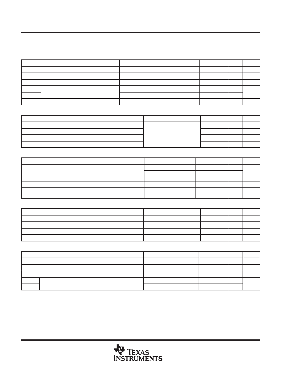
PARAMETER TEST CONDITIONS MIN TYP MAX UNIT
V
ref
R
(EGIN)
R
(EFL)
V
(RTC1)
R
(RTC2)
I
OS
undervoltage lockout section
V
IH
V
IL
V
hys
V
R
Output voltage (pin 16) TA = 25°C, I
Input regulation VOS = 3.1 V to 12 V, I
Output regulation I
p
Short-circuit output current V
PARAMETER TEST CONDITIONS MIN TYP MAX UNIT
Upper threshold voltage 2.7 V
Lower threshold voltage
Hysteresis
Reset threshold voltage (VCC) 2.2 2.3 V
p
= –0.1 mA to –1 mA 1 7.5 mV
(OR)
TA = 20°C to 25°C –0.2% ±2%
TA = 25°C to 75°C –0.2% ±2%
= 0 V 4 8 mA
ref
=
A
= –1 mA 1.485 1.50 1.515 V
(OR)
= –1 mA 2 12.5 mV
(OR)
°
2.5 V
0.1 0.2 V
output voltage monitor section
PARAMETER TEST CONDITIONS MIN TYP MAX UNIT
V
IO(M)
I
(BOM)
V
(IOM)
Input offset voltage
Input bias current VI = 0 V –200 –500 nA
Input voltage range VCC = 3.1 V ~ 12 V
protection control section
PARAMETER TEST CONDITIONS MIN TYP MAX UNIT
V
(tPC)
V
(stby)
V
I
I
(bPC)
Input threshold voltage (pin 15) TA = 25°C 1.45 1.50 1.55 V
Standby voltage (pin 15) 40 70 100 mV
Latched input voltage (pin 15) 10 30 mV
Input source current (pin 15) TA = 25°C –1 –3 –6 µA
oscillator section
PARAMETER TEST CONDITIONS MIN TYP MAX UNIT
f
(OSC)
f
(dev)
f
(dV)
f
(dT1)
f
(dT2)
Frequency Ct = 100 pF, Rt = 10 kΩ 1 MHz
Standard deviation of frequency All values are constant 7%
Frequency change with voltage VCC = 3 V ~ 12 V 1%
TA = 25°C (CH-1,2) 0
VI = 1.5 V (pins 6 and 9),
TA = 25°C (CH-3,4)
VCC–1.8
p
TA = 20°C to 25°C –0.5% ±4%
TA = 25°C to 75°C 0.5% ±4%
10.5
0 to
V
V
6
POST OFFICE BOX 655303 • DALLAS, TEXAS 75265
Page 7

In ut threshold voltage
V
V
Common-mode input voltage
V
V
V
Maximum output voltage swing
V
I
Output current (sink)
mA
TL1464I
QUAD PULSE-WIDTH-MODULATION CONTROL CIRCUIT
SLVS266 – FEBRUAR Y 2000
electrical characteristics over recommended operating free-air temperature range, VCC = 6 V, f =
1 MHz (unless otherwise noted) (continued)
dead-time control section
PARAMETER TEST CONDITIONS MIN TYP MAX UNIT
I
(Idt)
I
(dt)
V
(dt)
V
IO
V
(tt00)
error-amplifier section
V
IO
I
IO
I
IB
ICR
A
(v)
B1 Unity-gain bandwidth 6 MHz
CMRR Common-mode rejection ratio VIC = –0.1 V ~ VCC – 1.8 V 60 80 dB
V
OM+
V
OM–
I
O(vr+)
I
I+
I
OM–
Input current –1 –4 µA
Latched mode sink current TA = 25°C 0.3 1 2 mA
Latched input voltage I
p
PARAMETER TEST CONDITIONS MIN TYP MAX UNIT
Input offset voltage VO = 1 V ±10 mV
Input offset current VO = 1 V ±100 nA
Input bias current VO = 1 V –200 –500 nA
CH-1,2
p
CH-3,4
Open-loop voltage amplification RI = 200 kΩ 60 75 dB
p
Output current (sink) VID = –0.1 V, VO = 1.25 V 0.5 1 mA
Sink current (pin 24) (standby mode)
Output current (source) VID = 0.1 V, VO = 0.75 V –45 –85 µA
= 100 µA 0.5 V
(dt)
Zero duty cycle 0.6 0.7 0.8
100% duty cycle 1.3 1.4 1.5
–0.1 to
= 3.1 V ~ 12
CC
VI = 0.3 V (pin 24)
VI = 0 V (pin 20)
VCC–1.8
0 to
VCC–1.8
V
–0.1
ref
0.1 0.5 mA
0.2
output section
(SINK)
p
total device
I
O(CS)
I
O(CA)
Standby supply current Standby pin input voltage = 0 V 1 200 µA
Average supply current Rt = 10 kΩ 4 7 mA
PARAMETER TEST CONDITIONS MIN TYP MAX UNIT
R
= 2.4 kΩ 15 20 25
(BIAS)
R
= 5.8 kΩ 7.5 10 12.5
(BIAS)
PARAMETER TEST CONDITIONS MIN TYP MAX UNIT
POST OFFICE BOX 655303 • DALLAS, TEXAS 75265
7
Page 8

TL1464I
p
p
QUAD PULSE-WIDTH-MODULATION CONTROL CIRCUIT
SLVS266 – FEBRUAR Y 2000
WAVEFORM (see Note A)
OSCILLATOR
DEAD-TIME
INPUT VOLTAGE
ERROR AMP. OUTPUT
PWM COMP. OUTPUT
OUTPUT PIN WAVEFORM
REGULATED OUTPUT
VOLTAGE (see Note B)
SCP PIN WAVEFORM
SCP COMP. OUTPUT
POWER SUPPLY
VOLTAGE
OSCILLAT OR
WAVEFORM (see Note A)
ERROR AMP. OUTPUT
PWM COMP. OUTPUT
OUTPUT PIN WAVEFORM
REGULATED OUTPUT
VOLTAGE (see Note B)
SCP PIN WAVEFORM
SCP COMP. OUTPUT
POWER SUPPLY
VOLTAGE
2.7 V
2.7 V
V
A
V
A
Protection Enable Time, t
Figure 1. Timing Diagram (CH-1/CH-2)
V
A
V
A
Protection Enable Time, tpe = 477×103 Cpe (sec)
1.4 V
0.7 V
0 V
“H”
(sec)
e
“L”
“H”
“L”
0 V
V
ref
1.5 V
“H”
“L”
V
CC
0 V
1.4 V
0.7 V
“H”
“L”
“H”
“L”
0 V
V
ref
1.5 V
“H”
“L”
V
CC
0 V
+ 0.7 V
+ 0.7 V
DEAD-TIME 100%
V
A
t
pe
= 477×103 C
e
DEAD-TIME 100%
V
A
t
pe
Figure 2. Timing Diagram (CH-3/CH-4)
NOTES: A. Oscillator waveform of CH-1 and CH-2 is inverting output each other.
8
B. Va = input voltage of pin 29 (pin 24)
POST OFFICE BOX 655303 • DALLAS, TEXAS 75265
Page 9

TL1464I
QUAD PULSE-WIDTH-MODULATION CONTROL CIRCUIT
SLVS266 – FEBRUAR Y 2000
MECHANICAL DATA
PT (S-PQFP-G48) PLASTIC QUAD FLATPACK
37
48
0,50
1,45
1,35
36
0,27
0,17
25
24
13
1
5,50 TYP
7,20
SQ
6,80
9,20
SQ
8,80
12
0,08
M
0,05 MIN
0,13 NOM
Gage Plane
0,25
0°–7°
1,60 MAX
NOTES: A. All linear dimensions are in millimeters.
B. This drawing is subject to change without notice.
C. Falls within JEDEC MS-026
D. This may also be a thermally enhanced plastic package with leads conected to the die pads.
Seating Plane
0,10
0,75
0,45
4040052/C 11/96
POST OFFICE BOX 655303 • DALLAS, TEXAS 75265
9
Page 10

PACKAGE OPTION ADDENDUM
www.ti.com
30-Mar-2005
PACKAGING INFORMATION
Orderable Device Status
(1)
Package
Type
Package
Drawing
Pins Package
Qty
Eco Plan
TL1464IPT ACTIVE LQFP PT 48 250 TBD CU NIPDAU Level-2-220C-1 YEAR
TL1464IPTG4 ACTIVE LQFP PT 48 250 Green (RoHS &
no Sb/Br)
TL1464IPTR ACTIVE LQFP PT 48 1000 TBD CU NIPDAU Level-2-220C-1 YEAR
(1)
The marketing status values are defined as follows:
ACTIVE: Product device recommended for new designs.
LIFEBUY: TI has announced that the device will be discontinued, and a lifetime-buy period is in effect.
NRND: Not recommended for new designs. Device is in production to support existing customers, but TI does not recommend using this part in
a new design.
PREVIEW: Device has been announced but is not in production. Samples may or may not be available.
OBSOLETE: TI has discontinued the production of the device.
(2)
Eco Plan - The planned eco-friendly classification: Pb-Free (RoHS) or Green (RoHS & no Sb/Br) - please check
http://www.ti.com/productcontent for the latest availability information and additional product content details.
TBD: The Pb-Free/Green conversion plan has not been defined.
Pb-Free (RoHS): TI's terms "Lead-Free" or "Pb-Free" mean semiconductor products that are compatible with the current RoHS requirements
for all 6 substances, including the requirement that lead not exceed 0.1% by weight in homogeneous materials. Where designed to be soldered
at high temperatures, TI Pb-Free products are suitable for use in specified lead-free processes.
Green (RoHS & no Sb/Br): TI defines "Green" to mean Pb-Free (RoHS compatible), and free of Bromine (Br) and Antimony (Sb) based flame
retardants (Br or Sb do not exceed 0.1% by weight in homogeneous material)
(2)
Lead/Ball Finish MSL Peak Temp
CU NIPDAU Level-3-260C-168 HR
(3)
(3)
MSL, Peak Temp. -- The Moisture Sensitivity Level rating according to the JEDEC industry standard classifications, and peak solder
temperature.
Important Information and Disclaimer:The information provided on this page represents TI's knowledge and belief as of the date that it is
provided. TI bases its knowledge and belief on information provided by third parties, and makes no representation or warranty as to the
accuracy of such information. Efforts are underway to better integrate information from third parties. TI has taken and continues to take
reasonable steps to provide representative and accurate information but may not have conducted destructive testing or chemical analysis on
incoming materials and chemicals. TI and TI suppliers consider certain information to be proprietary, and thus CAS numbers and other limited
information may not be available for release.
In no event shall TI's liability arising out of such information exceed the total purchase price of the TI part(s) at issue in this document sold by TI
to Customer on an annual basis.
Addendum-Page 1
Page 11

IMPORTANT NOTICE
Texas Instruments Incorporated and its subsidiaries (TI) reserve the right to make corrections, modifications,
enhancements, improvements, and other changes to its products and services at any time and to discontinue
any product or service without notice. Customers should obtain the latest relevant information before placing
orders and should verify that such information is current and complete. All products are sold subject to TI’s terms
and conditions of sale supplied at the time of order acknowledgment.
TI warrants performance of its hardware products to the specifications applicable at the time of sale in
accordance with TI’s standard warranty. Testing and other quality control techniques are used to the extent TI
deems necessary to support this warranty . Except where mandated by government requirements, testing of all
parameters of each product is not necessarily performed.
TI assumes no liability for applications assistance or customer product design. Customers are responsible for
their products and applications using TI components. To minimize the risks associated with customer products
and applications, customers should provide adequate design and operating safeguards.
TI does not warrant or represent that any license, either express or implied, is granted under any TI patent right,
copyright, mask work right, or other TI intellectual property right relating to any combination, machine, or process
in which TI products or services are used. Information published by TI regarding third-party products or services
does not constitute a license from TI to use such products or services or a warranty or endorsement thereof.
Use of such information may require a license from a third party under the patents or other intellectual property
of the third party, or a license from TI under the patents or other intellectual property of TI.
Reproduction of information in TI data books or data sheets is permissible only if reproduction is without
alteration and is accompanied by all associated warranties, conditions, limitations, and notices. Reproduction
of this information with alteration is an unfair and deceptive business practice. TI is not responsible or liable for
such altered documentation.
Resale of TI products or services with statements different from or beyond the parameters stated by TI for that
product or service voids all express and any implied warranties for the associated TI product or service and
is an unfair and deceptive business practice. TI is not responsible or liable for any such statements.
Following are URLs where you can obtain information on other Texas Instruments products and application
solutions:
Products Applications
Amplifiers amplifier.ti.com Audio www.ti.com/audio
Data Converters dataconverter.ti.com Automotive www.ti.com/automotive
DSP dsp.ti.com Broadband www.ti.com/broadband
Interface interface.ti.com Digital Control www.ti.com/digitalcontrol
Logic logic.ti.com Military www.ti.com/military
Power Mgmt power.ti.com Optical Networking www.ti.com/opticalnetwork
Microcontrollers microcontroller.ti.com Security www.ti.com/security
Telephony www.ti.com/telephony
Video & Imaging www.ti.com/video
Wireless www.ti.com/wireless
Mailing Address: Texas Instruments
Post Office Box 655303 Dallas, Texas 75265
Copyright 2005, Texas Instruments Incorporated
 Loading...