Page 1
查询TL1451A供应商
TL1451A
DUAL PULSE-WIDTH-MODULATION CONTROL CIRCUITS
SLVS024E – FEBRUARY 1983 – REVISED NOVEMBER 1999
D
Complete PWM Power Control Circuitry
D
Completely Synchronized Operation
D
Internal Undervoltage Lockout Protection
D
Wide Supply Voltage Range
D
Internal Short-Circuit Protection
D
Oscillator Frequency . . . 500 kHz Max
D
Variable Dead Time Provides Control Over
Total Range
D
Internal Regulator Provides a Stable 2.5-V
Reference Supply
D
Available in Q-Temp Automotive
HighRel Automotive Applications
Configuration Control / Print Support
Qualification to Automotive Standards
description
The TL1451A incorporates on a single monolithic
chip all the functions required in the construction
of two pulse-width-modulation (PWM) control
circuits. Designed primarily for power-supply
control, the TL1451A contains an on-chip 2.5-V
regulator, two error amplifiers, an adjustable
oscillator, two dead-time comparators, undervoltage lockout circuitry, and dual common-emitter
output transistor circuits.
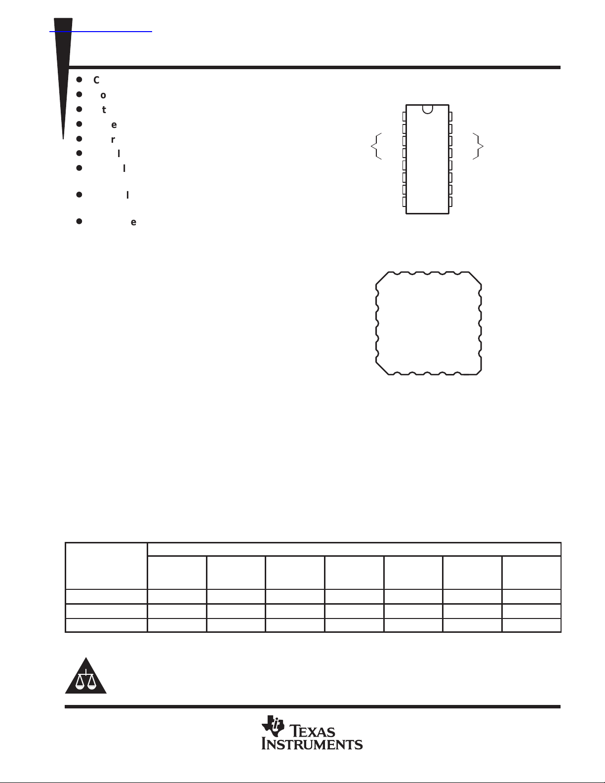
ERROR 1IN+
AMPLIFIER 1 1IN–
1FEEDBACK
D, DB, N, NS, PW, OR J PACKAGE
1FEEDBACK
1DTC
1OUT
1IN+
1IN–
NC
IDTC
CT
RT
GND
RTCTNC
4
5
6
7
8
1OUT
(TOP VIEW)
16
1
15
2
14
3
13
4
12
5
11
6
10
7
8
FK PACKAGE
(TOP VIEW)
9
REF
NC
GND
V
REF
SCP
2IN+ ERROR
2IN– AMPLIFIER 2
2FEEDBACK
2DTC
2OUT
V
CC
SCP
1920132
2IN+
18
2IN–
17
NC
16
2FEEDBACK
15
2DTC
14
1312119 10
CC
OUT
The uncommitted output transistors provide
common-emitter output capability for each
controller. The internal amplifiers exhibit a common-mode voltage range from 1.04 V to 1.45 V. The dead-time
control (DTC) comparator has no offset unless externally altered and can provide 0% to 100% dead time. The
on-chip oscillator can be operated by terminating RT and CT. During low V
conditions, the undervoltage
CC
lockout control circuit feature locks the outputs off until the internal circuitry is operational.
The TL1451AC is characterized for operation from –20°C to 85°C. The TL1451AQ is characterized for operation
from –40°C to 125°C. The TL1451AM is characterized for operation from –55°C to 125°C.
AVAILABLE OPTIONS
PACKAGED DEVICES
T
A
–20°C to 85°C — TL1451ACDB TL1451ACN TL1451ACNS TL1451ACPW — —
–40°C to 125°C TL1451AQD — — — — — —
–55°C to 125°C — — — — — TL1451AMFK TL1451AMJ
†
The DB and PW packages are only available left-end taped and reeled (add LE suffix, i.e., TL1451ACPWLE).
Please be aware that an important notice concerning availability, standard warranty, and use in critical applications of
Texas Instruments semiconductor products and disclaimers thereto appears at the end of this data sheet.
PRODUCTION DATA information is current as of publication date.
Products conform to specifications per the terms of Texas Instruments
standard warranty. Production processing does not necessarily include
testing of all parameters.
SMALL
OUTLINE
(D)
SMALL
OUTLINE
(DB)
POST OFFICE BOX 655303 • DALLAS, TEXAS 75265
†
PLASTIC DIP
(N)
SMALL
OUTLINE
(NS)
TSSOP
†
(PW)
Copyright 1999, Texas Instruments Incorporated
On products compliant to MIL-PRF-38535, all parameters are tested
unless otherwise noted. On all other products, production
processing does not necessarily include testing of all parameters.
CHIP
CARRIER
(FK)
CERAMIC
DIP
(J)
1
Page 2
TL1451A
DUAL PULSE-WIDTH-MODULATION CONTROL CIRCUITS
SLVS024E – FEBRUARY 1983 – REVISED NOVEMBER 1999
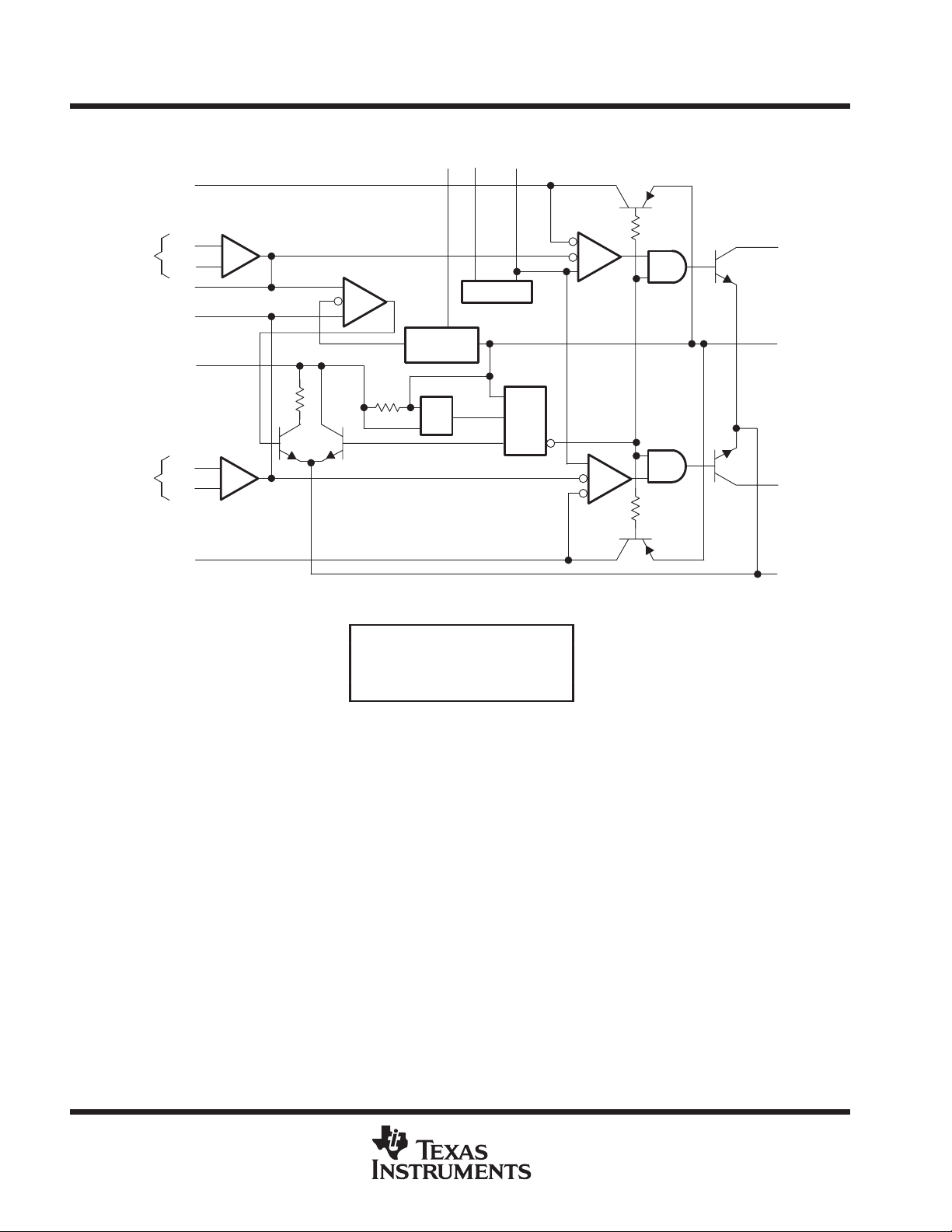
functional block diagram
VCCRT CT
2 DTC
11
92 1
ERROR
AMPLIFIER 2
2 FEEDBACK
1 FEEDBACK
ERROR
AMPLIFIER 1
IN+
IN–
SCP
IN+
IN–
1 DTC
14
13
12
5
15
3
4
6
+
–
PWM
COMP
PWM
COMP
R
S
Oscillator
R
1/2 V
ref
Reference
12 kΩ
170 kΩ UVLO
+
–
Resistors 65
Capacitors 8
Transistors 105
JFETs 18
Voltage
COMPONENT COUNT
10
2 OUTPUT
16
REF
7
1 OUTPUT
8
GND
2
POST OFFICE BOX 655303 • DALLAS, TEXAS 75265
Page 3
TL1451A
DUAL PULSE-WIDTH-MODULATION CONTROL CIRCUITS
SLVS024E – FEBRUARY 1983 – REVISED NOVEMBER 1999
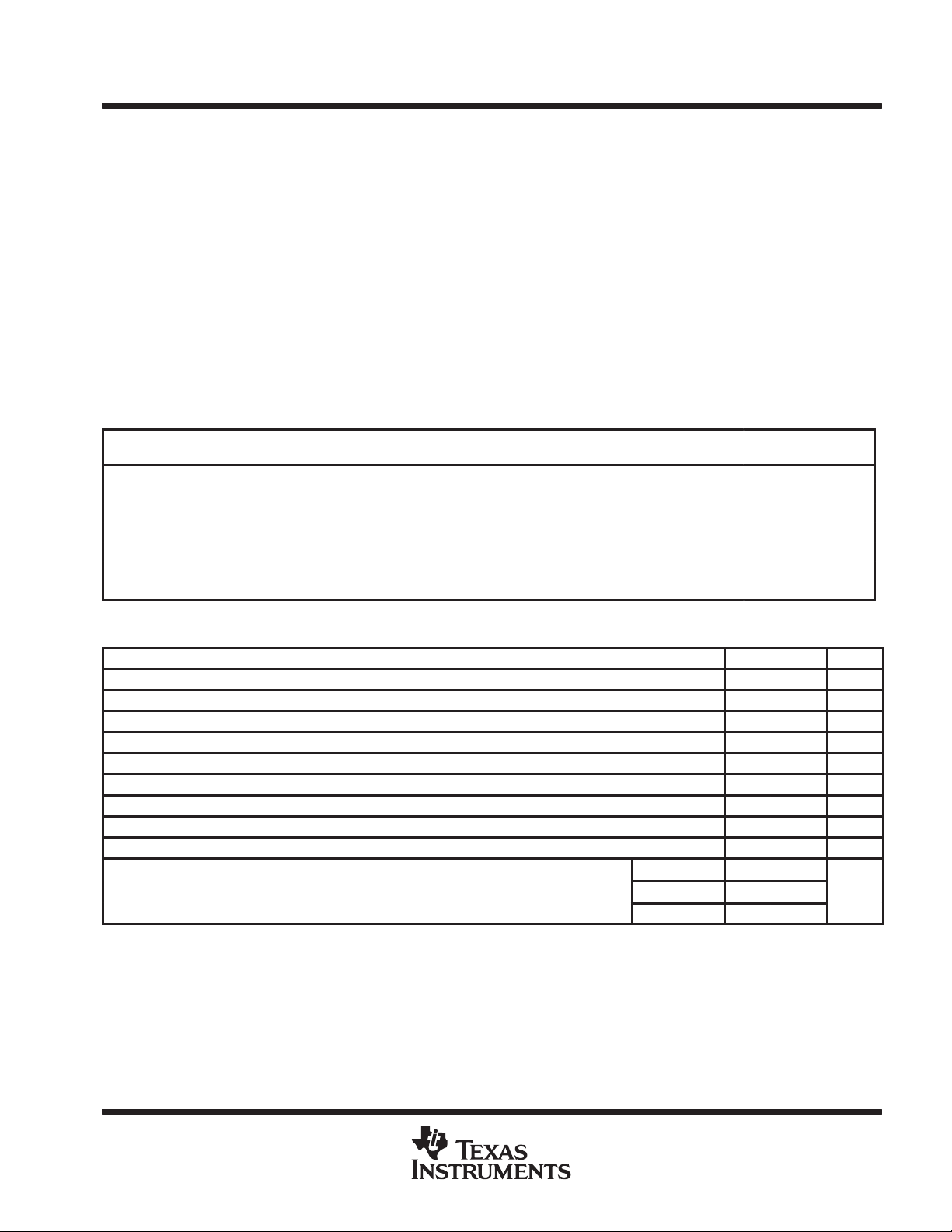
absolute maximum ratings over operating free-air temperature range
†
Supply voltage, VCC 51 V. . . . . . . . . . . . . . . . . . . . . . . . . . . . . . . . . . . . . . . . . . . . . . . . . . . . . . . . . . . . . . . . . . . . . . .
Amplifier input voltage, VI 20 V. . . . . . . . . . . . . . . . . . . . . . . . . . . . . . . . . . . . . . . . . . . . . . . . . . . . . . . . . . . . . . . . . . .
Collector output voltage, VO 51 V. . . . . . . . . . . . . . . . . . . . . . . . . . . . . . . . . . . . . . . . . . . . . . . . . . . . . . . . . . . . . . . . .
Collector output current, I
21 mA. . . . . . . . . . . . . . . . . . . . . . . . . . . . . . . . . . . . . . . . . . . . . . . . . . . . . . . . . . . . . . . .
O
Continuous power total dissipation See Dissipation Rating Table. . . . . . . . . . . . . . . . . . . . . . . . . . . . . . . . . . . . .
Operating free-air temperature range, TA C suffix –20°C to 85°C. . . . . . . . . . . . . . . . . . . . . . . . . . . . . . . . . . . . .
Q suffix –40°C to 125°C. . . . . . . . . . . . . . . . . . . . . . . . . . . . . . . . . . . .
M suffix –55°C to 125°C. . . . . . . . . . . . . . . . . . . . . . . . . . . . . . . . . . . .
Storage temperature range, T
–65°C to 150°C. . . . . . . . . . . . . . . . . . . . . . . . . . . . . . . . . . . . . . . . . . . . . . . . . . .
stg
Lead temperature 1,6 mm (1/16 inch) from case for 10 seconds 260°C. . . . . . . . . . . . . . . . . . . . . . . . . . . . . . .
†
Stresses beyond those listed under “absolute maximum ratings” may cause permanent damage to the device. These are stress ratings only, and
functional operation of the device at these or any other conditions beyond those indicated under “recommended operating conditions” is not
implied. Exposure to absolute-maximum-rated conditions for extended periods may affect device reliability.
DISSIPATION RATING TABLE
PACKAGE
D 1088 mW 8.7 mW/°C 696 mW 566 mW 218 mW
DB 775 mW 6.2 mW/°C 496 mW 403 mW —
N 1000 mW 8.0 mW/°C 640 mW 520 mW —
NS 500 mW 4.0 mW/°C 320 mW 260 mW —
PW 838 mW 6.7 mW/°C 536 mW 436 mW 168 mW
FK 1375 mW 11.0 mW/°C 880 mW 715 mW 275 mW
J 1375 mW 1 1.0 mW/°C 880 mW 715 mW 275 mW
TA ≤ 25°C
POWER RATING
DERATING FACTOR
ABOVE TA = 25°C
TA = 70°C
POWER RATING
TA = 85°C
POWER RATING
TA = 125°C
POWER RATING
recommended operating conditions
MIN MAX UNIT
Supply voltage, V
Amplifier input voltage, V
Collector output voltage, V
Collector output current, I
Current into feedback terminal 45 µA
Feedback resistor, R
Timing capacitor , C
Timing resistor , R
Oscillator frequency 1 500 kHz
Operating free-air temperature, T
CC
T
I
O
O
F
T
C suffix –20 85
A
Q suffix –40 125
M suffix –55 125
3.6 50 V
1.05 1.45 V
50 V
20 mA
100 kΩ
150 15000 pF
5.1 100 kΩ
°C
POST OFFICE BOX 655303 • DALLAS, TEXAS 75265
3
Page 4
TL1451A
PARAMETER
TEST CONDITIONS
UNIT
Output voltage change with temperature
PARAMETER
TEST CONDITIONS
UNIT
I
T
25°C
PARAMETER
TEST CONDITIONS
UNIT
PARAMETER
TEST CONDITIONS
UNIT
Frequency change with temperature
DUAL PULSE-WIDTH-MODULATION CONTROL CIRCUITS
SLVS024E – FEBRUARY 1983 – REVISED NOVEMBER 1999
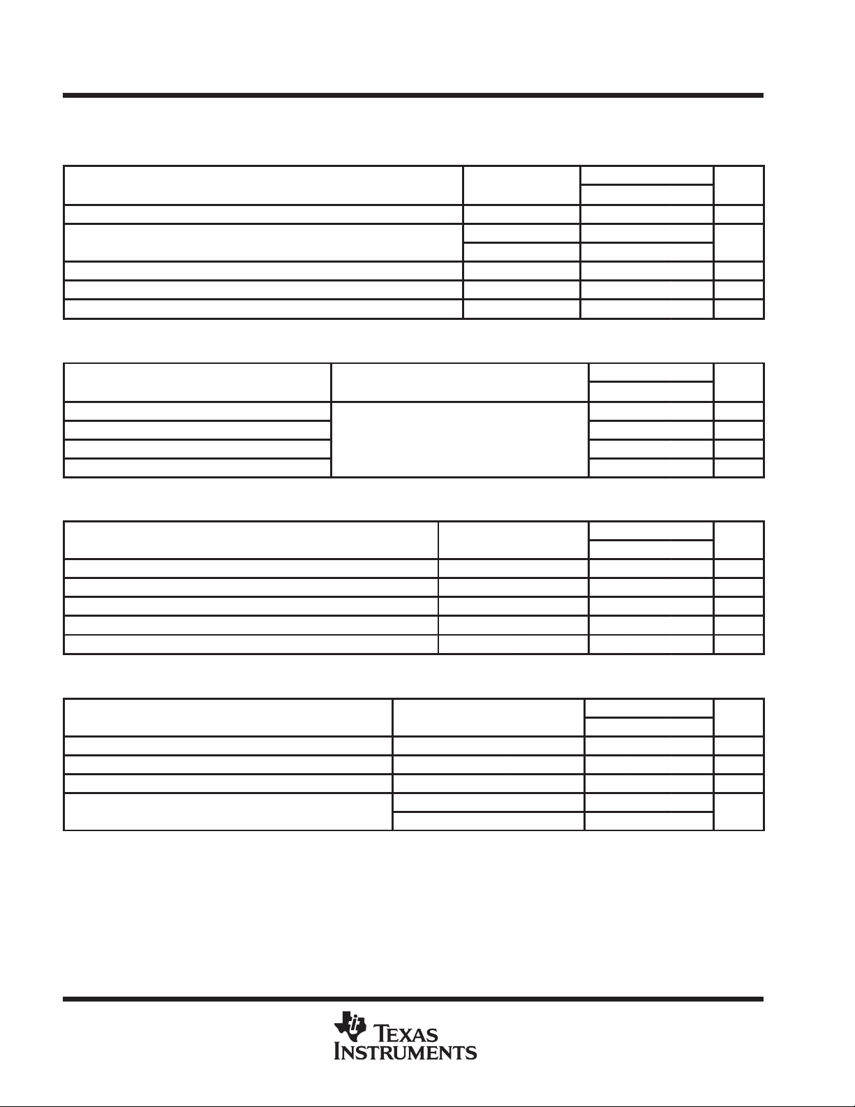
electrical characteristics over recommended operating free-air temperature range, VCC = 6 V,
f = 200 kHz (unless otherwise noted)
reference section
TL1451AC
MIN
Output voltage (pin 16) IO = 1 mA 2.4 2.5 2.6 V
p
Input voltage regulation VCC = 3.6 V to 40 V 2 12.5 mV
Output voltage regulation IO = 0.1 mA to 1 mA 1 7.5 mV
Short-circuit output current VO = 0 3 10 30 mA
†
All typical values are at TA = 25°C.
p
TA = –20°C to 25°C –0.1% ±1%
TA = 25°C to 85°C –0.2% ±1%
undervoltage lockout section
MIN
Upper threshold voltage (VCC) 2.72 V
Lower threshold voltage (VCC)
Hysteresis (VCC)
Reset threshold voltage (VCC) 1.5 1.9 V
†
All typical values are at TA = 25°C.
O(ref)
= 0.1 mA,
°
=
A
80 120 mV
†
TYP
TL1451AC
†
TYP
2.6 V
MAX
MAX
short-circuit protection control section
TL1451AC
MIN TYP†MAX
Input threshold voltage (SCP) TA = 25°C 0.65 0.7 0.75 V
Standby voltage (SCP) No pullup 140 185 230 mV
Latched input voltage (SCP) No pullup 60 120 mV
Input (source) current VI = 0.7 V, TA = 25°C –10 –15 –20 µA
Comparator threshold voltage (FEEDBACK) 1.18 V
†
All typical values are at TA = 25°C.
oscillator section
TL1451C
MIN TYP†MAX
Frequency CT = 330 pF, RT = 10 kΩ 200 kHz
Standard deviation of frequency CT = 330 pF, RT = 10 kΩ 10%
Frequency change with voltage VCC = 3.6 V to 40 V 1%
p
†
All typical values are at TA = 25°C.
TA = –20°C to 25°C –0.4% ±2%
TA = 25°C to 85°C –0.2% ±2%
4
POST OFFICE BOX 655303 • DALLAS, TEXAS 75265
Page 5
TL1451A
PARAMETER
TEST CONDITIONS
UNIT
Input threshold voltage at f
(DTC)
V
PARAMETER
TEST CONDITIONS
UNIT
1.05
gg
CC
PARAMETER
TEST CONDITIONS
UNIT
PARAMETER
TEST CONDITIONS
UNIT
Input threshold voltage at f
(FEEDBACK)
V
PARAMETER
TEST CONDITIONS
UNIT
DUAL PULSE-WIDTH-MODULATION CONTROL CIRCUITS
SLVS024E – FEBRUARY 1983 – REVISED NOVEMBER 1999
dead-time control section
TL1451AC
MIN TYP†MAX
Input bias current (DTC) 1 µA
Latch mode (source) current (DTC) TA = 25°C –80 –145 µA
Latched input voltage (DTC) IO = 40 µA 2.3 V
p
†
All typical values are at TA = 25°C.
= 10 kHz
error-amplifier section
Input offset voltage VO (FEEDBACK) = 1.25 V ±6 mV
Input offset current VO (FEEDBACK) = 1.25 V ±100 nA
Input bias current VO (FEEDBACK) = 1.25 V 160 500 nA
Common-mode input voltage range VCC = 3.6 V to 40 V
Open-loop voltage amplification RF = 200 kΩ 70 80 dB
Unity-gain bandwidth 1.5 MHz
Common-mode rejection ratio 60 80 dB
Positive output voltage swing V
Negative output voltage swing 1 V
Output (sink) current (FEEDBACK) VID = –0.1 V, VO = 1.25 V 0.5 1.6 mA
Output (source) current (FEEDBACK) VID = 0.1 V, VO = 1.25 V –45 –70 µA
†
All typical values are at TA = 25°C.
Zero duty cycle 2.05 2.25
Maximum duty cycle 1.2 1.45
TL1451AC
MIN TYP†MAX
1.05
to
1.45
–0.1 V
ref
V
output section
TL1451AC
MIN TYP†MAX
Collector off-state current VO = 50 V 10 µA
Output saturation voltage IO = 10 mA 1.2 2 V
Short-circuit output current VO = 6 V 90 mA
†
All typical values are at TA = 25°C.
pwm comparator section
TL1451AC
MIN TYP†MAX
p
†
All typical values are at TA = 25°C.
= 10 kHz
Zero duty cycle 2.05 2.25
Maximum duty cycle 1.2 1.45
total device
TL1451AC
MIN TYP†MAX
Standby supply current Off-state 1.3 1.8 mA
Average supply current RT = 10 kΩ 1.7 2.4 mA
†
All typical values are at TA = 25°C.
POST OFFICE BOX 655303 • DALLAS, TEXAS 75265
5
Page 6
TL1451A
PARAMETER
TEST CONDITIONS
UNIT
Output voltage (pin 16)
I
mA
V
PARAMETER
TEST CONDITIONS
UNIT
DUAL PULSE-WIDTH-MODULATION CONTROL CIRCUITS
SLVS024E – FEBRUARY 1983 – REVISED NOVEMBER 1999
electrical characteristics over recommended operating free-air temperature range, VCC = 6 V,
f = 200 kHz (unless otherwise noted)
reference section
TL1451AQ, TL1451AM
MIN
p
Output voltage change with temperature –0.63% *±4%
Input voltage regulation VCC = 3.6 V to 40 V
Output voltage regulation IO = 0.1 mA to 1 mA
Short-circuit output current VO = 0 3 10 30 mA
*These parameters are not production tested.
†
All typical values are at TA = 25°C unless otherwise indicated.
p
O
= 1
TA = 25°C 2.40 2.50 2.60
TA = MIN and 125°C 2.35 2.46 2.65
TA = 25°C 2.0 12.5
TA = 125°C 0.7 15
TA = MIN 0.3 30
TA = 25°C 1.0 7.5
TA = 125°C 0.3 14
TA = MIN 0.3 20
TYP
†
MAX
mV
mV
undervoltage lockout section
Upper threshold voltage (VCC)
Lower threshold voltage (VCC)
Hysteresis (VCC)
Reset threshold voltage (VCC)
†
All typical values are at TA = 25°C unless otherwise indicated.
TL1451AQ, TL1451AM
MIN
TYP
TA = 25°C 2.72
TA = 125°C 1.70
TA = MIN 3.15
TA = 25°C 2.60
TA = 125°C 1.65
TA = MIN 3.09
TA = 25°C 80 120
TA = 125°C 10 50
TA = MIN 10 60
TA = 25°C 1.50
TA = 125°C 0.95
TA = MIN 1.50
†
MAX
V
V
mV
V
6
POST OFFICE BOX 655303 • DALLAS, TEXAS 75265
Page 7
TL1451A
PARAMETER
TEST CONDITIONS
UNIT
PARAMETER
TEST CONDITIONS
UNIT
R
T
kΩ
PARAMETER
TEST CONDITIONS
UNIT
Input bias current (DTC)
A
Input threshold voltage at f
(DTC)
V
DUAL PULSE-WIDTH-MODULATION CONTROL CIRCUITS
SLVS024E – FEBRUARY 1983 – REVISED NOVEMBER 1999
short-circuit protection control section
TL1451AQ, TL1451AM
MIN TYP†MAX
TA = 25°C 650 700 750
Input threshold voltage (SCP)
Standby voltage (SCP) 140 185 230 mV
Latched input voltage (SCP)
Equivalent timing resistance 170 kΩ
Comparator threshold voltage (FEEDBACK) 1.18 V
†
All typical values are at TA = 25°C unless otherwise indicated.
oscillator section
Frequency
Standard deviation of frequency CT = 330 pF, RT = 10 kΩ 2%
Frequency change with voltage VCC = 3.6 V to 40 V
Frequency change with temperature 1.37% *±10%
*These parameters are not production tested.
†
All typical values are at TA = 25°C unless otherwise indicated.
CT = 330 pF,
TA = 125°C 400 478 550
TA = MIN 800 880 950
TA = 25°C 60 120
TA = 125°C 70 120
TA = MIN 60 120
TL1451AQ, TL1451AM
MIN TYP†MAX
TA = 25°C 200
= 10
TA = 125°C 195
TA = MIN 193
TA = 25°C 1%
TA = 125°C 1%
TA = MIN 3%
mV
mV
kHz
dead-time control section
TL1451AQ, TL1451AM
MIN TYP†MAX
p
Latch mode (source) current (DTC) –80 –145 µA
Latched input voltage (DTC)
p
*These parameters are not production tested.
†
All typical values are at TA = 25°C unless otherwise indicated.
= 10 kHz
TA = 25°C 1
TA = MIN and 125°C 3
TA = 25°C 2.30
TA = 125°C 2.22 2.32
TA = MIN 2.28 2.40
Zero duty cycle 2.05 *2.25
Maximum duty cycle *1.20 1.45
µ
V
POST OFFICE BOX 655303 • DALLAS, TEXAS 75265
7
Page 8
TL1451A
PARAMETER
TEST CONDITIONS
UNIT
1.05
gg
CC
PARAMETER
TEST CONDITIONS
UNIT
PARAMETER
TEST CONDITIONS
UNIT
Input threshold voltage at f
(FEEDBACK)
V
DUAL PULSE-WIDTH-MODULATION CONTROL CIRCUITS
SLVS024E – FEBRUARY 1983 – REVISED NOVEMBER 1999
error-amplifier section
TL1451AQ, TL1451AM
MIN TYP†MAX
TA = 25°C ±6
Input offset voltage VO (FEEDBACK) = 1.25 V
Input offset current VO (FEEDBACK) = 1.25 V
Input bias current VO (FEEDBACK) = 1.25 V
Common-mode input voltage range VCC = 3.6 V to 40 V
Open-loop voltage amplification RF = 200 kΩ
Unity-gain bandwidth 1.5 MHz
Common-mode rejection ratio 60 80 dB
Positive output voltage swing 2 V
Negative output voltage swing 1 V
Output (sink) current (FEEDBACK) VID = –0.1 V, VO = 1.25 V
Output (source) current (FEEDBACK) VID = 0.1 V, VO = 1.25 V
†
All typical values are at TA = 25°C unless otherwise indicated.
TA = 125°C ±10
TA = MIN ±12
TA = 25°C ±100
TA = 125°C ±100
TA = MIN ±200
TA = 25°C 160 500
TA = 125°C 100 500
TA = MIN 142 700
1.05
to
1.45
TA = 25°C 70 80
TA = 125°C 70 80
TA = MIN 64 80
TA = 25°C 0.5 1.6
TA = 125°C 0.4 1.8
TA = MIN 0.3 1.7
TA = 25°C –45 –70
TA = 125°C –25 –50
TA = MIN –15 –70
mV
nA
nA
V
dB
mA
µA
output section
TL1451AQ, TL1451AM
MIN TYP†MAX
Collector off-state current VO = 50 V 10 µA
TA = 25°C 1.20 2.0
Output saturation voltage
Short-circuit output current VO = 6 V 90 mA
†
All typical values are at TA = 25°C unless otherwise indicated.
TA = 125°C 1.60 2.4
TA = MIN
1.36 2.2
pwm comparator section
TL1451AQ, TL1451AM
MIN TYP†MAX
p
*These parameters are not production tested.
†
All typical values are at TA = 25°C unless otherwise indicated.
= 10 kHz
Zero duty cycle 2.05 *2.25
Maximum duty cycle *1.20 1.45
V
8
POST OFFICE BOX 655303 • DALLAS, TEXAS 75265
Page 9
TL1451A
PARAMETER
TEST CONDITIONS
UNIT
DUAL PULSE-WIDTH-MODULATION CONTROL CIRCUITS
SLVS024E – FEBRUARY 1983 – REVISED NOVEMBER 1999
total device
TL1451AQ, TL1451AM
MIN TYP†MAX
Standby supply current Off-state 1.3 1.8 mA
Average supply current RT = 10 kΩ 1.7 2.4 mA
†
All typical values are at TA = 25°C unless otherwise indicated.
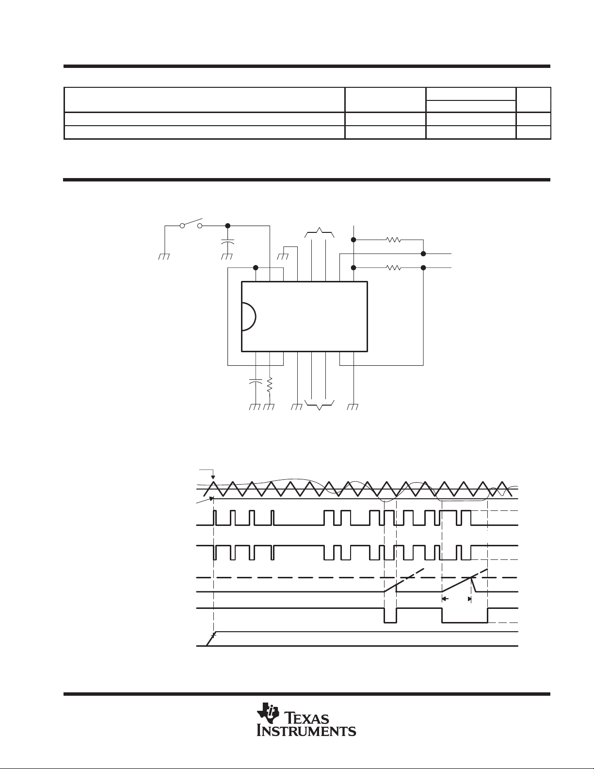
PARAMETER MEASUREMENT INFORMATION
S1
C
PE
C
330 pF
0.47 µF
T
Figure 1. Test Circuit
Oscillator Triangle Waveform
Error Amplifier Output
Dead-Time Input Voltage
Short-Circuit Protection
Comparator Input Voltage
PWM Comparator Output Voltage
Output Transistor Collector
Protection Enable
Terminal Waveform
Short-Circuit Protection
Comparator Output
Power Supply Voltage
†
Protection Enable Time, tpe = (0.051 x 10⁶ x Cpe) in seconds
Waveform
2.8 V TYP
TL1451A
R
T
10 kΩ
Test
Input
Test
Input
VCC = 5 V
910111213141516
87654321
R
L
4.7 kΩ
R
L
4.7 kΩ
OUT1
OUT2
Dead Time 100%
†
t
pe
2.0 V
1.6 V
1.4 V
1.25 V
H
L
H
L
0.6 V
0 V
H
L
3.6 V
0 V
Figure 2. TL1451A Timing Diagram
POST OFFICE BOX 655303 • DALLAS, TEXAS 75265
9
Page 10

TL1451A
DUAL PULSE-WIDTH-MODULATION CONTROL CIRCUITS
SLVS024E – FEBRUARY 1983 – REVISED NOVEMBER 1999
TYPICAL CHARACTERISTICS
TRIANGLE OSCILLATOR FREQUENCY
vs
TIMING RESISTANCE
1 M
VCC = 5 V
TA = 25°C
CT = 150 pF
100 k
CT = 1500 pF
10 k
osc
fosc – Triangle Oscillator Frequency – Hz
f
1 k
1 k 4 k 10 k 40 k 100 k 400 k 1 M
RT – Timing Resistance – Ω
CT = 15000 pF
Figure 3 Figure 4
OSCILLATOR FREQUENCY VARIATION
FREE-AIR TEMPERATURE
3
VCC = 3.6 V
RT = 10 kΩ
CT = 330 pF
2
f
= 200 kHz
osc
1
0
–1
–2
osc
f
afosc – Oscillator Frequency Variation – %
∆
–3
–25 0 25 50
TA – Free-Air Temperature – °C
vs
75 100
2.6
2.4
2.2
2
1.8
1.6
1.4
1.2
Triangle W aveform Swing Voltage – V
1
0.8
10
TRIANGLE WAVEFORM SWING VOLTAGE
vs
TIMING CAPACITANCE
VCC = 5 V
RT = 5.1 kΩ
TA = 25°C
1
2
10
CT – Timing Capacitance – pF
10
3
10
4
Figure 5 Figure 6
10
TRIANGLE WAVEFORM PERIOD
vs
TIMING CAPACITANCE
2
10
VCC = 5 V
RT = 5.1 kΩ
10
10
10
1
0
–1
10
TA = 25°C
1
2
10
CT – Timing Capacitance – pF
10
3
10
4
10
5
sµ
Triangle W aveform Period – uS
5
10
POST OFFICE BOX 655303 • DALLAS, TEXAS 75265
Page 11

TL1451A
ОООООО
ОООООО
ОООООО
ОООООО
DUAL PULSE-WIDTH-MODULATION CONTROL CIRCUITS
SLVS024E – FEBRUARY 1983 – REVISED NOVEMBER 1999
TYPICAL CHARACTERISTICS
REFERENCE OUTPUT VOLTAGE VARIATION
vs
FREE-AIR TEMPERATURE
30
VCC = 3.6 V
I
= 1 mA
I(ref)
20
10
0
–10
– 20
avref – Reference Output Voltage Variation – mV
O(ref)
V
∆
– 30
– 25 0 25 50
TA – Free-Air Temperature – °C
Figure 7 Figure 8
75 100
REFERENCE OUTPUT VOLTAGE VARIATION
vs
FREE-AIR TEMPERATURE
30
VCC = 40 V
I
= 1 mA
I(ref)
20
10
0
–10
– 20
avref – Reference Output Voltage Variation – mV
O(ref)
V
– 30
∆
– 25 0 25 50
TA – Free-Air Temperature – °C
75 100
REFERENCE OUTPUT VOLTAGE
SUPPLY VOLTAGE
3
TA = 25°C
2.5
2
1.5
1
Vref – Reference Output Voltage – V
O(ref)
0.5
V
0
0 5 10 15 20 25
VCC – Supply Voltage – V
Figure 9 Figure 10
vs
30 35 40
DROPOUT VOLTAGE VARIATION
FREE-TEMPERATURE
1.1
I
= 1 mA
I(ref)
1
0.9
0.8
0.7
Dropout Voltage Variation – V
0.6
– 25 0 25 50
TA – Free-Air Temperature – °C
vs
75 100
POST OFFICE BOX 655303 • DALLAS, TEXAS 75265
11
Page 12

TL1451A
DUAL PULSE-WIDTH-MODULATION CONTROL CIRCUITS
SLVS024E – FEBRUARY 1983 – REVISED NOVEMBER 1999
TYPICAL CHARACTERISTICS
UNDERVOLTAGE LOCKOUT
HYSTERESIS CHARACTERISTICS
6
TA = 85°C
5
4
3
2
CE
1
VCE – Output Collector Voltage – V
V
0
5 V
R
L
7,10
IO = 10 mA
0123
I = I
8
O
V
DE
VCC – Supply Voltage – V
TA = 25°C
TA = –20°C
45
UNDERVOLTAGE LOCKOUT CHARACTERISTIC
3.5
3.25
3
2.75
2.5
Hysteresis Voltage
(Right Scale)
2.25
2
Undervoltage Lockout Threshold Voltage – V
–25 0 25 50
Threshold V oltage –V
(Left Scale)
Threshold Voltage –V
(Left Scale)
TA – Free-Air Temperature – °C
TH
75 100
300
250
200
TL
150
100
50
0
Undervoltage Lockout Hystersis Voltage – mV
Figure 11 Figure 12
SHORT-CIRCUIT PROTECTION CHARACTERISTICS
1.30
1.25
1.20
1.15
Comparator Threshold Voltage – V
1.10
Short-Circuit Protection
Comparator Threshold Voltage
(Left Scale)
– 25 0 25
Short-Circuit Protection
Latch Reset Supply Voltage
(Right Scale)
50 75 100
TA – Free-Air Temperature – °C
3
2.5
2
1.5
RS – Latch Reset Supply Voltage – V
1
Figure 13
12
POST OFFICE BOX 655303 • DALLAS, TEXAS 75265
Page 13

18
15
12
pe
t
tpe – Protection Enable Time – s
TL1451A
DUAL PULSE-WIDTH-MODULATION CONTROL CIRCUITS
SLVS024E – FEBRUARY 1983 – REVISED NOVEMBER 1999
TYPICAL CHARACTERISTICS
PROTECTION ENABLE TIME
vs
PROTECTION ENABLE CAPACITANCE
9
6
3
ERROR AMP 1
ERROR AMP 2
1.25 V
0
Short-circuit
Protection
Comparator
+
–
0 50 100 150
CPE – Protection Enable Capacitance – µF
SCP V
15
12 kΩ
ref
16
C
PE
Figure 14
200 250
170 kΩ
SR
Protection
Latch
V
ref
V
ref
U.V.L.O.
POST OFFICE BOX 655303 • DALLAS, TEXAS 75265
13
Page 14

TL1451A
DUAL PULSE-WIDTH-MODULATION CONTROL CIRCUITS
SLVS024E – FEBRUARY 1983 – REVISED NOVEMBER 1999
TYPICAL CHARACTERISTICS
ERROR AMP MAXIMUM OUTPUT VOLTAGE SWING
vs
FREQUENCY
2.25
VCC = 5 V
2
TA = 25°C
1.75
1.5
1.25
1
0.75
0.5
0.25
Error Amp Maximum Output Voltage Swing – V
0
1 k 10 k 100 k 1 M 10 M
f – Frequency – Hz
Figure 15 Figure 16
OPEN-LOOP VOLTAGE AMPLIFICATION
vs
FREQUENCY
90
80
70
60
50
40
30
20
Open-Loop Voltage Amplification – dB
10
0
100 1 k 10 k 100 k 1 M 2 M
f – Frequency – Hz
VCC = 5 V
TA = 25°C
UNITY-GAIN CONFIGURATION)
10
VCC = 5 V
TA = 25°C
5
0
–5
G – Gain – dB
–10
–15
–20
1 k 10 k 100 k
GAIN (AMPLIFIER IN
vs
FREQUENCY
1 M 10 M
f – Frequency – Hz
Figure 17
14
POST OFFICE BOX 655303 • DALLAS, TEXAS 75265
Page 15

DUAL PULSE-WIDTH-MODULATION CONTROL CIRCUITS
SLVS024E – FEBRUARY 1983 – REVISED NOVEMBER 1999
TYPICAL CHARACTERISTICS
CLOSED-LOOP GAIN AND PHASE SHIFT
vs
FREQUENCY
70
VCC = 5 V
R
= 150 Ω
ref
60
C
= 470 pF
ref
TA = 25°C
50
Closed-Loop Gain
40
30
Closed-Loop Gain – dB
20
10
0
100 1 k 10 k 100 k 1 M
(Left Scale)
f – Frequency – Hz
CX:
Phase Shift
(Right Scale)
47 pF
470 pF
4700 pF
TL1451A
0°
–10°
–20°
–30°
Phase Shift
–40°
–50°
–60°
–70°
–80°
–90°
39 kΩ
39 kΩ
V
ref
C
x
Test Circuit
Figure 18
+
–
R
ref
C
ref
POST OFFICE BOX 655303 • DALLAS, TEXAS 75265
15
Page 16

TL1451A
DUAL PULSE-WIDTH-MODULATION CONTROL CIRCUITS
SLVS024E – FEBRUARY 1983 – REVISED NOVEMBER 1999
TYPICAL CHARACTERISTICS
CLOSED-LOOP GAIN AND PHASE SHIFT
vs
FREQUENCY
70
VCC = 5 V
R
= 15 Ω
ref
60
C
= 470 pF
ref
TA = 25°C
50
40
30
Closed-Loop Gain – dB
20
10
0
100 1 k 10 k 100 k 1 M
Closed-Loop Gain
(Left Scale)
f – Frequency – Hz
Phase Shift
(Right Scale)
CX:
47 pF
470 pF
4700 pF
0°
–10°
–20°
–30°
–40°
–50°
–60°
–70°
–80°
–90°
Phase Shift
39 kΩ
39 kΩ
V
ref
C
x
Test Circuit
Figure 19
+
–
R
ref
C
ref
16
POST OFFICE BOX 655303 • DALLAS, TEXAS 75265
Page 17

DUAL PULSE-WIDTH-MODULATION CONTROL CIRCUITS
SLVS024E – FEBRUARY 1983 – REVISED NOVEMBER 1999
TYPICAL CHARACTERISTICS
CLOSED-LOOP GAIN AND PHASE SHIFT
vs
FREQUENCY
70
VCC = 5 V
R
= 15 Ω
ref
60
C
= 470 pF
ref
TA = 25°C
50
Closed-Loop Gain
40
30
Closed-Loop Gain – dB
20
10
0
100 1 k 10 k 100 k 1 M
(Left Scale)
f – Frequency – Hz
Phase Shift
(Right Scale)
CX:
47 pF
470 pF
4700 pF
TL1451A
0°
–10°
–20°
–30°
Phase Shift
–40°
–50°
–60°
–70°
–80°
–90°
39 kΩ
39 kΩ
V
ref
C
x
Test Circuit
Figure 20
+
–
R
ref
C
ref
POST OFFICE BOX 655303 • DALLAS, TEXAS 75265
17
Page 18

TL1451A
DUAL PULSE-WIDTH-MODULATION CONTROL CIRCUITS
SLVS024E – FEBRUARY 1983 – REVISED NOVEMBER 1999
TYPICAL CHARACTERISTICS
CLOSED-LOOP GAIN AND PHASE SHIFT
vs
FREQUENCY
70
VCC = 5 V
C
= 470 pF
ref
60
TA = 25°C
50
40
30
Closed-Loop Gain – dB
20
10
0
100 1 k 10 k 100 k 1 M
Closed-Loop Gain
(Left Scale)
f – Frequency – Hz
Phase Shift
(Right Scale)
0°
–10°
–20°
–30°
–40°
–50°
–60°
–70°
–80°
–90°
Phase Shift
39 kΩ
39 kΩ
V
ref
Test Circuit
Figure 21
+
–
C
ref
18
POST OFFICE BOX 655303 • DALLAS, TEXAS 75265
Page 19
DUAL PULSE-WIDTH-MODULATION CONTROL CIRCUITS
TYPICAL CHARACTERISTICS
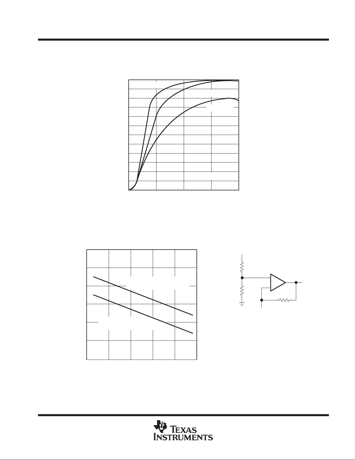
OUTPUT SINK CURRENT
vs
COLLECTOR OUTPUT SATURATION VOLTAGE
120
TA = –20°C
110
100
90
80
70
60
50
40
Output Sink Current – mA
30
20
10
0
0510
Collector Output Saturation Voltage – V
TA = 25°C
TA = 85°C
VCC = 3.6 V
15 20
TL1451A
SLVS024E – FEBRUARY 1983 – REVISED NOVEMBER 1999
– Maximum Output Voltage Swing – VV
V
V
V
V
V
V
OM
V
O(ref)
O(ref)
O(ref)
O(ref)
O(ref)
O(ref)
O(ref)
MAXIMUM OUTPUT VOLTAGE SWING
vs
FREE-AIR TEMPERATURE
–0.01
–0.02
Maximum Output Voltage
–0.03
–0.04
–0.05
–0.06
–0.07
–25 0 25 50 75 100
Maximum Output
Voltage Swing (Right Scale)
TA – Free-Air Temperature – °C
Swing (Right Scale)
Figure 22
1
0.9
0.8
0.7
0.6
0.5
– Maximum Output Voltage Swing – VV
OM
V
ref
33 kΩ
+
vom – 1
= 1.25 V
–
100 kΩ
R
L
33 kΩ
V
VCC = 3.6 V
RL = 100 kΩ
V
OM+1
VOM –1 = 1.15 V (Right Scale)
VOM –1 = 1.35 V (Left Scale)
TEST CIRCUIT
Figure 23
POST OFFICE BOX 655303 • DALLAS, TEXAS 75265
19
Page 20

TL1451A
DUAL PULSE-WIDTH-MODULATION CONTROL CIRCUITS
SLVS024E – FEBRUARY 1983 – REVISED NOVEMBER 1999
TYPICAL CHARACTERISTICS
OUTPUT TRANSISTOR ON DUTY CYCLE
DEAD-TIME INPUT VOLTAGE
0
VCC = 3.6 V
10
RT = 10kΩ
CT = 330 pF
20
30
40
50
60
70
80
Output Transistor “On” Duty Cycle – %
90
100
0 0.5 1 1.5 2 2.5 3
Dead-Time Input Voltage – V
Figure 24 Figure 25
vs
3.5 4
STANDBY CURRENT
vs
SUPPLY VOLTAGE
TA = 25°C
2
1.75
1.5
1.25
1
0.75
0.5
CC
ICC (Standby) – Standby Current – mA
I
0.25
0
01020
VCC – Supply Voltage – V
30 40
STANDBY CURRENT
FREE-AIR TEMPERATURE
2
1.75
1.5
1.25
1
0.75
CC
I
ICC – Supply Current – mA
0.5
0.25
0
–25 0 25 50
Average Supply Current
VCC = 6 V, RT = 10 kΩ,
CT = 330 pF
Stand-By Current, VCC = 40 V, No Load
Stand-By Current, VCC = 3.6 V, No Load
TA – Free-Air Temperature – °C
Figure 26 Figure 27
vs
75 100
MAXIMUM CONTINUOUS POWER DISSIPATION
vs
FREE-AIR TEMPERATURE
1200
1100
1000
Maximum Continuous Power Dissipation – mW
16-Pin N Plastic Dip
900
800
700
600
16-Pin NS Plastic SO
500
400
300
200
100
0
–25 0 25 50
Thermal Resistance
TA – Free-Air Temperature
Thermal Resistance
125°C/W
250°C/W
75 100
20
POST OFFICE BOX 655303 • DALLAS, TEXAS 75265
Page 21

TL1451A
DUAL PULSE-WIDTH-MODULATION CONTROL CIRCUITS
SLVS024E – FEBRUARY 1983 – REVISED NOVEMBER 1999
APPLICATION INFORMATION
V
CC
220 kΩ
470 Ω
150 Ω
L1
0.47 µF
V
C5
50 kΩ
ref
33 kΩ
33 kΩ
33 kΩ
R5
R2
C1
500 pF
TL1451A
33 kΩ
R1
500
pF
910111213141516
87654321
470 Ω
470 Ω
33 kΩ
33 kΩ
330 pF
220 Ω
470 Ω
1 µF
L2
R6
R7
R3
R4
C2
C4
Step-Up
Output
Step-Down
Output
NOTE A: V alues for R1 through R7, C1 through C4, and L1 and L2 depend upon individual application.
Figure 28. High-Speed Dual Switching Regulator
POST OFFICE BOX 655303 • DALLAS, TEXAS 75265
21
Page 22

TL1451A
DUAL PULSE-WIDTH-MODULATION CONTROL CIRCUITS
SLVS024E – FEBRUARY 1983 – REVISED NOVEMBER 1999
MECHANICAL DATA
D (R-PDSO-G**) PLASTIC SMALL-OUTLINE PACKAGE
14 PINS SHOWN
0.050 (1,27)
14
1
0.069 (1,75) MAX
0.020 (0,51)
0.014 (0,35)
8
7
A
0.010 (0,25)
0.004 (0,10)
DIM
0.157 (4,00)
0.150 (3,81)
PINS **
0.010 (0,25)
0.244 (6,20)
0.228 (5,80)
8
M
Seating Plane
0.004 (0,10)
14
0.008 (0,20) NOM
0°–8°
16
Gage Plane
0.010 (0,25)
0.044 (1,12)
0.016 (0,40)
A MAX
A MIN
NOTES: A. All linear dimensions are in inches (millimeters).
22
B. This drawing is subject to change without notice.
C. Body dimensions do not include mold flash or protrusion, not to exceed 0.006 (0,15).
D. Falls within JEDEC MS-012
POST OFFICE BOX 655303 • DALLAS, TEXAS 75265
0.197
(5,00)
0.189
(4,80)
0.344
(8,75)
0.337
(8,55)
0.394
(10,00)
0.386
(9,80)
4040047/D 10/96
Page 23
TL1451A
DUAL PULSE-WIDTH-MODULATION CONTROL CIRCUITS
SLVS024E – FEBRUARY 1983 – REVISED NOVEMBER 1999
MECHANICAL DATA
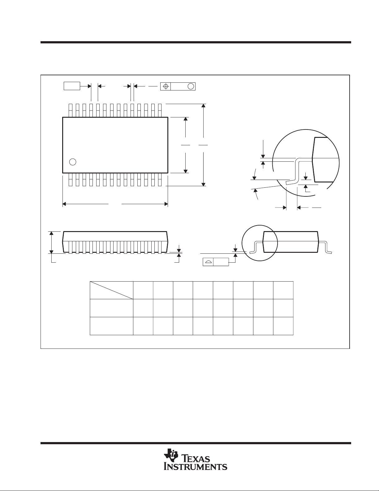
DB (R-PDSO-G**) PLASTIC SMALL-OUTLINE PACKAGE
28 PINS SHOWN
0,65
28
1
2,00 MAX
0,38
0,22
15
14
A
0,05 MIN
0,15
5,60
5,00
M
8,20
7,40
Seating Plane
0,10
0,15 NOM
Gage Plane
0°–8°
0,25
1,03
0,63
PINS **
DIM
A MAX
A MIN
NOTES: A. All linear dimensions are in millimeters.
B. This drawing is subject to change without notice.
C. Body dimensions do not include mold flash or protrusion not to exceed 0,15.
D. Falls within JEDEC MO-150
8
3,30
2,70
14
6,50
6,50
5,905,90
2016
7,50
6,90
24
8,50
28
10,50
9,907,90
30
10,50
9,90
38
12,90
12,30
4040065 /C 10/95
POST OFFICE BOX 655303 • DALLAS, TEXAS 75265
23
Page 24

TL1451A
DUAL PULSE-WIDTH-MODULATION CONTROL CIRCUITS
SLVS024E – FEBRUARY 1983 – REVISED NOVEMBER 1999
MECHANICAL DATA
FK (S-CQCC-N**) LEADLESS CERAMIC CHIP CARRIER
28 TERMINALS SHOWN
A SQ
B SQ
20
22
23
24
25
19
21
12826 27
12
1314151618 17
0.020 (0,51)
0.010 (0,25)
MIN
0.342
(8,69)
0.442
0.640
0.740
0.938
1.141
A
0.358
(9,09)
0.458
(11,63)
0.660
(16,76)
0.761
(19,32)(18,78)
0.962
(24,43)
1.165
(29,59)
NO. OF
TERMINALS
**
11
10
9
8
7
6
5
432
20
28
44
52
68
84
0.020 (0,51)
0.010 (0,25)
(11,23)
(16,26)
(23,83)
(28,99)
MINMAX
0.307
(7,80)
0.406
(10,31)
0.495
(12,58)
0.495
(12,58)
0.850
(21,6)
1.047
(26,6)
0.080 (2,03)
0.064 (1,63)
B
MAX
0.358
(9,09)
0.458
(11,63)
0.560
(14,22)
0.560
(14,22)
0.858
(21,8)
1.063
(27,0)
0.055 (1,40)
0.045 (1,14)
0.028 (0,71)
0.022 (0,54)
0.050 (1,27)
NOTES: A. All linear dimensions are in inches (millimeters).
24
B. This drawing is subject to change without notice.
C. This package can be hermetically sealed with a metal lid.
D. The terminals are gold-plated.
E. Falls within JEDEC MS-004
POST OFFICE BOX 655303 • DALLAS, TEXAS 75265
0.045 (1,14)
0.035 (0,89)
0.045 (1,14)
0.035 (0,89)
4040140/C 11/95
Page 25
TL1451A
DUAL PULSE-WIDTH-MODULATION CONTROL CIRCUITS
SLVS024E – FEBRUARY 1983 – REVISED NOVEMBER 1999
MECHANICAL DATA
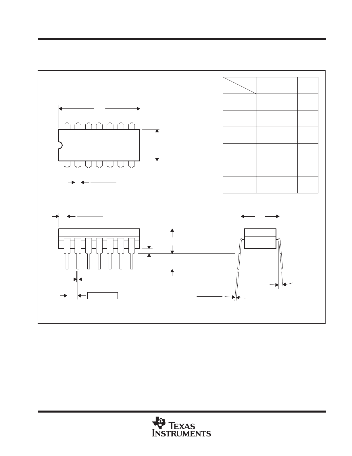
J (R-GDIP-T**) CERAMIC DUAL-IN-LINE
14 LEADS SHOWN
14
1
0.065 (1,65)
0.045 (1,14)
0.100 (2,54)
0.070 (1,78)
PINS **
DIM
A MAX
B
8
C
7
0.020 (0,51) MIN
0.200 (5,08) MAX
Seating Plane
A MIN
B MAX
B MIN
C MAX
C MIN
0.310
(7,87)
0.290
(7,37)
0.785
(19,94)
0.755
(19,18)
0.300A0.300
(7,62)
0.245
(6,22)
1614
0.310
(7,87)
0.290
(7,37)
0.785
(19,94)
0.755
(19,18)
(7,62)
0.245
(6,22)
20
0.310
(7,87)
0.290
(7,37)
0.975
(24,77)
0.930
(23,62)
0.300
(7,62)
0.245
(6,22)
0.023 (0,58)
0.015 (0,38)
0.100 (2,54)
NOTES: A. All linear dimensions are in inches (millimeters).
B. This drawing is subject to change without notice.
C. This package is hermetically sealed with a ceramic lid using glass frit.
D. Index point is provided on cap for terminal identification.
E. Falls within MIL STD 1835 GDIP1-T14, GDIP1-T16, and GDIP1-T20
0.130 (3,30) MIN
0°–15°
0.014 (0,36)
0.008 (0,20)
4040083/E 03/99
POST OFFICE BOX 655303 • DALLAS, TEXAS 75265
25
Page 26

TL1451A
DUAL PULSE-WIDTH-MODULATION CONTROL CIRCUITS
SLVS024E – FEBRUARY 1983 – REVISED NOVEMBER 1999
MECHANICAL DATA
N (R-PDIP-T**) PLASTIC DUAL-IN-LINE PACKAGE
16 PINS SHOWN
16
1
0.035 (0,89) MAX
PINS **
DIM
A
9
0.260 (6,60)
0.240 (6,10)
8
0.070 (1,78) MAX
0.020 (0,51) MIN
0.200 (5,08) MAX
A MAX
A MIN
Seating Plane
14
0.775
(19,69)
0.745
(18,92)
16
0.775
(19,69)
0.745
(18,92)
18
0.920
(23,37)
0.850
(21,59)
20
0.975
(24,77)
0.940
(23,88)
0.310 (7,87)
0.290 (7,37)
0.100 (2,54)
0.021 (0,53)
0.015 (0,38)
NOTES: A. All linear dimensions are in inches (millimeters).
B. This drawing is subject to change without notice.
C. Falls within JEDEC MS-001 (20-pin package is shorter than MS-001).
0.010 (0,25)
M
0.125 (3,18) MIN
0°–15°
0.010 (0,25) NOM
14/18 PIN ONL Y
4040049/C 08/95
26
POST OFFICE BOX 655303 • DALLAS, TEXAS 75265
Page 27

TL1451A
DUAL PULSE-WIDTH-MODULATION CONTROL CIRCUITS
SLVS024E – FEBRUARY 1983 – REVISED NOVEMBER 1999
MECHANICAL DATA
NS (R-PDSO-G**) PLASTIC SMALL-OUTLINE PACKAGE
14 PINS SHOWN
1,27
14
1
2,00 MAX
0,51
0,35
8
5,60
5,00
7
A
0,05 MIN
M
0,25
8,20
7,40
Seating Plane
0,10
0,15 NOM
Gage Plane
0°–10°
0,25
1,05
0,55
DIM
A MAX
NOTES: A. All linear dimensions are in millimeters.
B. This drawing is subject to change without notice.
C. Body dimensions do not include mold flash or protrusion, not to exceed 0,15.
PINS **
A MIN
16
10,501410,50
9,90 9,90
20 24
15,3012,90
12,30 14,70
4040062/B 02/95
POST OFFICE BOX 655303 • DALLAS, TEXAS 75265
27
Page 28

TL1451A
DUAL PULSE-WIDTH-MODULATION CONTROL CIRCUITS
SLVS024E – FEBRUARY 1983 – REVISED NOVEMBER 1999
MECHANICAL DATA
PW (R-PDSO-G**) PLASTIC SMALL-OUTLINE PACKAGE
14 PINS SHOWN
0,65
1,20 MAX
14
0,30
0,19
8
4,50
4,30
PINS **
7
Seating Plane
0,15
0,05
8
1
A
DIM
14
0,10
6,60
6,20
0,10
M
0,15 NOM
Gage Plane
0,25
0°–8°
2016
24
28
0,75
0,50
A MAX
A MIN
NOTES: A. All linear dimensions are in millimeters.
B. This drawing is subject to change without notice.
C. Body dimensions do not include mold flash or protrusion not to exceed 0,15.
D. Falls within JEDEC MO-153
3,10
2,90
5,10
4,90
5,10
4,90
6,60
6,40
7,90
7,70
9,80
9,60
4040064/F 01/97
28
POST OFFICE BOX 655303 • DALLAS, TEXAS 75265
Page 29

IMPORTANT NOTICE
T exas Instruments and its subsidiaries (TI) reserve the right to make changes to their products or to discontinue
any product or service without notice, and advise customers to obtain the latest version of relevant information
to verify, before placing orders, that information being relied on is current and complete. All products are sold
subject to the terms and conditions of sale supplied at the time of order acknowledgement, including those
pertaining to warranty, patent infringement, and limitation of liability.
TI warrants performance of its semiconductor products to the specifications applicable at the time of sale in
accordance with TI’s standard warranty. Testing and other quality control techniques are utilized to the extent
TI deems necessary to support this warranty . Specific testing of all parameters of each device is not necessarily
performed, except those mandated by government requirements.
CERTAIN APPLICATIONS USING SEMICONDUCTOR PRODUCTS MAY INVOLVE POTENTIAL RISKS OF
DEATH, PERSONAL INJURY, OR SEVERE PROPERTY OR ENVIRONMENTAL DAMAGE (“CRITICAL
APPLICATIONS”). TI SEMICONDUCTOR PRODUCTS ARE NOT DESIGNED, AUTHORIZED, OR
WARRANTED TO BE SUITABLE FOR USE IN LIFE-SUPPORT DEVICES OR SYSTEMS OR OTHER
CRITICAL APPLICA TIONS. INCLUSION OF TI PRODUCTS IN SUCH APPLICATIONS IS UNDERST OOD TO
BE FULLY AT THE CUSTOMER’S RISK.
In order to minimize risks associated with the customer’s applications, adequate design and operating
safeguards must be provided by the customer to minimize inherent or procedural hazards.
TI assumes no liability for applications assistance or customer product design. TI does not warrant or represent
that any license, either express or implied, is granted under any patent right, copyright, mask work right, or other
intellectual property right of TI covering or relating to any combination, machine, or process in which such
semiconductor products or services might be or are used. TI’s publication of information regarding any third
party’s products or services does not constitute TI’s approval, warranty or endorsement thereof.
Copyright 1999, Texas Instruments Incorporated
 Loading...