

查询TL1431供应商
TL1431
PRECISION PROGRAMMABLE REFERENCE
SLVS062F – DECEMBER 1991 – REVISED JANUAR Y 2000
D
0.4% Initial Voltage Tolerance
D
0.2-Ω Typical Output Impedance
D
Fast Turnon . . . 500 ns
D
Sink Current Capability ...1 mA to 100 mA
D
Low Reference Current (REF)
D
Adjustable Output Voltage ...V
I(ref)
description
The TL1431 is a precision programmable
reference with specified thermal stability over
automotive, commercial, and military
temperature ranges. The output voltage can be
set to any value between V
2.5 V) and 36 V with two external resistors (see
Figure 16). This device has a typical output
impedance of 0.2 Ω. Active output circuitry
provides a very sharp turnon characteristic,
making the device an excellent replacement for
zener diodes and other types of references in
applications such as onboard regulation,
adjustable power supplies, and switching power
supplies.
The TL1431C is characterized for operation over
the commercial temperature range of 0°C to
70°C. The TL1431Q is characterized for
operation over the full automotive temperature
range of –40°C to 125°C. The TL1431M is
characterized for operation over the full military
temperature range of –55°C to 125°C.
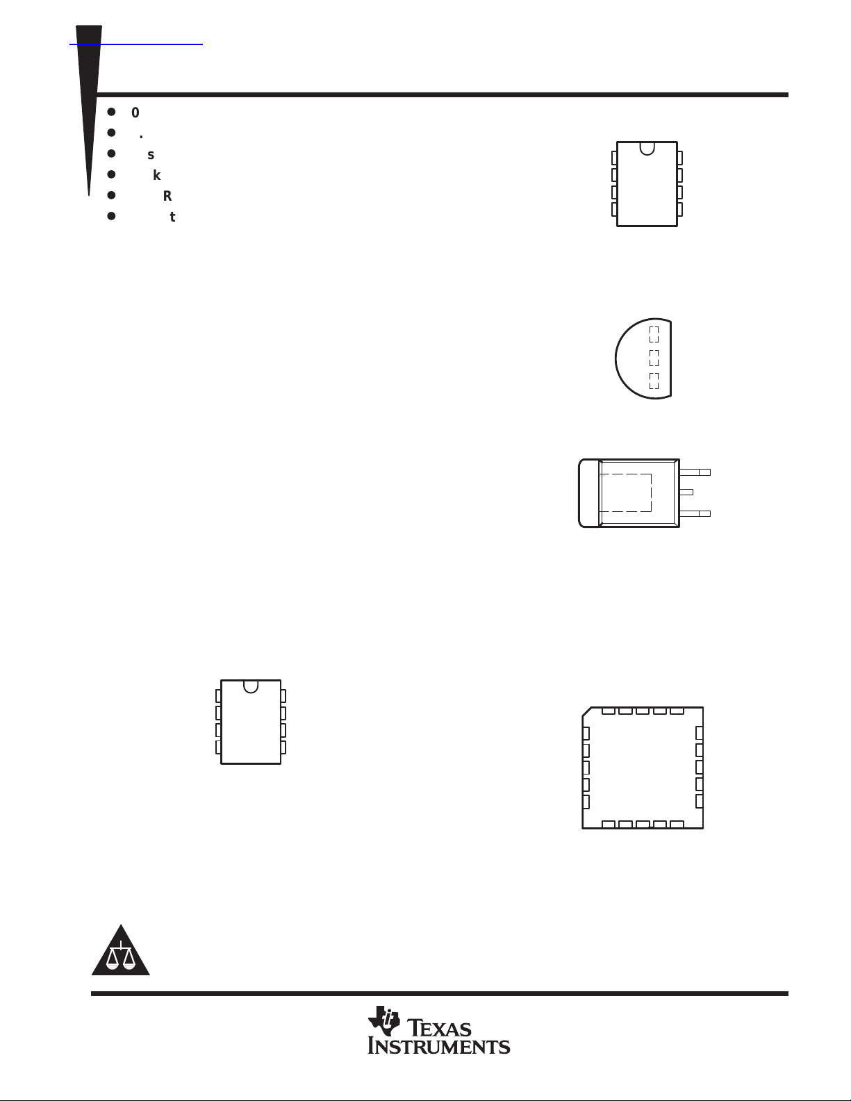
JG PACKAGE
(TOP VIEW)
(approximately
I(ref)
to 36 V
D PACKAGE
(TOP VIEW)
CATHODE
ANODE
ANODE
NC – No internal connection
ANODE terminals are connected internally.
1
2
3
NC
4
LP PACKAGE
(TOP VIEW)
8
7
6
5
REF
ANODE
ANODE
NC
CATHODE
ANODE
REF
KTP PACKAGE
(TOP VIEW)
CATHODE
ANODE
ANODE
REF
The ANODE terminal is in electrical contact with the
mounting base.
FK PACKAGE
(TOP VIEW)
CATHODE
NC – No internal connection
Please be aware that an important notice concerning availability, standard warranty, and use in critical applications of
Texas Instruments semiconductor products and disclaimers thereto appears at the end of this data sheet.
PRODUCTION DATA information is current as of publication date.
Products conform to specifications per the terms of Texas Instruments
standard warranty. Production processing does not necessarily include
testing of all parameters.
NC
NC
NC
1
2
3
4
8
7
6
5
REF
NC
ANODE
NC
POST OFFICE BOX 655303 • DALLAS, TEXAS 75265
NC
CATHODE
NC
REF
NC
NC
NC
NC
NC
NC
3212019
4
5
6
7
8
910111213
NCNCNC
Copyright 2000, Texas Instruments Incorporated
On products compliant to MIL-PRF-38535, all parameters are tested
unless otherwise noted. On all other products, production
processing does not necessarily include testing of all parameters.
NC
18
17
16
15
14
NC
NC
NC
NC
ANODE
NC
1
TL1431
PRECISION PROGRAMMABLE REFERENCE
SLVS062F – DECEMBER 1991 – REVISED JANUAR Y 2000
AVAILABLE OPTIONS
PACKAGED DEVICES
PLASTIC
FLANGE
MOUNTED
(KTP)
0°C to 70°C TL1431CD TL1431CKTPR TL1431CLP – –
–40°C to 125°C TL1431QD – TL1431QLP – –
–55°C to 125°C – – – TL1431MFK TL1431MJG
The D and LP packages are available taped and reeled. The KTP package is only available taped and reeled. Add the suffix R
to the device type (e.g., TL1431CDR). Chip forms are tested at 25°C.
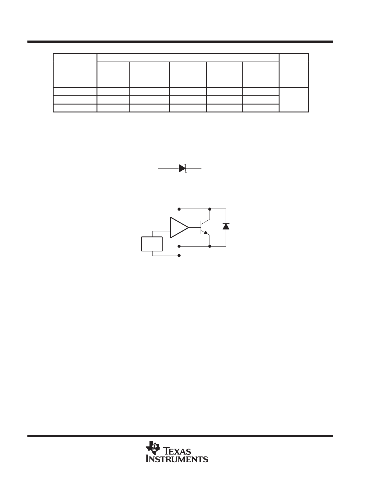
logic symbol
T
A
SMALL
OUTLINE
(D)
TO-226AA
(LP)
REF
CHIP
CARRIER
(FK)
CERAMIC
DIP
(JG)
CHIP
FORM
(Y)
TL1431Y
functional block diagram
REF
ANODE
V
ref
CATHODE
CATHODE
+
–
ANODE
2
POST OFFICE BOX 655303 • DALLAS, TEXAS 75265
TL1431
PRECISION PROGRAMMABLE REFERENCE
SLVS062F – DECEMBER 1991 – REVISED JANUAR Y 2000
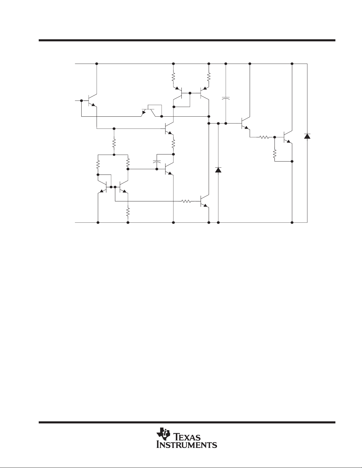
equivalent schematic
REF
1
8
2.4 kΩ
2,3,6,7
CATHODE
ANODE
†
3.28 kΩ
7.2 kΩ
20 pF
800 Ω
800 Ω
800 Ω
20 pF
150 Ω
4 kΩ
10 kΩ
1 kΩ
†
All component values are nominal.
Pin numbers shown are for the D package.
POST OFFICE BOX 655303 • DALLAS, TEXAS 75265
3
TL1431
PRECISION PROGRAMMABLE REFERENCE
SLVS062F – DECEMBER 1991 – REVISED JANUAR Y 2000
absolute maximum ratings over operating free-air temperature range (unless otherwise noted)
Cathode voltage,VKA (see Note 1) 37 V. . . . . . . . . . . . . . . . . . . . . . . . . . . . . . . . . . . . . . . . . . . . . . . . . . . . . . . . . . .
Continuous cathode current range, IKA –100 mA to 150 mA. . . . . . . . . . . . . . . . . . . . . . . . . . . . . . . . . . . . . . . . .
Reference input current range, I
Package thermal impedance, θJA (see Notes 2 and 3): D package 97°C/W. . . . . . . . . . . . . . . . . . . . . . . . . . . .
Lead temperature 1,6 mm (1/16 inch) from case for 10 seconds 260°C. . . . . . . . . . . . . . . . . . . . . . . . . . . . . . .
Storage temperature range, T
†
Stresses beyond those listed under “absolute maximum ratings” may cause permanent damage to the device. These are stress ratings only, and
functional operation of the device at these or any other conditions beyond those indicated under “recommended operating conditions” is not implied.
Exposure to absolute-maximum-rated conditions for extended periods may affect device reliability.
NOTES: 1. All voltage values are with respect to ANODE unless otherwise noted.
2. Maximum power dissipation is a function of TJ(max),
temperature is PD = (TJ(max) – TA)/
3. The package thermal impedance is calculated in accordance with JESD 51.
PACKAGE
FK 1375 mW 11.0 mW/°C 880 mW 715 mW 275 mW
JG 1050 mW 8.4 mW/°C 672 mW 546 mW 210 mW
TA = 25°C
POWER RATING
stg
POWER DISSIPATION RATING TABLE – FREE-AIR TEMPERATURE
–50 µA to 10 mA. . . . . . . . . . . . . . . . . . . . . . . . . . . . . . . . . . . . . . . . . . . . . . .
I(ref)
KTP package 28°C/W. . . . . . . . . . . . . . . . . . . . . . . . .
LP package 156°C/W. . . . . . . . . . . . . . . . . . . . . . . . . .
–65°C to 150°C. . . . . . . . . . . . . . . . . . . . . . . . . . . . . . . . . . . . . . . . . . . . . . . . . . .
θ
, and TA. The maximum allowable power dissipation at any allowable ambient
θ
. Operating at the absolute maximum TJ of 150°C can impact reliability.
JA
DERATING
FACTOR ABOVE
TA = 25°C
JA
TA = 70°C
POWER RATING
TA = 85°C
POWER RATING
TA = 125°C
POWER RATING
†
recommended operating conditions
V
I
T
KA
KA
A
Cathode voltage V
Cathode current 1 100 mA
Operating free-air temperature
MIN MAX UNIT
I(ref)
TL1431C 0 70
TL1431Q
TL1431M –55 125
–40 125
36 V
°C
4
POST OFFICE BOX 655303 • DALLAS, TEXAS 75265
PARAMETER
TEST CONDITIONS
T
†
UNIT
Reference
Reference
Off-state
TL1431
PRECISION PROGRAMMABLE REFERENCE
SLVS062F – DECEMBER 1991 – REVISED JANUAR Y 2000
electrical characteristics at specified free-air temperature, IKA = 10 mA (unless otherwise noted)
A
25°C 2490 2500 2510
V
I(ref)
V
I(dev)
D
D
I
I(ref)
I
I(dev)
I
off
|zKA|
†
Full range is 0°C to 70°C for C-suffix devices.
‡
The deviation parameters V
temperature range. The average full-range temperature coefficient of the reference input voltage
input voltage
Deviation of reference input
voltage over full temperature
‡
range
Ratio of change in reference
V
)
I(ref
input voltage to the change in
V
KA
cathode voltage
input current
Deviation of reference input
current over full temperature
‡
range
Minimum cathode current for
regulation
cathode current
Output impedance
ppm
ǒ
Ť
a
V
I(ref
where:
∆TA is the rated operating temperature range of the device.
Ǔ
Ť
+
°C
)
§
and I
I(dev)
V
)
I(dev
ǒ
V
I(ref
)
at 25
Ǔ
C
°
D
T
A
VKA = V
VKA = V
∆VKA = 3 V to 36 V
R1 = 10 kΩ,
R1 = 10 kΩ, R2 = ∞
VKA = V
VKA = 36 V,
VKA = V
IKA = 1 mA to 100 mA
are defined as the differences between the maximum and minimum values obtained over the rated
I(dev)
6
10
I(ref)
I(ref)
R2 = ∞
to 36 V 25°C Figure 1 0.45 1 mA
I(ref)
V
I(ref)
, f ≤ 1 kHz,
I(ref)
Max V
I(ref)
Full
range
Full
range
Full
range
25°C 1.5 2.5
Full
range
Full
range
25°C 0.18 0.5
= 0
Full
range
25°C Figure 1 0.2 0.4 Ω
TEST
CIRCUIT
Figure 1
Figure 1 4 20 mV
Figure 2 –1.1 –2 mV/V
Figure 2
Figure 2 0.2 1.2 µA
Figure 3
is defined as:
a
V
)
I(ref
TL1431C
MIN TYP MAX
2480 2520
mV
µA
3
µA
2
V
I(dev)
a
is positive or negative depending on whether minimum V
V
)
I(ref
§
The output impedance is defined as:
When the device is operating with two external resistors (see Figure 2), the total dynamic impedance of the circuit is given by: |z′|+
which is approximately equal to
Min V
I(ref)
∆T
A
or maximum V
I(ref)
D
V
Ť
z
KA
Ť
Ť
ǒ
z
1
KA
KA
Ť
+
D
I
KA
R1
Ǔ
)
.
R2
POST OFFICE BOX 655303 • DALLAS, TEXAS 75265
, respectively, occurs at the lower temperature.
I(ref)
D
V
,
D
I
5
TL1431
PARAMETER
TEST CONDITIONS
T
†
UNIT
Reference
Reference
Off-state
PRECISION PROGRAMMABLE REFERENCE
SLVS062F – DECEMBER 1991 – REVISED JANUAR Y 2000
electrical characteristics at specified free-air temperature, IKA = 10 mA (unless otherwise noted)
TEST
A
CIRCUIT
25°C 2490 2500 2510 2475 2500 2540
V
I(ref)
V
I(dev)
D
D
I
I(ref)
I
I(dev)
I
off
|zKA|
*On products compliant to MIL-PRF-38535, this parameter is not production tested.
†
Full range is –40°C to 125°C for Q-suffix devices, and –55°C to 125°C for M-suffix devices.
‡
The deviation parameters V
temperature range. The average full-range temperature coefficient of the reference input voltage
input voltage
Deviation of
reference input
voltage over full
temperature range
Ratio of change in
reference input
V
)
I(ref
voltage to the
V
KA
change in cathode
voltage
input current
Deviation of
reference input
current over full
temperature range
Minimum
cathode current
for regulation
cathode current
Output impedance
ǒ
ppm
ǒ
Ť
Ť
a
V
°C
)
I(ref
where:
∆TA is the rated operating temperature range of the device.
V
Ǔ
+
VKA = V
VKA = V
‡
∆VKA = 3 V to 36 V
R1 = 10 kΩ,
R1 = 10 kΩ, R2 = ∞
‡
VKA = V
VKA = 36 V,
VKA = V
§
IKA = 1 mA to 100 mA
and I
I(dev)
V
)
I(dev
Ǔ
C
at 25
°
)
I(ref
D
T
A
Figure 1
I(ref)
I(ref)
R2 = ∞
to 36 V 25°C Figure 1 0.45 1 0.45 1 mA
I(ref)
V
I(ref)
, f ≤ 1 kHz,
I(ref)
are defined as the differences between the maximum and minimum values obtained over the rated
I(dev)
6
10
Full
range
Full
range
range
range
range
= 0
range
Figure 1 17 55 17 55* mV
Full
Figure 2 –1.1 –2 –1.1 –2 mV/V
25°C 1.5 2.5 1.5 2.5
Figure 2
Full
Full
Figure 2 0.5 2 0.5 3* µA
25°C 0.18 0.5 0.18 0.5
Figure 3
Full
25°C Figure 1 0.2 0.4 0.2 0.4 Ω
Max V
I(ref)
TL1431Q TL1431M
MIN TYP MAX MIN TYP MAX
2470 2530 2460 2550
4 5
2 2
a
is defined as:
V
)
I(ref
mV
µA
µA
V
I(dev)
a
V
§
The output impedance is defined as:
When the device is operating with two external resistors (see Figure 2), the total dynamic impedance of the circuit is given by: |z′|+
which is approximately equal to
6
is positive or negative depending on whether minimum V
)
I(ref
D
V
Ť
z
KA
Ť
Ť
ǒ
z
1
KA
KA
Ť
+
D
I
KA
R1
Ǔ
)
.
R2
POST OFFICE BOX 655303 • DALLAS, TEXAS 75265
Min V
or maximum V
I(ref)
I(ref)
∆T
A
, respectively, occurs at the lower temperature.
I(ref)
D
V
,
D
I

PARAMETER
TEST CONDITIONS
UNIT
(
)
I(ref
)
gg
∆V
V
Figure 2
1–2
mV/V
PRECISION PROGRAMMABLE REFERENCE
SLVS062F – DECEMBER 1991 – REVISED JANUAR Y 2000
electrical characteristics at IKA = 10 mA, TA = 25°C
TEST
CIRCUIT
V
I(ref)
D
V
D
I
I(ref)
IKAmin Minimum cathode current for regulation VKA = V
I
off
|zKA| Output impedance
†
The output impedance is defined as: |z′|+
When the device is operating with two external resistors (see Figure 2), the total dynamic impedance of the circuit is given by: Ťz
which is approximately equal to
Reference input voltage VKA = V
Ratio of change in reference input voltage
to the change in cathode voltage
V
KA
Reference input current R1 = 10 kΩ, R2 = ∞ Figure 2 1.44 2.5 µA
Off-state cathode current VKA = 36 V, V
†
D
V
D
I
Ť
z
KA
R1
Ť
ǒ
Ǔ
1
)
.
R2
VKA = V
IKA = 1 mA to 100 mA
I(ref)
= 3 V to 36
KA
I(ref)
I(ref)
to 36 V Figure 1 0.45 1 mA
= 0 Figure 3 0.18 0.5 µA
ref
, f ≤ 1 kHz,
Figure 1 2490 2500 2510 mV
Figure 1 0.2 0.4 Ω
TL1431Y
MIN TYP MAX
–1.
TL1431
D
Ť
+
KA
D
V
KA
,
I
KA
PARAMETER MEASUREMENT INFORMATION
V
)
I(dev
ǒ
V
at 25
°
)
ppm
ǒ
Ť
Ť
a
V
°C
)
I(ref
where:
∆TA is the rated operating temperature range of the device.
Input
I(ref
Ǔ
+
V
I(ref)
D
T
A
Figure 1. Test Circuit for V
6
Ǔ
10
C
V
KA
I
KA
= V
(KA)
ref
Max V
Min V
Input
I(ref)
I(ref)
I
R1
R2
I
I(ref)
V
I(ref)
KA
VKA+
Figure 2. Test Circuit for V
∆T
V
A
V
I(ref)
KA
V
I(dev)
R1
ǒ
1
)
(KA)
R2
Ǔ
)
> V
I
I(ref)
ref
R1
POST OFFICE BOX 655303 • DALLAS, TEXAS 75265
7
TL1431
PRECISION PROGRAMMABLE REFERENCE
SLVS062F – DECEMBER 1991 – REVISED JANUAR Y 2000
PARAMETER MEASUREMENT INFORMATION
Input
I
off
Figure 3. Test Circuit for I
V
KA
off
TYPICAL CHARACTERISTICS
Table of Graphs
FIGURE
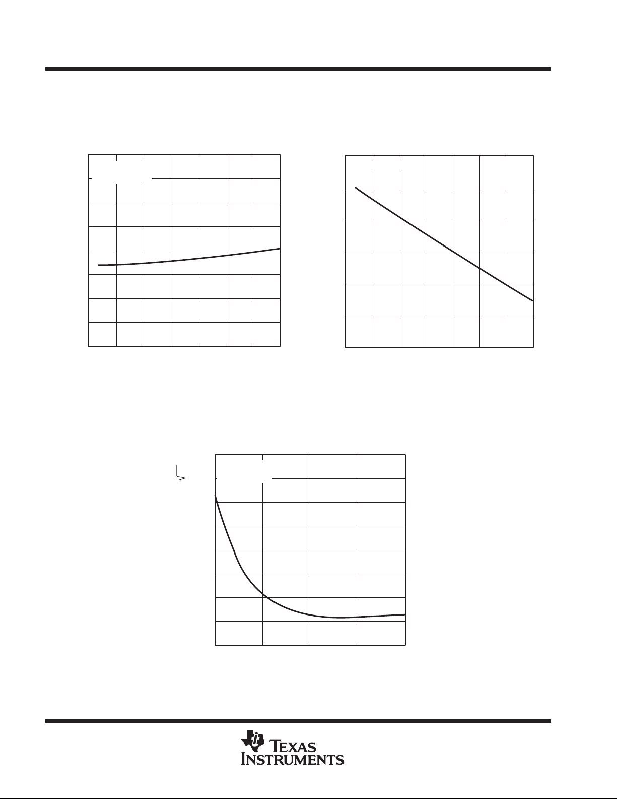
Reference voltage vs Free-air temperature 4
Reference current vs Free-air temperature 5
Cathode current vs Cathode voltage 6, 7
Off-state cathode current vs Free-air temperature 8
Ratio of delta reference voltage to delta cathode voltage vs Free-air temperature 9
Equivalent input-noise voltage vs Frequency 10
Equivalent input-noise voltage over a 10-second period 11
Small-signal voltage amplification vs Frequency 12
Reference impedance vs Frequency 13
Pulse response 14
Stability boundary conditions 15
8
POST OFFICE BOX 655303 • DALLAS, TEXAS 75265
TL1431
PRECISION PROGRAMMABLE REFERENCE
SLVS062F – DECEMBER 1991 – REVISED JANUAR Y 2000
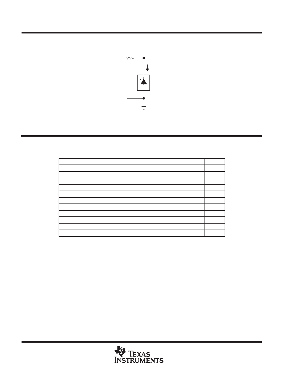
REFERENCE VOLTAGE
FREE-AIR TEMPERATURE
2.52
V
= V
I(ref)
IKA = 10 mA
2.51
2.5
– Reference Voltage – VV
I(ref)
2.49
2.48
– 50 – 25 0 25 50
KA
TA – Free-Air Temperature – °C
vs
Figure 4
TYPICAL CHARACTERISTICS
2.5
IKA = 10 mA
R1 = 10 kΩ
R2 = ∞
2
1.5
1
0.5
0
– 50 – 25 0 25 50 75 100 125
75 100 125
Aµ
– Reference Current –
I(ref)
I
†
REFERENCE CURRENT
vs
FREE-AIR TEMPERATURE
TA – Free-Air Temperature – °C
Figure 5
150
VKA = V
TA = 25°C
100
50
0
– 50
– Cathode Current – mAI
KA
– 100
– 150
– 3 – 2 – 1
CATHODE CURRENT
vs
CATHODE VOLTAGE
I(ref)
012
VKA – Cathode Voltage – V
Figure 6
CATHODE CURRENT
vs
CATHODE VOLTAGE
800
VKA = V
TA = 25°C
600
Aµ
400
200
– Cathode Current –I
KA
0
– 200
3
–2
I(ref)
–1 0 1 2 3 4
VKA – Cathode Voltage – V
Figure 7
†
Data at high and low temperatures are applicable only within the recommended operating free-air temperature ranges of the various devices.
POST OFFICE BOX 655303 • DALLAS, TEXAS 75265
9
TL1431
PRECISION PROGRAMMABLE REFERENCE
SLVS062F – DECEMBER 1991 – REVISED JANUAR Y 2000
OFF-STATE CATHODE CURRENT
FREE-AIR TEMPERATURE
0.4
0.35
0.3
0.25
0.2
0.15
0.1
0.05
0
–50
VKA = 36 V
V
= 0
I(ref)
– 25 0 25 50 75
TA – Free-Air Temperature – °C
Aµ
KA(off)
I – Off-State Cathode Current –
Figure 8
vs
TYPICAL CHARACTERISTICS
RATIO OF DELTA REFERENCE VOLTAGE TO
100 125
– mV/V∆V
KA
/∆V
I(ref)
–0.85
–0.95
–1.05
–1.15
–1.25
–1.35
–1.45
VKA = 3 V to 36 V
– 25 0
–50
†
DELTA CATHODE VOLTAGE
vs
FREE-AIR TEMPERATURE
25 50 75 100 125
TA – Free-Air Temperature – °C
Figure 9
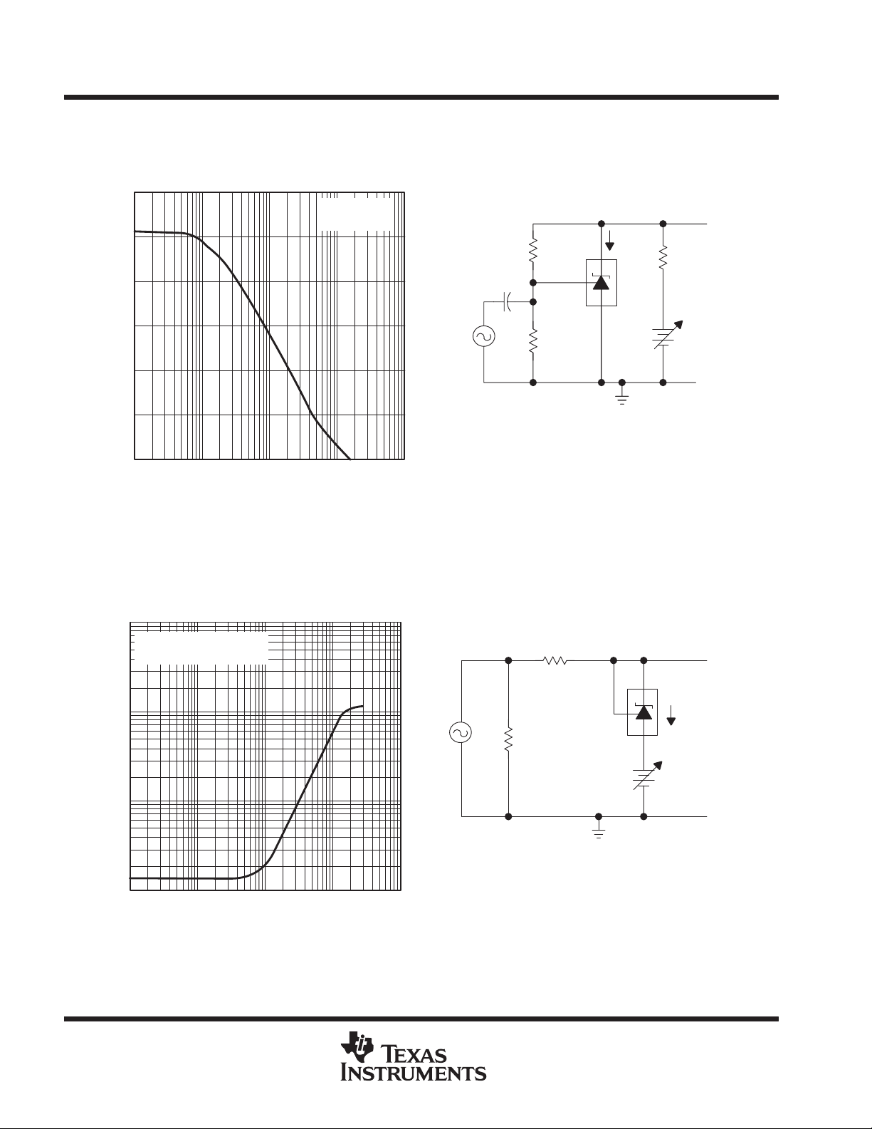
EQUIVALENT INPUT-NOISE VOLTAGE
vs
FREQUENCY
260
IO = 10 mA
TA = 25°C
240
220
200
180
160
140
120
– Equivalent Input Noise Voltage – nV/ HzV
n
100
10 100 1 k
f – Frequency – Hz
10 k 100 k
Figure 10
†
Data at high and low temperatures are applicable only within the recommended operating free-air temperature ranges of the various devices.
10
POST OFFICE BOX 655303 • DALLAS, TEXAS 75265

TL1431
PRECISION PROGRAMMABLE REFERENCE
SLVS062F – DECEMBER 1991 – REVISED JANUAR Y 2000
TYPICAL CHARACTERISTICS
EQUIVALENT INPUT-NOISE VOLTAGE
6
5
4
µV
3
2
1
0
– 1
– 2
– 3
– 4
– Equivalent Input Noise Voltage –
n
– 5
V
– 6
OVER A 10-SECOND PERIOD
f = 0.1 to 10 Hz
IKA = 10 mA
TA = 25°C
0246
t – Time – s
810
500 µF
910 Ω
19.1 V
1 kΩ
TL1431
(DUT)
2000 µF
820 Ω
16 Ω
160 kΩ
0.1 µF
TEST CIRCUIT FOR 0.1-Hz TO 10-Hz EQUIVALENT INPUT-NOISE VOLTAGE
V
CC
TLE2027
AV = 10 V/mV
+
–
V
EE
16 Ω
16 Ω
1 µF
1 µF
33 kΩ
33 kΩ
V
CC
+
–
V
EE
Figure 11
TLE2027
AV = 2 V/V
2.2 µF
CRO
1 MΩ
POST OFFICE BOX 655303 • DALLAS, TEXAS 75265
11
TL1431
PRECISION PROGRAMMABLE REFERENCE
SLVS062F – DECEMBER 1991 – REVISED JANUAR Y 2000
TYPICAL CHARACTERISTICS
SMALL-SIGNAL VOLTAGE AMPLIFICATION
vs
FREQUENCY
60
IKA = 10 mA
TA = 25°C
50
15 kΩ
I
(K)
Output
230 Ω
40
30
20
10
– Small-Signal Voltage Amplification – dB
V
A
0
1 k 10 k 100 k
REFERENCE IMPEDANCE
100
IKA = 1 mA to 100 mA
TA = 25°C
Ω
10
f – Frequency – Hz
vs
FREQUENCY
1 M 10 M
Figure 12
9 µF
+
8.25 kΩ
–
GND
TEST CIRCUIT FOR VOLTAGE AMPLIFICATION
1 kΩ
I
(K)
Output
1
KA
|z
|zka | – Reference Impedance – O
0.1
1 k 10 k 100 k 1 M 10 M
12
50 Ω
–
+
GND
TEST CIRCUIT FOR REFERENCE IMPEDANCE
f – Frequency – Hz
Figure 13
POST OFFICE BOX 655303 • DALLAS, TEXAS 75265
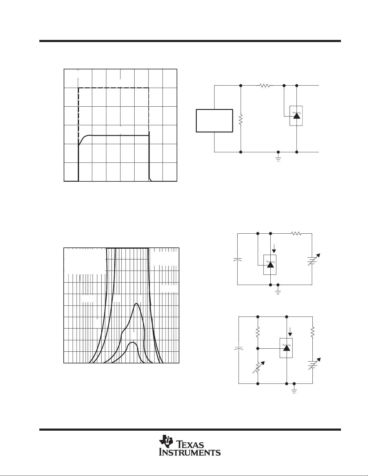
Input and Output Voltages – V
6
5
4
3
2
1
TA = 25°C
PULSE RESPONSE
Input
Output
PRECISION PROGRAMMABLE REFERENCE
SLVS062F – DECEMBER 1991 – REVISED JANUAR Y 2000
TYPICAL CHARACTERISTICS
Pulse
Generator
f = 100 kHz
TEST CIRCUIT FOR PULSE RESPONSE
TL1431
V
I
50 Ω
220 Ω
Output
GND
0
01234
t – Time – µs
567
Figure 14
STABILITY BOUNDARY CONDITIONS
100
A-VKA = V
B-VKA = 5 V
90
C-VKA = 10 V
D-VKA = 15 V
80
70
60
50
40
– Cathode Current – mAI
30
KA
20
10
0
0.001 0.01 0.1 1
†
The areas under the curves represent conditions that may cause the
device to oscillate. For curves B, C, and D, R2 and V+ are adjusted to
establish the initial VKA and IKA conditions with CL = 0. V
are then adjusted to determine the ranges of stability.
I(ref)
Stable
A
CL – Load Capacitance – µF
B
D
C
†
IKA = 10 mA
TA = 25°C
Stable
and C
BATT
10
150 Ω
I
KA
C
L
TEST CIRCUIT FOR CURVE A
R1 =
10 kΩ
C
L
R2
L
TEST CIRCUIT FOR CURVES B, C, AND D
I
KA
V
I
+
V
BATT
–
150 Ω
V
I
+
V
BATT
–
Figure 15
POST OFFICE BOX 655303 • DALLAS, TEXAS 75265
13

TL1431
PRECISION PROGRAMMABLE REFERENCE
SLVS062F – DECEMBER 1991 – REVISED JANUAR Y 2000
APPLICATION INFORMATION
Table of Application Circuits
APPLICATION FIGURE
Shunt regulator 16
Single-supply comparator with temperature-compensated threshold 17
Precision high-current series regulator 18
Output control of a three-terminal fixed regulator 19
Higher-current shunt regulator 20
Crowbar 21
Precision 5-V , 1.5-A, 0.5% regulator 22
5-V precision regulator 23
PWM converter with 0.5% reference 24
Voltage monitor 25
Delay timer 26
Precision current limiter 27
Precision constant-current sink 28
V
(BATT)
NOTE A: R should provide cathode current ≥1 mA to the TL1431 at
minimum V
R
R1
0.1%
V
I(ref)
R2
0.1%
VO+
(BATT)
V
O
TL1431
R1
ǒ
.
Ǔ
1
)
V
I(ref)
R2
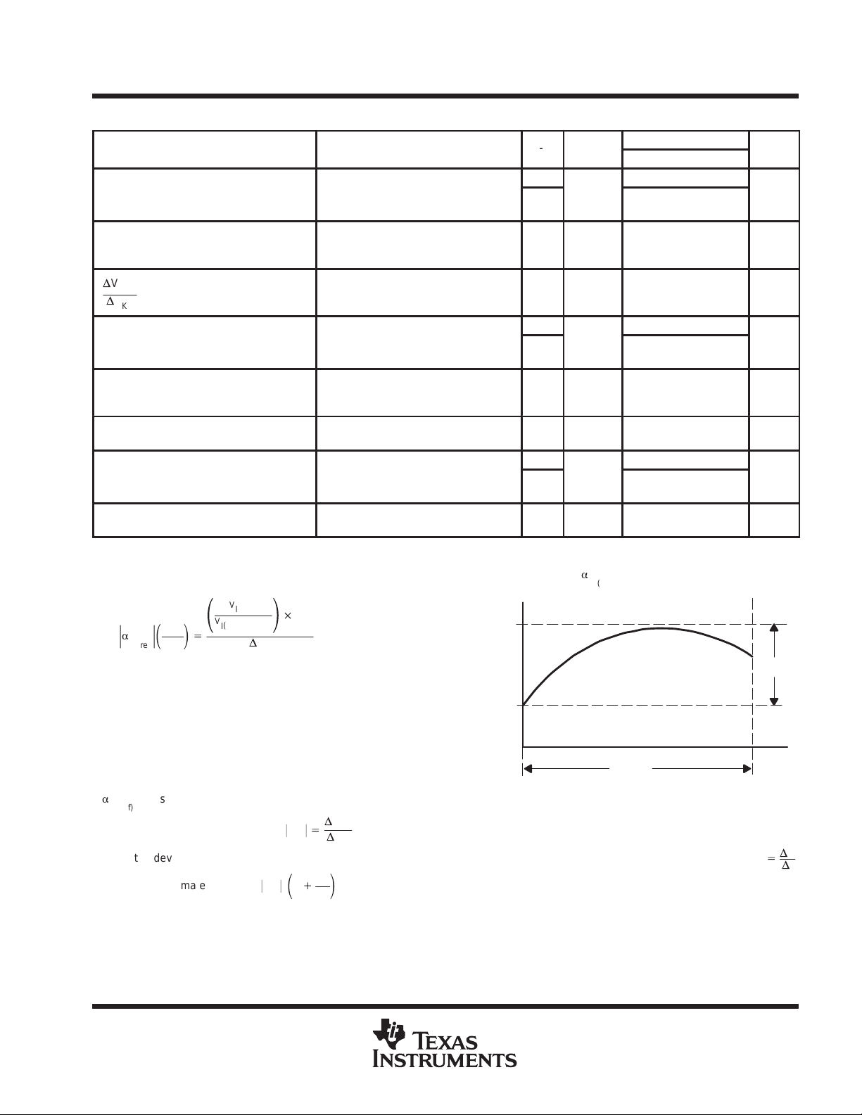
Figure 16. Shunt Regulator
V
(BATT)
V
O
Von ≈ 2 V
V
≈ V
off
(BATT)
Input
VIT = 2.5 V
TL1431
GND
Figure 17. Single-Supply Comparator
With Temperature-Compensated Threshold
14
POST OFFICE BOX 655303 • DALLAS, TEXAS 75265

TL1431
PRECISION PROGRAMMABLE REFERENCE
SLVS062F – DECEMBER 1991 – REVISED JANUAR Y 2000
APPLICATION INFORMATION
V
V
(BATT)
(BATT)
R
30 Ω
2N2222
2N2222
Common
µA7805
IN
OUT
R1
V
O
TL1431
NOTE A: R should provide cathode current ≥1 mA to the TL1431 at
minimum V
R2
0.1%
VO+
(BATT).
0.01 µF
ǒ
1
)
R1
0.1%
R1
R2
4.7 kΩ
V
O
Ǔ
V
I(ref)
Figure 18. Precision High-Current Series Regulator
V
(BATT)
R
R1
R2
TL1431
V
O
V
(BATT)
TL1431
V
Min V = V
+
R1
ǒ
Ǔ
1
)
R2
I(ref)
V
I(ref)
+ 5 V
R2
Figure 19. Output Control of a
Three-Terminal Fixed Regulator
R1
TL1431
C
R2
R1
trip
+
ǒ
V
Ǔ
1
)
V
I(ref)
R2
V
O
VO+
ǒ
Ǔ
1
)
V
I(ref)
R2
R1
Figure 20. Higher-Current Shunt Regulator
POST OFFICE BOX 655303 • DALLAS, TEXAS 75265
NOTE A: Refer to the stability boundary conditions in Figure 15 to
determine allowable values for C.
Figure 21. Crowbar
15

TL1431
PRECISION PROGRAMMABLE REFERENCE
SLVS062F – DECEMBER 1991 – REVISED JANUAR Y 2000
APPLICATION INFORMATION
V
(BATT)
In Out
LM317
8.2 kΩ
Adjust
TL1431
VO = 5 V, 1.5 A, 0.5%
243 Ω
0.1%
243 Ω
0.1%
V
(BATT) VO = 5 V
R
b
TL1431
NOTE A: Rb should provide cathode current ≥1 mA to the TL1431.
27.4 kΩ
0.1%
27.4 kΩ
0.1%
Figure 22. Precision 5-V, 1.5-A, 0.5% Regulator
6.8 kΩ
5 V +0.5%
TL1431
10 kΩ
10 kΩ
0.1%
10 kΩ
0.1%
Figure 24. PWM Converter With 0.5% Reference
Used
Feedback
Figure 23. 5-V Precision Regulator
12 V
V
CC
–
+
X
Not
TL598
16
POST OFFICE BOX 655303 • DALLAS, TEXAS 75265

TL1431
PRECISION PROGRAMMABLE REFERENCE
SLVS062F – DECEMBER 1991 – REVISED JANUAR Y 2000
APPLICATION INFORMATION
V
(BATT)
R1A
TL1431
R2A
R1B
Low Limit
High Limit
NOTE A: Select R3 and R4 to provide the desired LED intensity and
ǒ
+
1
ǒ
1
+
cathode current ≥1 mA to the TL1431.
)
)
R2B
R1A
R2A
Ǔ
V
I(ref)
V
I(ref)
Low Limit < V
Ǔ
R3
R1B
TL1431
R2B
LED on When
(BATT)
R4
< High Limit
Figure 25. Voltage Monitor
V
(BATT)
RCL 0.1%
R1
I
O
12 V
R
On
Off
Delay+R C I
Figure 26. Delay Timer
V
(BATT)
680 Ω
2 kΩ
C
I
(
12 V)*
TL1431
12 V
I
O
V
I(ref)
TL1431
V
I(ref)
IO+
R1
+
R
ǒ
h
CL
V
I
O
FE
)
I
(BATT)
Ǔ
)
KA
I
KA
Figure 27. Precision Current Limiter
TL1431
RS
0.1%
V
I(ref)
IO+
R
S
Figure 28. Precision Constant-Current Sink
POST OFFICE BOX 655303 • DALLAS, TEXAS 75265
17

IMPORTANT NOTICE
T exas Instruments and its subsidiaries (TI) reserve the right to make changes to their products or to discontinue
any product or service without notice, and advise customers to obtain the latest version of relevant information
to verify, before placing orders, that information being relied on is current and complete. All products are sold
subject to the terms and conditions of sale supplied at the time of order acknowledgement, including those
pertaining to warranty, patent infringement, and limitation of liability.
TI warrants performance of its semiconductor products to the specifications applicable at the time of sale in
accordance with TI’s standard warranty. Testing and other quality control techniques are utilized to the extent
TI deems necessary to support this warranty . Specific testing of all parameters of each device is not necessarily
performed, except those mandated by government requirements.
CERTAIN APPLICA TIONS USING SEMICONDUCTOR PRODUCTS MA Y INVOLVE POTENTIAL RISKS OF
DEATH, PERSONAL INJURY, OR SEVERE PROPERTY OR ENVIRONMENTAL DAMAGE (“CRITICAL
APPLICATIONS”). TI SEMICONDUCTOR PRODUCTS ARE NOT DESIGNED, AUTHORIZED, OR
WARRANTED TO BE SUITABLE FOR USE IN LIFE-SUPPORT DEVICES OR SYSTEMS OR OTHER
CRITICAL APPLICA TIONS. INCLUSION OF TI PRODUCTS IN SUCH APPLICATIONS IS UNDERST OOD TO
BE FULLY AT THE CUSTOMER’S RISK.
In order to minimize risks associated with the customer’s applications, adequate design and operating
safeguards must be provided by the customer to minimize inherent or procedural hazards.
TI assumes no liability for applications assistance or customer product design. TI does not warrant or represent
that any license, either express or implied, is granted under any patent right, copyright, mask work right, or other
intellectual property right of TI covering or relating to any combination, machine, or process in which such
semiconductor products or services might be or are used. TI’s publication of information regarding any third
party’s products or services does not constitute TI’s approval, warranty or endorsement thereof.
Copyright 2000, Texas Instruments Incorporated
 Loading...