

Page 1
查询TL1051供应商
TL1051
VIDEO PREPROCESSOR CIRCUIT
SOCS032B – NOVEMBER 1991
• Solid-State Reliability
• Supports Both Color and Monochrome
Applications
• Three Independent Channels Available for
Use With RGB Monitors
• Clamp Pulse-Select Option
• White-Clip Function for Y Signal
• Gain Control for R, G, B, and Y
• Noise Suppression During Video-Blanking
Periods
• Y Signal Generated From Three
Independent Channels
description
The TL1051 is a bipolar monolithic integrated circuit designed for use in preprocessing three channels of TI CCD
image sensors. It receives video inputs from the TI TL1593 three-channel sample-and-hold circuit and outputs
three processed channel signals and a single multiplexed Y (luminance) signal. Processing functions of the
TL1051 include gain, automatic gain control, clamp, white balance, and white clip.
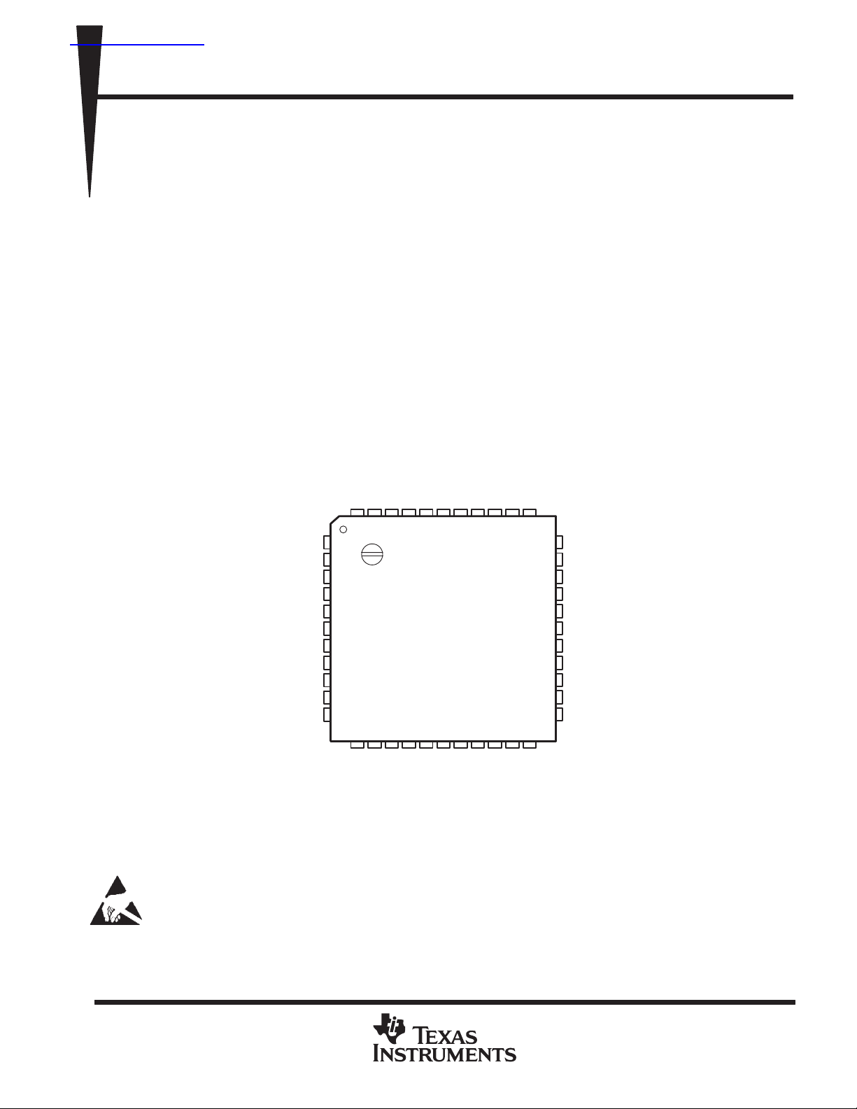
The TL1051 is supplied in a 44-pin surface-mount plastic package and is characterized for operation from –20°C
to 45°C.
FR PACKAGE
(TOP VIEW)
GND
ALCREF
AGCSET
RESET
ALCDRV
ALC–
ALC+
GATE
GATEOUT
GATEIN
AGCDET
43 42 41 40 3944 38
NC
1
WB
2
CONTB
CONTA
V
CLPLVLB
CLPLVLG
CLPLVLR
NC – No internal connection
This device contains circuits to protect its inputs and outputs against damage due to high static voltages or electrostatic fields. These
circuits have been qualified to protect this device against electrostatic discharges (ESD) of up to 2 kV according to MIL-STD-883C,
Method 3015; however, precautions should be taken to avoid application of any voltage higher than maximum-rated voltages to these
conductive foam. In a circuit, unused inputs should always be connected to an appropriate logic voltage level, preferably either VCC or ground.
Specific guidelines for handling devices of this type are contained in the publication
(ESDS) Devices and Assemblies
high-impedance circuits. During storage or handling, the device leads should be shorted together or the device should be placed in
available from Texas Instruments.
CC
BIN
GIN
RIN
3
4
5
6
7
8
9
10
11
12 13
GND
14 15 16 17
SWB
SWR
SWG
PBL
PCL1
36 35 3437
18 19 20 21 22
HL
YSW
PCL2
Y AGCIN
Guidelines for Handling Electrostatic-Discharge-Sensitive
33
32
31
30
29
28
27
26
25
24
23
Y AGC
AGCOUT
REF2V
AGCCONT
AGCLMT
BOUT
GOUT
ROUT
YOUT
Y ALC
WCPCONT
YCLAMP
PRODUCTION DATA information is current as of publication date.
Products conform to specifications per the terms of Texas Instruments
standard warranty. Production processing does not necessarily include
testing of all parameters.
POST OFFICE BOX 655303 • DALLAS, TEXAS 75265
Copyright 1991, Texas Instruments Incorporated
4-1
Page 2
TL1051
VIDEO PREPROCESSOR CIRCUIT
SOCS032B – NOVEMBER 1991
functional block diagram
41
+
ALC
ALC –
42
ALC
AMP
43
ALCDRV
RESET
GATE
GATE IN
AGCDET
AGCSET
CONTA
CONTB
AGCLMT
AGCCONT
WB
PCL2
YCLAMP
WCPCONT
YAGCIN
BIN
CLPLVLB
GIN
CLPLVLG
RIN
CLPLVLR
PCL1
PBL
44
40
38
34
35
4
3
30
31
2
18
23
24
21
6
9
7
10
8
11
16
17
Reset
Gate
AGC
AMP
A/D
Blue
Clamp
Green
Clamp
Red
Clamp
Blue
Blank
Green
Blank
Red
Blank
3 3
Clamp
Buffer
3
2
1
Blank
Buffer
White
Level
White
Level
AGC
CONT
YAGC
Blue
AGC
Green
AGC
Red
AGC
GATEOUT
39
33
AGCOUT
3
HLMIX
Y
Clamp
WCP-
CONT
ALC
REF
19
26
22
29
28
27
25
36
HL
YOUT
YAGC
BOUT
GOUT
ROUT
YALC
ALCREF
4-2
SWR
SWG
SWB
13
14
15
YSW
POST OFFICE BOX 655303 • DALLAS, TEXAS 75265
20
YSW
Page 3
VIDEO PREPROCESSOR CIRCUIT
I/O
DESCRIPTION
Terminal Functions
TERMINAL
NAME NO.
AGCCONT 31 I AGC control
AGCDET 34 I AGC detect
AGCLMT 30 I AGC limit
AGCOUT 33 O AGC out
AGCSET 35 I AGC set
ALCDRV 43 O ALC drive
ALCREF 36 O ALC reference
ALC+ 41 I ALC noninverting input
ALC– 42 I ALC inverting input
BIN 6 I Blue channel in
BOUT 29 O Blue channel out
CLPLVLB 9 I DC clamp level – blue
CLPLVLG 10 I DC clamp level – green
CLPLVLR 11 I DC clamp level – red
CONTA 4 I White balance digital control – A
CONTB 3 I White balance digital control – B
GATE 40 I Video gate control switch
GATEIN 38 I Video gate in
GATEOUT 39 O Video gate out
GIN 7 I Green channel in
GND 12, 37 Ground
GOUT 28 O Green channel out
HL 19 O Highlight suppression (not used)
NC 1 No internal connection
PBL 17 I Process blanking
PCL1 16 I Clamp signal 1
PCL2 18 I Clamp signal 2
REF2V 32 O 2-V reference
RESET 44 I Reset
RIN 8 I Red channel in
ROUT 27 O Red channel out
SWB 15 I Multiplex switch – blue
SWG 14 I Multiplex switch – green
SWR 13 I Multiplex switch – red
V
CC
WB 2 I White balance analog control
WCPCONT 24 I White clip control
YAGC 22 O YAGC out
YAGCIN 21 I Y AGC in
YALC 25 O Y automatic level control
YCLAMP 23 I Y clamp
YOUT 26 O Y signal out
YSW 20 O Multiplexed Y out
5 Power supply voltage
TL1051
SOCS032B – NOVEMBER 1991
POST OFFICE BOX 655303 • DALLAS, TEXAS 75265
4-3
Page 4
TL1051
VIDEO PREPROCESSOR CIRCUIT
SOCS032B – NOVEMBER 1991
detailed description
white-balance control
White balance in the monochrome mode can be adjusted with either terminal 2 (white-balance analog control)
or with terminals 3 and 4 (white-balance digital controls B and A, respectively). If analog control is selected,
terminals 3 and 4 should be left open and terminal 2 adjusted appropriately (see Figure 1 and Figure 2 for control
characteristics). The white balance is controlled per the following table:
CONTB CONTA VOLTAGE LEVEL ON WB RED BLUE
L L 2.4 V –3 dB –4 dB
L H 2.7 V –1 dB –1.5 dB
H L 3 V 1 dB 1.5 dB
H H 3.5 V 3 dB 4 dB
analog inputs RIN, GIN, BIN
The TI TL1593 sample-and-hold circuit is normally the source for these inputs. The source signals should be
ac coupled into the TL1051. Gain control should be used on at least two of the three channels in order to obtain
an optimum balance.
clamp level
Input terminals 9, 10, and 11 (CLPLVLB, CLPLVLG, and CLPLVLR, respectively) should initially be set at
approximately 2 V dc. The levels should then be balanced so that clock feedthrough on terminal 20 (YSW) is
minimized under dark conditions.
multiplexed switching
Input terminals 13, 14, and 15 (SWR, SWG, and SWB, respectively) are the TTL-level signals used to multiplex
the three channels.
clamping and process blanking
Input terminals 16, 17, and 18 (PCL1, PBL, and PCL2) are used for TTL clamp and blank signals. The dark
references are clamped by the PCL1 signal. Unwanted noise in the video signal is eliminated by the PBL signal.
The Y signal can then be reclamped with the PCL2 signal.
Depending on the application, gain and automatic gain control (AGC) may or may not be selected. The following
descriptions cover both selections.
YSW
YSW output (terminal 20): Fast sampling of the video input signals with the TTL multiplex signals generates this
high-bandwidth output without adjustable gain or AGC.
gain and AGC selected
Y AGCIN input (terminal 21): If gain or AGC operation is selected, the YSW output (terminal 20) should be directly
connected to YAGCIN.
YAGC output (terminal 22): The multiplexed signal with controllable gain (controlled by the AGCCONT input)
is available at this terminal if terminals 20 (YSW) and 21 (Y AGCIN) are connected. If further signal processing
is desired, this terminal should be ac coupled to terminal 23 (YCLAMP).
YCLAMP input (terminal 23): The Y signal from Y AGC can be reclamped at this point by applying a wider clamp
pulse to terminal 18 (PCL2).
WCPCONT input (terminal 24): A dc voltage applied to this white clip control input causes the white clip function
to be performed on the Y signal. See Figure 4 for the clip control characteristics.
Y ALC output (terminal 25): If either AGC or automatic level control (ALC) is selected, the Y signal at this point
should be fed back to either the ALC or AGC block.
YOUT output (terminal 26): The white-clipped Y signal is available at this output.
4-4
POST OFFICE BOX 655303 • DALLAS, TEXAS 75265
Page 5

VIDEO PREPROCESSOR CIRCUIT
SOCS032B – NOVEMBER 1991
analog output channels
T erminals 27, 28, and 29 (ROUT, GOUT, and BOUT) are the individual analog output signals used in RGB color
applications. Their gain can be affected by the control voltage applied to terminal 31 (AGCCONT).
AGC section
The AGC amplifier is a high-gain amplifier that requires an appropriate feedback network.
AGCLMT input (terminal 30): A dc voltage applied to this terminal limits the amount of gain for R, G, B, and Y.
AGCCONT input (terminal 31): A dc voltage applied to this terminal sets the gain (see Figure 3). It is also
possible to build a feedback network and obtain AGC action. In this case, the video signal is fed back through
AGCCONT.
REF2V output (terminal 32): This terminal provides a 2-V reference output.
AGCOUT output (terminal 33): This is the output from the AGC block.
AGCDET input (terminal 34): Video from terminal 26 (YOUT) can be applied to this node to obtain feedback
action.
AGCSET input (terminal 35): A dc voltage applied to this terminal sets the gain for AGC action.
gate section
TL1051
GATEIN input (terminal 38): If a gating function is desired, video from the YOUT output (terminal 26) can be
applied to this terminal.
GA TEOUT output (terminal 39): Video is passed from GATEIN to GA TEOUT if GA TE (terminal 40) is low. If GA TE
is high, GATEOUT is in the high-impedance state.
GA TE input (terminal 40): A TTL signal can be applied to this input to control the active video (see the description
of the GATEOUT terminal above).
ALC section
An amplifier similar to that in the AGC section is available for use as an integrator. If used, a capacitor should
be connected from the ALC-input (terminal 42) to the ALCDRV output (terminal 43). A reset switch is available
at the RESET input (terminal 44). The ALC amplifier is a high-gain amplifier requiring an appropriate feedback
network.
POST OFFICE BOX 655303 • DALLAS, TEXAS 75265
4-5
Page 6
TL1051
V
VIDEO PREPROCESSOR CIRCUIT
SOCS032B – NOVEMBER 1991
absolute maximum ratings over operating free-air temperature range (unless otherwise noted)
Supply voltage, V
Input voltage range, V
Operating free-air temperature range, T
Storage temperature range –40°C to 125°C. . . . . . . . . . . . . . . . . . . . . . . . . . . . . . . . . . . . . . . . . . . . . . . . . . . . . . .
Lead temperature 1,6 mm (1/16 inch) from case for 10 seconds 260°C. . . . . . . . . . . . . . . . . . . . . . . . . . . . . . .
†
Stresses beyond those listed under “absolute maximum ratings” may cause permanent damage to the device. These are stress ratings only, and
functional operation of the device at these or any other conditions beyond those indicated under “recommended operating conditions” is not
implied. Exposure to absolute-maximum-rated conditions for extended periods may affect device reliability.
NOTE 1: All voltage values are with respect to the GND terminal.
(see Note 1) 8 V. . . . . . . . . . . . . . . . . . . . . . . . . . . . . . . . . . . . . . . . . . . . . . . . . . . . . . . . . . . .
CC
8 V. . . . . . . . . . . . . . . . . . . . . . . . . . . . . . . . . . . . . . . . . . . . . . . . . . . . . . . . . . . . . . . . . . . . . . .
I
–25°C to 75°C. . . . . . . . . . . . . . . . . . . . . . . . . . . . . . . . . . . . . . . . . . . .
A
recommended operating conditions
MIN NOM MAX UNIT
Supply voltage, V
Input voltage, V
High-level input voltage, V
Low-level input voltage, V
Operating free-air temperature, T
CC
I
IH
IL
RIN, GIN, BIN 250 mV
WB 0 3.05 5
CLPLVLR, CLPLVLG, CLPLVLB 2
WCPCONT, AGCLMT, AGCCONT 0 3 5
AGCDET, AGCSET 3
CONTA, CONTB, SWR, SWG, SWB, PCL1, 3.5 V
PCL2, PBL, RESET 0.4 V
A
4.8 5 5.2 V
–20 45 °C
†
electrical characteristics over recommended operating free-air temperature range (unless
otherwise noted)
all sections
PARAMETER TEST CONDITIONS MIN TYP‡MAX UNIT
I
Supply current VCC = 5 V 40 50 mA
CC
Y-switch section
PARAMETER TEST CONDITIONS MIN TYP‡MAX UNIT
White-clip level (see Note 2) 400%
Gate-pulse impedance SWB, SWG, 5 kΩ
Gate-pulse capacitance SWR 10 pF
clamp section
PARAMETER TEST CONDITIONS MIN TYP‡MAX UNIT
Clamp-pulse current PCL1 –0.2 0.2 mA
Clamp resistance BIN, GIN, RIN PCL1 = 1 µs 30 Ω
Clamp-pulse input capacitance PCL1 30 pF
Noise rejection PCL1 to YSW 30 dB
‡
All typical values are at TA = 25° C.
NOTE 2: 250 mV = 100%.
4-6
POST OFFICE BOX 655303 • DALLAS, TEXAS 75265
Page 7
TL1051
Red channel gain
RIN, WB to YSW
dB
Blue channel gain
BIN, WB to YSW
dB
Gain control
dB
,, ,
dB
,,
RGB bandwidth
MH
RIN, GIN, BIN to YAGC
VIDEO PREPROCESSOR CIRCUIT
SOCS032B – NOVEMBER 1991
electrical characteristics over recommended operating free-air temperature range (unless
otherwise noted) (continued)
blanking section
PARAMETER TEST CONDITIONS MIN MAX UNIT
Blanking-pulse current PBL –0.2 0.2 mA
Blanking-pulse input capacitance PBL 30 pF
Noise rejection PBL to YSW 30 dB
white-balance section
PARAMETER TEST CONDITIONS MIN MAX UNIT
Input current WB –10 10 µA
WB = 3.5 V 2.6 3.5
WB = 3 V 0.5 1.5
WB = 2.7 V –1.7 –0.6
WB = 2.4 V –3.7 –2.7
WB = 3.5 V –4.4 –3.1
WB = 3 V –1.9 –0.8
WB = 2.7 V 1 1.9
WB = 2.4 V 3.5 4.5
AGC section
PARAMETER TEST CONDITIONS MIN TYP†MAX UNIT
Gain delta between R, G, B channels –0.5 0 0.5 dB
AGCCONT = 1.5 V –1 0 1
RIN, GIN, BIN to ROUT,
AGC limit 1
AGC limit 2 AGCLMT = 5 V 12.5
Output impedance ROUT, GOUT, BOUT 150 Ω
GOUT, BOUT, YAGC
RIN, GIN, BIN to
ROUT, GOUT, BOUT
AGCCONT = 4.5 V 11.5 12.5 14.5
AGCLMT = 0 0
AGCCONT = 2.5 V (AGC on) 2.9 3.6
AGCCONT = 0.5 V (AGC off) 3 5.1
AGCCONT = 2.5 V (AGC on) 3.4 4.2
AGCCONT = 0.5 V (AGC off) 5 6.2
Y-clamp section
PARAMETER TEST CONDITIONS MIN TYP†MAX UNIT
Clamp pulse current PCL2 –0.2 0.2 mA
Clamp pulse capacitance PCL2 50 pF
white-clip section
PARAMETER TEST CONDITIONS MIN TYP†MAX UNIT
White-clip point See Note 3 400%
Knee point 1 WCPCONT open, See Note 3 1 18%
Knee point 2 YCL to YOUT WCPCONT = 3 V, See Note 3 176% 236%
Knee point 3 WCPCONT = 2 V, See Note 3 35% 59%
Knee compression ratio 13.5 15.5 17.5 dB
Output impedance YOUT 100 Ω
†
All typical values are at TA = 25° C.
NOTE 3: 340 mV = 100%.
z
POST OFFICE BOX 655303 • DALLAS, TEXAS 75265
4-7
Page 8

TL1051
VIDEO PREPROCESSOR CIRCUIT
SOCS032B – NOVEMBER 1991
electrical characteristics over recommended operating free-air temperature range (unless
otherwise noted) (continued)
ALC-clip section
PARAMETER TEST CONDITIONS MIN TYP†MAX UNIT
Output voltageV
O
Clip level YALC 800 mV
Output impedance ALCREF, YALC 100 Ω
AGCDET section (see Note 4)
PARAMETER TEST CONDITIONS MIN TYP†MAX UNIT
Gain AGCDET, AGCOUT 60 dB
AGC setpoint 1 AGCSET = 3.5 V 41%
AGC setpoint 2 AGCSET = 1.5 V 12%
AGC setpoint 3 AGCSET open 24%
ALC-amplifier section
PARAMETER TEST CONDITIONS MIN TYP†MAX UNIT
Maximum output voltage ALCDRV 3.5 V
Minimum output voltage ALCDRV 0.5 V
V
Input offset voltage ALC+, ALC– –8 0 8 mV
IO
I
Input bias current ALC+, ALC– 200 nA
IB
I
Input current RESET –0.5 0.5 mA
I
Gain ALC+, ALC–, ALCDRV 60 dB
†
All typical values are at TA = 25° C.
NOTE 4: The YAGC output is 100% when the YAGCIN input = 250 mV.
ALCREF VCC = 4.8 V to 5.2 V 2.6 2.8 3 V
YALC 340 mV
AGCDET, AGCSET,
AGCOUT
operating characteristics over recommended operating temperature range (unless otherwise
noted)
Y-switch section
PARAMETER TEST CONDITIONS MIN TYP MAX UNIT
Switching frequency, RIN, GIN, BIN to YSW WB = 0 V to V
RIN or BIN to YSW 20 30
t
pd
GIN to YSW 10 20 ns
SWR, SWG, or SWB to YSW 5
SWR, SWG, SWB acquisition time 20 ns
YSW output settling time 30 ns
clamp section
t
pd
PCL1 to YSW 100 ns
blanking section
t
pd
PBL to YSW 150 ns
CC
PARAMETER TEST CONDITIONS MIN MAX UNIT
PARAMETER TEST CONDITIONS MIN MAX UNIT
8 10 MHz
4-8
POST OFFICE BOX 655303 • DALLAS, TEXAS 75265
Page 9

TL1051
VIDEO PREPROCESSOR CIRCUIT
SOCS032B – NOVEMBER 1991
operating characteristics over recommended operating temperature range (unless otherwise
noted) (continued)
Y-clamp section
PARAMETER TEST CONDITIONS MIN MAX UNIT
t
pd
white-clip section
ALC-clip section
PCL2 to YOUT 500 ns
PARAMETER TEST CONDITIONS MIN TYP MAX UNIT
Switching frequency, YCL to YOUT WCPCONT open 6 8 MHz
PARAMETER TEST CONDITIONS MIN MAX UNIT
Switching frequency, YCL to YALC 2 MHz
POST OFFICE BOX 655303 • DALLAS, TEXAS 75265
4-9
Page 10

TL1051
VIDEO PREPROCESSOR CIRCUIT
SOCS032B – NOVEMBER 1991
TYPICAL CHARACTERISTICS
RED-CHANNEL GAIN CHANGE
WHITE-BALANCE CONTROL VOLTAGE
4
2
0
–2
Red-Channel Gain Change – dB
–4
0 2.5 2.6 2.7 2.8 2.9 3
White-Balance Control Voltage – V
Figure 1 Figure 2
AGC GAIN CHANGE
AGC CONTROL VOLTAGE
vs
vs
3.1 3.2 5
BLUE-CHANNEL GAIN CHANGE
WHITE-BALANCE CONTROL VOLTAGE
4
2
0
–2
Blue-Channel Gain Change – dB
–4
0 2.5 2.6 2.7 2.8 2.9 3
White-Balance Control Voltage – V
Y-SIGNAL OUTPUT VOLTAGE
WHITE-CLIP CONTROL INPUT VOLTAGE
vs
3.1 3.2 5
vs
18
16
14
12
10
8
6
AGC Gain Change – dB
4
2
0
0123
AGC Control Voltage – V
YOUT Voltage – V
Knee
Voltage
45
WCPCONT Voltage – V
Figure 3 Figure 4
4-10
POST OFFICE BOX 655303 • DALLAS, TEXAS 75265
Page 11
5 V
22 kΩ
C2
0.1 µF
C4
5 V
C7
0.1 µF
R3
10 kΩR410 kΩR510 kΩ
5 V
0.1 µF
C5
33 kΩ
C3
0.1 µF
0.1 µF
C6
0.1 µF
R1
R2
0.1 µF
From Timing
Generator
(see Note A)
C1
1
2
3
4
5
6
7
8
9
10
11
5 V
44
NC
WB
CONTB
CONTA
V
CC
BIN
GIN
RIN
CLPLVLB
CLPLVLG
CLPLVLR
12
GT1
GT2
GT3
BCP1
CP2
BCP2
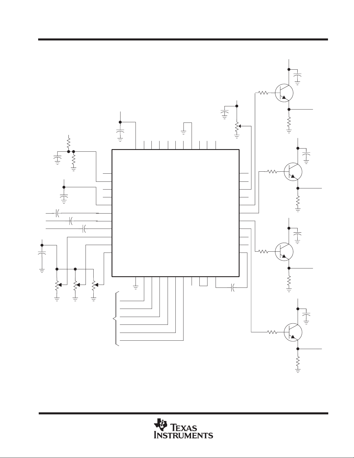
APPLICATION INFORMATION
C9
0.1 µF
43
42
41
40
39
38
37
36
35
34
ALC–
ALC+
RESET
ALCDRV
GND13SWR14SWG15SWB16PCL117PBL18PCL219HL20YSW21YAGCIN
GATE
TL1051
Video
Preprocessor
GATEIN
GATEOUT
GND
ALCREF
AGCSET
AGCCONT
WCPCONT
22
AGCDET
AGCOUT
AGCLMT
YCLAMP
YAGC
TL1051
VIDEO PREPROCESSOR CIRCUIT
SOCS032B – NOVEMBER 1991
5 V
C10
0.1 µF
Q1
2N3904
BOUT
R11
1 kΩ
5 V
C11
0.1 µF
Q2
2N3904
GOUT
R12
1 kΩ
5 V
C12
0.1 µF
Q3
2N390
4
ROUT
R13
1 kΩ
5 V
C13
0.1 µF
Q4
2N3904
YOUT
R6
10 kΩ
REF2V
BOUT
GOUT
ROUT
YOUT
YALC
0.1 µF
C8
5 V
33
32
31
30
29
28
27
26
25
24
23
R7
100 Ω
R8
100 Ω
R9
100 Ω
R10
100 Ω
R14
1 kΩ
NOTE A: This application circuit shows TTL signals originating from the TI SN28835 1/2-Inch NTSC Timer. However, the TL1051 video
preprocessor interfaces equally well with a TI TMS3471C 2/3-Inch NTSC timer, a TI SN28837 1/2-Inch PAL timer, or a user-defined
timing generator.
Figure 5. Typical Application Circuit
POST OFFICE BOX 655303 • DALLAS, TEXAS 75265
4-11
Page 12

TL1051
VIDEO PREPROCESSOR CIRCUIT
SOCS032B – NOVEMBER 1991
MECHANICAL DATA
FR/S-PDFP-G44 PLASTIC QUAD FLATPACK
33 23
34
44
2,25 MAX
22
12
111
8,00 TYP
10,20
SQ
9,80
12,80
SQ
12,00
0,80 TYP
0,40
0,20
0,10 MIN
Seating Plane
0,20
0,10
0°–10°
0,80
0,30
NOTES: A. All linear dimensions are in millimeters.
B. This drawing is subject to change without notice.
4-12
0,10
4040159/A–10/93
POST OFFICE BOX 655303 • DALLAS, TEXAS 75265
Page 13

IMPORTANT NOTICE
T exas Instruments and its subsidiaries (TI) reserve the right to make changes to their products or to discontinue
any product or service without notice, and advise customers to obtain the latest version of relevant information
to verify, before placing orders, that information being relied on is current and complete. All products are sold
subject to the terms and conditions of sale supplied at the time of order acknowledgement, including those
pertaining to warranty, patent infringement, and limitation of liability.
TI warrants performance of its semiconductor products to the specifications applicable at the time of sale in
accordance with TI’s standard warranty. Testing and other quality control techniques are utilized to the extent
TI deems necessary to support this warranty . Specific testing of all parameters of each device is not necessarily
performed, except those mandated by government requirements.
CERT AIN APPLICATIONS USING SEMICONDUCTOR PRODUCTS MAY INVOLVE POTENTIAL RISKS OF
DEATH, PERSONAL INJURY, OR SEVERE PROPERTY OR ENVIRONMENTAL DAMAGE (“CRITICAL
APPLICATIONS”). TI SEMICONDUCTOR PRODUCTS ARE NOT DESIGNED, AUTHORIZED, OR
WARRANTED TO BE SUITABLE FOR USE IN LIFE-SUPPORT DEVICES OR SYSTEMS OR OTHER
CRITICAL APPLICA TIONS. INCLUSION OF TI PRODUCTS IN SUCH APPLICATIONS IS UNDERST OOD TO
BE FULLY AT THE CUSTOMER’S RISK.
In order to minimize risks associated with the customer’s applications, adequate design and operating
safeguards must be provided by the customer to minimize inherent or procedural hazards.
TI assumes no liability for applications assistance or customer product design. TI does not warrant or represent
that any license, either express or implied, is granted under any patent right, copyright, mask work right, or other
intellectual property right of TI covering or relating to any combination, machine, or process in which such
semiconductor products or services might be or are used. TI’s publication of information regarding any third
party’s products or services does not constitute TI’s approval, warranty or endorsement thereof.
Copyright 1998, Texas Instruments Incorporated
 Loading...