

TL087, TL088, TL287, TL288
V
max
JFET-INPUT OPERATIONAL AMPLIFIERS
SLOS082A – D2484, MARCH 1979 – REVISED JANUARY 1993
• Low Input Offset Voltage . . . 0.5 mV Max
• Low Power Consumption
• Wide Common-Mode and Differential
Voltage Ranges
• Low Input Bias and Offset Currents
• High Input Impedance . . . JFET-Input Stage
• Internal Frequency Compensation
• Latch-Up-Free Operation
• High Slew Rate . . . 18 V/µs Typ
• Low T otal Harmonic Distortion
0.003% Typ
description
These JFET-input operational amplifiers incorporate well-matched high-voltage JFET and bipolar transistors
in a monolithic integrated circuit. They feature low input offset voltage, high slew rate, low input bias and offset
currents, and low temperature coefficient of input offset voltage. Offset-voltage adjustment is provided for the
TL087 and TL088.
The C-suffix devices are characterized for operation from 0°C to 70°C, and the I-suffix devices are characterized
for operation from –40°C to 85°C. The M-suffix devices are characterized for operation over the full military
temperature range of –55°C to 125°C.
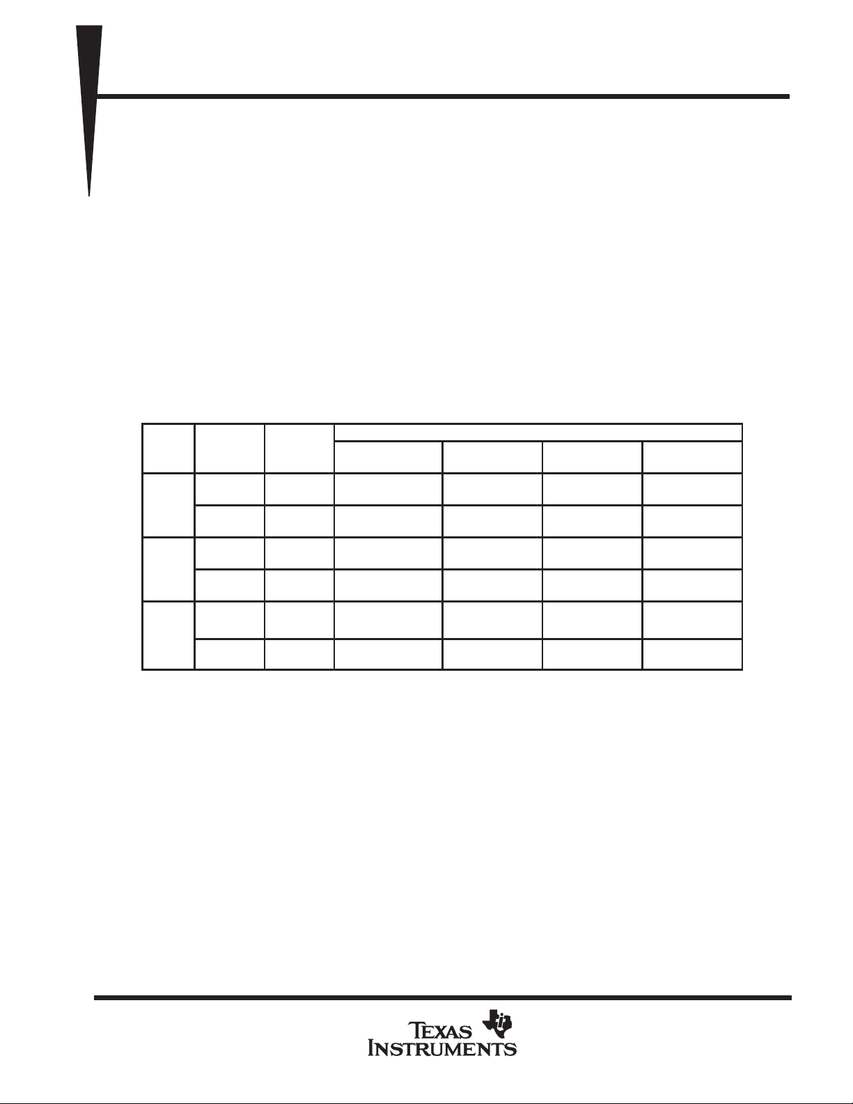
AVAILABLE OPTIONS
(JG)
PACKAGE
TL087CP
TL088CP
TL287CP
TL288CP
TL087IP
TL088IP
TL287IP
TL288IP
PLASTIC DIP
(P)
FLAT
(U)
T
A
0°C
to
70°C Dual
–40°C
to
85°C Dual
–55°C
to
125°C
TYPE
Single
Single
Single 1 mV TL088MJG TL088MU
Dual
IO
AT 25°C
0.5 mV
1 mV
0.5 mV
1 mV
0.5 mV
1 mV
0.5 mV
1 mV
1 mV TL288MJG TL288MU
SMALL OUTLINE
(D)
TL087CD
TL088CD
TL287CD
TL288CD
TL087ID
TL088ID
TL287ID
TL288ID
CERAMIC DIP
TL087CJG
TL088CJG
TL287CJG
TL288CJG
TL087IJG
TL088IJG
TL287IJG
TL288IJG
The D package is available taped and reeled. Add the suffix R to the device type (e.g., TL087CDR).
PRODUCTION DATA information is current as of publication date.
Products conform to specifications per the terms of Texas Instruments
standard warranty. Production processing does not necessarily include
testing of all parameters.
POST OFFICE BOX 655303 • DALLAS, TEXAS 75265
Copyright 1993, Texas Instruments Incorporated
1
TL087, TL088, TL287, TL288
JFET-INPUT OPERATIONAL AMPLIFIERS
SLOS082A – D2484, MARCH 1979 – REVISED JANUAR Y 1993
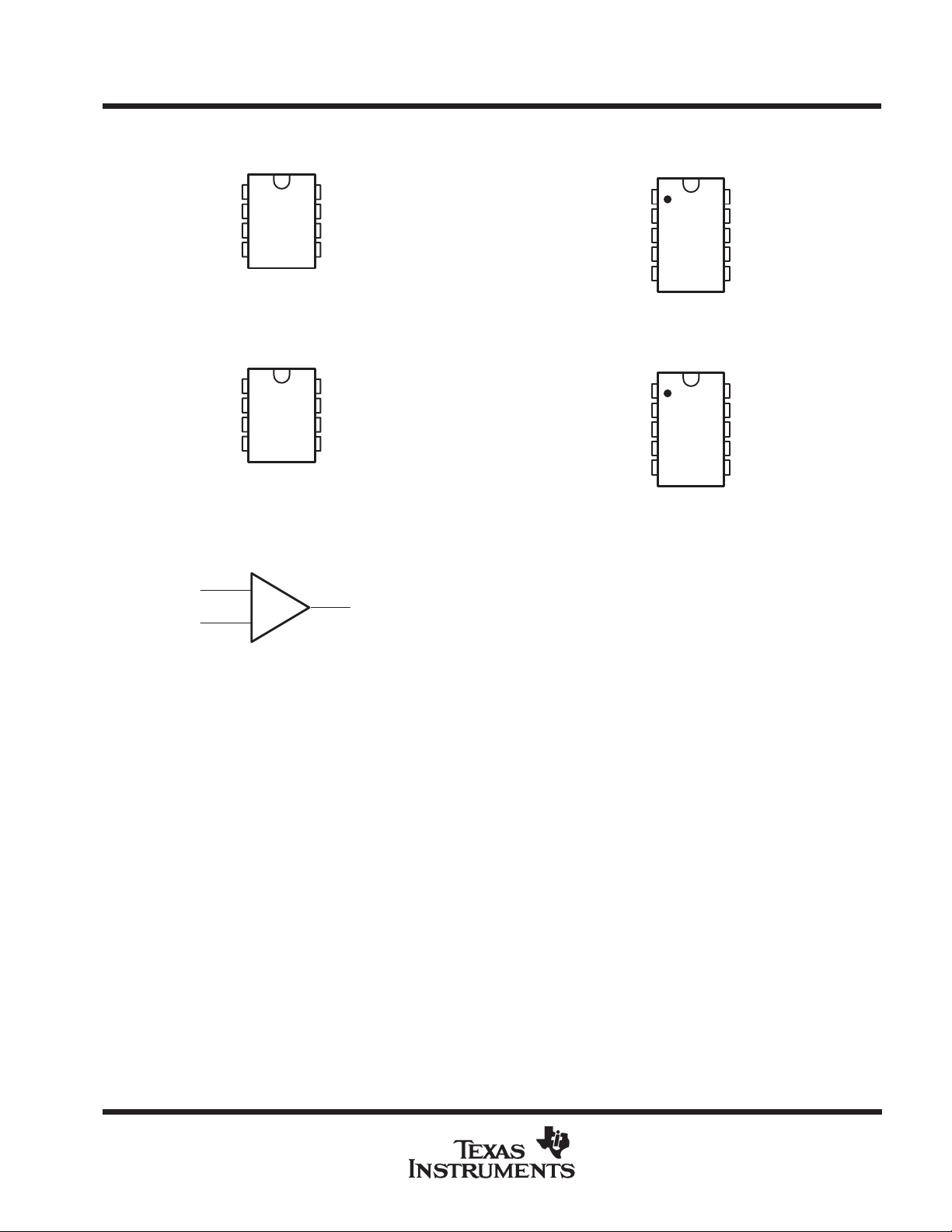
TL087, TL088
D, JG, OR P PACKAGE
(TOP VIEW)
OFFSET N1
IN –
V
CC –
1OUT
1IN –
1IN+
V
CC –
NC – No internal connection
1
2
IN+
3
4
TL287, TL288
D, JG, OR P PACKAGE
(TOP VIEW)
1
2
3
4
symbol (each amplifier)
NC
8
V
7
CC+
OUT
6
OFFSET N2
5
V
8
CC +
2OUT
7
2IN –
6
2IN+
5
NC
OFFSET N1
IN –
IN+
V
CC –
NC
1OUT
1IN –
1IN+
V
CC –
TL088M
U PACKAGE
(TOP VIEW)
1
10
2
3
4
5
U PACKAGE
(TOP VIEW)
1
2
3
4
5
9
8
7
6
TL288M
10
9
8
7
6
NC
NC
V
CC+
OUT
OFFSET N2
NC
V
CC +
2OUT
2IN –
2IN+
IN +
IN –
+
OUT
–
2
POST OFFICE BOX 655303 • DALLAS, TEXAS 75265
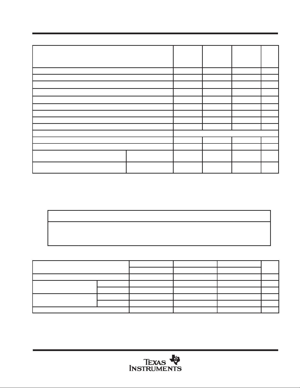
TL087, TL088, TL287, TL288
UNIT
Common-mode input voltage, V
Input voltage, V
JFET-INPUT OPERATIONAL AMPLIFIERS
SLOS082A – D2484, MARCH 1979 – REVISED JANUAR Y 1993
absolute maximum ratings over operating free-air temperature range (unless otherwise noted)
TL087I
TL088M
TL288M
Supply voltage, VCC+ (see Note 1) 18 18 18 V
Supply voltage, VCC– (see Note 1) –18 –18 –18 V
Differential input voltage (see Note 2)
Input voltage (see Notes 1 and 3)
Input current, II (each Input) ±1 ±1
Output current, IO (each output) ±80 ±80 ±80 mA
Total VCC+ terminal current 160 160 160 mA
Total VCC– terminal current –160 –160 –160 mA
Duration of output short circuit (see Note 4) unlimited unlimited unlimited
Continuous total dissipation See Dissipation Rating Table
Operating free-air temperature range –55 to 125 –25 to 85 0 to 70 °C
Storage temperature range –65 to 150 –65 to 150 –65 to 150 °C
Lead temperature 1,6 mm (1/16 inch) from
case for 60 seconds
Lead temperature 1,6 mm (1/16 inch) from
case for 10 seconds
NOTES: 1. All voltage values, except differential voltages, are with respect to the midpoint between V
2. Differential voltages are at the noninverting input terminal with respect to the inverting input terminal.
3. The magnitude of the input voltage must never exceed the magnitude of the supply voltage or 15 V, whichever is less.
4. The output may be shorted to ground or to either supply. Temperature and/or supply voltages must be limited to ensure that the
dissipation rating is not exceeded.
JG or U package 300 300 300 °C
D or P package 260 260 °C
±30 ±30 ±30
±15 ±15 ±15
TL088I
TL287I
TL288I
CC+
and V
CC–
TL087C
TL088C
TL287C
TL288C
±1 mA
.
UNIT
V
V
PACKAGE
D 725 mW 5.8 mW/°C 464 mW 377 mW N/A
JG 1050 mW 8.4 mW/°C 672 mW 546 mW 210 mW
P 1000 mW 8.0 mW/°C 640 mW 520 mW N/A
U 675 mW 5.4 mW/°C 432 mW 351 mW 135 mW
TA ≤ 25°C
POWER RATING
DERATING FACTOR
recommended operating conditions
Supply voltage, V
p
Operating free-air temperature, T
CC
V
= ±5 V –1 4 –1 4 –1 4 V
p
I
CC±
IC
V
= ±15 V –11 11 –11 11 –11 11 V
CC±
V
= ±5 V –1 4 –1 4 –1 4 V
CC±
V
= ±15 V –11 11 –11 11 –11 11 V
CC±
A
DISSIPATION RATING TABLE
TA = 70°C
ABOVE TA = 25°C
C-SUFFIX I-SUFFIX M-SUFFIX
MIN NOM MAX MIN NOM MAX MIN NOM MAX
±5 ±5 ±5 ±5 ±5 ±15 V
0 70 –40 85 –55 125 °C
POWER RATING
TA = 85°C
POWER RATING
TA = 125°C
POWER RATING
POST OFFICE BOX 655303 • DALLAS, TEXAS 75265
3
4
TL088, TL288
0.130.110.1
1
VIOI
V
TL088, TL288
632.5
α
R
T
25°C to MAX
1088µV/°C
IIOInput offset current
C
t
voltage range
Maxi
k
()
out ut voltage swing
T
range
50
1055010550105
A
V/mV
252525
CMRR
j
809380938093dB
S
ratio (∆V
CC±
/∆VIO)
I
CC
y
26
2.8
2.6
2.8
2.6
2.8
mA
POST OFFICE BOX 1443 HOUSTON, TEXAS 77001
POST OFFICE BOX 655303 DALLAS, TEXAS 75265
•
•
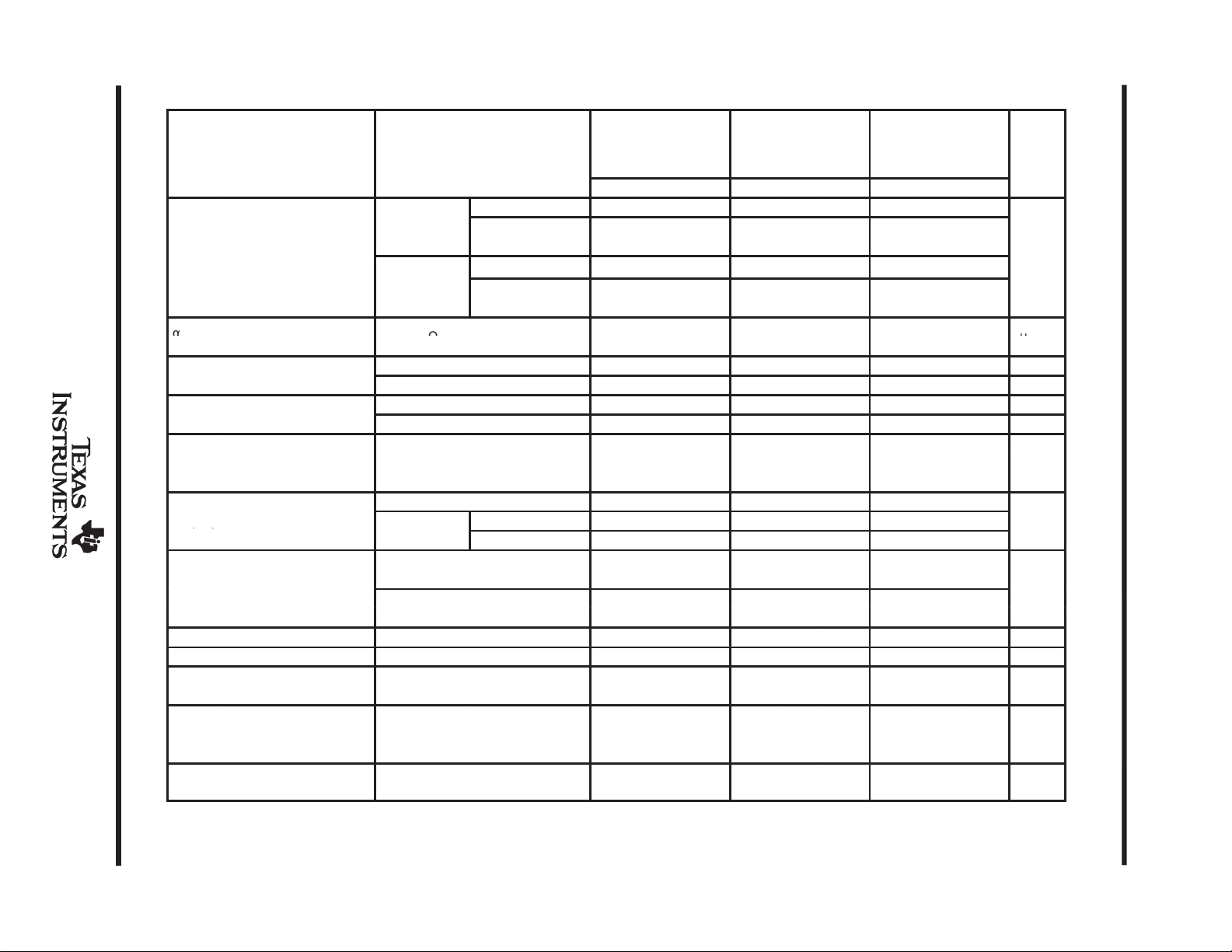
electrical characteristics, V
PARAMETER TEST CONDITIONS
nput offset voltage
VIO
I
IB
V
ICR
V
O(PP)
VD
B
1
r
i
k
SVR
†
All characteristics are measured under open–loop conditions with zero common-mode input voltage unless otherwise specified. Full range for TA is –55°C to 125°C for TL_88M;
–40°C to 85°C for TL_8_I; and 0°C to 70°C for TL_8_C.
‡
Input bias currents of a FET-input operational amplifier are normal junction reverse currents, which are temperature sensitive. Pulse techniques must be used that will maintain
the junction temperature as close to the ambient temperature as possible.
Temperature coefficient
of input offset voltage
p
Input bias current
ommon-mode inpu
mum-peak-to-pea
p
Large-signal differential TA = 25°C
voltage amplification RL ≥ 2 kΩ, VO = ±10 V,
Unity-gain bandwidth TA = 25°C 3 3 3 MHz
Input resistance TA = 25°C 10
Common–mode rejection
ratio
upply voltage rejection
Supply current
(per amplifier)
‡
= ±15 V
±
CC
TL087I
†
RS = 50 Ω, TL087, TL287 0.1 0.5 0.1 0.5
VO = 0
TA = 25°C
RS = 50 Ω,
VO = 0,
TA = full range
= 50 Ω,
S
TA = 25°C 5 5 100 5 100 pA
TA = full range 25 3 2 nA
TA = 25°C 30 30 200 30 200 pA
TA = full range 100 20 7 nA
TA = 25°C
TA = 25°C, RL = 10 kΩ 24 27 24 27 24 27
= full
A
RL ≥ 2 kΩ, VO = ±10 V,
TA = full range
RS = 50 Ω, VO = 0 V,
VIC = V
ICR
RS = 50 Ω, VO = 0 V,
V
= ±9 V to ±15 V, 80 99 80 99 80 99 dB
CC±
TA = 25°C
No load, VO = 0 V,
TA = 25°C
TL087, TL287 2 1.5
°
=
A
RL ≥ 10 kΩ 24 24 24 V
RL ≥ 2 kΩ 20 20 20
min, TA = 25°C
TL088M
TL288M
MIN TYP MAX MIN TYP MAX MIN TYP MAX
V
+ 4 V
CC–
to to to
V
–4 V
CC+
12
TL088I
TL287I
TL288I
+4 V
CC–
–4 V
CC+
12
10
CC–
CC+
TL087C
TL088C
TL287C
TL288C
+4
–4
10
UNIT
m
12
°
V
Ω
TL087, TL088, TL287, TL288
JFET-INPUT OPERATIONAL AMPLIFIERS
SLOS082A – D2484, MARCH 1979 – REVISED JANUARY 1993
operating characteristics VCC = ±15 V, TA = 25°C
PARAMETER TEST CONDITIONS
SR Slew rate at unity gain
t
Rise time VI = 20 mV, RL = 2 kΩ, 55 55 ns
r
Overshoot factor CL = 100 pF, AVD = 1 25% 25%
V
Equivalent input noise voltage RS = 100 Ω, f = 1 kHz 19 19
n
VI = 10 V,
CL = 100 pF,
RL = 2 kΩ,
AVD = 1
PARAMETER MEASUREMENT INFORMATION
V
CC+
–
+
V
I
V
CC–
C
L
(see Note A)
NOTE A: CL includes fixture capacitance.
V
O
R
L
TL087, TL088, TL287, TL288
JFET-INPUT OPERATIONAL AMPLIFIERS
SLOS082A – D2484, MARCH 1979 – REVISED JANUARY 1993
TL088M, TL288M
MIN TYP MAX MIN TYP MAX
18 8 18 V/µs
Overshoot
90%
10%
tr – Rise Time
TL087I, TL087C
TL088I, TL088C
UNIT
nV/√Hz
Figure 1. Slew Rate, Rise/Fall Time, Figure 2. Rise Time and Overshoot
and Overshoot Test Circuit Waveform
10 kΩ
V
10 kΩ
V
CC+
–
+
V
R
S
R
CC–
S
V
O
V
I
100
NOTE A: CL includes fixture capacitance.
CC+
–
+
V
CC–
C
(see Note A)
V
O
L
R
L
Figure 3. Noise Voltage Test Circuit Figure 4. Unity-Gain Brandwidth and
Phase Margin Test Circuit
V
Ground Shield
pA
pA
CC+
–
+
V
CC–
Figure 5. Input Bias and Offset
Current Test Circuit
POST OFFICE BOX 655303 • DALLAS, TEXAS 75265
5

TL087, TL088, TL287, TL288
JFET-INPUT OPERATIONAL AMPLIFIERS
SLOS082A – D2484, MARCH 1979 – REVISED JANUAR Y 1993
typical values
Typical values as presented in this data sheet represent the median (50% point) of device parametric
performance.
input bias and offset current
At the picoamp bias current level typical of these JFET operational amplifiers, accurate measurement of the bias
current becomes difficult. Not only does this measurement require a picoammeter , but test socket leakages can
easily exceed the actual device bias currents. To accurately measure these small currents, T exas Instruments
uses a two-step process. The socket leakage is measured using picoammeters with bias voltages applied, but
with no device in the socket. The device is then inserted in the socket and a second test that measures both
the socket leakage and the device input bias current is performed. The two measurements are then subtracted
algebraically to determine the bias current of the device.
6
POST OFFICE BOX 655303 • DALLAS, TEXAS 75265

table of graphs
α
I
V
V
A
CMRR Common-mode rejection ratio
k
SVR
I
I
SR Slew rate
THD T otal harmonic distortion vs Frequency 35
φ
TL087, TL088, TL287, TL288
JFET-INPUT OPERATIONAL AMPLIFIERS
SLOS082A – D2484, MARCH 1979 – REVISED JANUARY 1993
TYPICAL CHARACTERISTICS
Temperature coefficient of input offset voltage Distribution 6, 7
VIO
Input offset current vs Temperature 8
IO
vs V
I
Input bias current
IB
V
Common-mode input voltage range limits
I
Differential input voltage vs Output voltage 12
ID
Maximum peak output voltage swing
OM
Differential voltage amplification
VD
z
Output impedance vs Frequency 24
o
Supply-voltage rejection ratio vs Temperature 25
Short-circuit output current
OS
Supply current
CC
Overshoot factor vs C
V
Equivalent input noise voltage vs Frequency 34
n
B
Unity-gain bandwidth
1
Phase margin
m
Phase shift vs Frequency 20
Pulse response
IC
vs Temperature
vs V
CC
vs Temperature
vs V
CC
vs Output current
vs Frequency
vs Temperature
vs R
L
vs Frequency
vs Temperature
vs Frequency
vs Temperature
vs V
CC
vs Time
vs Temperature
vs V
CC
vs Temperature
vs R
L
vs Temperature
L
vs V
CC
vs Temperature
vs V
CC
vs C
L
vs Temperature
Small-signal
Large-signal
FIGURE
9
8
10
11
13
17
14, 15, 16
18
19
20
21
22
23
26
27
28
29
30
31
32
33
36
37
38
39
40
41
42
POST OFFICE BOX 655303 • DALLAS, TEXAS 75265
7

TL087, TL088, TL287, TL288
JFET-INPUT OPERATIONAL AMPLIFIERS
SLOS082A – D2484, MARCH 1979 – REVISED JANUAR Y 1993
DISTRIBUTION OF TL088
INPUT OFFSET VOLTAGE
TEMPERATURE COEFFICIENT
20
120 Units Tested From 2 Wafer Lots
V
= ±15 V
CC±
TA = 25°C to 125°C
16
P Package
12
8
Percentage of Units – %
4
0
–25
–20 –15 –10 –5 0 5 10 15 20
α
– Temperature Coefficient – µV/°C
VIO
TYPICAL CHARACTERISTICS
20
172 Amplifiers Tested From 2 Wafer Lots
V
CC±
TA = 25°C to 125°C
P Package
15
One unit at – 34.6 µV/°C
10
Percentage of Amplifiers – %
5
0
25
–30
†
DISTRIBUTION OF TL288
INPUT OFFSET VOLTAGE
TEMPERATURE COEFFICIENT
= ±15 V
–20 –10 0 10 20
α
– Temperature Coefficient – µV/°C
VIO
30
Figure 6 Figure 7
INPUT BIAS CURRENT AND
INPUT OFFSET CURRENT
vs
FREE-AIR TEMPERATURE
100
10
0.1
IO
I
0.01
IB
IIB and IIO – Bias and Offset Currents – nA
I
0.001
V
= ±15 V
CC±
VO = 0
VIC = 0
I
IB
1
I
IO
25
45 65 85 105 125
TA – Free-Air Temperature – °C
INPUT BIAS CURRENT
COMMON-MODE INPUT VOLTAGE
10
V
= ±15 V
CC±
TA = 25°C
5
0
IB
–5
I
IIB – Input Bias Current – nA
–10
–15
–10 –5 0 5 10
VIC – Common-Mode Input Voltage – V
vs
15
Figure 8 Figure 9
†
Data at high and low temperatures are applicable within the rated operating free-air temperature ranges of the various devices.
8
POST OFFICE BOX 655303 • DALLAS, TEXAS 75265

TL087, TL088, TL287, TL288
JFET-INPUT OPERATIONAL AMPLIFIERS
SLOS082A – D2484, MARCH 1979 – REVISED JANUARY 1993
16
12
8
4
0
–4
–8
IC
V
VIC – Common-Mode Input Voltqge – V
–12
–16
0
TYPICAL CHARACTERISTICS
COMMON-MODE
INPUT VOLTAGE RANGE LIMITS
vs
SUPPLY VOLTAGE
Positive Limit
Negative Limit
2 4 6 8 10 12 14 16
|V
| – Supply Voltage – V
CC±
20
15
10
5
0
–5
–10
IC
V
VIC – Common-Mode Input Voltqge – V
–15
–20
–75
†
COMMON-MODE
INPUT VOLTAGE RANGE LIMITS
vs
FREE-AIR TEMPERATURE
V
= ±15 VTA = 25°C
CC±
Positive Limit
Negative Limit
–50 –25 0 25 50 75 100 125
TA – Free-Air Temperature – °C
V
VO – Output Voltage – V
O
15
10
–5
–10
–15
–400
Figure 10 Figure 11
OUTPUT VOLTAGE
vs
DIFFERENTIAL INPUT VOLTAGE
16
V
= ±15 V
CC±
TA = 25°C
5
0
RL = 600 Ω
RL = 1 kΩ
RL = 2 kΩ
RL = 10 kΩ
–200 0 200 400
VID – Differential Input Voltage – µV
12
8
4
0
–4
–8
OM
–12
V
VOM – Maximum Peak Output Voltage – V
–16
MAXIMUM PEAK OUTPUT VOLTAGE
vs
SUPPLY VOLTAGE
TA = 25°C
RL = 10 kΩ
RL = 10 kΩ
0
2 4 6 8 10 12 14 16
|V
| – Supply Voltage – V
CC±
V
OM+
RL = 2 kΩ
RL = 2 kΩ
V
OM –
Figure 12 Figure 13
†
Data at high and low temperatures are applicable within the rated operating free-air temperature ranges of the various devices.
POST OFFICE BOX 655303 • DALLAS, TEXAS 75265
9

TL087, TL088, TL287, TL288
JFET-INPUT OPERATIONAL AMPLIFIERS
SLOS082A – D2484, MARCH 1979 – REVISED JANUAR Y 1993
TYPICAL CHARACTERISTICS
MAXIMUM PEAK-TO-PEAK OUTPUT VOLTAGE
vs
FREQUENCY
30
V
= ±15 V
25
20
15
10
5
O(PP)
VOPP – Maximum Peak-to-Peak Output V oltage – V
0
V
10 k
CC±
TA = 125°C
V
= ±5 V
CC±
TA = –55°C
100 k 1 M 10 M
f – Frequency – Hz
Figure 14 Figure 15
RL = 2 kΩ
†
MAXIMUM PEAK-TO-PEAK OUTPUT VOLTAGE
vs
FREQUENCY
30
V
= ±15 V
CC±
25
20
15
10
O(PP)
VOPP – Maximum Peak-to-Peak Output V oltage – V
V
5
0
10 k
V
CC±
= ±5 V
100 k 1 M 10 M
f – Frequency – Hz
RL = 2 kΩ
TA = 25°C
MAXIMUM PEAK-TO-PEAK OUTPUT VOLTAGE
vs
FREQUENCY
30
25
V
= ±15 V
CC±
20
15
10
V
= ±5 V
5
O(PP)
VOPP – Maximum Peak-to-Peak Output V oltage – V
V
0
10 k 100 k
CC±
1 M 10 M
f – Frequency – Hz
Figure 16 Figure 17
RL = 10 kΩ
TA = 25°C
16
14
12
10
8
6
4
OM
2
V
VOM – Maximum Peak Output Voltage – V
0
0
MAXIMUM PEAK OUTPUT VOLTAGE
vs
OUTPUT CURRENT
V
= ±15 V
CC±
TA = 25°C
V
OM+
V
OM–
10 20 30 40
515253545
|IO| – Output Current – mA
50
†
Data at high and low temperatures are applicable within the rated operating free-air temperature ranges of the various devices.
10
POST OFFICE BOX 655303 • DALLAS, TEXAS 75265

TL087, TL088, TL287, TL288
JFET-INPUT OPERATIONAL AMPLIFIERS
SLOS082A – D2484, MARCH 1979 – REVISED JANUARY 1993
16
12
8
4
0
–4
–8
OM
V
VOM – Maximum Peak Output Voltage – V
–12
–16
–75
TYPICAL CHARACTERISTICS
MAXIMUM PEAK OUTPUT VOLTAGE
vs
FREE-AIR TEMPERATURE
RL = 10 kΩ
V
OM+
V
OM–
–50 –25 0 25 50 75 100
TA – Free-Air Temperature – °C
RL = 2 kΩ
RL = 2 kΩ
RL = 10 kΩ
V
CC±
= ±15 V
125
†
LARGE-SIGNAL VOLTAGE AMPLIFICATION
vs
LOAD RESISTANCE
250
VO = ±1 V
TA = 25°C
200
V
150
V
100
50
VD
AVD – Differential Voltage Amplification – V/m V
A
0
0.4
1 4 10 40
RL – Load Resistance – kΩ
CC±
CC±
= ±15 V
= ±5 V
100
LARGE-SIGNAL DIFFERENTIAL VOLTAGE
6
10
5
10
4
10
3
10
2
10
1
10
VD
1
AVD – Differential Voltage Amplification
A
0.1
10
Figure 18 Figure 19
AMPLIFICATION AND PHASE SHIFT
vs
FREQUENCY
V
= ±15 V
CC±
RL = 2 kΩ
CL = 25 pF
TA = 25°C
A
VD
Phase Shift
100 1 k 10 k 100 k 1 M
f – Frequency – Hz
10 M
0°
30°
60°
90°
120°
150°
180°
1000
400
100
Phase Shift
40
VD
AVD – Differential Voltage Amplification – V/mV
A
10
LARGE-SIGNAL VOLTAGE AMPLIFICATION
vs
FREE-AIR TEMPERATURE
V
= ±15 V
CC±
VO = ±10 V
RL = 10 kΩ
RL = 2 kΩ
–75
–50 –25 0 25 50 75 100
TA – Free-Air Temperature – °C
125
Figure 20 Figure 21
†
Data at high and low temperatures are applicable within the rated operating free-air temperature ranges of the various devices.
POST OFFICE BOX 655303 • DALLAS, TEXAS 75265
11

TL087, TL088, TL287, TL288
ООООООО
JFET-INPUT OPERATIONAL AMPLIFIERS
SLOS082A – D2484, MARCH 1979 – REVISED JANUAR Y 1993
TYPICAL CHARACTERISTICS
COMMON-MODE REJECTION RATIO
vs
FREQUENCY
100
V
90
80
70
60
50
40
30
20
10
CMRR – Common-Mode Rejection Ratio – dB
0
10
f – Frequency – Hz
CC±
TA = 25°C
= ±15 V
1 M100 k10 k1 k100 10 M
†
COMMON-MODE REJECTION RATIO
vs
FREE-AIR TEMPERATURE
100
VIC = V
95
90
85
80
75
CMRR – Common-Mode Rejection Ratio – dB
70
–75
–50 – 25 0 25 50 75 100
min
ICR
V
= ±15 V
CC±
V
= ±5 V
CC±
TA – Free-Air Temperature – °C
125
Figure 22 Figure 23
OUTPUT IMPEDANCE
100
AVD = 100
Ω
10
AVD = 10
1
o
z0 – Output Inppedance –
z
0.1
1 k
AVD = 1
10 k 100 k
f – Frequency – Hz
vs
FREQUENCY
V
= ±15 V
CC±
TA = 25°C
ro (open loop) ≈ 250 Ω
1 M
SUPPLY-VOLTAGE REJECTION RATIO
FREE-AIR TEMPERATURE
110
V
= ±5 V to ±15 V
CC±
106
102
98
94
SVR
k
kSVR – Supply-Voltage Rejection Ratio – dB
90
–75
–50 –25 0 25 50 75 100
TA – Free-Air Temperature – °C
vs
125
†
Data at high and low temperatures are applicable within the rated operating free-air temperature ranges of the various devices.
12
Figure 24 Figure 25
POST OFFICE BOX 655303 • DALLAS, TEXAS 75265

TL087, TL088, TL287, TL288
JFET-INPUT OPERATIONAL AMPLIFIERS
SLOS082A – D2484, MARCH 1979 – REVISED JANUARY 1993
SHORT-CIRCUIT OUTPUT CURRENT
vs
SUPPLY VOLTAGE
60
VO = 0
0
TA = 25°C
VID = – 1 V
0
2 4 6 8 10 12 14
|V
| – Supply Voltage – V
CC±
VID = 1 V
40
20
–20
–40
OS
IOS – Short-Circuit Output Current – mA
I
–60
TYPICAL CHARACTERISTICS
SHORT-CIRCUIT OUTPUT CURRENT
60
40
20
0
–20
–40
OS
IOS – Short-Circuit Output Current – mA
I
16
–60
†
VID = –1 V
vs
TIME
VID = 1 V
Time – Seconds
V
= ±15 V
CC±
TA = 25°C
6050403020100
Figure 26 Figure 27
SHORT-CIRCUIT OUTPUT CURRENT
vs
FREE-AIR TEMPERATURE
60
V
= ±15 V
V
V
V
CC±
CC±
CC±
CC±
= ±5 V
= ±5 V
= ±15 V
1007550250–25–50 125–75
VID = 1 V
40
20
VID = 1 V
0
–20
–40
OS
IOS – Short-Circuit Output Current – mA
I
–60
VID = –1 V
VID = –1 V
VO = 0
TA – Free-Air Temperature – °C
Figure 28
†
Data at high and low temperatures are applicable within the rated operating free-air temperature ranges of the various devices.
POST OFFICE BOX 655303 • DALLAS, TEXAS 75265
13

TL087, TL088, TL287, TL288
JFET-INPUT OPERATIONAL AMPLIFIERS
SLOS082A – D2484, MARCH 1979 – REVISED JANUAR Y 1993
SUPPLY CURRENT
SUPPLY VOLTAGE
3
2.5
2
1.5
1
CC
ICC – Supply Current – mA
I
0.5
0
0
2 4 6 8 10 12 14
|V
CC±
TYPICAL CHARACTERISTICS
vs
TA = 25°C
TA = –55°C
TA = 125°C
| – Supply Voltage – V
VO = 0
No Load
16
†
SUPPLY CURRENT
FREE-AIR TEMPERATURE
3
2.5
2
1.5
1
CC
ICC – Supply Current – mA
I
0.5
0
–50 –25 0 25 50 75 100
–75
TA – Free-Air Temperature – °C
vs
V
V
CC±
CC±
= ±15 V
= ±5 V
VO = 0
No Load
125
30
25
sµ
20
15
10
SR – Slew Rate – V/s
5
0
0.4
1 4 10 40 100
RL – Load Resistance – kΩ
Figure 29 Figure 30
SLEW RATE
vs
LOAD RESISTANCE
SR+
SR–
V
CL = 100 pF
TA = 25°C
= ±15 V
CC±
See Figure 1
30
25
sµ
20
15
10
SR – Slew Rate – V/s
5
0
–75
–50 –25 0 25 50 75 100
TA – Free-Air Temperature – °C
SLEW RATE
vs
FREE-AIR TEMPERATURE
SR+
SR–
V
= ±15 V
CC±
RL = 2 kΩ
CL = 100 pF
See Figure 1
125
Figure 31 Figure 32
†
Data at high and low temperatures are applicable within the rated operating free-air temperature ranges of the various devices.
14
POST OFFICE BOX 655303 • DALLAS, TEXAS 75265

TL087, TL088, TL287, TL288
JFET-INPUT OPERATIONAL AMPLIFIERS
SLOS082A – D2484, MARCH 1979 – REVISED JANUARY 1993
OVERSHOOT FACTOR
50
40
30
20
Overshoot Factor – %
10
0
0
50 100 150 200 250
CL – Load Capacitance – pF
TYPICAL CHARACTERISTICS
†
EQUIVALENT INPUT NOISE VOLTAGE
vs
LOAD CAPACITANCE
V
= ±5 V
CC±
V
CC±
V
I(PP)
RL = 2 kΩ
TA = 25°C
See Figure 1
= ±15 V
= ±10 mV
300
100
70
nV/ Hz
50
40
30
20
n
Vn – Equivalent Input Noise Voltage – nV/Hz
V
10
10
FREQUENCY
100 1 k 10 k 100 k
f – Frequency – Hz
Figure 33 Figure 34
vs
V
= ±15 V
CC±
RS = 100 Ω
TA = 25°C
See Figure 3
TOTAL HARMONIC DISTORTION
FREQUENCY
1
V
= ±15 V
CC±
AVD = 1
V
) = 6 V
O(rms
TA = 25°C
0.1
0.01
THD – Total Harmonic Distortion – %
0.001
100
1 k 10 k 100 k
f – Frequency – Hz
Figure 35 Figure 36
vs
UNITY-GAIN BANDWIDTH
vs
SUPPLY VOLTAGE
3.2
3.1
3
2.9
1
B
B1 – Unity-Gain Bandwidth – MHz
2.8
2.7
0
2 4 6 8 10 12 14
|V
| – Supply Voltage – V
CC±
VI = 10 mV
RL = 2 kΩ
CL = 25 pF
TA = 25°C
See Figure 4
16
†
Data at high and low temperatures are applicable within the rated operating free-air temperature ranges of the various devices.
POST OFFICE BOX 655303 • DALLAS, TEXAS 75265
15

TL087, TL088, TL287, TL288
JFET-INPUT OPERATIONAL AMPLIFIERS
SLOS082A – D2484, MARCH 1979 – REVISED JANUAR Y 1993
UNITY-GAIN BANDWIDTH
vs
FREE-AIR TEMPERATURE
4
V
3
V
CC±
2
VI = 10 mV
RL = 2 kΩ
1
1
B
B1 – Unity-Gain Bandwidth – MHz
CL = 25 pF
See Figure 4
0
–75
–50 –25 0 25 50 75 100
TA – Free-Air Temperature – °C
CC±
TYPICAL CHARACTERISTICS
= ±15 V
= ±5 V
m
m – Phase Margin
φ
125
65°
63°
61°
59°
57°
55°
†
PHASE MARGIN
vs
SUPPLY VOLTAGE
2 4 6 8 10 12 14
0
|V
| – Supply Voltage – V
CC±
VI = 10 mV
RL = 2 kΩ
CL = 25 pF
TA = 25°C
See Figure 4
16
70°
65°
60°
55°
m
m – Phase Margin
50°
φ
45°
40°
0
10 20
Figure 37 Figure 38
PHASE MARGIN
vs
LOAD CAPACITANCE
VI = 10 mV
RL = 2 kΩ
TA = 25°C
See Figure 4
V
= ±15 V
CC±
V
= ±5 V
CC±
30 40 50 60 70 80 90
CL – Load Capacitance – pF
100
65°
63°
61°
59°
m
m – Phase Margin
φ
57°
55°
–50 –25 0 25 50 75 100
–75
PHASE MARGIN
FREE-AIR TEMPERATURE
TA – Free-Air Temperature – °C
vs
V
CC±
V
CC±
= ±15 V
= ±5 V
VI = 10 mV
RL = 2 kΩ
CL = 25 pF
See Figure 4
125
Figure 39 Figure 40
†
Data at high and low temperatures are applicable within the rated operating free-air temperature ranges of the various devices.
16
POST OFFICE BOX 655303 • DALLAS, TEXAS 75265

JFET-INPUT OPERATIONAL AMPLIFIERS
SLOS082A – D2484, MARCH 1979 – REVISED JANUARY 1993
TYPICAL CHARACTERISTICS
TL087, TL088, TL287, TL288
O
V
VO – Output Voltage – mV
–12
–16
16
12
–4
–8
VOLTAGE-FOLLOWER
SMALL-SIGNAL
PULSE RESPONSE
8
6
O
V
VO – Output Voltage – mV
4
2
0
–2
–4
–6
–8
8
4
0
0 0.2 0.4 0.6 0.8 1.0
V
= ±15 V
CC±
RL = 2 kΩ
CL = 100 pF
TA = 25°C
See Figure 1
t – Time – µs
1.2
VOLTAGE-FOLLOWER
LARGE-SIGNAL
PULSE RESPONSE
V
= ±15 V
CC±
RL = 2 kΩ
CL = 100 pF
TA = 25°C
See Figure 1
0 1 2 3 4 5
t – Time – µs
6
Figure 41 Figure 42
POST OFFICE BOX 655303 • DALLAS, TEXAS 75265
17

TL087, TL088, TL287, TL288
JFET-INPUT OPERATIONAL AMPLIFIERS
SLOS082A – D2484, MARCH 1979 – REVISED JANUAR Y 1993
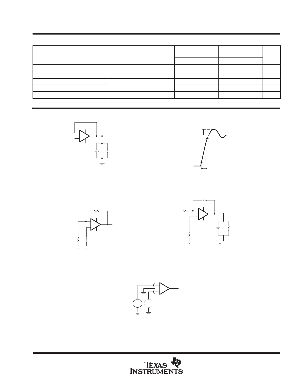
TYPICAL APPLICATION DATA
output characteristics
All operating characteristics are specified with 100-pF load capacitance. These amplifiers will drive higher
capacitive loads; however, as the load capacitance increases, the resulting response pole occurs at lower
frequencies, thereby causing ringing, peaking, or even oscillation. The value of the load capacitance at which
oscillation occurs varies with production lots. If an application appears to be sensitive to oscillation due to load
capacitance, adding a small resistance in series with the load should alleviate the problem. Capacitive loads
of 1000 pF and larger may be driven if enough resistance is added in series with the output (see Figure 43).
(a) CL = 100 pF, R = 0 (b) CL = 300 pF, R = 0 (c) CL = 350 pF, R = 0
(d) CL = 1000 pF, R = 0 (e) CL = 1000 pF, R = 50 Ω (f) CL = 1000 pF, R = 2 kΩ
Figure 43. Effect of Capacitive Loads
15 V
5 V
–5 V
–
+
–15 V
(see Note A)
R
C
L
V
2 kΩ
O
18
NOTE A: CL includes fixture capacitance
Figure 44. Test Circuit for Output Characteristics
POST OFFICE BOX 655303 • DALLAS, TEXAS 75265

TL087, TL088, TL287, TL288
JFET-INPUT OPERATIONAL AMPLIFIERS
SLOS082A – D2484, MARCH 1979 – REVISED JANUARY 1993
TYPICAL APPLICATION DATA
input characteristics
These amplifiers are specified with a minimum and a maximum input voltage that, if exceeded at either input,
could cause the device to malfunction.
Because of the extremely high input impedance and resulting low bias current requirements, these amplifiers
are well suited for low-level signal processing; however, leakage currents on printed circuit boards and sockets
can easily exceed bias current requirements and cause degradation in system performance. It is good practice
to include guard rings around inputs (see Figure 45). These guards should be driven from a low-impedance
source at the same voltage level as the common-mode input.
V
I
(a) NONINVERTING AMPLIFIER (b) INVERTING AMPLIFIER (c) UNITY–GAIN AMPLIFIER
+
V
–
O
V
I
–
V
+
O
V
I
–
+
Figure 45. Use of Guard Rings
noise performance
The noise specifications in op amp circuits are greatly dependent on the current in the first-stage diflferential
amplifier. The low input bias current requirments of these amplifiers result in a very low current noise. This
feature makes the devices especially favorable over bipolar devices when using values of circuit impedance
greater than 50 kΩ.
V
O
POST OFFICE BOX 655303 • DALLAS, TEXAS 75265
19

IMPORTANT NOTICE
T exas Instruments (TI) reserves the right to make changes to its products or to discontinue any semiconductor
product or service without notice, and advises its customers to obtain the latest version of relevant information
to verify, before placing orders, that the information being relied on is current and complete.
TI warrants performance of its semiconductor products and related software to the specifications applicable at
the time of sale in accordance with TI’s standard warranty. Testing and other quality control techniques are
utilized to the extent TI deems necessary to support this warranty. Specific testing of all parameters of each
device is not necessarily performed, except those mandated by government requirements.
Certain applications using semiconductor products may involve potential risks of death, personal injury, or
severe property or environmental damage (“Critical Applications”).
TI SEMICONDUCTOR PRODUCTS ARE NOT DESIGNED, INTENDED, AUTHORIZED, OR WARRANTED
TO BE SUITABLE FOR USE IN LIFE-SUPPORT APPLICATIONS, DEVICES OR SYSTEMS OR OTHER
CRITICAL APPLICATIONS.
Inclusion of TI products in such applications is understood to be fully at the risk of the customer. Use of TI
products in such applications requires the written approval of an appropriate TI officer . Questions concerning
potential risk applications should be directed to TI through a local SC sales office.
In order to minimize risks associated with the customer’s applications, adequate design and operating
safeguards should be provided by the customer to minimize inherent or procedural hazards.
TI assumes no liability for applications assistance, customer product design, software performance, or
infringement of patents or services described herein. Nor does TI warrant or represent that any license, either
express or implied, is granted under any patent right, copyright, mask work right, or other intellectual property
right of TI covering or relating to any combination, machine, or process in which such semiconductor products
or services might be or are used.
Copyright 1998, Texas Instruments Incorporated
 Loading...