

TIBPAL22V10-10C
HIGH-PERFORMANCE IMPACT-X PROGRAMMABLE ARRAY LOGIC CIRCUITS
SRPS015 – D3972, FEBRUARY 1992
• Second-Generation PLD Architecture
• High-Performance Operation:
f
(External Feedback) . . . 71 MHz
max
Propagation Delay . . . 10 ns Max
• Increased Logic Power – Up to 22 Inputs
and 10 Outputs
• Increased Product Terms – Average of 12
Per Output
• Variable Product Term Distribution
Allows More Complex Functions to Be
Implemented
• Each Output Is User Programmable for
Registered or Combinational Operation,
Polarity, and Output Enable Control
• Power-Up Clear on Registered Outputs
• TTL-Level Preload for Improved Testability
• Extra Terms Provide Logical Synchronous
Set and Asynchronous Reset Capability
• Fast Programming, High Programming
Yield, and Unsurpassed Reliability Ensured
Using Ti-W Fuses
• AC and DC Testing Done at the Factory
Utilizing Special Designed-In Test Features
• Dependable Texas Instruments Quality and
Reliability
• Package Options Include Plastic
Dual-In-Line and Chip Carrier Packages
description
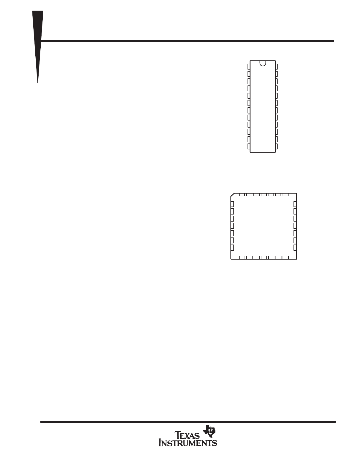
NT PACKAGE
(TOP VIEW)
NC
24
23
22
21
20
19
18
17
16
15
14
13
CC
V
I
V
CC
I/O/Q
I/O/Q
I/O/Q
I/O/Q
I/O/Q
I/O/Q
I/O/Q
I/O/Q
I/O/Q
I/O/Q
I
I/O/Q
25
24
23
22
21
20
19
I/O/Q
I/O/Q
CLK/I
GND
I
I
I
NC
I
I
I
– No internal connection
NC
Pin assignments in operating mode
1
I
2
I
3
I
4
I
5
I
6
I
7
I
8
I
9
I
10
I
11
12
FN PACKAGE
(TOP VIEW)
I
I
CLK/INCI/O/Q
3212827
426
5
6
7
8
9
10
11
12 13
14 15 16 1718
I
I
GND
I/O/Q
I/O/Q
I/O/Q
NC
I/O/Q
I/O/Q
I/O/Q
The TIBP AL22V10-10C is a programmable array logic device featuring high speed and functional equivalency
when compared to presently available devices. They are implemented with the familiar sum-of-products
(AND-OR) logic structure featuring the new concept “Programmable Output Logic Macrocell”. These
IMPACT-X circuits combine the latest Advanced Low-Power Schottky technology with proven titaniumtungsten fuses to provide reliable, high-performance substitutes for conventional TTL logic.
These devices contain up to 22 inputs and 10 outputs. They incorporate the unique capability of defining and
programming the architecture of each output on an individual basis. Outputs may be registered or nonregistered
and inverting or noninverting as shown in the output logic macrocell diagram. The ten potential outputs are
enabled through the use of individual product terms.
Further advantages can be seen in the introduction of variable product term distribution. This technique
allocates from 8 to 16 logical product terms to each output for an average of 12 product terms per output. This
variable allocation of terms allows far more complex functions to be implemented than in previously available
devices.
This device is covered by U.S. Patent 4,410,987.
IMPACT-X is a trademark of Texas Instruments Incorporated.
PRODUCTION DATA information is current as of publication date.
Products conform to specifications per the terms of Texas Instruments
standard warranty. Production processing does not necessarily include
testing of all parameters.
POST OFFICE BOX 655303 • DALLAS, TEXAS 75265
Copyright 1992, Texas Instruments Incorporated
1

TIBPAL22V10-10C
HIGH-PERFORMANCE IMPACT-X PROGRAMMABLE ARRAY LOGIC CIRCUITS
SRPS015 – D3972, FEBRUARY 1992
description (continued)
Circuit design is enhanced by the addition of a synchronous set and an asynchronous reset product term. These
functions are common to all registers. When the synchronous set product term is a logic 1, the output registers
are loaded with a logic 1 on the next low-to-high clock transition. When the asynchronous reset product term
is a logic 1, the output registers are loaded with a logic 0. The output logic level after set or reset depends on
the polarity selected during programming. Output registers can be preloaded to any desired state during testing.
Preloading permits full logical verification during product testing.
With features such as programmable output logic macrocells and variable product term distribution, the
TIBPAL22V10-10C offers quick design and development of custom LSI functions with complexities of 500 to
800 equivalent gates. Since each of the ten output pins may be individually configured as inputs on either a
temporary or permanent basis, functions requiring up to 21 inputs and a single output or down to 12 inputs and
10 outputs are possible.
A power-up clear function is supplied that forces all registered outputs to a predetermined state after power is
applied to the device. Registered outputs selected as active-low power up with their outputs high. Registered
outputs selected as active-high power up with their outputs low.
A single security fuse is provided on each device to discourage unauthorized copying of fuse patterns. Once
blown, the verification circuitry is disabled and all other fuses will appear to be open.
The TIBPAL22V10-10C is characterized for operation from 0°C to 75°C.
2
POST OFFICE BOX 655303 • DALLAS, TEXAS 75265
HIGH-PERFORMANCE IMPACT-X PROGRAMMABLE ARRAY LOGIC CIRCUITS
functional block diagram (positive logic)
TIBPAL22V10-10C
SRPS015 – D3972, FEBRUARY 1992
CLK/I
C1
1S
R
Output
Logic
Macrocell
EN
EN
EN
EN
EN
EN
EN
EN
EN
EN
I/O/Q
I/O/Q
I/O/Q
I/O/Q
I/O/Q
I/O/Q
I/O/Q
I/O/Q
I/O/Q
I/O/Q
10
10
12
14
16
16
14
12
10
Set
Reset
8
8
1
10
10
&
44 x 132
22
11
I
10
22
denotes fused inputs
POST OFFICE BOX 655303 • DALLAS, TEXAS 75265
3
4
POST OFFICE BOX 655303 • DALLAS, TEXAS 75265
logic diagram (positive logic)
1
CLK/I
First
Fuse
Numbers
I
I
2
3
0 4 8 1216202428
0
396
440
880
924
1452
1496
Increment
32 36 40
Macrocell
P = 5808
R = 5809
Macrocell
P = 5810
R = 5811
Macrocell
P = 5812
R = 5813
Macrocell
Asynchronous Reset
(to all registers)
23
I/O/Q
22
I/O/Q
21
I/O/Q
20
I/O/Q
SRPS015 – D3972, FEBRUARY 1992
TIBPAL22V10-10C
HIGH-PERFORMANCE IMPACT-X PROGRAMMABLE ARRAY LOGIC CIRCUITS
2112
4
I
2156
2860
5
I
P = 5814
R = 5815
Macrocell
P = 5816
R = 5817
19
I/O/Q
POST OFFICE BOX 655303 • DALLAS, TEXAS 75265
2904
Macrocell
18
I/O/Q
HIGH-PERFORMANCE IMPACT-X PROGRAMMABLE ARRAY LOGIC CIRCUITS
3608
6
I
3652
4268
7
I
4312
4840
8
I
4884
P = 5818
R = 5819
Macrocell
P = 5820
R = 5821
Macrocell
P = 5822
R = 5823
Macrocell
17
16
15
I/O/Q
I/O/Q
I/O/Q
5324
9
I
5368
5720
10
I
5764
11
I
P = 5824
R = 5825
Macrocell
P = 5826
R = 5827
14
I/O/Q
Synchronous Set
(to all registers)
13
I
SRPS015 – D3972, FEBRUARY 1992
TIBPAL22V10-10C
Fuse number = First Fuse number + Increment
5
Inside each MACROCELL the ”P” fuse is the polarity fuse and the ”R” fuse is the register fuse.
TIBPAL22V10-10C
HIGH-PERFORMANCE IMPACT-X PROGRAMMABLE ARRAY LOGIC CIRCUITS
SRPS015 – D3972, FEBRUARY 1992
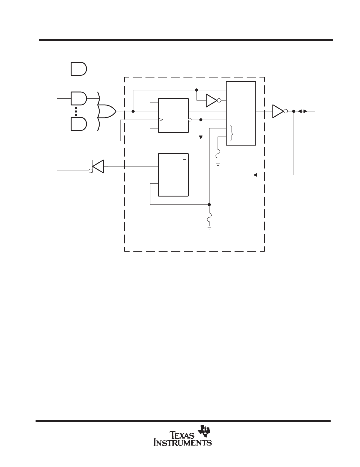
output logic macrocell diagram
Output Logic Macrocell
MUX
2
From Clock Buffer
I = 0
AR
SS
AR = asynchronous reset
SS = synchronous set
R
1D
C1
1S
MUX
1
1
G1
S1
S0
3
0
1
0
1
G
3
0
6
POST OFFICE BOX 655303 • DALLAS, TEXAS 75265

TIBPAL22V10-10C
HIGH-PERFORMANCE IMPACT-X PROGRAMMABLE ARRAY LOGIC CIRCUITS
SRPS015 – D3972, FEBRUARY 1992
R
1D
C1
1S
REGISTER FEEDBACK, REGISTERED, ACTIVE-LOW OUTPUT REGISTER FEEDBACK, REGISTERED, ACTIVE-HIGH OUTPUT
I/O FEEDBACK, COMBINATIONAL, ACTIVE-LOW OUTPUT I/O FEEDBACK, COMBINATIONAL, ACTIVE-HIGH OUTPUT
S1 = 0
S0 = 0
S1 = 1
S0 = 0
R
1D
1S
C1
S1 = 0
S0 = 1
S1 = 1
S0 = 1
MACROCELL FEEDBACK AND OUTPUT FUNCTION TABLE
FUSE SELECT
S1 S0
0 0 Register feedback Registered Active low
0 1 Register feedback Registered Active high
1 0 I/O feedback Combinational Active low
1 1 I/O feedback Combinational Active high
0 = unblown fuse, 1 = blown fuse
S1 and S0 are select-function fuses as shown in the output logic macrocell
diagram.
FEEDBACK AND OUTPUT CONFIGURATION
Figure 1. Resultant Macrocell Feedback and Output Logic After Programming
POST OFFICE BOX 655303 • DALLAS, TEXAS 75265
7

TIBPAL22V10-10C
HIGH-PERFORMANCE IMPACT-X PROGRAMMABLE ARRAY LOGIC CIRCUITS
SRPS015 – D3972, FEBRUARY 1992
absolute maximum ratings over operating free-air temperature range (unless otherwise noted)
Supply voltage, VCC (see Note 1) 7 V. . . . . . . . . . . . . . . . . . . . . . . . . . . . . . . . . . . . . . . . . . . . . . . . . . . . . . . . . . . .
Input voltage (see Note 1) –1.2 V to VCC +0.5 V. . . . . . . . . . . . . . . . . . . . . . . . . . . . . . . . . . . . . . . . . . . . . . . . . . . .
Voltage range applied to disabled output (see Note 1) –0.5 V to VCC +0.5 V. . . . . . . . . . . . . . . . . . . . . . . . . . .
Operating free-air temperature range 0°C to 75°C. . . . . . . . . . . . . . . . . . . . . . . . . . . . . . . . . . . . . . . . . . . . . . . . . .
Storage temperature range –65°C to 150°C. . . . . . . . . . . . . . . . . . . . . . . . . . . . . . . . . . . . . . . . . . . . . . . . . . . . . . .
NOTE 1: These ratings apply except for programming pins during a programming cycle or during a preload cycle.
recommended operating conditions
MIN NOM MAX UNIT
V
V
V
I
OH
I
OL
w
t
su
t
h
T
A
NOTE 2: These are absolute voltage levels with respect to the ground pin of the device and includes all overshoots due to system and/or tester
Supply voltage 4.75 5 5.25 V
CC
High-level input voltage (see Note 2) 2 5.5 V
IH
Low-level input voltage (see Note 2) 0.8 V
IL
High-level output current –3.2 mA
Low-level output current 16 mA
Pulse durationt
Setup time before clock↑ Synchronous preset (active) 9 ns
Hold time, input, set, or feedback after clock↑ 0 ns
Operating free-air temperature 0 75 °C
noise. Testing these parameters should not be attempted without suitable equipment.
Clock high or low 5
Asynchronous reset high or low 10
Input 7
Feedback 7
Synchronous preset (inactive) 8
Asynchronous reset (inactive) 8
ns
8
POST OFFICE BOX 655303 • DALLAS, TEXAS 75265

TIBPAL22V10-10C
HIGH-PERFORMANCE IMPACT-X PROGRAMMABLE ARRAY LOGIC CIRCUITS
SRPS015 – D3972, FEBRUARY 1992
electrical characteristics over recommended operating free-air temperature range
PARAMETER TEST CONDITIONS MIN TYP†MAX UNIT
V
IK
V
OH
V
OL
‡
I
OZH
‡
I
OZL
I
I
‡
I
IH
I
IL
I
OS
I
CC
C
i
C
o
†
All typical values are at VCC = 5 V, TA = 25°C.
‡
I/O leakage is the worst case of I
§
Not more than one output should be shorted at a time, and the duration of the short circuit should not exceed one second. VO is set at 0.5 V to
avoid test problems caused by test equipment ground degradation.
CLK –0.25
All others –0.1
§
I 6
CLK 6
VCC = 4.75 V, II = –18 mA –1.2 V
VCC = 4.75 V, IOH = –3.2 mA 2.4 V
VCC = 4.75 V, IOL = 16 mA 0.35 0.5 V
VCC = 5.25 V, VO = 2.7 V 0.1 mA
VCC = 5.25 V, VO = 0.4 V –0.1 mA
VCC = 5.25 V, VI = 5.5 V 1 mA
VCC = 5.25 V, VI = 2.7 V 25 µA
VCC = 5.25 V, VI = 0.4 V
VCC = 5.25 V, VO = 0.5 V –30 –130 mA
VCC = 5.25 V, VI = GND, Outputs open 210 mA
f = 1 MHz, VI = 2 V
f = 1 MHz, VO = 2 V 8 pF
and IIL or I
OZL
and IIH, respectively.
OZH
mA
pF
switching characteristics over recommended ranges of supply voltage and operating free-air
temperature (unless otherwise noted)
PARAMETER
¶
f
max
t
pd
t
pd
t
pd
#
t
pd
t
en
t
dis
¶
f
(without feedback) =
max
f
(with internal feedback) =
max
f
(with external feedback) =
max
#
This parameter is calculated from the measured f
FROM
(INPUT)
Without feedback 100
With internal feedback (counter configuration) 80 MHz
With external feedback 71
I, I/O I/O R1 = 300 Ω, 1 10 ns
I, I/O (reset) Q R2 = 300 Ω, 15 ns
CLK Q See Figure 6 1 7 ns
CLK Feedback 5.5 ns
I, I/O I/O, Q 11 ns
I, I/O I/O, Q 9 ns
tw(low))tw(high)
1
tsu)
tpd(CLK to feedback)
tsu)
1
tpd(CLK to Q)
1
TO
(OUTPUT)
with internal feedback in the counter configuration.
max
TEST CONDITION MIN MAX UNIT
POST OFFICE BOX 655303 • DALLAS, TEXAS 75265
9

TIBPAL22V10-10C
HIGH-PERFORMANCE IMPACT-X PROGRAMMABLE ARRAY LOGIC CIRCUITS
SRPS015 – D3972, FEBRUARY 1992
preload procedure for registered outputs (see Notes 3 and 4)
The output registers can be preloaded to any desired state during device testing. This permits any state to be
tested without having to step through the entire state-machine sequence. Each register is preloaded individually
by following the steps given below:
Step 1. With VCC at 5 V and pin 1 at VIL, raise pin 13 to V
IHH
.
Step 2. Apply either VIL or VIH to the output corresponding to the register to be preloaded.
Step 3. Pulse pin 1, clocking in preload data.
Step 4. Remove output voltage, then lower pin 13 to V
. Preload can be verified by observing the voltage level
IL
at the output pin.
V
V
V
V
V
V
IHH
IL
IH
IL
OH
OL
Pin 13
t
t
d
Pin 1
Registered I/O Input Output
su
t
w
t
d
V
IH
V
IL
Figure 2. Preload Waveforms
NOTES: 3. Pin numbers shown are for the NT package only. If chip-carrier socket adapter is not used, pin numbers must be changed accordingly .
t
t
tw = 100 ns to 1000 ns. V
4.
=
=
d
su
= 10.25 V to 10.75 V.
IHH
10
POST OFFICE BOX 655303 • DALLAS, TEXAS 75265

TIBPAL22V10-10C
HIGH-PERFORMANCE IMPACT-X PROGRAMMABLE ARRAY LOGIC CIRCUITS
SRPS015 – D3972, FEBRUARY 1992
power-up reset
Following power up, all registers are reset to zero. The output level depends on the polarity selected during
programming. This feature provides extra flexibility to the system designer and is especially valuable in
simplifying state-machine initialization. To ensure a valid power-up reset, it is important that the rise of VCC be
monotonic. Following power-up reset, a low-to-high clock transition must not occur until all applicable input and
feedback setup times are met.
V
CC
Active High
Registered Output
Active Low
Registered Output
CLK
4 V
†
tpd
(600 ns typ, 1000 ns MAX)
State Unknown
State Unknown
1.5 V
1.5 V
1.5 V
tsu
t
w
‡
1.5 V
5 V
V
V
V
V
V
V
OH
OL
OH
OL
IH
IL
†
This is the power-up reset time and applies to registered outputs only. The values shown are from characterization data.
‡
This is the setup time for input or feedback.
Figure 3. Power-Up Reset Waveforms
programming information
Texas Instruments programmable logic devices can be programmed using widely available software and
inexpensive device programmers.
Complete programming specifications, algorithms, and the latest information on hardware, software, and
firmware are available upon request. Information on programmers capable of programming T exas Instruments
programmable logic is also available, upon request, from the nearest TI field sales office, local authorized TI
distributor, or by calling Texas Instruments at (214) 997-5666.
POST OFFICE BOX 655303 • DALLAS, TEXAS 75265
11

TIBPAL22V10-10C
HIGH-PERFORMANCE IMPACT-X PROGRAMMABLE ARRAY LOGIC CIRCUITS
SRPS015 – D3972, FEBRUARY 1992
THERMAL INFORMATION
thermal management of the TIBPAL22V10-10C
Thermal management of the TIBP AL22V10-10CNT and TIBP AL22V10-10CFN is necessary when operating at
certain conditions of frequency , output loading, and outputs switching simultaneously. The device and system
application will determine the appropriate level of management.
Determining the level of thermal management is based on factors such as power dissipation (P
), ambient
D
temperature (TA), and transverse airflow (FPM). Figures 4 (a) and 4 (b) show the relationship between ambient
temperature and transverse airflow at given power dissipation levels. The required transverse airflow can be
determined at a particular ambient temperature and device power dissipation level in order to ensure the device
specifications.
Figure 5 illustrates how power dissipation varies as a function of frequency and the number of outputs switching
simultaneously . It should be noted that all outputs are fully loaded (C
= 50 pF). Since the condition of eight fully
L
loaded outputs represents the worst-case condition, each application must be evaluated accordingly.
MINIMUM TRANSVERSE AIR FLOW
600
500
400
300
200
100
Minimum Transverse Air Flow – ft/min
vs
AMBIENT TEMPERATURE
PD = 1.6 W
PD = 1.4 W
PD = 1.2 W
PD = 1 W
600
500
400
300
200
100
Minimum Transverse Air Flow – ft/min
MINIMUM TRANSVERSE AIR FLOW
vs
AMBIENT TEMPERATURE
PD = 1.6 W
PD = 1.4 W
PD = 1.2 W
PD = 1 W
12
0
TA – Ambient Temperature –°C
(a) TIBPAL22V10-10CNT
30
4020100
60 70
8050
0
TA – Ambient Temperature –°C
(b) TIBPAL22V10-10CFN
30
4020100
60 70
8050
Figure 4
POST OFFICE BOX 655303 • DALLAS, TEXAS 75265

TIBPAL22V10-10C
HIGH-PERFORMANCE IMPACT-X PROGRAMMABLE ARRAY LOGIC CIRCUITS
SRPS015 – D3972, FEBRUARY 1992
THERMAL INFORMATION
POWER DISSIPATION
vs
FREQUENCY
2000
VCC = 5 V
TA = 25 °C
CL = 50 pF
1800
1600
1400
1200
– Power Dissipation – mW
D
P
1000
10 Outputs Switching
1 Output Switching
800
1 4 10 40 1002 20 200
f – Frequency – MHz
Figure 5
POST OFFICE BOX 655303 • DALLAS, TEXAS 75265
13

TIBPAL22V10-10C
HIGH-PERFORMANCE IMPACT-X PROGRAMMABLE ARRAY LOGIC CIRCUITS
SRPS015 – D3972, FEBRUARY 1992
PARAMETER MEASUREMENT INFORMATION
5 V
S1
R1
From Output
Under Test
Test
Point
Timing
Input
t
Data
Input
Input
t
pd
In-Phase
Output
t
pd
Out-of-Phase
Output
(see Note D)
PROPAGATION DELAY TIMES
1.5 V
su
1.5 V
VOLTAGE WAVEFORMS
SETUP AND HOLD TIMES
1.5 V 1.5 V
1.5 V
1.5 V 1.5 V
VOLTAGE WAVEFORMS
(see Note A)
t
h
1.5 V
3 V
0
3 V
0
(see Note B)
3 V
0
t
pd
V
1.5 V
V
t
pd
V
V
C
L
LOAD CIRCUIT FOR
3-STATE OUTPUTS
OH
OL
OH
OL
R2
High-Level
Pulse
Low-Level
Pulse
Output
Control
(low-level
enabling)
Waveform 1
S1 Closed
(see Note C)
Waveform 2
S1 Open
(see Note C)
1.5 V 1.5 V
t
w
1.5 V 1.5 V
VOLTAGE WAVEFORMS
PULSE DURATIONS
1.5 V 1.5 V
t
en
t
en
t
1.5 V
t
1.5 V
dis
dis
3 V
0
3 V
0
(see Note B)
3 V
0
(see Note B)
≈ 2.7 V
VOL + 0.5 V
V
OL
V
OH
VOH – 0.5 V
≈ 0 V
ENABLE AND DISABLE TIMES, 3-STATE OUTPUTS
NOTES: A. CL includes probe and jig capacitance and is 50 pF for tpd and ten, 5 pF for t
B. All input pulses have the following characteristics: PRR ≤ 1 MHz, tr = tf = 2 ns, duty cycle = 50%.
C. Waveform 1 is for an output with internal conditions such that the output is low except when disabled by the output control. Waveform 2
is for an output with internal conditions such that the output is high except when disabled by the output control.
D. When measuring propagation delay times of 3-state outputs, switch S1 is closed.
E. Equivalent loads may be used for testing.
Figure 6. Load Circuit and Voltage Waveforms
14
POST OFFICE BOX 655303 • DALLAS, TEXAS 75265
VOLTAGE WAVEFORMS
.
dis

TIBPAL22V10-10C
HIGH-PERFORMANCE IMPACT-X PROGRAMMABLE ARRAY LOGIC CIRCUITS
SRPS015 – D3972, FEBRUARY 1992
TYPICAL CHARACTERISTICS
SUPPLY CURRENT
vs
FREE-AIR TEMPERATURE
220
210
VCC = 5.25 V
200
VCC = 5 V
– Supply Current – mA
CC
190
I
180
VCC = 4.75 V
02550
TA – Free-Air Temperature – °C
Figure 7
75
PROPAGATION DELAY TIME
7
6
5
t
PLH
4
t
PHL
3
2
Propagation Delay Time – ns
TA = 25 °C
CL = 50 pF
R1 = 300 Ω
1
R2 = 300 Ω
10 Outputs Switching
0
4.75 5
vs
SUPPLY VOLTAGE
t
(I, I/O to O, I/O)
PLH
t
(I, I/O to O, I/O)
PHL
(CLK to Q)
(CLK to Q)
VCC – Supply Voltage – V
Figure 8
5.25
PROPAGATION DELAY TIME
vs
FREE-AIR TEMPERATURE
7
t
(I, I/O to O, I/O)
6
5
t
PLH
4
3
2
Propagation Delay Time – ns
VCC = 5 V
CL = 50 pF
R1 = 300 Ω
1
R2 = 300 Ω
10 Output Switching
0
02550
t
(CLK to Q)
TA – Free-Air Temperature – °C
PLH
(I, I/O to O, I/O)
PHL
t
PHL
Figure 9
(CLK to Q)
75
16
14
12
10
– Propagation Delay Time – ns
pd
t
PROPAGATION DELAY TIME
vs
LOAD CAPACITANCE
VCC = 5 V
TA = 25 °C
R1 = 300 Ω
R2 = 300 Ω
1 Output Switching
8
6
tpd (CLK to Q)
4
2
0
0 600
100 200 300 400
CL – Load Capacitance – pF
tpd (I, I/O to O, I/O)
500
Figure 10
POST OFFICE BOX 655303 • DALLAS, TEXAS 75265
15

TIBPAL22V10-10C
HIGH-PERFORMANCE IMPACT-X PROGRAMMABLE ARRAY LOGIC CIRCUITS
SRPS015 – D3972, FEBRUARY 1992
TYPICAL CHARACTERISTICS
POWER DISSIPATION
PROPAGATION DELAY TIME
vs
NUMBER OF OUTPUTS SWITCHING
7
6
5
10-BIT COUNTER MODE
1200
VCC = 5 V
1150
vs
FREQUENCY
4
3
Propagation Delay Time – ns
VCC = 5 V
TA = 25 °C
2
CL = 50 pF
R1 = 300 Ω
R2 = 300 Ω
1
12345
Number of Outputs Switching
Figure 11
= t
(I, I/O to O, I/O)
PLH
= t
(I, I/O to O, I/O)
PHL
= t
(CLK to Q)
PLH
= t
(CLK to Q)
PHL
67
6710
1100
– Power Dissipation – mW
D
1050
P
1000
TA = 80 °C
1 4 10 40 100
TA = 0 °C
220
f – Frequency – MHz
Figure 12
TA = 25 °C
16 SRPS015
POST OFFICE BOX 655303 • DALLAS, TEXAS 75265

IMPORTANT NOTICE
T exas Instruments and its subsidiaries (TI) reserve the right to make changes to their products or to discontinue
any product or service without notice, and advise customers to obtain the latest version of relevant information
to verify, before placing orders, that information being relied on is current and complete. All products are sold
subject to the terms and conditions of sale supplied at the time of order acknowledgement, including those
pertaining to warranty, patent infringement, and limitation of liability.
TI warrants performance of its semiconductor products to the specifications applicable at the time of sale in
accordance with TI’s standard warranty. Testing and other quality control techniques are utilized to the extent
TI deems necessary to support this warranty . Specific testing of all parameters of each device is not necessarily
performed, except those mandated by government requirements.
CERTAIN APPLICA TIONS USING SEMICONDUCT OR PRODUCTS MAY INVOLVE POTENTIAL RISKS OF
DEATH, PERSONAL INJURY, OR SEVERE PROPERTY OR ENVIRONMENTAL DAMAGE (“CRITICAL
APPLICATIONS”). TI SEMICONDUCTOR PRODUCTS ARE NOT DESIGNED, AUTHORIZED, OR
WARRANTED TO BE SUITABLE FOR USE IN LIFE-SUPPORT DEVICES OR SYSTEMS OR OTHER
CRITICAL APPLICA TIONS. INCLUSION OF TI PRODUCTS IN SUCH APPLICATIONS IS UNDERST OOD TO
BE FULLY AT THE CUSTOMER’S RISK.
In order to minimize risks associated with the customer’s applications, adequate design and operating
safeguards must be provided by the customer to minimize inherent or procedural hazards.
TI assumes no liability for applications assistance or customer product design. TI does not warrant or represent
that any license, either express or implied, is granted under any patent right, copyright, mask work right, or other
intellectual property right of TI covering or relating to any combination, machine, or process in which such
semiconductor products or services might be or are used. TI’s publication of information regarding any third
party’s products or services does not constitute TI’s approval, warranty or endorsement thereof.
Copyright 1998, Texas Instruments Incorporated
 Loading...