

TEXAS INSTRUMENTS TIBPAL16L8-5C, TIBPAL16R4-5C, TIBPAL16R6-5C, TIBPAL16R8-5C, TIBPAL16L8-7M Technical data
...
查询5962-8515521RA供应商
TIBPAL16L8-5C, TIBPAL16R4-5C, TIBPAL16R6-5C, TIBPAL16R8-5C
TIBPAL16L8-7M, TIBPAL16R4-7M, TIBPAL16R6-7M, TIBPAL16R8-7M
HIGH-PERFORMANCE IMPACT-X PAL
SRPS011D – D3359, OCTOBER 1989 – REVISED SEPTEMBER 1992
CIRCUITS
• High-Performance Operation:
f
(no feedback)
max
TIBPAL16R’ -5C Series . . . 125 MHz Min
TIBPAL16R’ -7M Series . . . 100 MHz Min
f
(internal feedback)
max
TIBPAL16R’ -5C Series . . . 125 MHz Min
TIBPAL16R’ -7M Series . . . 100 MHz Min
f
(external feedback)
max
TIBPAL16R’ -5C Series . . . 117 MHz Min
TIBPAL16R’ -7M Series . . . 74 MHz Min
Propagation Delay
TIBPAL16L8-5C Series . . . 5 ns Max
TIBPAL16L8-7M Series . . . 7 ns Max
TIBPAL16R’ -5C Series
(CLK-to-Q) . . . 4 ns Max
TIBPAL16R ’ -7M Series
(CLK-to-Q) . . . 6.5 ns Max
• Functionally Equivalent, but Faster than,
Existing 20-Pin PLDs
• Preload Capability on Output Registers
Simplifies Testing
• Power-Up Clear on Registered Devices (All
Register Outputs are Set Low, but Voltage
Levels at the Output Pins Go High)
TIBPAL16L8’
C SUFFIX . . . J OR N PACKAGE
M SUFFIX . . . J PACKAGE
(TOP VIEW)
I
1
I
2
I
3
I
4
I
5
I
6
I
7
I
8
I
9
GND
C SUFFIX . . . FN PACKAGE
M SUFFIX . . . FK PACKAGE
10
TIBPAL16L8’
(TOP VIEW)
I
I
V
20
CC
O
19
I/O
18
I/O
17
I/O
16
15
I/O
14
I/O
13
I/O
12
O
11
I
CC
I
O
V
• Package Options Include Both Plastic and
Ceramic Chip Carriers in Addition to Plastic
and Ceramic DIPs
• Security Fuse Prevents Duplication
DEVICE
’PAL16L8 10 2 0 6
’PAL16R4 8 0 4 (3-state buffers) 4
’PAL16R6 8 0 6 (3-state buffers) 2
’PAL16R8 8 0 8 (3-state buffers) 0
I
INPUTS
3-STATE
O OUTPUTS
REGISTERED
Q OUTPUTS
I/O
PORT
S
3 2 1 20 19
I
4
I
5
I
6
I
7
I
8
910111213
I
I
O
18
17
16
15
14
I/O
I/O
I/O
I/O
I/O
I/O
GND
Pin assignments in operating mode
description
These programmable array logic devices feature high speed and functional equivalency when compared with
currently available devices. These IMPACT-X circuits combine the latest Advanced Low-Power Schottky
technology with proven titanium-tungsten fuses to provide reliable, high-performance substitutes for
conventional TTL logic. Their easy programmability allows for quick design of custom functions and typically
results in a more compact circuit board.
The TIBPAL16’ C series is characterized from 0°C to 75°C. The TIBPAL16’ M series is characterized for
operation over the full military temperature range of –55°C to 125°C.
These devices are covered by U.S. Patent 4,410,987.
IMPACT-X is a trademark of Texas Instruments Incorporated.
PAL is a registered trademark of Advanced Micro Devices Inc.
This document contains information on products in more than one phase
of development. The status of each device is indicated on the page(s)
specifying its electrical characteristics.
POST OFFICE BOX 655303 • DALLAS, TEXAS 75265
Copyright 1992, Texas Instruments Incorporated
1

TIBPAL16R4-5C, TIBPAL16R6-5C, TIBPAL16R8-5C
TIBPAL16R4-7M, TIBPAL16R6-7M, TIBPAL16R8-7M
HIGH-PERFORMANCE IMPACT-X PAL
SRPS011D – D3359, OCTOBER 1989 – REVISED SEPTEMBER 1992
CIRCUITS
TIBPAL16R4 ’
C SUFFIX . . . J OR N PACKAGE
M SUFFIX . . . J PACKAGE
(TOP VIEW)
CLK
1
I
2
I
3
I
4
I
5
I
6
I
7
I
8
I
9
GND
C SUFFIX . . . J OR N PACKAGE
M SUFFIX . . . J PACKAGE
GND
CLK
I
I
I
I
I
I
I
I
10
TIBPAL16R6 ’
(TOP VIEW)
1
2
3
4
5
6
7
8
9
10
20
19
18
17
16
15
14
13
12
11
20
19
18
17
16
15
14
13
12
11
V
I/O
I/O
Q
Q
Q
Q
I/O
I/O
OE
V
I/O
Q
Q
Q
Q
Q
Q
I/O
OE
CC
CC
TIBPAL16R4 ’
C SUFFIX . . . FN PACKAGE
M SUFFIX . . . FK PACKAGE
(TOP VIEW)
CC
I
CLK
I/O
V
18
17
16
15
14
3 2 1 20 19
I
4
I
5
I
6
I
7
I
8
910111213
I
I
I/O
I/O
OE
GND
TIBPAL16R6 ’
C SUFFIX . . . FN PACKAGE
M SUFFIX . . . FK PACKAGE
(TOP VIEW)
I
GND
CLK
OE
CC
V
I/O
I/O
18
17
16
15
14
Q
3 2 1 20 19
I
4
I
5
I
6
I
7
I
8
910111213
I
I
I/O
Q
Q
Q
Q
Q
Q
Q
Q
Q
C SUFFIX . . . J OR N PACKAGE
M SUFFIX . . . J PACKAGE
CLK
I
I
I
I
I
I
I
I
GND
Pin assignments in operating mode
2
TIBPAL16R8 ’
(TOP VIEW)
20
1
19
2
18
3
17
4
16
5
15
6
14
7
13
8
12
9
11
10
V
CC
Q
Q
Q
Q
Q
Q
Q
Q
OE
POST OFFICE BOX 655303 • DALLAS, TEXAS 75265
TIBPAL16R8 ’
C SUFFIX . . . FN PACKAGE
M SUFFIX . . . FK PACKAGE
(TOP VIEW)
I
GND
CLK
OE
CC
V
Q
Q
18
17
16
15
14
Q
3 2 1 20 19
I
4
I
5
I
6
I
7
I
8
910111213
I
I
Q
Q
Q
Q
Q
functional block diagrams (positive logic)
TIBPAL16L8-5C, TIBPAL16R4-5C
TIBPAL16L8-7M, TIBPAL16R4-7M
HIGH-PERFORMANCE IMPACT-X PAL
SRPS011D – D3359, OCTOBER 1989 – REVISED SEPTEMBER 1992
TIBPAL16L8’
CIRCUITS
OE
CLK
10 16
I
16 x
&
32 X 64
166
TIBPAL16R4’
7
7
7
7
7
7
7
7
6
EN
≥1
O
O
I/O
I/O
I/O
I/O
I/O
I/O
EN 2
C1
denotes fused inputs
816
I
16 x
4
164
&
32 X 64
1D
I = 0
2
Q
Q
Q
Q
I/O
I/O
I/O
I/O
8
8
8
8
7
7
7
7
4
≥1
≥1
EN
4
POST OFFICE BOX 655303 • DALLAS, TEXAS 75265
3
TIBPAL16R6-5C, TIBPAL16R8-5C
TIBPAL16R6-7M, TIBPAL16R8-7M
HIGH-PERFORMANCE IMPACT-X PAL
SRPS011D – D3359, OCTOBER 1989 – REVISED SEPTEMBER 1992
functional block diagrams (positive logic)
CIRCUITS
TIBPAL16R6’
OE
CLK
816
I
16 x
6
162
&
32 X 64
EN 2
C1
1D
I = 0
2
Q
Q
Q
Q
Q
Q
I/O
I/O
8
8
8
8
8
8
7
7
2
≥1
≥1
EN
6
CLK
denotes fused inputs
OE
816
I
16 x
168
TIBPAL16R8’
&
32 X 64
EN 2
C1
1D
I = 0
2
Q
Q
Q
Q
Q
Q
Q
Q
8
8
8
8
8
8
8
8
8
≥1
4
POST OFFICE BOX 655303 • DALLAS, TEXAS 75265
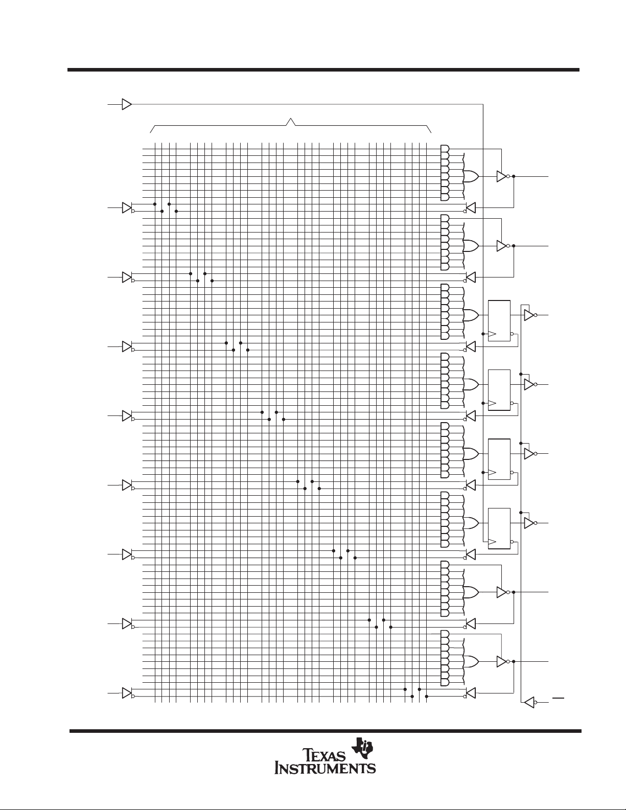
logic diagram (positive logic)
1
I
FIRST
FUSE
NUMBERS
2
I
3
I
4
I
5
I
6
I
7
I
8
I
9
I
0 4 8 12 16 20 24 28 31
0
32
64
96
128
160
192
224
256
288
320
352
384
416
448
480
512
544
576
608
640
672
704
736
768
800
832
864
896
928
960
992
1024
1056
1088
1120
1152
1184
1216
1248
1280
1312
1344
1376
1408
1440
1472
1504
1536
1568
1600
1632
1664
1696
1728
1760
1792
1824
1856
1888
1920
1952
1984
2016
HIGH-PERFORMANCE IMPACT-X PAL
SRPS011D – D3359, OCTOBER 1989 – REVISED SEPTEMBER 1992
INCREMENT
TIBPAL16L8-5C
TIBPAL16L8-7M
CIRCUITS
19
O
18
I/O
17
I/O
16
I/O
15
I/O
14
I/O
13
I/O
12
O
11
I
Fuse number = First fuse number + Increment
POST OFFICE BOX 655303 • DALLAS, TEXAS 75265
5
TIBPAL16R4-5C
TIBPAL16R4-7M
HIGH-PERFORMANCE IMPACT-X PAL
SRPS011D – D3359, OCTOBER 1989 – REVISED SEPTEMBER 1992
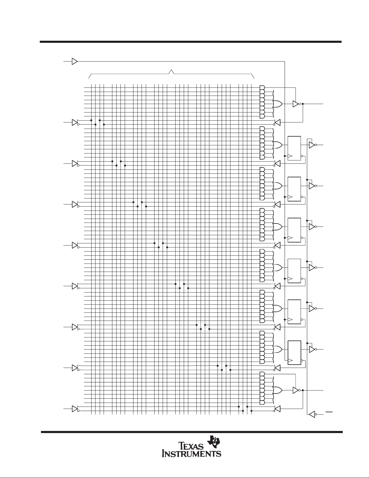
logic diagram (positive logic)
1
CLK
FIRST
FUSE
NUMBERS
2
I
3
I
4
I
5
I
6
I
7
I
8
I
9
I
0 4812 16 20 24 28 31
0
32
64
96
128
160
192
224
256
288
320
352
384
416
448
480
512
544
576
608
640
672
704
736
768
800
832
864
896
928
960
992
1024
1056
1088
1120
1152
1184
1216
1248
1280
1312
1344
1376
1408
1440
1472
1504
1536
1568
1600
1632
1664
1696
1728
1760
1792
1824
1856
1888
1920
1952
1984
2016
Fuse number = First fuse number + Increment
INCREMENT
CIRCUITS
I = 0
1D
I = 0
1D
I = 0
1D
I = 0
1D
C1
C1
C1
C1
19
18
17
16
15
14
13
12
11
I/O
I/O
Q
Q
Q
Q
I/O
I/O
OE
6
POST OFFICE BOX 655303 • DALLAS, TEXAS 75265
logic diagram (positive logic)
1
CLK
FIRST
FUSE
NUMBERS
2
I
3
I
4
I
5
I
6
I
7
I
8
I
9
I
Fuse number = First fuse number + Increment
0 4 8 12 16 20 24 28 31
0
32
64
96
128
160
192
224
256
288
320
352
384
416
448
480
512
544
576
608
640
672
704
736
768
800
832
864
896
928
960
992
1024
1056
1088
1120
1152
1184
1216
1248
1280
1312
1344
1376
1408
1440
1472
1504
1536
1568
1600
1632
1664
1696
1728
1760
1792
1824
1856
1888
1920
1952
1984
2016
HIGH-PERFORMANCE IMPACT-X PAL
SRPS011D – D3359, OCTOBER 1989 – REVISED SEPTEMBER 1992
INCREMENT
TIBPAL16R6-5C
TIBPAL16R6-7M
CIRCUITS
19
I/O
I = 0
1D
C1
I = 0
1D
C1
I = 0
1D
C1
I = 0
1D
C1
I = 0
1D
C1
I = 0
1D
C1
18
17
16
15
14
13
12
11
Q
Q
Q
Q
Q
Q
I/O
OE
POST OFFICE BOX 655303 • DALLAS, TEXAS 75265
7
TIBPAL16R8-5C
TIBPAL16R8-7M
HIGH-PERFORMANCE IMPACT-X PAL
SRPS011D – D3359, OCTOBER 1989 – REVISED SEPTEMBER 1992
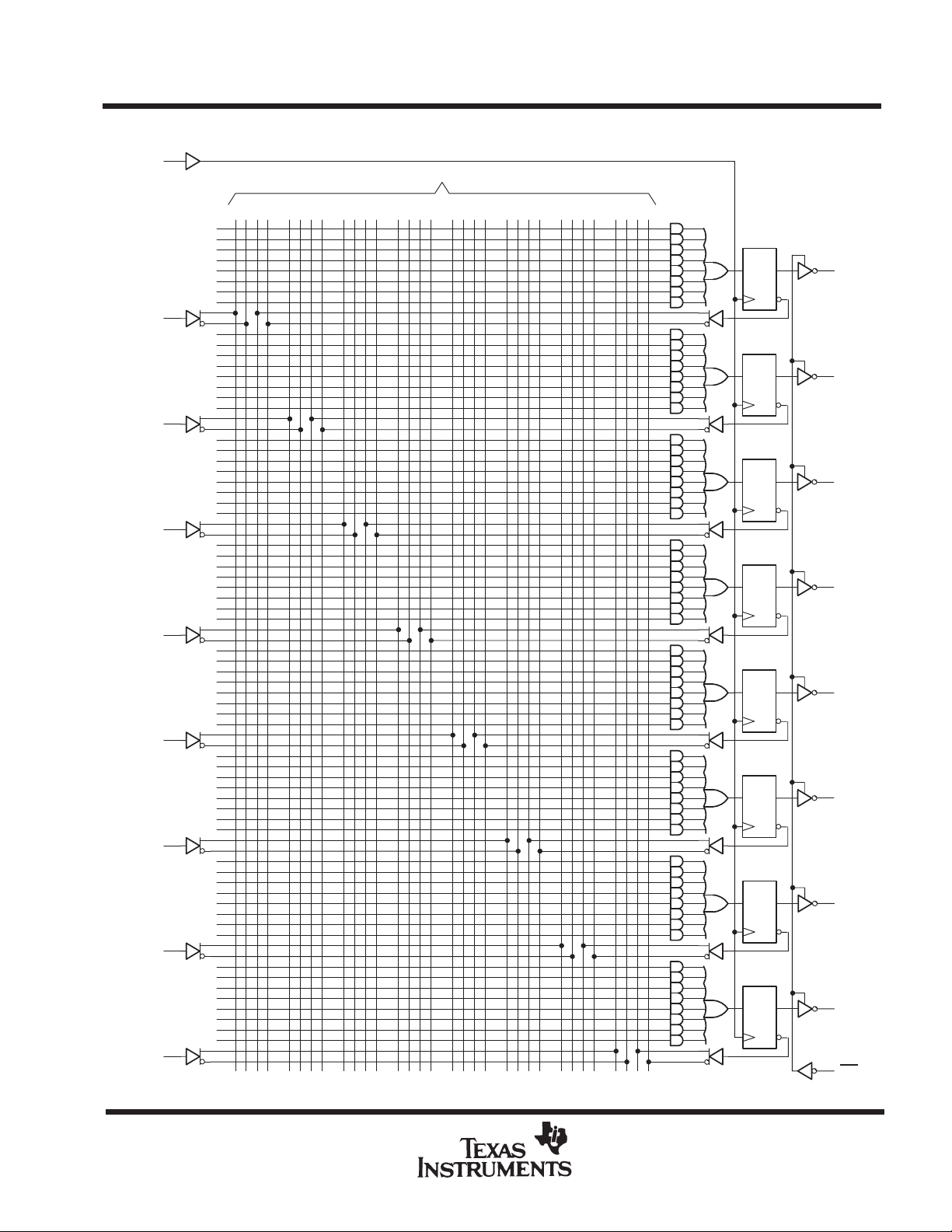
logic diagram (positive logic)
1
CLK
FIRST
FUSE
NUMBERS
2
I
3
I
4
I
5
I
6
I
7
I
8
I
9
I
0 4 8 12 16 20 24 28 31
0
32
64
96
128
160
192
224
256
288
320
352
384
416
448
480
512
544
576
608
640
672
704
736
768
800
832
864
896
928
960
992
1024
1056
1088
1120
1152
1184
1216
1248
1280
1312
1344
1376
1408
1440
1472
1504
1536
1568
1600
1632
1664
1696
1728
1760
1792
1824
1856
1888
1920
1952
1984
2016
Fuse number = First fuse number + Increment
INCREMENT
CIRCUITS
I = 0
1D
I = 0
1D
I = 0
1D
I = 0
1D
I = 0
1D
I = 0
1D
I = 0
1D
I = 0
1D
C1
C1
C1
C1
C1
C1
C1
C1
19
18
17
16
15
14
13
12
11
Q
Q
Q
Q
Q
Q
Q
Q
OE
8
POST OFFICE BOX 655303 • DALLAS, TEXAS 75265

TIBPAL16L8-5C
HIGH-PERFORMANCE IMPACT-X PAL
SRPS011D – D3359, OCTOBER 1989 – REVISED SEPTEMBER 1992
absolute maximum ratings over operating free-air temperature range (unless otherwise noted)
Supply voltage, VCC (see Note 1) 7 V. . . . . . . . . . . . . . . . . . . . . . . . . . . . . . . . . . . . . . . . . . . . . . . . . . . . . . . . . . . .
Input voltage (see Note 1) 5.5 V. . . . . . . . . . . . . . . . . . . . . . . . . . . . . . . . . . . . . . . . . . . . . . . . . . . . . . . . . . . . . . . . . .
Voltage applied to disabled output (see Note 1) 5.5 V. . . . . . . . . . . . . . . . . . . . . . . . . . . . . . . . . . . . . . . . . . . . . . .
Operating free-air temperature range 0°C to 75°C. . . . . . . . . . . . . . . . . . . . . . . . . . . . . . . . . . . . . . . . . . . . . . . . . .
Storage temperature range –65°C to 150°C. . . . . . . . . . . . . . . . . . . . . . . . . . . . . . . . . . . . . . . . . . . . . . . . . . . . . . .
NOTE 1: These ratings apply except for programming pins during a programming cycle or during a preload cycle.
recommended operating conditions
MIN NOM MAX UNIT
V
CC
V
IH
V
IL
I
OH
I
OL
T
A
NOTE 2: These are absolute voltage levels with respect to the ground pin of the device and include all overshoots due to system and/or tester
Supply voltage 4.75 5 5.25 V
High-level input voltage (see Note 2) 2 5.5 V
Low-level input voltage (see Note 2) 0.8 V
High-level output current –3.2 mA
Low-level output current 24 mA
Operating free-air temperature 0 25 75 °C
noise. Testing these parameters should not be attempted without suitable equipment.
CIRCUITS
electrical characteristics over recommended operating free-air temperature range
PARAMETER TEST CONDITIONS MIN TYP†MAX UNIT
V
IK
V
OH
V
OL
‡
I
OZH
‡
I
OZL
I
I
‡
I
IH
‡
I
IL
§
I
OS
I
CC
C
i
C
o
†
All typical values are at VCC = 5 V, TA = 25°C.
‡
I/O leakage is the worst case of I
§
Not more than one output should be shorted at a time, and the duration of the short circuit should not exceed one second. VO is set at 0.5 V to
avoid test problems caused by test equipment ground degradation.
VCC = 4.75 V, II = –18 mA –0.8 –1.5 V
VCC = 4.75 V, IOH = –3.2 mA 2.4 2.7 V
VCC = 4.75 V, IOL = 24 mA 0.3 0.5 V
VCC = 5.25 V, VO = 2.7 V 100 µA
VCC = 5.25 V, VO = 0.4 V –100 µA
VCC = 5.25 V, VI = 5.5 V 100 µA
VCC = 5.25 V, VI = 2.7 V 25 µA
VCC = 5.25 V, VI = 0.4 V –250 µA
VCC = 5.25 V, VO = 0.5 V –30 –70 –130 mA
VCC = 5.25 V, VI = 0, Outputs open 180 mA
f = 1 MHz, VI = 2 V 8.5 pF
f = 1 MHz, VO = 2 V 10 pF
and IIL or I
OZL
and IIH, respectively.
OZH
switching characteristics over recommended ranges of supply voltage and operating free-air
temperature (unless otherwise noted)
FROM
(INPUT)
I, I/O O, I/O
t
pd
t
en
t
dis
I, I/O O, I/O
I, I/O O, I/O 2 7 2 7 ns
I, I/O O, I/O 2 7 2 7 ns
TO
(OUTPUT)
with up to 4 outputs
switching
with more than 4
outputs switching
TEST
CONDITIONS
R1 = 200 Ω,
R2 = 200 Ω,
See Figure 8
TIBPAL16L8-5CFN
MIN MAX MIN MAX
1.5 5 1.5 5
1.5 5 1.5 5.5
TIBPAL16L8-5CJ
TIBPAL16L8-5CN
UNITPARAMETER
ns
PRODUCTION DATA information is current as of publication date.
Products conform to specifications per the terms of Texas Instruments
standard warranty. Production processing does not necessarily
include testing of all parameters.
POST OFFICE BOX 655303 • DALLAS, TEXAS 75265
9

TIBPAL16R4-5C, TIBPAL16R6-5C
HIGH-PERFORMANCE IMPACT-X PAL
SRPS011D – D3359, OCTOBER 1989 – REVISED SEPTEMBER 1992
absolute maximum ratings over operating free-air temperature range (unless otherwise noted)
Supply voltage, VCC (see Note 1) 7 V. . . . . . . . . . . . . . . . . . . . . . . . . . . . . . . . . . . . . . . . . . . . . . . . . . . . . . . . . . . .
Input voltage (see Note 1) 5.5 V. . . . . . . . . . . . . . . . . . . . . . . . . . . . . . . . . . . . . . . . . . . . . . . . . . . . . . . . . . . . . . . . . .
Voltage applied to disabled output (see Note 1) 5.5 V. . . . . . . . . . . . . . . . . . . . . . . . . . . . . . . . . . . . . . . . . . . . . . .
Operating free-air temperature range 0°C to 75°C. . . . . . . . . . . . . . . . . . . . . . . . . . . . . . . . . . . . . . . . . . . . . . . . . .
Storage temperature range –65°C to 150°C. . . . . . . . . . . . . . . . . . . . . . . . . . . . . . . . . . . . . . . . . . . . . . . . . . . . . . .
NOTE 1: These ratings apply except for programming pins during a programming cycle or during a preload cycle.
recommended operating conditions
V
CC
V
IH
V
IL
I
OH
I
OL
f
clock
w
t
su
t
h
T
A
NOTE 2: These are absolute voltage levels with respect to the ground pin of the device and include all overshoots due to system and/or tester
Supply voltage 4.75 5 5.25 V
High-level input voltage (see Note 2) 2 5.5 V
Low-level input voltage (see Note 2) 0.8 V
High-level output current –3.2 mA
Low-level output current 24 mA
Clock frequency 0 125 MHz
Pulse duration, clockt
Setup time, input or feedback before clock↑ 4.5 ns
Hold time, input or feedback after clock↑ 0 ns
Operating free-air temperature 0 25 75 °C
noise. Testing these parameters should not be attempted without suitable equipment.
CIRCUITS
High 4
Low 4
MIN NOM MAX UNIT
ns
PRODUCTION DATA information is current as of publication date.
Products conform to specifications per the terms of Texas Instruments
standard warranty. Production processing does not necessarily
include testing of all parameters.
10
POST OFFICE BOX 655303 • DALLAS, TEXAS 75265
TIBPAL16R4-5C, TIBPAL16R6-5C
HIGH-PERFORMANCE IMPACT -X PAL
SRPS011D – D3359, OCTOBER 1989 – REVISED SEPTEMBER 1992
electrical characteristics over recommended operating free-air temperature range
PARAMETER TEST CONDITIONS MIN TYP†MAX UNIT
V
IK
V
OH
V
OL
I
OZH
I
OZL
I
I
I
IH
I
IL
I
OS
I
CC
C
C
‡
‡
‡
‡
§
i
o
I 7
CLK/OE 5
I/O 10
Q 7
VCC = 4.75 V, II = –18 mA –0.8 –1.5 V
VCC = 4.75 V, IOH = –3.2 mA 2.4 2.7 V
VCC = 4.75 V, IOL = 24 mA 0.3 0.5 V
VCC = 5.25 V, VO = 2.7 V 100 µA
VCC = 5.25 V, VO = 0.4 V –100 µA
VCC = 5.25 V, VI = 5.5 V 100 µA
VCC = 5.25 V, VI = 2.7 V 25 µA
VCC = 5.25 V, VI = 0.4 V –250 µA
VCC = 5.25 V, VO = 0.5 V –30 –70 –130 mA
VCC = 5.25 V, VI = 0, Outputs open 200 mA
VI = 2 Vf = 1 MHz,
f = 1 MHz,
VO = 2 V
CIRCUITS
pF
pF
switching characteristics over recommended ranges of supply voltage and operating free-air
temperature (unless otherwise noted)
TIBPAL16R4-5CJ
FROM
(INPUT)
without feedback 125 125
¶
f
max
t
pd
t
pd
t
pd
t
en
t
dis
t
en
t
dis
t
r
t
f
t
sk(o)
†
All typical values are at VCC = 5 V, TA = 25°C.
‡
I/O leakage is the worst case of I
§
Not more than one output should be shorted at a time, and the duration of the short circuit should not exceed one second. VO is set at 0.5 V to
avoid test problems caused by test equipment ground degradation.
¶
See ’f
max
#
t
is the skew time between registered outputs.
sk(o)
with internal feedback (counter configuration) 125 125 MHz
with external feedback 117 111
CLK↑ Q 1.5 4 1.5 4.5 ns
CLK↑ Internal feedback R1 = 200 Ω, 3.5 3.5 ns
I, I/O I/O R2 = 200 Ω, 1.5 5 1.5 5 ns
OE↓ Q See Figure 8 1.5 6 1.5 6 ns
OE↑ Q 1 6.5 1 7 ns
I, I/O I/O 2 7 2 7 ns
I, I/O I/O 2 7 2 7 ns
#
Specification’ near the end of this data sheet.
Skew between registered outputs 0.5 0.5 ns
and IIL or I
OZL
TO
(OUTPUT)
and IIH, respectively.
OZH
TEST
CONDITIONS
TIBPAL16R4-5CFN
TIBPAL16R6-5CFN
MIN TYP†MAX MIN TYP†MAX
1.5 1.5 ns
1.5 1.5 ns
TIBPAL16R6-5CJ
TIBPAL16R4-5CN
TIBPAL16R6-5CN
UNITPARAMETER
PRODUCTION DATA information is current as of publication date.
Products conform to specifications per the terms of Texas Instruments
standard warranty. Production processing does not necessarily
include testing of all parameters.
POST OFFICE BOX 655303 • DALLAS, TEXAS 75265
11

TIBPAL16R8-5C
HIGH-PERFORMANCE IMPACT-X PAL
SRPS011D – D3359, OCTOBER 1989 – REVISED SEPTEMBER 1992
absolute maximum ratings over operating free-air temperature range (unless otherwise noted)
Supply voltage, VCC (see Note 1) 7 V. . . . . . . . . . . . . . . . . . . . . . . . . . . . . . . . . . . . . . . . . . . . . . . . . . . . . . . . . . . .
Input voltage (see Note 1) 5.5 V. . . . . . . . . . . . . . . . . . . . . . . . . . . . . . . . . . . . . . . . . . . . . . . . . . . . . . . . . . . . . . . . . .
Voltage applied to disabled output (see Note 1) 5.5 V. . . . . . . . . . . . . . . . . . . . . . . . . . . . . . . . . . . . . . . . . . . . . . .
Operating free-air temperature range 0°C to 75°C. . . . . . . . . . . . . . . . . . . . . . . . . . . . . . . . . . . . . . . . . . . . . . . . . .
Storage temperature range –65°C to 150°C. . . . . . . . . . . . . . . . . . . . . . . . . . . . . . . . . . . . . . . . . . . . . . . . . . . . . . .
NOTE 1: These ratings apply except for programming pins during a programming cycle or during a preload cycle.
recommended operating conditions
V
CC
V
IH
V
IL
I
OH
I
OL
f
clock
w
t
su
t
h
T
A
NOTE 2: These are absolute voltage levels with respect to the ground pin of the device and include all overshoots due to system and/or tester
Supply voltage 4.75 5 5.25 V
High-level input voltage (see Note 2) 2 5.5 V
Low-level input voltage (see Note 2) 0.8 V
High-level output current –3.2 mA
Low-level output current 24 mA
Clock frequency 0 125 MHz
Pulse duration, clockt
Setup time, input or feedback before clock↑ 4.5 ns
Hold time, input or feedback after clock↑ 0 ns
Operating free-air temperature 0 25 75 °C
noise. Testing these parameters should not be attempted without suitable equipment.
CIRCUITS
High 4
Low 4
MIN NOM MAX UNIT
ns
PRODUCTION DATA information is current as of publication date.
Products conform to specifications per the terms of Texas Instruments
standard warranty. Production processing does not necessarily
include testing of all parameters.
12
POST OFFICE BOX 655303 • DALLAS, TEXAS 75265

TIBPAL16R8-5C
HIGH-PERFORMANCE IMPACT-X PAL
SRPS011D – D3359, OCTOBER 1989 – REVISED SEPTEMBER 1992
electrical characteristics over recommended operating free-air temperature range
PARAMETER TEST CONDITIONS UNIT
V
IK
V
OH
V
OL
I
OZH
I
OZL
I
I
I
IH
I
IL
I
OS
I
CC
i
C
o
‡
I 8.5 6.5
CLK/OE 7.5 5.5
VCC = 4.75 V, II = –18 mA –0.8 –1.5 –0.8 –1.5 V
VCC = 4.75 V, IOH = –3.2 mA 2.4 2.7 2.4 2.7 V
VCC = 4.75 V, IOL = 24 mA 0.3 0.5 0.3 0.5 V
VCC = 5.25 V, VO = 2.7 V 100 100 µA
VCC = 5.25 V, VO = 0.4 V –100 –100 µA
VCC = 5.25 V, VI = 5.5 V 100 100 µA
VCC = 5.25 V, VI = 2.7 V 25 25 µA
VCC = 5.25 V, VI = 0.4 V –250 –250 µA
VCC = 5.25 V, VO = 0.5 V –30 –70 –130 –30 –70 –130 mA
VCC = 5.25 V, VI = 0, Outputs open 180 180 mA
VI = 2 Vf = 1 MHz,C
f = 1 MHz, VO = 2 V 10 8 pF
TIBPAL16R8-5CFN
MIN TYP†MAX MIN TYP†MAX
TIBPAL16R8-5CJ
TIBPAL16R8-5CN
CIRCUITS
pF
switching characteristics over recommended ranges of supply voltage and operating free-air
temperature (unless otherwise noted)
FROM
(INPUT)
without feedback 125 125
§
f
max
t
pd
¶
t
pd
t
en
t
dis
t
r
t
f
t
sk(o)
†
All typical values are at VCC = 5 V, TA = 25°C.
‡
Not more than one output should be shorted at a time, and the duration of the short circuit should not exceed one second. VO is set at 0.5 V to
avoid test problems caused by test equipment ground degradation.
§
See ’f
max
¶
This parameter is calculated from the measured f
#
t
is the skew time between registered outputs.
sk(o)
with internal feedback (counter configuration) 125 125 MHz
with external feedback 117 111
CLK↑ Q
CLK↑ Q
CLK↑ Internal feedback 3.5 3.5 ns
OE↓ Q 1.5 6 1.5 6 ns
OE↑ Q 1 6.5 1 7 ns
#
Specification’ near the end of this data sheet.
Skew between outputs 0.5 0.5 ns
TO
(OUTPUT)
with up to 4 outputs
switching
with more than 4
outputs switching
with internal feedback in a counter configuration (see Figure 2 for illustration).
max
TEST
CONDITIONS
R1 = 200 Ω,
R2 = 200 Ω,
See Figure 8
TIBPAL16R8-5CFN
MIN TYP†MAX MIN TYP†MAX
1.5 4 1.5 4
1.5 4 1.5 4.5
1.5 1.5 ns
1.5 1.5 ns
TIBPAL16R8-5CJ
TIBPAL16R8-5CN
UNITPARAMETER
ns
PRODUCTION DATA information is current as of publication date.
Products conform to specifications per the terms of Texas Instruments
standard warranty. Production processing does not necessarily
include testing of all parameters.
POST OFFICE BOX 655303 • DALLAS, TEXAS 75265
13

TIBPAL16L8-7M, TIBPAL16R4-7M, TIBPAL16R6-7M, TIBPAL16R8-7M
HIGH-PERFORMANCE IMPACT-X PAL
SRPS011D – D3359, OCTOBER 1989 – REVISED SEPTEMBER 1992
absolute maximum ratings over operating free-air temperature range (unless otherwise noted)
Supply voltage, VCC (see Note 1) 7 V. . . . . . . . . . . . . . . . . . . . . . . . . . . . . . . . . . . . . . . . . . . . . . . . . . . . . . . . . . . .
Input voltage (see Note 1) 5.5 V. . . . . . . . . . . . . . . . . . . . . . . . . . . . . . . . . . . . . . . . . . . . . . . . . . . . . . . . . . . . . . . . . .
Voltage applied to disabled output (see Note 1) 5.5 V. . . . . . . . . . . . . . . . . . . . . . . . . . . . . . . . . . . . . . . . . . . . . . .
Operating free-air temperature range –55°C to 125°C. . . . . . . . . . . . . . . . . . . . . . . . . . . . . . . . . . . . . . . . . . . . . .
Storage temperature range –65°C to 150°C. . . . . . . . . . . . . . . . . . . . . . . . . . . . . . . . . . . . . . . . . . . . . . . . . . . . . . .
NOTE 1: These ratings apply except for programming pins during a programming cycle or during a preload cycle.
recommended operating conditions
V
CC
V
IH
V
IL
I
OH
I
OL
f
clock
†
w
†
t
su
†
t
h
T
A
†
f
clock
NOTE 2: These are absolute voltage levels with respect to the ground pin of the device and include all overshoots due to system and/or tester
Supply voltage 4.5 5 5.5 V
High-level input voltage (see Note 2) 2 5.5 V
Low-level input voltage (see Note 2) 0.8 V
High-level output current –2 mA
Low-level output current 12 mA
†
Clock frequency 0 100 MHz
Pulse duration, clockt
Setup time, input or feedback before clock↑ 7 ns
Hold time, input or feedback after clock↑ 0 ns
Operating free-air temperature –55 25 125 °C
, tw, tsu, and th do not apply to TIBPAL16L8’
noise. Testing these parameters should not be attempted without suitable equipment.
CIRCUITS
High 5
Low 5
MIN NOM MAX UNIT
ns
PRODUCT PREVIEW information concerns products in the formative or
design phase of development. Characteristic data and other specifications
are design goals. Texas Instruments reserves the right to change or
discontinue these products without notice.
14
POST OFFICE BOX 655303 • DALLAS, TEXAS 75265
TIBPAL16L8-7M, TIBPAL16R4-7M, TIBPAL16R6-7M, TIBPAL16R8-7M
HIGH-PERFORMANCE IMPACT-X PAL
SRPS011D – D3359, OCTOBER 1989 – REVISED SEPTEMBER 1992
electrical characteristics over recommended operating free-air temperature range
PARAMETER TEST CONDITIONS MIN TYP†MAX UNIT
V
IK
V
OH
V
OL
I
OZH
I
OZL
I
I
I
IH
I
IL
I
OS
I
CC
i
C
o
†
All typical values are at VCC = 5 V, TA = 25°C.
‡
Not more than one output should be shorted at a time, and the duration of the short circuit should not exceed one second. VO is set at 0.5 V to
avoid test problems caused by test equipment ground degradation.
0, Q outputs 20
I/O ports 100
0, Q outputs –20
I/O ports –250
I/O ports 100
All others 25
‡
I 8.5
CLK/OE 7.5
VCC = 4.5 V, II = –18 mA –0.8 –1.5 V
VCC = 4.5 V, IOH = –2 mA 2.4 2.7 V
VCC = 4.5 V, IOL = 12 mA 0.25 0.5 V
VCC = 5.5 V,
VCC = 5.5 V,
VCC = 5.5 V, VI = 5.5 V 1 mA
VCC = 5.5 V,
VCC = 5.5 V, VI = 0.4 V –250 µA
VCC = 5.5 V, VO = 0.5 V –30 –70 –130 mA
VCC = 5.5 V, VI = GND, OE = VIH, Outputs open 210 mA
f = 1 MHz, VO = 2 V 10 pF
VO = 2.7 V
VO = 0.4 V
VI = 2 Vf = 1 MHz,C
CIRCUITS
µA
µA
µAVI = 2.7 V
pF
switching characteristics over recommended ranges of supply voltage and operating free-air
temperature (unless otherwise noted)
PARAMETER
§
f
max
t
pd
t
pd
t
en
t
dis
t
en
t
dis
§
See ’f
and is calculated from the equation located in the f
Specification’ near the end of this data sheet. f
max
FROM
(INPUT)
without feedback 100
with internal feedback
(counter configuration)
with external feedback R1 = 390 Ω, 74
I, I/O O, I/O R2 = 750 Ω, 1 7 ns
CLK Q See Figure 8 1 7 ns
OE↓ Q 1 8 ns
OE↑ Q 1 10 ns
I, I/O O, I/O 1 9 ns
I, I/O O, I/O 1 10 ns
TO
(OUTPUT)
does not apply for TIBPAL16L8’. f
max
specifications section.
max
TEST CONDITION MIN MAX UNIT
100 MHz
with external feedback is not production tested
max
PRODUCT PREVIEW information concerns products in the formative or
design phase of development. Characteristic data and other specifications
are design goals. Texas Instruments reserves the right to change or
discontinue these products without notice.
POST OFFICE BOX 655303 • DALLAS, TEXAS 75265
15

TIBPAL16L8-5C, TIBPAL16R4-5C, TIBPAL16R6-5C, TIBPAL16R8-5C
TIBPAL16L8-7M, TIBPAL16R4-7M, TIBPAL16R6-7M, TIBPAL16R8-7M
HIGH-PERFORMANCE IMPACT-X PAL
SRPS011D – D3359, OCTOBER 1989 – REVISED SEPTEMBER 1992
programming information
Texas Instruments programmable logic devices can be programmed using widely available software and
inexpensive device programmers.
Complete programming specifications, algorithms, and the latest information on hardware, software, and
firmware are available upon request. Information on programmers capable of programming T exas Instruments
programmable logic is also available, upon request, from the nearest TI field sales office, local authorized TI
distributor, or by calling Texas Instruments at (214) 997-5666.
CIRCUITS
asynchronous preload procedure for registered outputs (see Figure 1 and Note 3)
†
The output registers can be preloaded to any desired state during device testing. This permits any state to be
tested without having to step through the entire state-machine sequence. Each register is preloaded individually
by following the steps given below.
Step 1. With V
at 5 volts and Pin 1 at VIL, raise Pin 11 to V
CC
IHH
.
Step 2. Apply either VIL or VIH to the output corresponding to the register to be preloaded.
Step 3. Lower Pin 11 to 5 V.
Step 4. Remove output voltage, then lower Pin 11 to VIL. Preload can be verified by observing the
voltage level at the output pin.
Pin 11
t
d
Registered Output
Figure 1. Asynchronous Preload Waveforms
†
Not applicable for TIBPAL16L8-5C and TIBPAL16L8-7M.
NOTE 3: td = tsu = th = 100 ns to 1000 ns
V
= 10.25 V to 10.75 V
IHH
tsu + t
t
h
d
V
IH
OutputInput
V
IL
†
V
5 V
V
V
V
IHH
IL
OH
OL
16
POST OFFICE BOX 655303 • DALLAS, TEXAS 75265

TIBPAL16R4-5C, TIBPAL16R6-5C, TIBPAL16R8-5C
TIBPAL16R4-7M, TIBPAL16R6-7M, TIBPAL16R8-7M
1.5 V
CIRCUITS
HIGH-PERFORMANCE IMPACT-X PAL
SRPS011D – D3359, OCTOBER 1989 – REVISED SEPTEMBER 1992
power-up reset (see Figure 2)
Following power up, all registers are reset to zero. This feature provides extra flexibility to the system designer
and is especially valuable in simplifying state-machine initialization. To ensure a valid power-up reset, it is
important that the rise of VCC be monotonic. Following power-up reset, a low-to-high clock transition must not
occur until all applicable input and feedback setup times are met.
V
CC
Active Low
Registered Output
CLK
4 V
†
t
pd
(600 ns TYP, 1000 ns MAX)
1.5 V
1.5 V
t
w
‡
t
su
5 V
V
V
V
V
OH
OL
IH
IL
†
This is the power-up reset time and applies to registered outputs only. The values shown are from characterization data.
‡
This is the setup time for input or feedback.
Figure 2. Power-Up Reset Waveforms
POST OFFICE BOX 655303 • DALLAS, TEXAS 75265
17

TIBPAL16R4-5C, TIBPAL16R6-5C, TIBPAL16R8-5C
TIBPAL16R4-7M, TIBPAL16R6-7M, TIBPAL16R8-7M
HIGH-PERFORMANCE IMPACT-X PAL
SRPS011D – D3359, OCTOBER 1989 – REVISED SEPTEMBER 1992
without feedback (see Figure 3)
f
max
In this mode, data is presented at the input to the flip-flop and clocked through to the Q output with no feedback.
Under this condition, the clock period is limited by the sum of the data setup time and the data hold time (t
However, the minimum fmax is determined by the minimum clock period (t
f
Thus,
without feedback
max
+
(twhigh
CIRCUITS
f
SPECIFICATIONS
max
1
)
twlow)
CLK
or
1
(tsu)
th)
high + tw low).
w
.
su
+ th).
f
with internal feedback (see Figure 4)
max
Logic
Array
tsu + t
tw high + tw low
Figure 3. f
h
or
Without Feedback
max
C1
1D
This configuration is most popular in counters and on-chip state-machine designs. The flip-flop inputs are
defined by the device inputs and flip-flop outputs. Under this condition, the period is limited by the internal delay
from the flip-flop outputs through the internal feedback and logic array to the inputs of the next flip-flop.
Thus,
f
with internal feedback
max
+
(tsu)
1
tpdCLK*to*FB)
.
Where tpd CLK-to-FB is the deduced value of the delay from CLK to the input of the logic array.
CLK
Logic
Array
C1
18
1D
t
su
Figure 4. f
POST OFFICE BOX 655303 • DALLAS, TEXAS 75265
With Internal Feedback
max
tpd CLK-to-FB

TIBPAL16R4-5C, TIBPAL16R6-5C, TIBPAL16R8-5C
TIBPAL16R4-7M, TIBPAL16R6-7M, TIBPAL16R8-7M
HIGH-PERFORMANCE IMPACT-X PAL
SRPS011D – D3359, OCTOBER 1989 – REVISED SEPTEMBER 1992
f
SPECIFICATIONS
max
with external feedback (see Figure 5)
f
max
This configuration is a typical state-machine design with feedback signals sent off-chip. This external feedback
could go back to the device inputs or to a second device in a multi-chip state machine. The slowest path defining
the period is the sum of the clock-to-output time and the input setup time for the external signals
+ tpd CLK-to-Q).
(t
su
Thus,
f
with external feedback
max
+
CLK
(tsu)
1
tpdCLK*to*Q)
.
CIRCUITS
Logic
Array
t
su
Figure 5. f
C1
1D
tpd CLK-to-Q t
With External Feedback
max
Next Device
su
POST OFFICE BOX 655303 • DALLAS, TEXAS 75265
19

TIBPAL16R8-5C
HIGH-PERFORMANCE IMPACT-X PAL
SRPS011D – D3359, OCTOBER 1989 – REVISED SEPTEMBER 1992
THERMAL INFORMATION
thermal management of the TIBPAL16R8-5C
Thermal management of the TIBP AL16R8-5CN and TIBPAL16R8-5CFN is necessary when operating at certain
conditions of frequency, output loading, and outputs switching simultaneously. The device and system
application will determine the appropriate level of management.
CIRCUITS
Determining the level of thermal management is based on factors such as power dissipation (P
), ambient
D
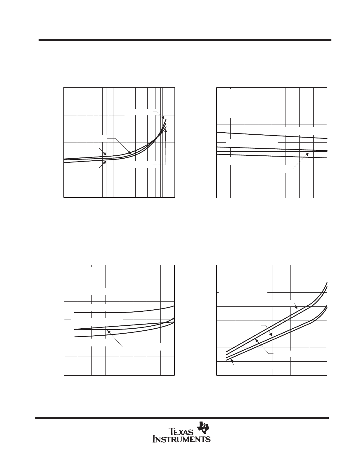
temperature (TA), and transverse airflow (FPM). Figures 6 (a) and 6 (b) show the relationship between ambient
temperature and transverse airflow at given power dissipation levels. The required transverse airflow can be
determined at a particular ambient temperature and device power dissipation level in order to ensure the device
specifications.
Figure 7 illustrates how power dissipation varies as a function of frequency and the number of outputs switching
simultaneously . It should be noted that all outputs are fully loaded (C
= 50 pF). Since the condition of eight fully
L
loaded outputs represents the worst-case condition, each application must be evaluated accordingly.
1000
800
600
400
MINIMUM TRANSVERSE AIR FLOW
vs
AMBIENT TEMPERATURE
PD = 1.6 W
PD = 1.4 W
PD = 1.2 W
PD = 1 W
PD = 0.8 W
PD = 0.6 W
1000
800
600
400
MINIMUM TRANSVERSE AIR FLOW
vs
AMBIENT TEMPERATURE
PD = 1.6 W
PD = 1.4 W
PD = 1.2 W
PD = 1 W
PD = 0.8 W
PD = 0.6 W
200
Minimum Transverse Air Flow – ft/min
0
30
4020100
TA – Ambient Temperature –°C
(a) TIBPAL16R8-5CN
60 70
8050
Figure 6
200
Minimum Transverse Air Flow – ft/min
0
30
4020100
TA – Ambient Temperature –°C
(b) TIBPAL16R8-5CFN
60 70
8050
20
POST OFFICE BOX 655303 • DALLAS, TEXAS 75265

THERMAL INFORMATION
POWER DISSIPATION
1800
VCC = 5 V
TA = 25 °C
CL = 50 pF
1600
8 Outputs Switching
1400
1200
1000
– Power Dissipation – mW
D
P
800
7 Outputs Switching
6 Outputs Switching
5 Outputs Switching
4 Outputs Switching
3 Outputs Switching
2 Outputs Switching
1 Output Switching
TIBPAL16R8-5C
HIGH-PERFORMANCE IMPACT-X PAL
SRPS011D – D3359, OCTOBER 1989 – REVISED SEPTEMBER 1992
vs
FREQUENCY
CIRCUITS
600
1 4 10 40 100
2 20 200
f – Frequency – MHz
Figure 7
POST OFFICE BOX 655303 • DALLAS, TEXAS 75265
21

TIBPAL16L8-5C, TIBPAL16R4-5C, TIBPAL16R6-5C, TIBPAL16R8-5C
TIBPAL16L8-7M, TIBPAL16R4-7M, TIBPAL16R6-7M, TIBPAL16R8-7M
HIGH-PERFORMANCE IMPACT-X PAL
SRPS011D – D3359, OCTOBER 1989 – REVISED SEPTEMBER 1992
PARAMETER MEASUREMENT INFORMATION
From Output
Under Test
CIRCUITS
5 V
S1
R1
Test
Point
Timing
Input
Data
Input
Input
In-Phase
Output
Out-of-Phase
Output
(see Note D)
1.5 V
t
su
1.5 V
VOLTAGE WAVEFORMS
SETUP AND HOLD TIMES
1.5 V 1.5 V
t
pd
80 %
20 %
t
pd
20 %
80 %
VOLTAGE WAVEFORMS
PROPAGATION DELAY TIMES
1.5 V
1.5 V 1.5 V
1.5 V
t
r
t
f
(see Note A)
t
h
t
pd
1.5 V
t
t
pd
t
C
L
3 V
0
3 V
0
(see Note B)
3 V
0
V
OH
V
OL
f
V
OH
V
OL
r
R2
LOAD CIRCUIT FOR
3-STATE OUTPUTS
High-Level
Low-Level
Output
Control
(low-level
enabling)
Waveform 1
S1 Closed
(see Note C)
Waveform 2
S1 Open
(see Note C)
Pulse
Pulse
VOLTAGE WAVEFORMS
PULSE DURATIONS
1.5 V 1.5 V
t
en
t
en
1.5 V 1.5 V
t
w
1.5 V 1.5 V
t
dis
1.5 V
t
dis
1.5 V
3 V
0
3 V
0
(see Note B)
3 V
0
(see Note B)
≈ 2.7 V
V
OL
VOL + 0.5 V
V
OH
VOH – 0.5 V
≈ 0 V
ENABLE AND DISABLE TIMES, 3-STATE OUTPUTS
NOTES: A. CL includes probe and jig capacitance and is 50 pF for tpd and ten, 5 pF for t
B. All input pulses have the following characteristics: For C suffix, PRR ≤ 1 MHz, tr = tf = 2 ns, duty cycle = 50%; For M suffix,
PRR ≤ 10 MHz, tr = tf ≤ 2 ns, duty cycle = 50%
C. Waveform 1 is for an output with internal conditions such that the output is low except when disabled by the output control. W aveform 2
is for an output with internal conditions such that the output is high except when disabled by the output control.
D. When measuring propagation delay times of 3-state outputs, switch S1 is closed.
E. Equivalent loads may be used for testing.
Figure 8. Load Circuit and Voltage Waveforms
22
POST OFFICE BOX 655303 • DALLAS, TEXAS 75265
VOLTAGE WAVEFORMS
.
dis
TIBPAL16R4-5C, TIBPAL16R6-5C, TIBPAL16R8-5C
C1
CIRCUITS
HIGH-PERFORMANCE IMPACT -X PAL
SRPS011D – D3359, OCTOBER 1989 – REVISED SEPTEMBER 1992
metastable characteristics of TIBPAL16R4-5C, TIBPAL16R6-5C, and TIBPAL16R8-5C
At some point a system designer is faced with the problem of synchronizing two digital signals operating at two
different frequencies. This problem is typically overcome by synchronizing one of the signals to the local clock
through use of a flip-flop. However, this solution presents an awkward dilemma since the setup and hold time
specifications associated with the flip-flop are sure to be violated. The metastable characteristics of the flip-flop
can influence overall system reliability.
Whenever the setup and hold times of a flip-flop are violated, its output response becomes uncertain and is said
to be in the metastable state if the output hangs up in the region between V
lasts until the flip-flop falls into one of its two stable states, which takes longer than the specified maximum
propagation delay time (CLK to Q max).
From a system engineering standpoint, a designer cannot use the specified data sheet maximum for
propagation delay time when using the flip-flop as a data synchronizer – how long to wait after the specified data
sheet maximum must be known before using the data in order to guarantee reliable system operation.
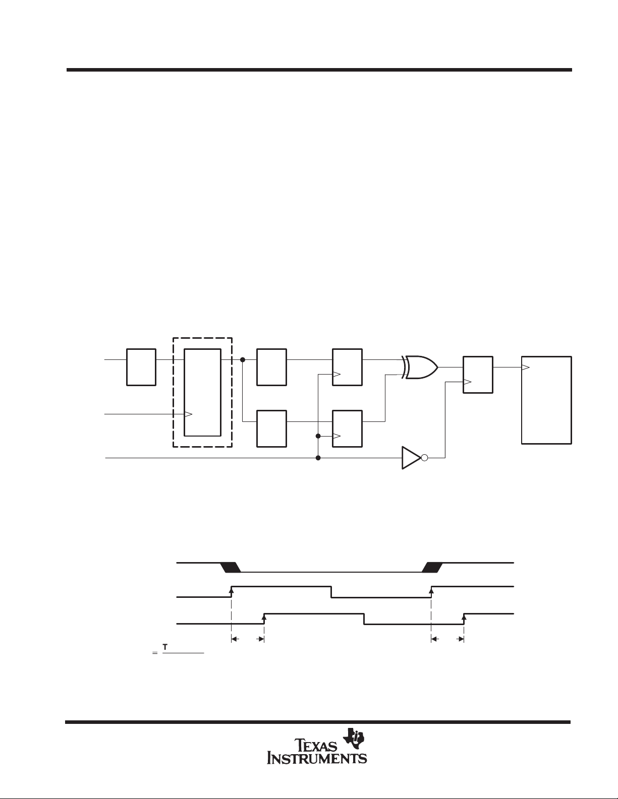
The circuit shown in Figure 9 can be used to evaluate MTBF (Mean Time Between Failure) and ∆t for a selected
flip-flop. Whenever the Q output of the DUT is between 0.8 V and 2 V , the comparators are in opposite states.
When the Q output of the DUT is higher than 2 V or lower than 0.8 V , the comparators are at the same logic level.
The outputs of the two comparators are sampled a selected time (∆t) after system clock (SCLK). The exclusive
OR gate detects the occurrence of a failure and increments the failure counter.
1D
DUT
C1
V
IH
Comparator
V
IL
Comparator
1D
C1
1D
C1
Noise
Generator
Data in
SCLK
and VIH. This metastable condition
IL
1D
MTBF
Counter
+
SCLK + ∆t
Figure 9. Metastable Evaluation Test Circuit
In order to maximize the possibility of forcing the DUT into a metastable state, the input data signal is applied
so that it always violates the setup and hold time. This condition is illustrated in the timing diagram in Figure 10.
Any other relationship of SCLK to data will provide less chance for the device to enter into the metastable state.
Data in
SCLK
SCLK + ∆t
MTBF
t
rec
Time (sec)
+
# Failures
= ∆t – CLK to Q (max)
∆t
∆t
Figure 10. Timing Diagram
POST OFFICE BOX 655303 • DALLAS, TEXAS 75265
23

TIBPAL16R4-5C, TIBPAL16R6-5C, TIBPAL16R8-5C
HIGH-PERFORMANCE IMPACT -X PAL
SRPS011D – D3359, OCTOBER 1989 – REVISED SEPTEMBER 1992
By using the described test circuit, MTBF can be determined for several different values of ∆t (see Figure 9).
Plotting this information on semilog scale demonstrates the metastable characteristics of the selected flip-flop.
Figure 11 shows the results for the TIBPAL16’-5C operating at 1 MHz.
9
10
10
10
10
10
10
10
10
10
MTBF – Mean Time Between Failures – s
10 yr
8
1 yr
7
1 mo
6
1 wk
5
1 day
4
1 hr
3
2
1 min
10 s
1
0 10203040506070
CIRCUITS
f
= 1 MHz
clk
f
data
∆t – Time Difference – ns
= 500 kHz
Figure 11. Metastable Characteristics
From the data taken in the above experiment, an equation can be derived for the metastable characteristics at
other clock frequencies.
The metastable equation:
1
MTBF
+
f
SCLK
xf
data
xC1e
(*C2 xDt)
The constants C1 and C2 describe the metastable characteristics of the device. From the experimental data,
these constants can be solved for: C1 = 4.37 X 10⁻³ and C2 = 2.01
Therefore
MTBF
1
+
f
SCLK
xf
x4.37x10
data
*
3e(*2.01 xDt)
definition of variables
DUT (Device Under Test): The DUT is a 5-ns registered PLD programmed with the equation Q : = D.
MTBF (Mean Time Between Failures): The average time (s) between metastable occurrences that cause a
violation of the device specifications.
f
(system clock frequency): Actual clock frequency for the DUT.
SCLK
f
(data frequency): Actual data frequency for a specified input to the DUT.
data
C1: Calculated constant that defines the magnitude of the curve.
C2: Calculated constant that defines the slope of the curve.
t
(metastability recovery time): Minimum time required to guarantee recovery from metastability , at a given
rec
MTBF failure rate. t
∆t: The time difference (ns) from when the synchronizing flip-flop is clocked to when its output is sampled.
= ∆t – tpd (CLK to Q, max)
rec
The test described above has shown the metastable characteristics of the TIBP AL16R4/R6/R8-5C series. For
additional information on metastable characteristics of Texas Instruments logic circuits, please refer to TI
Applications publication SDAA004, ”Metastable Characteristics, Design Considerations for ALS, AS, and LS
Circuits.’’
24
POST OFFICE BOX 655303 • DALLAS, TEXAS 75265

TIBPAL16L8-5C, TIBPAL16R4-5C, TIBPAL16R6-5C, TIBPAL16R8-5C
TIBPAL16L8-7M, TIBPAL16R4-7M, TIBPAL16R6-7M, TIBPAL16R8-7M
HIGH-PERFORMANCE IMPACT-X PAL
SRPS011D – D3359, OCTOBER 1989 – REVISED SEPTEMBER 1992
TYPICAL CHARACTERISTICS
CIRCUITS
LOW-LEVEL OUTPUT CURRENT
vs
LOW-LEVEL OUTPUT VOLTAGE
20
VCC = 5 V,
TA = 25 °C
15
10
5
0
–5
–10
– Low-Level Output Current – mA
OL
I
–15
–20
–0.8 –0.6 –0.4 –0.2 0 0.2
VOL – Low-Level Output Voltage – V
Figure 12
0.4 0.6 0.8
HIGH-LEVEL OUTPUT CURRENT
vs
HIGH-LEVEL OUTPUT VOLTAGE
0
VCC = 5 V,
–10
TA = 25 °C
–20
–30
–40
–50
–60
–70
– High-Level Output Current – mA
–80
OH
I
–90
–100
0 0.5 1 1.5 2 2.5
VOH – High-Level Output Voltage – V
Figure 13
3
SUPPLY CURRENT
FREE-AIR TEMPERATURE
220
200
180
160
140
– Supply Current – mA
CC
I
120
100
–75 –50 –25 0 25 50
TA – Free-Air Temperature – °C
Figure 14
vs
VCC = 5.5 V
VCC = 5.25 V
VCC = 4.5 V
VCC = 4.75 V
VCC = 5 V
75 100 125
POST OFFICE BOX 655303 • DALLAS, TEXAS 75265
25
TIBPAL16L8-5C, TIBPAL16R4-5C, TIBPAL16R6-5C, TIBPAL16R8-5C
TIBPAL16L8-7M, TIBPAL16R4-7M, TIBPAL16R6-7M, TIBPAL16R8-7M
HIGH-PERFORMANCE IMPACT-X PAL
SRPS011D – D3359, OCTOBER 1989 – REVISED SEPTEMBER 1992
TYPICAL CHARACTERISTICS
POWER DISSIPATION
vs
FREQUENCY
8-BIT COUNTER MODE
1100
VCC = 5 V
1000
TA = 80 °C
CIRCUITS
PROPAGATION DELAY TIME
6
TA = 25 °C
CL = 50 pF
R1 = 200 Ω
5
R2 = 200 Ω
1 Output Switching
SUPPLY VOLTAGE
vs
900
– Power Dissipation – mW
D
800
P
700
TA = 25 °C
TA = 0 °C
TA = 80 °C
2 20 200
1 4 10 40 100
f – Frequency – MHz
Figure 15
PROPAGATION DELAY TIME
vs
FREE-AIR TEMPERATURE
6
VCC = 5 V
CL = 50 pF
R1 = 200 Ω
5
R2 = 200 Ω
1 Output Switching
TA = 0 °C
4
t
3
2
Propagation Delay Time – ns
1
0
PLH
t
(CLK to Q)
PLH
4.5 4.75 5
PROPAGATION DELAY TIME
16
VCC = 5 V
TA = 25 °C
14
R1 = 200 Ω
R2 = 200 Ω
1 Output Switching
12
t
(I, I/O to O, I/O)
PHL
(I, I/O to O, I/O)
t
(CLK to Q)
PHL
VCC – Supply Voltage – V
Figure 16
vs
LOAD CAPACITANCE
5.25 5.5
26
4
t
(I, I/O to O, I/O)
PHL
3
t
(I, I/O to O, I/O)
PLH
2
t
(CLK to Q)
PLH
Propagation Delay Time – ns
1
0
–75 –50 –25 0 25 50
TA – Free-Air Temperature – °C
Figure 17
t
(CLK to Q)
PHL
75 100 125
POST OFFICE BOX 655303 • DALLAS, TEXAS 75265
t
(I, I/O to O, I/O)
10
8
t
PHL
6
4
Propagation Delay Time – ns
2
0
0 600
PHL
(CLK to Q)
t
(I, I/O to O, I/O)
PLH
t
(CLK to Q)
PLH
100 200 300 400
CL – Load Capacitance – pF
Figure 18
500
TIBPAL16L8-5C, TIBPAL16R4-5C, TIBPAL16R6-5C, TIBPAL16R8-5C
TIBPAL16L8-7M, TIBPAL16R4-7M, TIBPAL16R6-7M, TIBPAL16R8-7M
HIGH-PERFORMANCE IMPACT-X PAL
SRPS011D – D3359, OCTOBER 1989 – REVISED SEPTEMBER 1992
TYPICAL CHARACTERISTICS
CIRCUITS
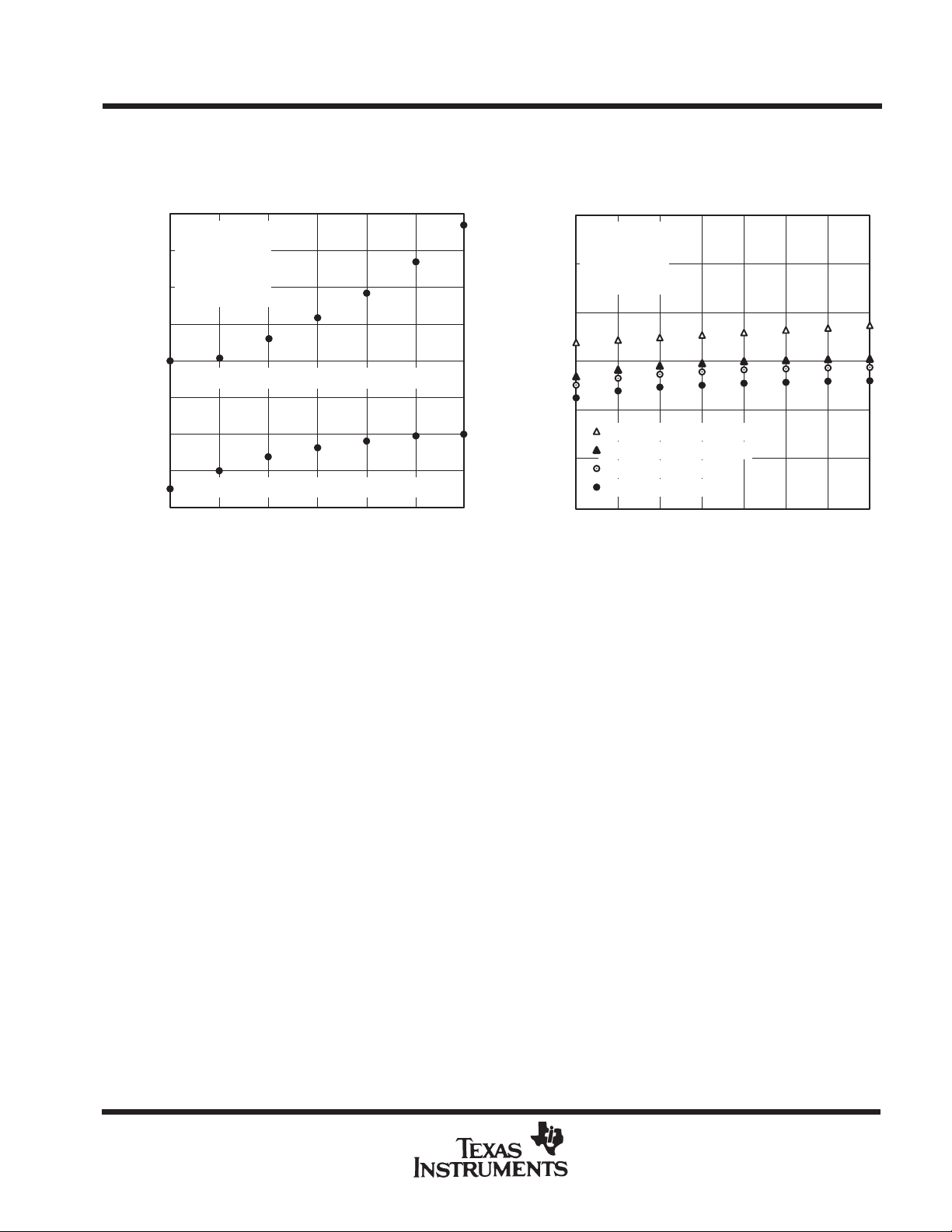
SKEW BETWEEN OUTPUTS
vs
NUMBER OF OUTPUTS SWITCHING
0.8
VCC = 5 V
TA = 25 °C
0.7
R1 = 200 Ω
R2 = 200 Ω
CL = 50 pF
0.6
8-Bit Counter
0.5
0.4
Outputs Switching in the Opposite Direction
0.3
0.2
– Skew Between Outputs Switching – ns
0.1
sk(o)
t
0
Outputs Switching in the Same Direction
23 4 56
Number of Outputs Switching
Figure 19
78
PROPAGATION DELAY TIME
NUMBER OF OUTPUTS SWITCHING
6
VCC = 5 V
TA = 25 °C
CL = 50 pF
5
R1 = 200 Ω
R2 = 200 Ω
4
3
2
= t
(I, I/O to O, I/O)
Propagation Delay Time – ns
1
0
12345
PHL
= t
(I, I/O to O, I/O)
PLH
= t
(CLK to Q)
PHL
= t
(CLK to Q)
PLH
Number of Outputs Switching
Figure 20
vs
678
POST OFFICE BOX 655303 • DALLAS, TEXAS 75265
27

TI North
American Sales
Offices
ALABAMA: Huntsville: (205) 837-7530
ARIZONA: Phoenix: (602) 995-1007
CALIFORNIA: Irvine: (714) 660-1200
San Diego: (619) 278-9600
Santa Clara: (408) 980-9000
Woodland Hills: (818) 704-8100
COLORADO: Aurora: (303) 368-8000
CONNECTICUT: W allingford: (203) 269-0074
FLORIDA: Altamonte Springs: (407) 260-2116
Fort Lauderdale: (305) 973-8502
Tampa: (813) 885-7588
GEORGIA: Norcross: (404) 662-7967
ILLINOIS: Arlington Heights: (708) 640-3000
INDIANA: Carmel: (317) 573-6400
Fort Wayne: (219) 489-4697
KANSAS: Overland Park: (913) 451-4511
MARYLAND: Columbia: (410) 964-2003
MASSACHUSETTS: Waltham: (617) 895-9100
MICHIGAN: Farmington Hills: (313) 553-1581
MINNESOTA: Eden Prairie: (612) 828-9300
MISSOURI: St. Louis: (314) 821-8400
NEW JERSEY: Iselin: (908) 750-1050
NEW MEXICO: Albuquerque: (505) 345-2555
NEW YORK: East Syracuse: (315) 463-9291
Fishkill: (914) 897-2900
Melville: (516) 454-6600
Pittsford: (716) 385-6770
NORTH CAROLINA: Charlotte: (704) 527-0930
Raleigh: (919) 876-2725
OHIO: Beachwood: (216) 765-7258
Beavercreek: (513) 427-6200
OREGON: Beaverton: (503) 643-6758
PENNSYLVANIA: Blue Bell: (215) 825-9500
PUERTO RICO: Hato Rey: (809) 753-8700
TEXAS: Austin: (512) 250-6769
Dallas: (214) 917-1264
Houston: (713) 778-6592
Midland: (915) 561-7137
UTAH: Salt Lake CIty: (801) 466-8972
WISCONSIN: Waukesha: (414) 798-1001
CANADA: Nepean: (613) 726-1970
Richmond Hill: (416) 884-9181
St. Laurent: (514) 335-8392
TI Regional
Technology
Centers
CALIFORNIA: Irvine: (714) 660-8140
Santa Clara: (408) 748-2222
GEORGIA: Norcross: (404) 662-7945
ILLINOIS: Arlington Heights: (708) 640-2909
INDIANA: Indianapolis: (317) 573-6400
MASSACHUSETTS: Waltham: (617) 895-9196
MEXICO: Mexico City: 491-70834
MINNESOTA: Minneapolis: (612) 828-9300
TEXAS: Dallas: (214) 917-3881
CANADA: Nepean: (613) 726-1970
TI Authorized
North American
Distributors
Alliance Electronics, Inc. (military product only)
Almac/Arrow
Anthem Electronics
Arrow/Schweber
Future Electronics (Canada)
GRS Electronics Co., Inc.
Hall-Mark Electronics
Marshall Industries
Newark Electronics
Rochester Electronics, Inc.
(obsolete product only (508) 462-9332)
Wyle Laboratories
Zeus Components
TI Distributors
ALABAMA: Arrow/Schweber (205) 837-6955; Hall-Mark
(205) 837-8700; Marshall (205) 881-9235.
ARIZONA: Anthem (602) 966-6600; Arrow/Schweber (602)
437-0750; Hall-Mark (602) 431-0030; Marshall (602)
496-0290; Wyle (602) 437-2088.
CALIFORNIA: Los Angeles/Orange County: Anthem
(818) 775-1333, (714) 768-4444; Arrow/Schweber (818)
380-9686, (714) 838-5422; Hall-Mark (818) 773-4500, (714)
727-6000; Marshall (818) 878-7000, (714) 458-5301; Wyle
(818) 880-9000, (714) 863-9953; Zeus (714) 921-9000,
(818) 889-3838;
Sacramento: Anthem (916) 624-9744; Hall-Mark (916)
624-9781; Marshall (916) 635-9700; Wyle (916) 638-5282;
San Diego: Anthem (619) 453-9005; Arrow/Schweber
(619) 565-4800; Hall-Mark (619) 268-1201; Marshall (619)
578-9600; Wyle (619) 565-9171; Zeus (619) 277-9681.
San Francisco Bay Area: Anthem (408) 453-1200;
Arrow/Schweber (408) 441-9700, (510) 490-9477;
Hall-Mark (408) 432-4000; Marshall (408) 942-4600;
Wyle (408) 727-2500; Zeus (408) 629-4789.
COLORADO: Anthem (303) 790-4500; Arrow/Schweber
(303) 799-0258; Hall-Mark (303) 790-1662; Marshall (303)
451-8383; Wyle (303) 457-9953.
CONNECTICUT: Anthem (203) 575-1575; Arrow/Schweber
(203) 265-7741; Hall-Mark (203) 271-2844; Marshall (203)
265-3822.
FLORIDA:Fort Lauderdale:Arrow/Schweber (305)
429-8200; Halll-Mark (305) 971-9280; Marshall (305)
977-4880.
Orlando: Arrow/Schweber (407) 333-9300; Hall-Mark (407)
830-5855; Marshall (407) 767-8585; Zeus (407) 788-9100.
Tampa: Hall-Mark (813) 541-7440; Marshall (813)
573-1399.
GEORGIA: Arrow/Schweber (404) 497-1300; Hall-Mark
(404) 623-4400; Marshall (404) 923-5750.
ILLINOIS: Anthem (708) 884-0200; Arrow/Schweber (708)
250-0500; Hall-Mark (312) 860-3800; Marshall (708)
490-0155; Newark (312)784-5100.
INDIANA: Arrow/Schweber (317) 299-2071; Hall-Mark
(317) 872-8875; Marshall (317) 297-0483.
IOWA: Arrow/Schweber (319) 395-7230.
KANSAS: Arrow/Schweber (913) 541-9542; Hall-Mark
(913) 888-4747; Marshall (913) 492-3121.
MARYLAND: Anthem (301) 995-6640; Arrow/Schweber
(301) 596-7800; Hall-Mark (301) 988-9800; Marshall (301)
622-1118; Zeus (301) 997-1118.
MASSACHUSETTS: Anthem (508) 657-5170;
Arrow/Schweber (508) 658-0900; Hall-Mark (508)
667-0902; Marshall (508) 658-0810; Wyle (617) 272-7300;
Zeus (617) 246-8200.
MICHIGAN: Detroit: Arrow/Schweber (313) 462-2290;
Hall-Mark (313) 416-5800; Marshall (313) 525-5850;
Newark (313) 967-0600.
MINNESOTA: Anthem (612) 944-5454; Arrow/Schweber
(612) 941-5280; Hall-Mark (612) 881-2600; Marshall (612)
559-2211.
MISSOURI: Arrow/Schweber (314) 567-6888; Hall-Mark
(314) 291-5350; Marshall (314) 291-4650.
NEW JERSEY: Anthem (201) 227-7960; Arrow/Schweber
(201) 227-7880, (609) 596-8000; Hall-Mark (201) 515-3000,
(609) 235-1900; Marshall (201) 882-0320, (609) 234-9100.
NEW MEXICO: Alliance (505) 292-3360.
NEW YORK: Long Island: Anthem (516) 864-6600;
Arrow/Schweber (516) 231-1000; Hall-Mark (516)
737-0600; Marshall (516) 273-2424; Zeus (914) 937-7400.
Rochester: Arrow/Schweber (716) 427-0300; Hall-Mark
(716) 425-3300; Marshall (716) 235-7620.
Syracuse: Marshall (607) 785-2345.
NORTH CAROLINA: Arrow/Schweber (919) 876-3132;
Hall-Mark (919) 872-0712; Marshall (919) 878-9882.
OHIO: Cleveland: Arrow/Schweber (216) 248-3990;
Hall-Mark (216) 349-4632; Marshall (216) 248-1788.
Columbus: Hall-Mark (614) 888-3313.
Dayton: Arrow/Schweber (513) 435-5563; Marshall (513)
898-4480; Zeus (513) 293-6162.
OKLAHOMA: Arrow/Schweber (918) 252-7537; Hall-Mark
(918) 254-6110.
OREGON: Almac/Arrow (503) 629-8090; Anthem (503)
643-1114; Marshall (503) 644-5050; Wyle (503) 643-7900.
PENNSYLVANIA: Anthem (215) 443-5150;
Arrow/Schweber (215) 928-1800; GRS (215) 922-7037;
(609) 964-8560; Marshall (412) 788-0441.
TEXAS: Austin: Arrow/Schweber (512) 835-4180;
Hall-Mark (512) 258-8848; Marshall (512) 837-1991; Wyle
(512) 345-8853;
Dallas: Anthem (214) 238-7100; Arrow/Schweber (214)
380-6464; Hall-Mark (214) 553-4300; Marshall (214)
233-5200; Wyle (214) 235-9953; Zeus (214) 783-7010;
Houston: Arrow/Schweber (713) 530-4700; Hall-Mark
(713) 781-6100; Marshall (713) 467-1666; Wyle (713)
879-9953.
UTAH: Anthem (801) 973-8555; Arrow/Schweber (801)
973-6913; Marshall (801) 973-2288; Wyle (801) 974-9953.
WASHINGTON: Almac/Arrow (206) 643-9992, Anthem
(206) 483-1700; Marshall (206) 486-5747; Wyle (206)
881-1150.
WISCONSIN: Arrow/Schweber (414) 792-0150; Hall-Mark
(414) 797-7844; Marshall (414) 797-8400.
CANADA: Calgary: Future (403) 235-5325;
Edmonton: Future (403) 438-2858;
Montreal: Arrow/Schweber (514) 421-7411; Future (514)
694-7710; Marshall (514) 694-8142
Ottawa: Arrow/Schweber (613) 226-6903; Future (613)
820-8313.
Quebec: Future (418) 897-6666.
Toronto: Arrow/Schweber (416) 670-7769;
Future (416) 612-9200; Marshall (416) 458-8046.
Vancouver: Arrow/Schweber (604) 421-2333;
Future (604) 294-1166.
TI Die Processors
Chip Supply (407) 298-7100
Elmo Semiconductor (818) 768-7400
Minco T echnology Labs (512) 834-2022
Customer
Response Center
TOLL FREE: (800) 336-5236
OUTSIDE USA: (214) 995-6611
(8:00 a.m. – 5:00 p.m. CST)
1992 T exas Instruments Incorporated
D0892
SRPS011D
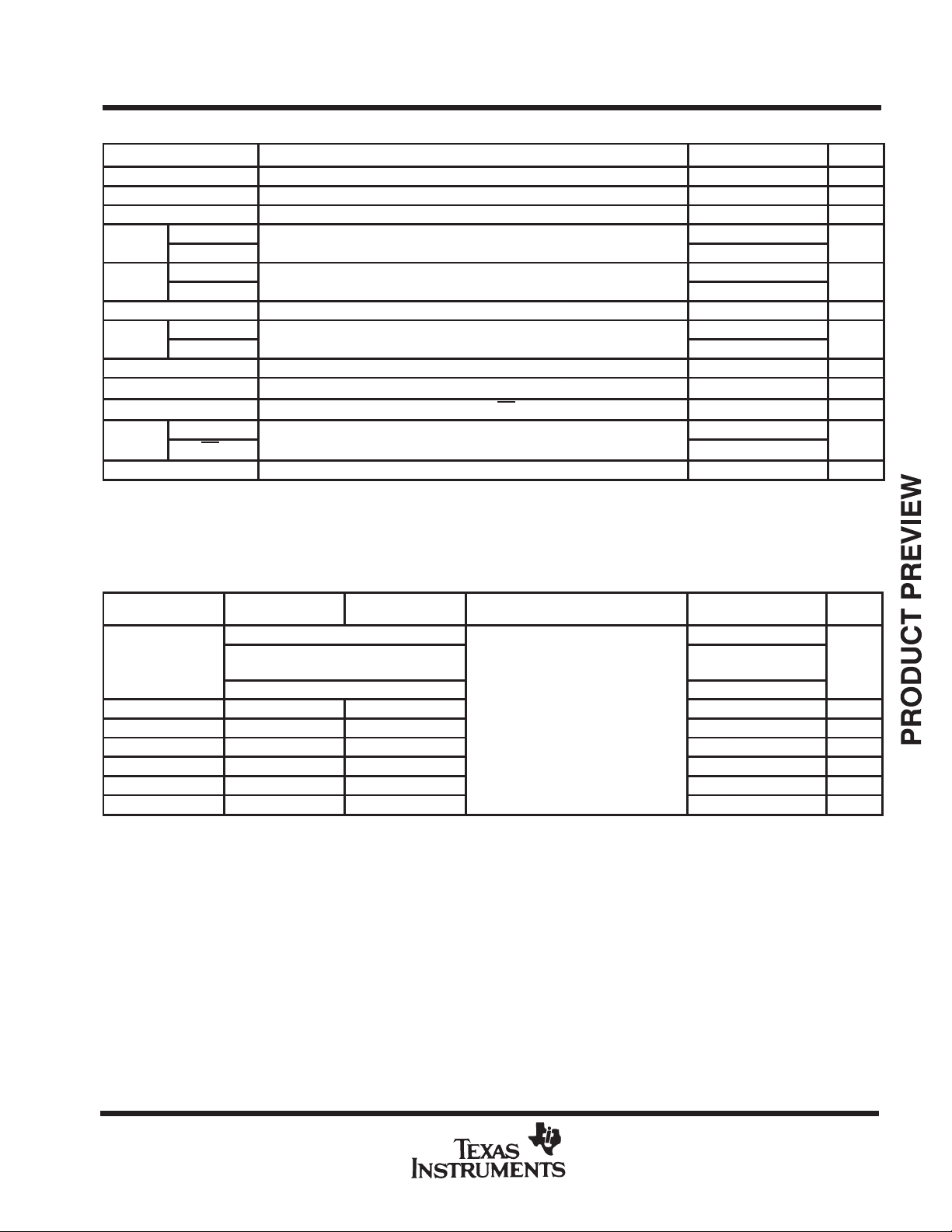
PACKAGE OPTION ADDENDUM
www.ti.com
4-Mar-2005
PACKAGING INFORMATION
Orderable Device Status
(1)
Package
Type
Package
Drawing
Pins Package
Qty
Eco Plan
5962-85155212A ACTIVE LCCC FK 20 1 None Call TI Level-NC-NC-NC
5962-8515521RA ACTIVE CDIP J 20 1 None Call TI Level-NC-NC-NC
5962-8515521SA ACTIVE CFP W 20 1 None Call TI Level-NC-NC-NC
5962-85155222A ACTIVE LCCC FK 20 1 None Call TI Level-NC-NC-NC
5962-8515522RA ACTIVE CDIP J 20 1 None Call TI Level-NC-NC-NC
5962-8515522SA ACTIVE CFP W 20 1 None Call TI Level-NC-NC-NC
TIBPAL16L8-5CFN OBSOLETE PLCC FN 20 None Call TI Call TI
TIBPAL16L8-5CN OBSOLETE PDIP N 20 None Call TI Call TI
TIBPAL16R4-5CFN ACTIVE PLCC FN 20 46 None Call TI Level-1-220-UNLIM
TIBPAL16R4-5CN NRND PDIP N 20 20 None Call TI Level-NC-NC-NC
TIBPAL16R4-7MFKB ACTIVE LCCC FK 20 1 None Call TI Level-NC-NC-NC
TIBPAL16R4-7MJB ACTIVE CDIP J 20 1 None Call TI Level-NC-NC-NC
TIBPAL16R4-7MWB ACTIVE CFP W 20 1 None Call TI Level-NC-NC-NC
TIBPAL16R6-5CFN ACTIVE PLCC FN 20 46 None Call TI Level-1-220-UNLIM
TIBPAL16R6-5CN ACTIVE PDIP N 20 20 None Call TI Level-NC-NC-NC
TIBPAL16R8-5CFN ACTIVE PLCC FN 20 46 None Call TI Level-1-220-UNLIM
TIBPAL16R8-5CN ACTIVE PDIP N 20 20 None Call TI Level-NC-NC-NC
TIBPAL16R8-7MFKB ACTIVE LCCC FK 20 1 None Call TI Level-NC-NC-NC
TIBPAL16R8-7MJB ACTIVE CDIP J 20 1 None Call TI Level-NC-NC-NC
TIBPAL16R8-7MWB ACTIVE CFP W 20 1 None Call TI Level-NC-NC-NC
(1)
The marketing status values are defined as follows:
ACTIVE: Product device recommended for new designs.
LIFEBUY: TI has announced that the device will be discontinued, and a lifetime-buy period is in effect.
NRND: Not recommended for new designs. Device is in production to support existing customers, but TI does not recommend using this part in
a new design.
PREVIEW: Device has been announced but is not in production. Samples may or may not be available.
OBSOLETE: TI has discontinued the production of the device.
(2)
Lead/Ball Finish MSL Peak Temp
(3)
(2)
Eco Plan - May not be currently available - please check http://www.ti.com/productcontent for the latest availability information and additional
product content details.
None: Not yet available Lead (Pb-Free).
Pb-Free (RoHS): TI's terms "Lead-Free" or "Pb-Free" mean semiconductor products that are compatible with the current RoHS requirements
for all 6 substances, including the requirement that lead not exceed 0.1% by weight in homogeneous materials. Where designed to be soldered
at high temperatures, TI Pb-Free products are suitable for use in specified lead-free processes.
Green (RoHS & no Sb/Br): TI defines "Green" to mean "Pb-Free" and in addition, uses package materials that do not contain halogens,
including bromine (Br) or antimony (Sb) above 0.1% of total product weight.
(3)
MSL, Peak Temp. -- The Moisture Sensitivity Level rating according to the JEDECindustry standard classifications, and peak solder
temperature.
Important Information and Disclaimer:The information provided on this page represents TI's knowledge and belief as of the date that it is
provided. TI bases its knowledge and belief on information provided by third parties, and makes no representation or warranty as to the
accuracy of such information. Efforts are underway to better integrate information from third parties. TI has taken and continues to take
reasonable steps to provide representative and accurate information but may not have conducted destructive testing or chemical analysis on
incoming materials and chemicals. TI and TI suppliers consider certain information to be proprietary, and thus CAS numbers and other limited
information may not be available for release.
In no event shall TI's liability arising out of such information exceed the total purchase price of the TI part(s) at issue in this document sold by TI
to Customer on an annual basis.
Addendum-Page 1

IMPORTANT NOTICE
Texas Instruments Incorporated and its subsidiaries (TI) reserve the right to make corrections, modifications,
enhancements, improvements, and other changes to its products and services at any time and to discontinue
any product or service without notice. Customers should obtain the latest relevant information before placing
orders and should verify that such information is current and complete. All products are sold subject to TI’s terms
and conditions of sale supplied at the time of order acknowledgment.
TI warrants performance of its hardware products to the specifications applicable at the time of sale in
accordance with TI’s standard warranty. Testing and other quality control techniques are used to the extent TI
deems necessary to support this warranty . Except where mandated by government requirements, testing of all
parameters of each product is not necessarily performed.
TI assumes no liability for applications assistance or customer product design. Customers are responsible for
their products and applications using TI components. To minimize the risks associated with customer products
and applications, customers should provide adequate design and operating safeguards.
TI does not warrant or represent that any license, either express or implied, is granted under any TI patent right,
copyright, mask work right, or other TI intellectual property right relating to any combination, machine, or process
in which TI products or services are used. Information published by TI regarding third-party products or services
does not constitute a license from TI to use such products or services or a warranty or endorsement thereof.
Use of such information may require a license from a third party under the patents or other intellectual property
of the third party, or a license from TI under the patents or other intellectual property of TI.
Reproduction of information in TI data books or data sheets is permissible only if reproduction is without
alteration and is accompanied by all associated warranties, conditions, limitations, and notices. Reproduction
of this information with alteration is an unfair and deceptive business practice. TI is not responsible or liable for
such altered documentation.
Resale of TI products or services with statements different from or beyond the parameters stated by TI for that
product or service voids all express and any implied warranties for the associated TI product or service and
is an unfair and deceptive business practice. TI is not responsible or liable for any such statements.
Following are URLs where you can obtain information on other Texas Instruments products and application
solutions:
Products Applications
Amplifiers amplifier.ti.com Audio www.ti.com/audio
Data Converters dataconverter.ti.com Automotive www.ti.com/automotive
DSP dsp.ti.com Broadband www.ti.com/broadband
Interface interface.ti.com Digital Control www.ti.com/digitalcontrol
Logic logic.ti.com Military www.ti.com/military
Power Mgmt power.ti.com Optical Networking www.ti.com/opticalnetwork
Microcontrollers microcontroller.ti.com Security www.ti.com/security
Telephony www.ti.com/telephony
Video & Imaging www.ti.com/video
Wireless www.ti.com/wireless
Mailing Address: Texas Instruments
Post Office Box 655303 Dallas, Texas 75265
Copyright 2005, Texas Instruments Incorporated
 Loading...