

TEXAS INSTRUMENTS TIBPAL16L8-15M, TIBPAL16R4-15M, TIBPAL16R6-15M, TIBPAL16R8-15M Technical data
查询TIBPAL16L8-15M供应商
TIBPAL16L8-15M, TIBPAL16R4-15M, TIBPAL16R6-15M, TIBPAL16R8-15M
HIGH-PERFORMANCE IMPACT PAL
SRPS018A – D3338, JANUARY 1986 – REVISED MAY 1996
CIRCUITS
D
High-Performance Operation:
Propagation Delay . . . 15 ns Max
D
Power-Up Clear on Registered Devices (All
Register Outputs are Set High, but Voltage
Levels at the Output Pins Go Low)
D
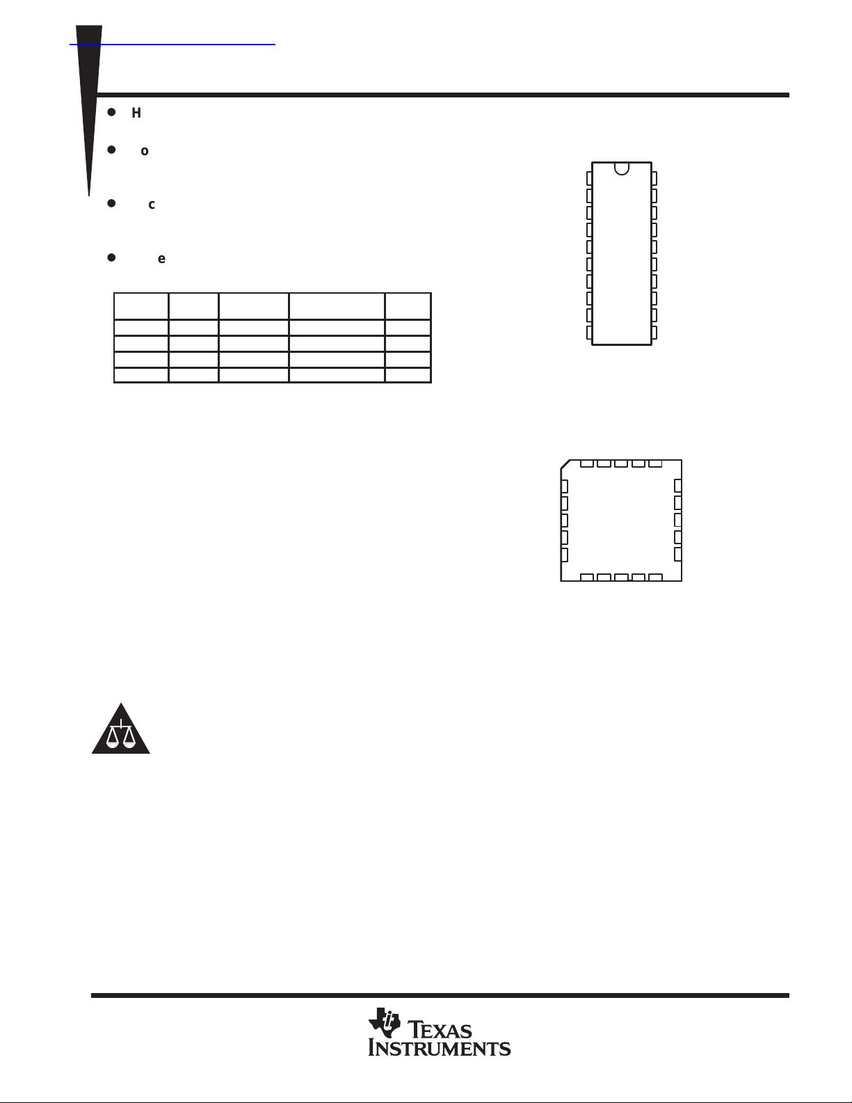
Package Options Include Ceramic Flat (W)
Packages, Ceramic Chip Carriers (FK), and
Ceramic (J) 300-mil DIPs
D
Dependable Texas Instruments Quality and
Reliability
DEVICE
PAL16L8 10 2 0 6
PAL16R4 8 0 4 (3-state buffers) 4
PAL16R6 8 0 6 (3-state buffers) 2
PAL16R8 8 0 8 (3-state buffers) 0
I
INPUTS
3-STATE
O OUTPUTS
REGISTERED
Q OUTPUTS
description
These programmable array logic devices feature
high speed and functional equivalency when
compared with currently available devices. These
IMP ACT-X circuits combine the latest Advanced
Low-Power Schottky technology with proven
titanium-tungsten fuses to provide reliable,
high-performance substitutes for conventional
TTL logic. Their easy programmability allows for
quick design of custom functions and typically
results in a more compact circuit board. In
addition, chip carriers are available for futher
reduction in board space.
The TIBPAL16’ M series is characterized for
operation over the full military temperature range
of –55°C to 125°C.
I/O
PORTS
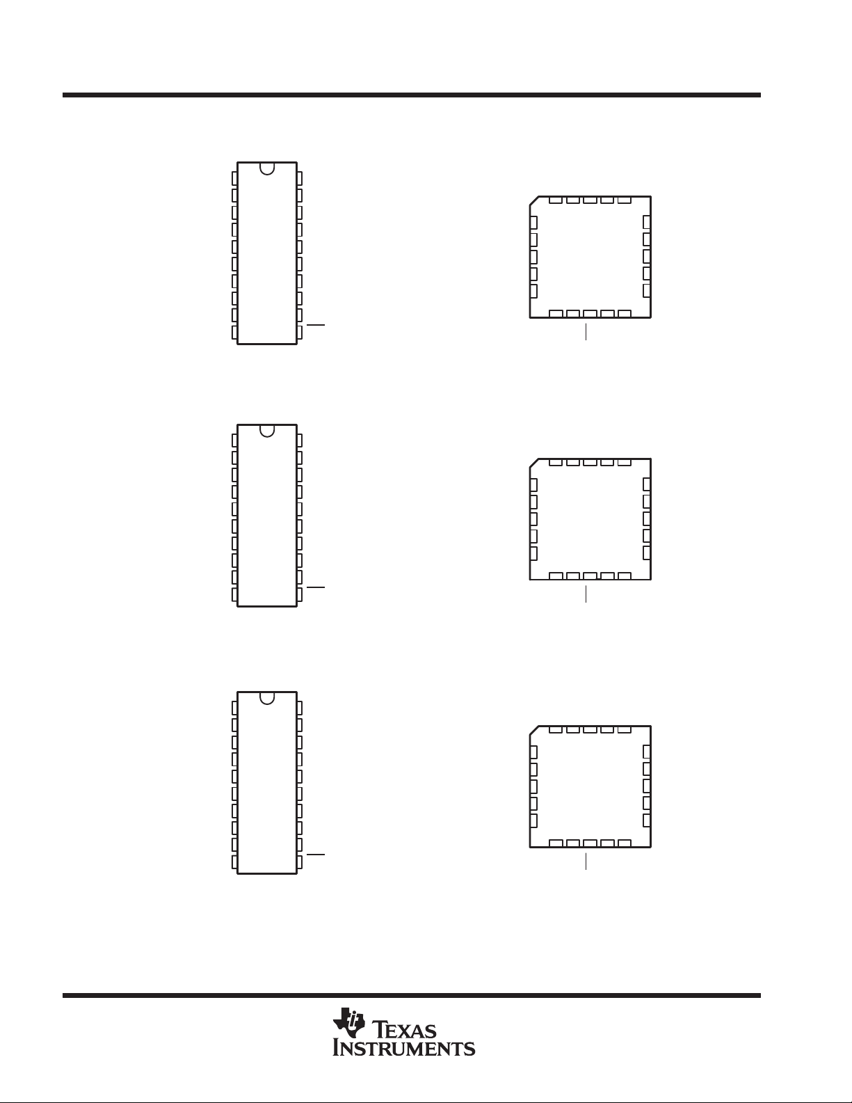
TIBPAL16L8’
J OR W PACKAGE
(TOP VIEW)
I
I
I
I
I
I
I
I
I
GND
FK PACKAGE
3 2 1 20 19
I
4
I
5
I
6
I
7
I
8
910111213
1
2
3
4
5
6
7
8
9
10
TIBPAL16L8’
(TOP VIEW)
I
I
I
V
20
CC
O
19
I/O
18
I/O
17
I/O
16
15
I/O
14
I/O
13
I/O
12
O
11
I
CC
I
O
V
I/O
18
I/O
17
I/O
16
I/O
15
I/O
14
I
O
I/O
GND
Pin assignments in operating mode
Please be aware that an important notice concerning availability, standard warranty, and use in critical applications of
Texas Instruments semiconductor products and disclaimers thereto appears at the end of this data sheet.
IMPACT is a trademark of Texas Instruments Incorporated.
PAL is a registered trademark of Advanced Micro Devices Inc.
PRODUCTION DATA information is current as of publication date.
Products conform to specifications per the terms of Texas Instruments
standard warranty. Production processing does not necessarily include
testing of all parameters.
POST OFFICE BOX 655303 • DALLAS, TEXAS 75265
Copyright 1996, Texas Instruments Incorporated
1
TIBPAL16L8-15M, TIBPAL16R4-15M, TIBPAL16R6-15M, TIBPAL16R8-15M
HIGH-PERFORMANCE IMPACT PAL
CIRCUITS
SRPS018A – D3338, JANUARY 1986 – REVISED MAY 1996
TIBPAL16R4’
J OR W PACKAGE
(TOP VIEW)
CLK
1
I
2
I
3
I
4
I
5
I
6
I
7
I
8
I
9
GND
GND
10
TIBPAL16R6’
J OR W PACKAGE
(TOP VIEW)
CLK
1
I
2
I
3
I
4
I
5
I
6
I
7
I
8
I
9
10
20
19
18
17
16
15
14
13
12
11
20
19
18
17
16
15
14
13
12
11
V
I/O
I/O
Q
Q
Q
Q
I/O
I/O
OE
V
I/O
Q
Q
Q
Q
Q
Q
I/O
OE
CC
CC
TIBPAL16R4’
FK PACKAGE
(TOP VIEW)
I
3212019
I
4
I
5
I
6
I
7
I
8
910111213
I
TIBPAL16R6’
FK PACKAGE
(TOP VIEW)
I
3212019
I
4
I
5
I
6
I
7
I
8
910111213
I
I
CLK
GND
I
CLK
GND
OE
OE
V
I/O
V
I/O
CC
CC
I/O
18
17
16
15
14
I/O
I/O
18
17
16
15
14
Q
I/O
Q
Q
Q
Q
Q
Q
Q
Q
Q
J OR W PACKAGE
CLK
I
I
I
I
I
I
I
I
GND
Pin assignments in operating mode
TIBPAL16R8’
(TOP VIEW)
20
1
19
2
18
3
17
4
16
5
15
6
14
7
13
8
12
9
11
10
V
Q
Q
Q
Q
Q
Q
Q
Q
OE
CC
TIBPAL16R8’
FK PACKAGE
(TOP VIEW)
I
3212019
I
4
I
5
I
6
I
7
I
8
910111213
I
I
CLK
GND
OE
V
Q
CC
Q
18
17
16
15
14
Q
Q
Q
Q
Q
Q
2
POST OFFICE BOX 655303 • DALLAS, TEXAS 75265
TIBPAL16L8-15M, TIBPAL16R4-15M, TIBPAL16R6-15M, TIBPAL16R8-15M
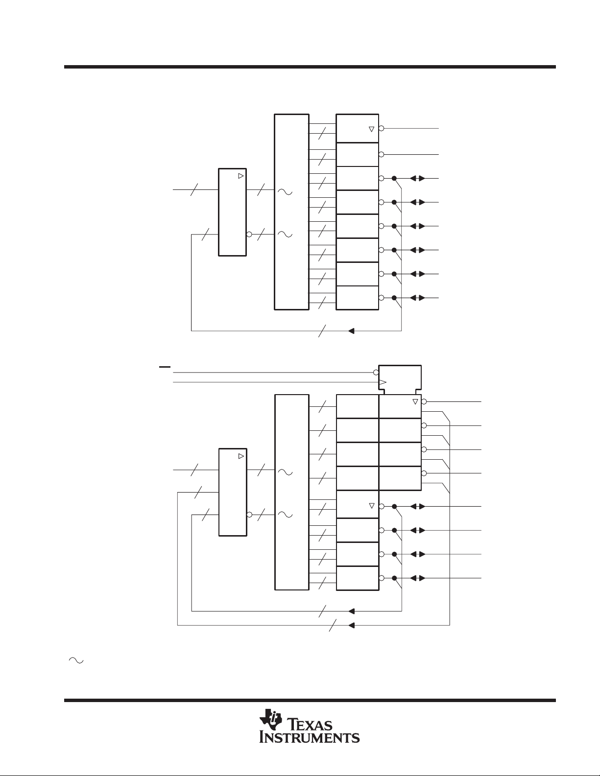
functional block diagrams (positive logic)
HIGH-PERFORMANCE IMPACT PAL
SRPS018A – D3338, JANUARY 1986 – REVISED MAY 1996
TIBPAL16L8’
CIRCUITS
OE
CLK
10 16
I
16 x
&
32 X 64
166
32 X 64
7
7
7
7
7
7
7
7
6
TIBPAL16R4 ’
&
8
8
EN
≥1
≥1
EN 2
C1
I = 1
1D
O
O
I/O
I/O
I/O
I/O
I/O
I/O
2
Q
Q
denotes fused inputs
816
I
16 x
4
164
8
8
≥1
EN
7
7
7
7
4
4
Q
Q
I/O
I/O
I/O
I/O
POST OFFICE BOX 655303 • DALLAS, TEXAS 75265
3
TIBPAL16L8-15M, TIBPAL16R4-15M, TIBPAL16R6-15M, TIBPAL16R8-15M
HIGH-PERFORMANCE IMPACT PAL
CIRCUITS
SRPS018A – D3338, JANUARY 1986 – REVISED MAY 1996
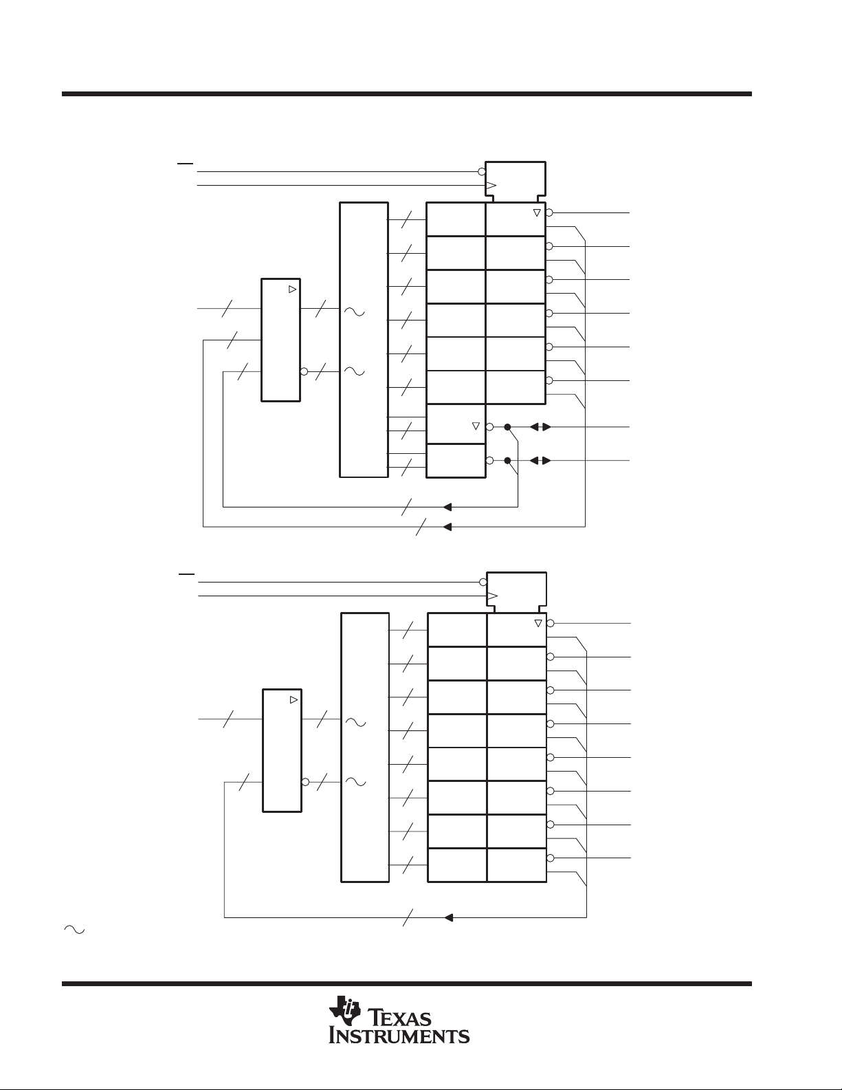
functional block diagrams (positive logic)
TIBPAL16R6’
OE
CLK
816
I
16 x
6
162
&
32 X 64
8
8
8
8
8
8
7
7
2
6
TIBPAL16R8 ’
EN
≥1
≥1
EN 2
C1
I = 1
1D
2
Q
Q
Q
Q
Q
Q
I/O
I/O
OE
CLK
denotes fused inputs
816
I
16 x
168
&
32 X 64
EN 2
C1
1D
I = 1
2
Q
Q
Q
Q
Q
Q
Q
Q
8
8
8
8
8
8
8
8
8
≥1
4
POST OFFICE BOX 655303 • DALLAS, TEXAS 75265
 Loading...