

Page 1

THS7002
ProgrammableĆGain Amplifier
Evaluation Module
User’s Guide
July 1999 Mixed-Signal Products
SLOU037
Page 2

IMPORTANT NOTICE
T exas Instruments and its subsidiaries (TI) reserve the right to make changes to their products or to discontinue
any product or service without notice, and advise customers to obtain the latest version of relevant information
to verify, before placing orders, that information being relied on is current and complete. All products are sold
subject to the terms and conditions of sale supplied at the time of order acknowledgement, including those
pertaining to warranty, patent infringement, and limitation of liability.
TI warrants performance of its semiconductor products to the specifications applicable at the time of sale in
accordance with TI’s standard warranty. Testing and other quality control techniques are utilized to the extent
TI deems necessary to support this warranty . Specific testing of all parameters of each device is not necessarily
performed, except those mandated by government requirements.
CERTAIN APPLICATIONS USING SEMICONDUCTOR PRODUCTS MAY INVOLVE POTENTIAL RISKS OF
DEATH, PERSONAL INJURY, OR SEVERE PROPERTY OR ENVIRONMENTAL DAMAGE (“CRITICAL
APPLICATIONS”). TI SEMICONDUCTOR PRODUCTS ARE NOT DESIGNED, AUTHORIZED, OR
WARRANTED TO BE SUITABLE FOR USE IN LIFE-SUPPORT DEVICES OR SYSTEMS OR OTHER
CRITICAL APPLICA TIONS. INCLUSION OF TI PRODUCTS IN SUCH APPLICATIONS IS UNDERST OOD TO
BE FULLY AT THE CUSTOMER’S RISK.
In order to minimize risks associated with the customer’s applications, adequate design and operating
safeguards must be provided by the customer to minimize inherent or procedural hazards.
TI assumes no liability for applications assistance or customer product design. TI does not warrant or represent
that any license, either express or implied, is granted under any patent right, copyright, mask work right, or other
intellectual property right of TI covering or relating to any combination, machine, or process in which such
semiconductor products or services might be or are used. TI’s publication of information regarding any third
party’s products or services does not constitute TI’s approval, warranty or endorsement thereof.
Copyright 1999, Texas Instruments Incorporated
Page 3

Related Documentation From Texas Instruments
J
THS7002 PROGRAMMABLE-GAIN AMPLIFIER
number SLOS214) This is the data sheet for the THS7002
amplifier integrated circuit used on the EVM.
J
THS4001 HIGH-SPEED LOW-POWER OPERATIONAL
AMPLIFIER
for the THS4001 amplifier integrated circuit used on the EVM.
J
PowerPAD Thermally Enhanced Package
SLMA002) This is the technical brief for the special PowerPAD
package in which the THS7002 amplifier IC is supplied.
(literature number SLOS206) This is the data sheet
FCC Warning
This equipment is intended for use in a laboratory test environment only. It
generates, uses, and can radiate radio frequency energy and has not been
tested for compliance with the limits of computing devices pursuant to subpart
J of part 15 of FCC rules, which are designed to provide reasonable protection
against radio frequency interference. Operation of this equipment in other
environments may cause interference with radio communications, in which
case the user at his own expense will be required to take whatever measures
may be required to correct this interference.
Preface
(literature
(literature number
Trademarks
TI is a trademark of Texas Instruments Incorporated.
PowerPAD is a trademark of Texas Instruments Incorporated.
Chapter Title—Attribute Reference
iii
Page 4

iv
Page 5

Running Title—Attribute Reference
Contents
1 General Information 1-1. . . . . . . . . . . . . . . . . . . . . . . . . . . . . . . . . . . . . . . . . . . . . . . . . . . . . . . . . . . . .
1.1 Features 1-2. . . . . . . . . . . . . . . . . . . . . . . . . . . . . . . . . . . . . . . . . . . . . . . . . . . . . . . . . . . . . . . . . .
1.2 Description 1-2. . . . . . . . . . . . . . . . . . . . . . . . . . . . . . . . . . . . . . . . . . . . . . . . . . . . . . . . . . . . . . . .
1.3 Programmable Gain Amplifier Gain Control 1-7. . . . . . . . . . . . . . . . . . . . . . . . . . . . . . . . . . . .
1.4 EVM DIP Switch Functionality 1-9. . . . . . . . . . . . . . . . . . . . . . . . . . . . . . . . . . . . . . . . . . . . . . . .
1.5 EVM Circuit Configuration 1-10. . . . . . . . . . . . . . . . . . . . . . . . . . . . . . . . . . . . . . . . . . . . . . . . . .
1.6 Using the THS7002 EVM 1-12. . . . . . . . . . . . . . . . . . . . . . . . . . . . . . . . . . . . . . . . . . . . . . . . . . .
1.7 THS7002 EVM Performance 1-13. . . . . . . . . . . . . . . . . . . . . . . . . . . . . . . . . . . . . . . . . . . . . . . .
1.8 General High-Speed Amplifier Design Considerations 1-16. . . . . . . . . . . . . . . . . . . . . . . . . .
1.9 General PowerP ADt Design Considerations 1-17. . . . . . . . . . . . . . . . . . . . . . . . . . . . . . . . . .
1.10 THS7002 EVM Specifications 1-20. . . . . . . . . . . . . . . . . . . . . . . . . . . . . . . . . . . . . . . . . . . . . . .
2 Reference 2-1. . . . . . . . . . . . . . . . . . . . . . . . . . . . . . . . . . . . . . . . . . . . . . . . . . . . . . . . . . . . . . . . . . . . . . .
2.1 THS7002 Programmable-Gain Amplifier EVM Parts List 2-2. . . . . . . . . . . . . . . . . . . . . . . . .
2.2 THS7002 EVM Board Layouts 2-3. . . . . . . . . . . . . . . . . . . . . . . . . . . . . . . . . . . . . . . . . . . . . . . .
Chapter Title—Attribute Reference
v
Page 6

Running Title—Attribute Reference
Figures
1–1 THS7002 Evaluation Module 1-3. . . . . . . . . . . . . . . . . . . . . . . . . . . . . . . . . . . . . . . . . . . . . . . . . . .
1–2 THS7002 EVM Power Conditioning Schematic Diagram 1-3. . . . . . . . . . . . . . . . . . . . . . . . . . . .
1–3 THS7002 EVM Schematic Diagram 1-4. . . . . . . . . . . . . . . . . . . . . . . . . . . . . . . . . . . . . . . . . . . . .
1–4 Simplified PGA Section of the THS7002 1-8. . . . . . . . . . . . . . . . . . . . . . . . . . . . . . . . . . . . . . . . . .
1–5 THS7002 Evaluation Module Block Diagram 1-10. . . . . . . . . . . . . . . . . . . . . . . . . . . . . . . . . . . . .
1–6 THS7002 EVM Preamplifier Frequency Response 1-13. . . . . . . . . . . . . . . . . . . . . . . . . . . . . . . .
1–7 THS7002 EVM Preamplifier Phase Response 1-13. . . . . . . . . . . . . . . . . . . . . . . . . . . . . . . . . . .
1–8 THS7002 EVM PGA Frequency Response 1-14. . . . . . . . . . . . . . . . . . . . . . . . . . . . . . . . . . . . . .
1–9 THS7002 EVM PGA Phase Response 1-14. . . . . . . . . . . . . . . . . . . . . . . . . . . . . . . . . . . . . . . . . .
1–10 THS7002 EVM Preamplifier + PGA Frequency Response 1-15. . . . . . . . . . . . . . . . . . . . . . . . .
1–11 THS7002 EVM Preamplifier + PGA Phase Response 1-15. . . . . . . . . . . . . . . . . . . . . . . . . . . . .
1–12 PowerPAD PCB Etch and Via Pattern 1-17. . . . . . . . . . . . . . . . . . . . . . . . . . . . . . . . . . . . . . . . . . .
1–13 Maximum Power Dissipation vs Free-Air Temperature 1-18. . . . . . . . . . . . . . . . . . . . . . . . . . . .
2–1 THS7002 EVM Component Placement Silkscreen and Solder Pads 2-3. . . . . . . . . . . . . . . . .
2–2 THS7002 EVM PC Board: Top Assembly 2-4. . . . . . . . . . . . . . . . . . . . . . . . . . . . . . . . . . . . . . . . .
2–3 THS7002 EVM PC Board: Top Layer 2-4. . . . . . . . . . . . . . . . . . . . . . . . . . . . . . . . . . . . . . . . . . . .
2–4 THS7002 EVM PC Board: Bottom Layer 2-5. . . . . . . . . . . . . . . . . . . . . . . . . . . . . . . . . . . . . . . . .
T ables
1–1 THS7002 EVM PGA Nominal Gain/Attenuation 1-7. . . . . . . . . . . . . . . . . . . . . . . . . . . . . . . . . . .
1–2 EVM DIP Switch Functionality 1-9. . . . . . . . . . . . . . . . . . . . . . . . . . . . . . . . . . . . . . . . . . . . . . . . . .
1–3 THS7002 EVM Jumper Settings 1-12. . . . . . . . . . . . . . . . . . . . . . . . . . . . . . . . . . . . . . . . . . . . . . .
1–4 THS7002 EVM DIP Switch Settings 1-12. . . . . . . . . . . . . . . . . . . . . . . . . . . . . . . . . . . . . . . . . . . .
2–1 THS7002 Programmable-Gain Amplifier EVM Parts List 2-2. . . . . . . . . . . . . . . . . . . . . . . . . . . .
vi
Page 7

Chapter 1
General
Information
This chapter details the Texas Instruments (TI) THS7002
programmable-gain amplifier evaluation module (EVM), SLOP136. It includes
a list of EVM features, a brief description of the module illustrated with pictorial
and schematic diagrams, EVM specifications, details on configuring,
connecting, and using the EVM, and a discussion on high-speed amplifier and
PowerPAD package design considerations.
Topic Page
1.1 Features 1–2. . . . . . . . . . . . . . . . . . . . . . . . . . . . . . . . . . . . . . . . . . . . . . . . . . . . .
1.2 Description 1–2. . . . . . . . . . . . . . . . . . . . . . . . . . . . . . . . . . . . . . . . . . . . . . . . . . .
1.3 Programmable Gain Amplifier Gain Control 1–7. . . . . . . . . . . . . . . . . . . . .
1.4 EVM DIP Switch Functionality 1–9. . . . . . . . . . . . . . . . . . . . . . . . . . . . . . . . . .
1.5 EVM CIrcuit Configuration 1–10. . . . . . . . . . . . . . . . . . . . . . . . . . . . . . . . . . .
1.6 Using The THS7002 EVM 1–12. . . . . . . . . . . . . . . . . . . . . . . . . . . . . . . . . . . .
1.7 THS7002 EVM Performance 1–13. . . . . . . . . . . . . . . . . . . . . . . . . . . . . . . . . .
1.8 General High-Speed Amplifier Design Considerations 1–16. . . . . . . . .
1.9 General PowerPAD Design Considerations 1–17. . . . . . . . . . . . . . . . . .
1.10 THS7002 EVM Specifications 1–20. . . . . . . . . . . . . . . . . . . . . . . . . . . . . . . . .
General Information
1-1
Page 8

Features
1.1 Features
1.2 Description
THS7002 programmable-gain amplifier EVM features include:
J
Multiple Input Configurations Set Via On-board Jumpers
J
DIP Switches Allow Quick and Easy Adjustment of Gain, Shut Down,
Reference Voltage, and Output Clamping
J
Includes a THS4001 High-Speed Amplifier as an Inverter
J
Standard BNC Connectors Inputs and Outputs
J
±5-V to ±15-V Operation with 5-V Reference Input
J
Nominal 50-Ω Impedance Inputs and Outputs
J
Includes T est Points for Easy Digital Control of EVM Circuit Gain and
Operating Parameters
J
Good Example of PowerPAD Package and High-Speed Amplifier
Design and Layout
The TI THS7002 programmable-gain amplifier evaluation module (EVM) is a
complete dual-channel low-noise receiver and a highly configurable
programmable-gain amplifier circuit. It consists of the TI THS7002
Programmable-Gain Amplifier IC, a TI THS4001 high-speed, low-power
operational amplifier IC, and a number of passive parts, all mounted on a
multilayer circuit board (Figure 1–1).
Although the THS7002 IC was developed primarily for xDSL receiver
front-ends, there are a large number of different circuits that can benefit from
the many features incorporated into the THS7002. This EVM illustrates a
universal design and can be used for numerous system configurations.
The EVM uses standard BNC connectors for inputs and outputs and also
includes test points for user connections and testing. It is completely
assembled, fully tested, and ready to use — just connect it to power, a signal
source, and a load (if desired).
1-2
General Information
Page 9
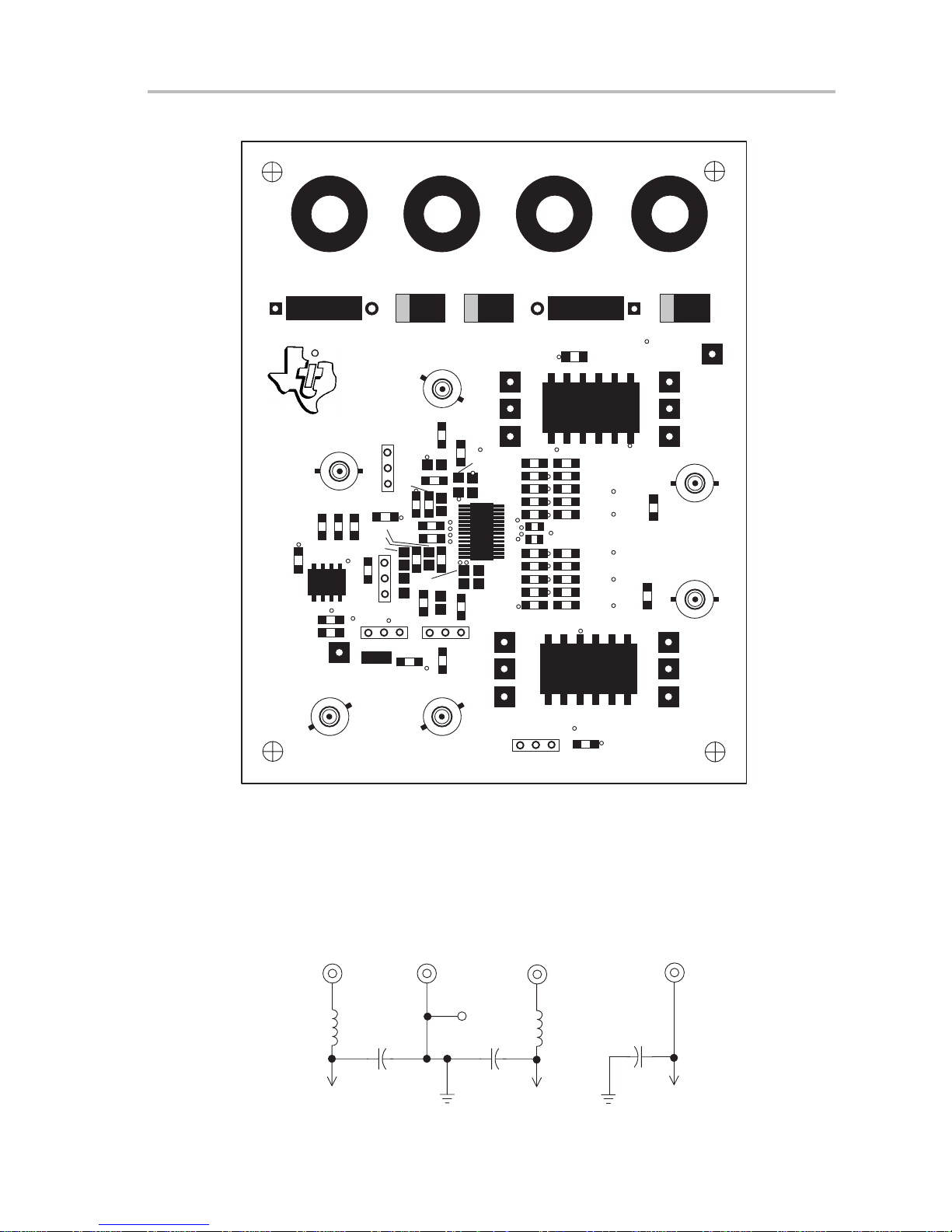
Figure 1–1.THS7002 Evaluation Module
Description
SLOP136
Rev. B
J1
+V
CC
J2
Pre-Amp A
Output
J5
1998
Input A
Texas Instruments
Input B
J6
JP1
C6
R6
1
R8
R7
R1C1 R2
C2
U2
C3
R4
U2 Out
J7
R9
C11
C10
C12
R10
C9
R3
R12
JP2
1
R13
1
R14
R16
J8
B
GND
R18
R5
C8
R11
C13
C14
JP4JP3
1
BVREF
R17
Pre-Amp B
Output
THS7002 EVM Board
J4J3
+++
CC
C17
AG2
(3)
AG1
(2)
AG0
(1)
C7
R15
VH
BS/D
R20
(6)
(5)
(4)
R23
R25
R27
U1
R29
R11
R33
R35
R37
R39
R41
1
JP5
C18
C19
R24
R26
R28
R30
R32
R34
R36
R38
R40
R42
C20
+5 V–V
S1
PGA – A
Output
R44
PGA – B
Output
R45
S2
C21L2C5C4L1
GND
AS/D
(4)
AVREF
(5)
VL
(6)
BG2
(1)
BG1
(2)
BG0
(3)
J9
J10
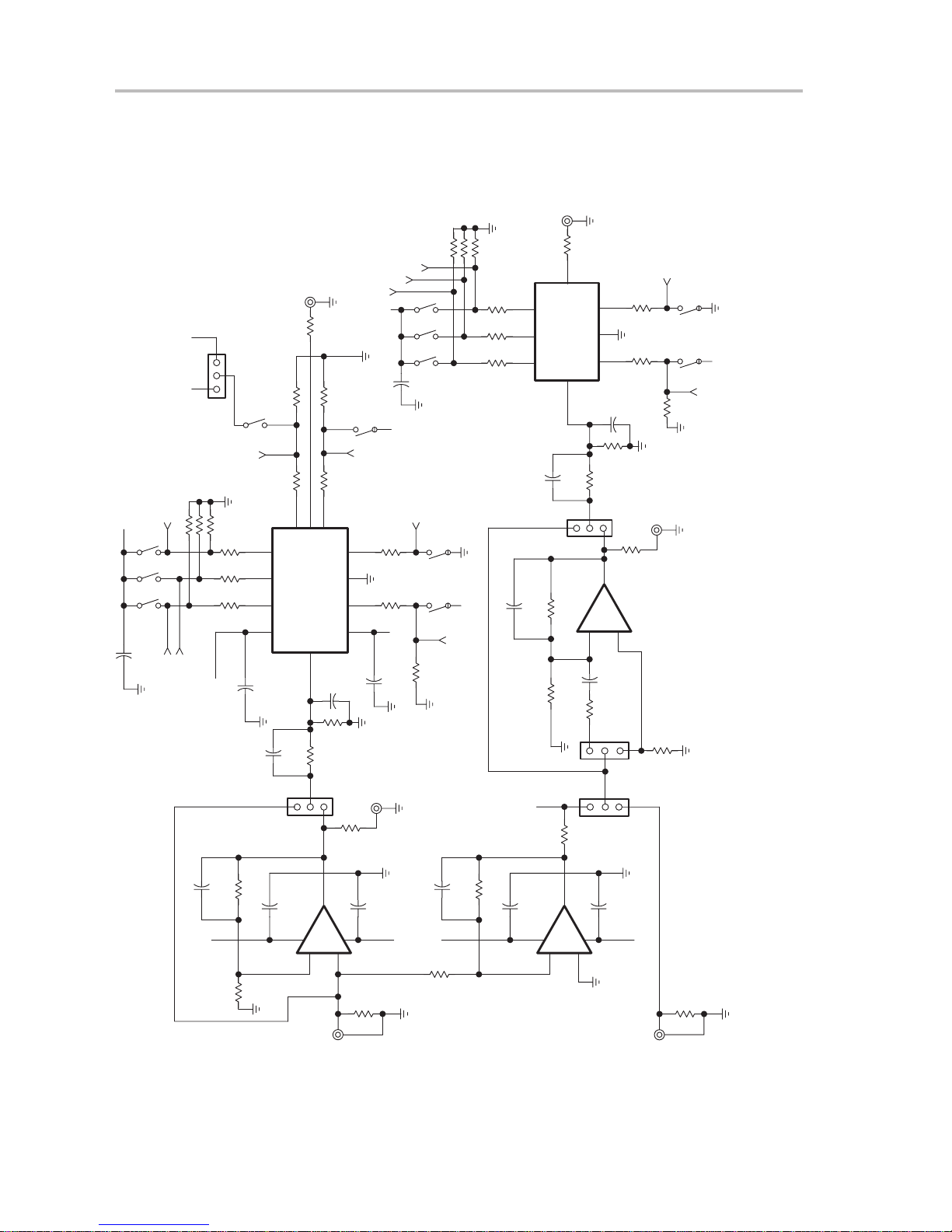
Input power is applied to the EVM through banana jacks J1, J2, J3, and J4. An
LC filter on each power bus isolates the EVM circuits from the external supply
(Figure 1–2). J4 provides a reference point for numerous circuit functions and
draws relatively little current. The schematic for the EVM amplifiers appears
in Figure 1–3.
Figure 1–2.THS7002 EVM Power Conditioning Schematic Diagram
J1
V
CC
L1
0.22 µH
15 V
C4
6.8 µF
+
J2
GND
TP1
–V
C5
6.8 µF
+
J3
CC
–15 V
L2
0.22 µH
J4
5 V
C21
6.8 µF
+
5 V
General Information
1-3
Page 10
Description
J10
PGA-B
R36, 3.3 kΩ
R38, 3.3 kΩ
R40, 3.3 kΩ
Output
5 V
C17, 0.1 µF
5 V15 V
R24, 3.3 kΩ
AG2, TP3
TP2, AG0
TP4, AG1
JP5
R26, 3.3 kΩ
R28, 3.3 kΩ
15 V
U1–D
R39, 330Ω
15
16
R37, 330Ω
17
R35, 330Ω
R11
C10, TBD
R10
TP12
U2-Out
R45
100 Ω
19
G0
G1
G2
12
R14
C14, TBD
1
499 Ω
499 Ω
R4
22 Ω
VO
VIN–
U1-C
R13
1
0 Ω
2
10
TBD
VREF
GND
SID
11
–
2
3
C9
JP3
2
13
14
18
C13
R12
9
TBD
TBD
JP4
+
TBD
3
R17
3
R15
R33
49.9 Ω
JP2
49.9 Ω
330 Ω
R34
J8
BVREF
TP14
3.3 kΩ
Pre-amp B
Output
R3
TBD
S2-E
S2-D
BS/D
5 V
TP13
Figure 1–3.THS7002 EVM Schematic Diagram
BG0, TP11
BG1, TP10
J9
PGA-A
Output
R44
R42
S2-F
R41
U1–B
26
27
28
21
C19, 0.1 µF
C6, TBD
1
100 Ω
4.7 kΩ
49.9 Ω
G2
G1
G0
R6
20
VH
VCC
0 Ω
24
3
2
VO
VIN–
JP1
R32
R31
23
VL
VREF
GND
SID
–Vcc
C7
TBD
R20
TBD
3
3
2
1
VH
TP5
R27, 330Ω
R25, 330Ω
R23, 330 Ω
BG2, TP9
5 V
C20, 0.1 µF
4.7 kΩ
S1-F
VL
TP6
49.9 Ω
R18
2
1
R29
25
22
C18, 0.1 µF
J5
Pre-amp
R5
49.9 Ω
–15 V
49.9 Ω
330 Ω
–15 V
A Out
AVREF
TP8
S2-C
S2-B
S2-A
R30
S1-E
S1-D
3.3 kΩ
AS/D
5 V
TP7
C8, TBD
15 V
R8
499 Ω
C12, 0.1 µF
R7
499 Ω
U1-A
THS7002
8
5
4
–
J6
1-4
+
6
Input A
R1
15 V
R2
1 kΩ
C3, 0.1 µF
1 kΩ
C1, TBD
C11
0.1 µF
7
–15 V
R9
49.9 Ω
U2
7
5
THS4001
–
2
C2, 0.1 µF
4
+
3
J7
–15 V
Input B
R16
49.9 Ω
General Information
Page 11

Description
The THS7002 EVM is equipped with a separate BNC input connector for each
of the two channels on the module. Each input is terminated with a 50-Ω
resistor to provide correct line impedance matching (Figure 1–3). Note that
using a source with a 50-Ω output impedance will create a voltage divider at
the EVM inputs. Thus, accurate knowledge of the source output
characteristics is required to determine proper input signal amplitudes.
The outputs of the preamplifier stages are routed through 50-Ω resistors to
provide proper cable impedance matching and termination impedance
matching. One of the drawbacks of using this type of impedance matching is
that it places an equivalent 100-Ω load on the output of the preamplifiers.
Although the preamplifier sections have a large output current capability, the
programmable gain amplifier (PGA) sections have a limited current drive
capability . It is recommended that the total impedance placed on the outputs
of the PGA section is at least 500 Ω.
The THS4001 IC and the THS7002 IC are voltage feedback amplifiers. They
follow the classic operational amplifier gain equations:
–R
Inverting Gain
+
Non-Inverting Gain+1
F
R
G
R
F
)
R
G
(1)
(2)
The gain of these amplifiers can easily be changed to support different
applications by changing the resistor ratios. Although any of the components
on the EVM board can be replaced with different values, it is imperative that
the THS7002 preamplifier gain be kept to a minimum of +2 or –1 for stability
purposes. Also, component pads have been placed in convenient locations on
the PCB (shown as components with the value X in the schematic) to allow
numerous modifications to the basic EVM configuration. However, care must
be taken because the surface-mount solder pads on the board are somewhat
fragile and will not survive a large number of soldering/desoldering operations.
For single-ended input configurations, a THS4001 is used to invert the
incoming signal to drive the second channel of the THS7002. This allows for
a single-to-differential analysis of the EVM. However, by simply moving a
jumper (JP3) and using the second input BNC connector (J7), a differential
source or independent signals can be seen on the outputs.
For independent evaluation of the preamplifiers, BNC connectors directly at
the preamplifier output pins (J5 and J8) allow the user to investigate these
amplifiers independently of the PGA sections.
General Information
1-5
Page 12

Description
The shutdown feature of the THS7002 IC is implemented on this EVM. There
is a separate shutdown pin for each half of the THS7002 IC. The shutdown
signals are low for normal THS7002 operation. When a shutdown pin is high
(5 V), the corresponding preamplifier and PGA section is turned off.
Shutdowns on the EVM are controlled by switches S1:D (A channel) and S2:D
(B channel), or by applying an external shutdown signal to test–points TP7 (A
channel) and TP13 (B channel) with the switches set to OFF . Isolation resistors
on the THS7002 IC shutdown control input pins are used to minimize surges
in the EVM environment and can be omitted in a final system design.
1-6
General Information
Page 13

Programmable Gain Amplifier Gain Control
1.3 Programmable Gain Amplifier Gain Control
Each channel of the THS7002 IC is provided with three digital control inputs
for setting the gain of the PGA stage (AG0 – AG2 and BG0 – BG2). Standard
TTL or CMOS Logic signals operate these control inputs. The gain control
inputs are not latched and respond to the control signals in real time.
Therefore, the control signals on these inputs must remain constant if the PGA
gain is to remain constant. For stand-alone evaluation of this function, onboard
DIP switches (S1:A to S1:C and S2:A to S2:C) are used to control the gain for
each PGA. Note that all DIP switch gain control elements must be set to OFF
if gain is to be set by digital control signals. For convenience, test points (TP2
– TP4 and TP9 – TP1 1) are placed on each of these lines to allow easy external
connections. There are 330-Ω isolation resistors in series with each IC gain
control input pins. These were added only for surge suppression and are not
required for actual system design. Nominal gain/attenuation is shown in
Table 1–1.
Table 1–1.THS7002 EVM PGA Nominal Gain/Attenuation
G2 G1 G0 PGA Gain (dB) PGA Gain (V/V)
0 0 0 –22 0.08
0 0 1 –16 0.16
0 1 0 –10 0.32
0 1 1 –4 0.63
1 0 0 2 1.26
1 0 1 8 2.52
1 1 0 14 5.01
1 1 1 20 10
One aspect of the THS7002 PGA signal inputs that must be considered is that
there are internal variable resistors (RF and RG) that set the gain. The
resistance of RG changes from about 270 Ω (gain = +20 dB) to about 3 kΩ
(gain = –22 dB). Therefore, any source impedance at the input to the PGA
amplifiers will cause a gain error to be seen at the output. A buffer/amplifier is
highly recommended to directly drive the input of the PGA section to help
minimize this effect.
Another consideration is that when each amplifier VREF is connected to
ground, the internal RG resistor is connected to a virtual ground. Therefore,
if a termination resistor is used on the source side, the total terminating
resistance is the parallel combination of the terminating resistance and the
internal RG resistor. This, in conjunction with the series impedance problem
mentioned previously , can potentially cause a voltage mismatch between the
output of a 50-Ω source and the expected PGA output voltage.
These points are illustrated by the following formula and in the simplified
diagram of the THS7002 PGA section shown in Figure 1–4.
R
TOTALTERMINATION
+
R
R
TERMINATION
TERMINATION
)
(R
(R
SOURCE
SOURCE
)
)
RG)
RG)
(3)
General Information
1-7
Page 14

Programmable Gain Amplifier Gain Control
Figure 1–4.Simplified PGA Section of the THS7002
No Source Impedance
V
IN
R
SOURCE
R
TERMINATION
The PGA VREF terminals are also accessible via test points TP8 and TP14.
Typically, the DIP switches are used to keep this point at ground. If a voltage
is applied to this terminal, then the output of the PGA section will amplify the
applied reference voltage by one plus the selected gain. Thus, the output gain
due only to VREF will be from +0.6 dB to +21 dB according to the following
formula:
PGA
–V
PGA
V
REF
IN
R
G
G0 G1 G
–
PGA
+
F
THS7002 IC
Positive
Clamp V
PGA
V
OUT
Negative
Clamp V
H
L
2
R
V
OUT
ǒ
Ǔ
+20
V
REF
Log
ƪ
1
)ǒPGA Gain(VńV
10
Ǔ
Ǔ
ƫ
Typically, the output of the PGA will directly drive an A/D converter. Because
of the limited linear input range and saturation characteristics of most ADCs,
the PGA outputs incorporate a voltage clamp. Because the internal clamps
use the same clamping reference voltages, the outputs of both PGAs are
clamped to the same values. These clamps are typically connected to the
power supply pins to allow a full output range. However, by setting switch S1:F
to OFF and setting switch S2:F to ON, the outputs will be clamped to either
+Vcc or +5V (depending on JP5) and ground. The outputs can be further
limited by applying an external reference voltage to test points TP5 (VH) and
TP6 (VL). The accuracy of this clamp is dependant on the amount of current
flowing through the internal clamping diodes. As is typical with all diodes, the
voltage drop across this diode increases with current. Therefore, the accuracy
of the clamp is highly dependant upon the output voltage, the clamping voltage
differences, and the output current. The 50-Ω series resistors are placed on
this EVM only for surge suppression. In a final system layout, these resistors
are not required for proper operation.
1-8
General Information
Page 15

1.4 EVM DIP Switch Functionality
S1:A
A–G0
S1:B
A–G1
S1:C
A–G2
S1:D
A–S/D
S1:E
A–VREF
S1:F
VL
S2:A
B–G2
S2:B
B–G1
S2:C
B–G0
S2:D
B–S/D
S2:E
B–VREF
S2:F
VH
The THS7002 can be fully evaluated without any external digital control
signals applied. This is accomplished through the use of two banks of DIP
switches. Each DIP switch bank incorporates six SPST switches labeled A
through F. The functionality of each switch is described in Table 1–2.
Table 1–2.EVM DIP Switch Functionality
SWITCH LABEL POSITION DESCRIPTION
0 PGA – A-Channel Gain Bit 0 (LSB): Value = 0 (Low)
1 PGA – A-Channel Gain Bit 0 (LSB): Value = 1 (High)
0 PGA – A-Channel Gain Bit 1: Value = 0 (Low)
1 PGA – A-Channel Gain Bit 1: Value = 1 (High)
0 PGA – A-Channel Gain Bit 2 (MSB): Value = 0 (Low)
1 PGA– A-Channel Gain Bit 2 (MSB): Value = 1 (High)
0 A-Channel Shutdown: Value = 0 (Low) — A Side Active
1 A-Channel Shutdown: Value = 1 (High) — A Side Shutdown
0 A-Channel VREF Floating (Connect TP8 to Ext. Ref.)
1 A-Channel VREF Connected to Ground
0 Low Side Clamp Ground (Connect TP6 to Ext Ref)
1 Low Side Clamp Connected to –Vcc
0 PGA – B-Channel Gain Bit 2 (MSB): Value = 0 (Low)
1 PGA – B-Channel Gain Bit 2 (MSB): Value = 1 (High)
0 PGA – B-Channel Gain Bit 1: Value = 0 (Low)
1 PGA – B-Channel Gain Bit 1: Value = 1 (High)
0 PGA – B-Channel Gain Bit 0 (LSB): Value = 0 (Low)
1 PGA – B-Channel Gain Bit 0 (LSB): Value = 1 (High)
0 B-Channel Shutdown: Value = 0 (Low) — B Side Active
1 B-Channel Shutdown: Value = 1 (High) — B Side Shutdown
0 B-Channel VREF Floating (Connect TP14 to Ext Ref)
1 B-Channel VREF Connected to Ground
0 High Side Clamp Ground (Connect TP5 to Ext Ref)
1 High Side Clamp Connected to JP5 (Vcc or 5 V)
EVM DIP Switch Functionality
General Information
1-9
Page 16

EVM Circuit Configuration
1.5 EVM Circuit Configuration
The THS7002 EVM design allows evaluation of each section of the THS7002
amplifier IC separately as well as a differential system. Configuration of the
EVM is accomplished through jumpers mounted on the module PCB. Each
jumper is a three-pin header that acts as an SPDT switch when a shunt is
placed across two of the three pins to select either of two signal routes (Figure
1–5).
Figure 1–5.THS7002 Evaluation Module Block Diagram
J6
J7
Input A
Input B
Preamp A
THS7002
U1:A
U2
THS4001
Inverter
JP3
2
-
Jumper JP1:
J
J
-
Jumper JP2:
PGA A
JP1
1
2
3
1
1
3
3
THS7002
2
JP2
Preamp B
VH Clamp
U1: B
U1:C
–
THS7002
+
1
3
JP5
1
2
3
JP4
2
THS7002
PGA B
5 V
15 V
U1: D
PGA A
Output
Preamp A
Output
PGA B
Output
Preamp B
Output
J9
J5
J10
J8
1–2 — Connects the input of A-channel PGA (U1: B) to the input A
BNC (J6), bypassing the THS7002 A-channel preamplifier (U1:A)
2–3 — Connects the input of A-channel PGA (U1: B) to the output of
the A-channel preamplifier (U1:A)
J
J
-
Jumper JP3:
J
J
1-10
1–2 — Connects the inverting input terminal of the B-channel
preamplifier (U1:C) to the signal from JP3 (either the THS4001
inverting amplifier (U2) output or the input B BNC (J7) signal,
depending on the setting of JP3). In order to use this functionality,
components R3, R13, and C9 must be selected and installed on the
EVM by the user
2–3 — Connects the noninverting input terminal of the B-channel
preamplifier (U1:C) to the signal from JP3
1–2 — Connects the input of the B-channel preamplifier (U1: C) or the
B-channel PGA (U1:D) to the output of the THS4001 inverting
amplifier (U2). This signal is an inverted version of the input A BNC
(J6) signal
2–3 — Connects the input of the B-channel preamplifier (U1: C) or the
B-channel PGA (U1:D) to the input B BNC (J7)
General Information
Page 17

EVM Circuit Configuration
-
Jumper JP4:
J
1–2 — Connects the input of the B-channel PGA (U1: D) to the signal
from JP3
J
2–3 — Connects the input of the B-channel PGA (U1: D) to the output
of the B-channel preamplifier (U1:C)
-
Jumper JP5:
J
1–2 — Connects the THS7002 IC positive clamp input pin (VH) to Vcc
when switch S2:F is set appropriately
J
2–3 — Connects the THS7002 IC positive clamp input pin (VH) to +5V
when switch S2:F is set appropriately
For example, to use a single-ended input and use the preamplifiers as buffers
and gain:
1) Set JP1 to 2–3
2) Set JP2 to 2–3
3) Set JP3 to 1–2
4) Set JP4 to 2–3
5) Apply the input to input A (J6)
The output of the THS7002 PGAs is a differential signal due to the inverter
(U2). For either an independent or differential signal source, JP3 should be set
to the 2–3 position.
General Information
1-1 1
Page 18

Using the THS7002 EVM
1.6 Using the THS7002 EVM
The THS7002 EVM operates from a split power supply with voltages ranging
from ±5 V to ±15 V. It also uses 5 volt logic control signals to configure the
operation of the EVM when the DIP switches are used. The use of a single
supply for this EVM is not recommended. As shipped, the preamplifiers are set
to a gain of 2 and the EVM is configured for a single-ended input that uses the
preamplifiers to directly drive the PGA stages. An oscilloscope is typically used
to view and analyze the EVM output signals.
1) Ensure that all power supplies are set to
connections to the THS7002 EVM.
2) Select the operating voltage for the EVM and connect appropriate split
power supplies to the banana jacks on the module marked
–VCC
(J3).
OFF
before making power supply
+V
CC
(J1) and
3) Connect a 5-V power supply to the banana jack marked
+5 V
4) Connect all power supply grounds to the banana jack marked
5) Connect an oscilloscope probe to the PGA–A amplifier output BNC (J9).
Connecting directly to J9 with a 50-Ω nominal impedance cable and probe
is not recommended. The output drive capability of the PGAs is very
limited. Such a connection will load the output excessively, reducing the
output voltage range of the amplifier and is not a true measurement of the
amplifier performance.
6) Set EVM jumpers as shown in Table 1–3.
Table 1–3.THS7002 EVM Jumper Settings
JP1 JP2 JP3 JP4 JP5
2–3 2–3 1–2 2–3 1–2
7) Set DIP switch 1 and 2 elements as shown in Table 1–4.
Table 1–4.THS7002 EVM DIP Switch Settings
SWITCH S1 LABEL POSITION SWITCH S2 LABEL POSITION
S1:A A–G0 0 S2:A B–G2 1
S1:B A–G1 0 S2:B B–G1 0
S1:C A–G2 1 S2:C B–G0 0
S1:D A–S/D 0 S2:D B–S/D 0
S1:E A–VREF 1 S2:E B–VREF 1
S1:F VL 1 S2:F VH 1
(J4).
GND
(J2).
8) Set the power supplies to ON.
9) Connect a signal input to the INPUT A BNC (J6).
Note that each input connector on this EVM is terminated with a 50-Ω resistor
to ground. With a 50-Ω source impedance, the voltage seen by the THS7002
amplifier IC on the EVM will be ½ the source signal voltage applied to the EVM
input connector.
10) Verify the output signal on the oscilloscope using a high-impedance probe
— a voltage gain of approximately 2.5 to 1 should be observed.
1-12
General Information
Page 19

1.7 THS7002 EVM Performance
Figure 1–6 shows the typical frequency response and Figure 1–7 shows the
typical phase response of the THS7002 EVM preamplifiers. Typical –3 dB
bandwidth with a ±15-V power supply is 100 MHz for the preamplifier in each
channel and 90 MHz with a ±5-V power supply.
Figure 1–6.THS7002 EVM Preamplifier Frequency Response
7
THS7002 EVM Performance
6
5
4
3
2
Output Amplitude – dB
1
VO = 0.4 Vp–p
RL = 150 Ω
0
100k 1M 10M 100M
VCC = ±5 V
f – Frequency – Hz
Figure 1–7.THS7002 EVM Preamplifier Phase Response
30
0
–30
VCC = ±15 V
500M
VCC = ±15 V
–60
–90
Output Phase – °
–120
–150
–180
VO = 0.4 Vp–p
RL = 150 Ω
100k
1M
f – Frequency – Hz
VCC = ±5 V
10M 100M
500M
General Information
1-13
Page 20

THS7002 EVM Performance
Figure 1–8 shows the typical frequency response and Figure 1–9 shows the
typical phase response of the THS7002 EVM PGAs. This data was collected
with the gain set to +2 dB. Typical –3 dB bandwidth is 65 MHz with a ±5-V
power supply and 70 MHz with a ±15-V power supply.
Figure 1–8.THS7002 EVM PGA Frequency Response
4
3
2
1
0
–1
Output Amplitude – dB
–2
VO = 0.4 Vp–p
RL = 500 Ω
–3
100k 1M 10M 100M
VCC = ±5 V
f – Frequency – Hz
Figure 1–9.THS7002 EVM PGA Phase Response
210
180
150
VCC = ±15 V
500M
VCC = ±15 V
1-14
120
90
Output Phase – °
60
30
VO = 0.4 Vp–p
RL = 500 Ω
0
100k
VCC = ±5 V
1M
f – Frequency – Hz
10M 100M
500M
General Information
Page 21

THS7002 EVM Performance
Figure 1–10 shows the typical frequency response and Figure 1–1 1 shows the
typical phase response of the THS7002 EVM preamplifiers + PGAs. This data
was collected with the preamplifiers directly driving the PGA inputs. The PGA
was set to a gain of +2 dB. Typical –3 dB bandwidth is 65 MHz with a ±5-V
power supply and 70 MHz with a ±15-V power supply.
Figure 1–10. THS7002 EVM Preamplifier + PGA Frequency Response
10
9
8
7
6
VCC = ±5 V
5
Output Amplitude – dB
4
VO = 0.4 Vp–p
RL = 500 Ω
3
100k 1M 10M 100M
f – Frequency – Hz
VCC = ±15 V
Figure 1–11. THS7002 EVM Preamplifier + PGA Phase Response
210
180
VCC = ±15 V
150
500M
120
90
Output Phase – °
60
VO = 0.4 Vp–p
30
RL = 500 Ω
0
100k
VCC = ±5 V
1M
f – Frequency – Hz
10M 100M
500M
General Information
1-15
Page 22

General High-Speed Amplifier Design Considerations
1.8 General High-Speed Amplifier Design Considerations
The THS7002 EVM layout has been designed and optimized for use with
high-speed signals and can be used as an example when designing THS7002
applications. Careful attention has been given to component selection,
grounding, power supply bypassing, and signal path layout. Disregard of these
basic design considerations could result in less than optimum performance of
the THS7002 dual differential line drivers and receivers IC.
Surface-mount components were selected because of the extremely low lead
inductance associated with this technology. Also, because surface-mount
components are physically small, the layout can be very compact. This helps
minimize both stray inductance and capacitance.
Tantalum power supply bypass capacitors (C4, C5, and C21) at the power
input pads help supply currents for rapid, large signal changes at the amplifier
output. The 0.1 µF power supply bypass capacitors (C2, C3, C1 1, C12, C18,
and C19) were placed as close as possible to the IC power input pins in order
to keep the PCB trace inductance to a minimum. This improves
high-frequency bypassing and reduces harmonic distortion.
A proper ground plane on both sides of the PCB should always be used with
high-speed circuit design. This provides low-inductive ground connections for
return current paths. In the area of the preamplifier input pins, however, the
ground plane was removed to minimize stray capacitance and reduce ground
plane noise coupling into these pins. This is especially important for the
inverting pin while the amplifier is operating in the noninverting mode. Because
the voltage at this pin swings directly with the noninverting input voltage, any
stray capacitance would allow currents to flow into the ground plane, causing
possible gain error and/or oscillation. Capacitance variations at the amplifier
IC input pin of less than 1 pF can significantly affect the response of the
amplifier.
In general, it is always best to keep signal lines as short and as straight as
possible. Sharp 90_ corners should generally be avoided — round corners or
a series of 45_ bends should be used, instead. Stripline techniques should
also be incorporated when signal lines are greater than 3 inches in length.
These traces should be designed with a characteristic impedance of either 50
Ω or 75 Ω, as required by the application. Such signal lines should also be
properly terminated with an appropriate resistor.
Finally , proper termination of all inputs and outputs should be incorporated into
the layout. Unterminated lines, such as coaxial cable, can appear to be a
reactive load to the amplifier IC. By terminating a transmission line with its
characteristic impedance, the amplifier’s load then appears to be purely
resistive, and reflections are absorbed at each end of the line. Another
advantage of using an output termination resistor is that capacitive loads are
isolated from the amplifier output. This isolation helps minimize the reduction
in amplifier phase-margin and improves the amplifier stability for improved
performance such as reduced peaking and settling times.
1-16
General Information
Page 23

General PowerPADt Design Considerations
1.9 General PowerPADt Design Considerations
The THS7002 IC is mounted in a special package incorporating a thermal pad
that transfers heat from the IC die directly to the PCB. The PowerP ADpackage
is constructed using a downset leadframe. The die is mounted on the
leadframe but is electrically isolated from it. The bottom surface of the
lead-frame is exposed as a metal thermal pad on the underside of the package
and makes physical contact with the PCB. Because this thermal pad is in direct
physical contact with both the die and the PCB, excellent thermal performance
can be achieved by providing a good thermal path away from the thermal pad
mounting point on the PCB.
Although there are many ways to properly heatsink this device, the following
steps illustrate the recommended approach as used on the THS7002 EVM,
which is built on a multilayer PCB with an internal ground plane.
1) Prepare the PCB with a top side etch pattern as shown in Figure 1–12.
There should be etch for the leads as well as etch for the thermal pad.
Figure 1–12. PowerPAD PCB Etch and Via Pattern
Thermal pad area (0.15 x 0.17) with 10 vias
(Via diameter = 13 mils)
2) Place 18 holes in the area of the thermal pad. These holes should be 13
mils in diameter. They are kept small so that solder wicking through the
holes is not a problem during reflow.
3) Additional vias under the package, but outside the thermal pad area, will
improve heat transfer but are not required. These holes should be 25 mils
in diameter. They may be larger because they are not in the area to be
soldered so that wicking is not a problem.
4) Connect all holes, the 18 within the thermal pad area and any others
outside the pad area, to the internal ground plane.
5) When connecting these holes to the ground plane, do not use the typical
web or spoke via connection methodology . Web connections have a high
thermal resistance connection that is useful for slowing the heat transfer
during soldering operations. This makes the soldering of vias that have
plane connections easier. However, in this application, low thermal
resistance is desired for the most efficient heat transfer. Therefore, the
holes under the THS7002 package should make their connection to the
internal ground plane with a complete connection around the entire
circumference of the plated through hole.
General Information
1-17
Page 24

General PowerPADt Design Considerations
6) The top-side solder mask should leave exposed the terminals of the
package and the thermal pad area with its holes. Any larger holes outside
the thermal pad area, but still under the package, should be covered with
solder mask.
7) Apply solder paste to the exposed thermal pad area and all of the
operational amplifier terminals.
8) With these preparatory steps in place, the THS7002 is simply placed in
position and run through the solder reflow operation as any standard
surface-mount component. This results in a part that is properly installed.
The actual thermal performance achieved with the THS7002 in its PowerP AD
package depends on the application. In the example above, if the size of the
internal ground plane is approximately 3 inches × 3 inches, then the expected
thermal coefficient, θ
power dissipation is shown in Figure 1–13 and is calculated by the following
formula:
PD+
q
JA
T
MAX–TA
ǒ
Where:
P
= Maximum power dissipation of THS7002 (watts)
D
T
= Absolute maximum junction temperature (150°C)
MAX
T
= Free-ambient air temperature (°C)
A
θ
= θ
JA
JC +
θ
CA
θJC= Thermal coefficient from die junction to case (0.72 °C/W)
θCA= Thermal coefficient from case to ambient air (°C/W)
, is about 27.8_C/W. For a given θJA, the maximum
JA
Ǔ
Figure 1–13. Maximum Power Dissipation vs. Free-Air Temperature
MAXIMUM POWER DISSIPATION
vs
FREE-AIR TEMPERATURE
9
8
7
6
5
4
3
2
Maximum Power Dissipation – W
θJA = 56.2°C/W
2 oz Trace and Copper Pad
1
without Solder
0
–40 –20 0 20 80 1006040
TA – Free-Air Temperature – °C
Tj = 150°C
PCB Size = 3” x 3”
No Air Flow
θJA = 27.9°C/W
2 oz Trace and
Copper Pad
with Solder
1-18
General Information
Page 25

General PowerPADt Design Considerations
Even though the THS7002 EVM PCB is different than the one in the example
above, the results should give an idea of how much power can be dissipated
by the PowerP AD IC package. The THS7002 EVM is a good example of proper
thermal management when using PowerPAD-mounted devices.
Correct PCB layout and manufacturing techniques are critical for achieving
adequate transfer of heat away from the PowerP AD IC package. More details
on proper board layout can be found in the
GAIN AMPLIFIER
data sheet (SLOS214). For more general information on
THS7002 PROGRAMMABLE-
the PowerPAD package and its thermal characteristics, see the Texas
Instruments Technical Brief,
PowerPAD Thermally Enhanced Package
(SLMA002).
General Information
1-19
Page 26

THS7002 EVM Specifications
1.10 THS7002 EVM Specifications
Supply voltage range, ±V
Supply current, I
Input voltage, V
CC
I
CC
Output drive, THS7002 Preamplifiers, I
Output drive, THS7002 PGA, I
O
O
±5 V to ±15 V. . . . . . . . . . . . . . . . . . . . . . . . . . . . . . . . . . . . . . . . . . . .
Continuous total power dissipation at TA = 25°C (THS7002), 4.5 W, max. . . . . . . . . . . . . . . . . . .
For complete THS7002 amplifier IC specifications and parameter measurement information, and additional application information, see the THS7002
data sheet, TI Literature Number SLOS214.
32 mA, typ. . . . . . . . . . . . . . . . . . . . . . . . . . . . . . . . . . . . . . . . . . . . . . . . . . . . . . . .
±VCC, max. . . . . . . . . . . . . . . . . . . . . . . . . . . . . . . . . . . . . . . . . . . . . . . . . . . . . . . . .
90 mA, typ. . . . . . . . . . . . . . . . . . . . . . . . . . . . . . . . . . . . .
45 mA, typ. . . . . . . . . . . . . . . . . . . . . . . . . . . . . . . . . . . . . . . . . . . .
1-20
General Information
Page 27

Chapter 2
Reference
This chapter includes a parts list and PCB layout illustrations for the THS7002
EVM.
T opic Page
2.1 THS7002 Dual Differential Line Drivers and Receivers
EVM Parts List
2.2 THS7002 EVM Board Layouts 2–3. . . . . . . . . . . . . . . . . . . . . . . . . . . . . .
2–2. . . . . . . . . . . . . . . . . . . . . . . . . . . . . . . . . . . . . . . . . . .
Reference
2-1
Page 28

THS7002 Programmable-Gain Amplifier EVM Parts List
2.1 THS7002 Programmable-Gain Amplifier EVM Parts List
Table 2–1.THS7002 EVM Parts List
Reference Description Size Qty
C4, C5, C21 CAPACITOR, 6.8 µF, CERAMIC, 20%, TANTALUM, SM 3 (SPRAGUE) 293D685X9035D2T
C2, C3,
C11, C12,
C17 – C20
L1, L2 INDUCTOR, 0.22 µH AXIAL, THRU HOLE 2 (DELEVAN) DN41221/
J5 – J10 CONNECTOR, BNC 50 OHM VERTICAL PC MOUNT,
J1 – J4 JACK, BANANA RECEPTACLE, FOR 0.025″ DIA.
JP1 – JP5 HEADER, 3 PIN, 0.1″ CTRS., 0.025″ SQ. PINS 5 (DIGI–KEY) S1021–36–5329
P1 – P5 SHORTING JUMPERS, 0.1″ CTRS, FOR 0.025″ SQ.
SW1, SW2 6PST DIP SWITCH
R6, R14 RESISTOR, 0 Ω, 1/8 W, 1% SM 1206 2
R4 RESISTOR, 22 Ω, 1/8 W, 1% SM 0805 1
R15, R18,
R31, R41
R5, R9,
R16, R17
R44, R45 RESISTOR, 100 Ω, 1/8 W, 1% SM 1206 2
R23, R25,
R27, R29,
R33, R35,
R37, R39
R7, R8,
R10, R11
R1, R2 RESISTOR, 1 KΩ, 1/8 W, 1% SM 1206 2
R24, R26,
R28, R30,
R34, R36,
R38, R40
R32, R42 RESISTOR, 4.7 K Ω, 1/10 W, 1% SM 0805 2
U1 IC, THS7002CPWP 1 (TI) THS7002CPWP
U2 IC, OP AMP, THS4001CD SOIC-8 1 (TI) THS4001CD
TP2 – TP14 TEST POINT, (RED) 13 (FARNELL) 240-345
TP1 TEST POINT, (BLACK) 1 (FARNELL) 240-333
R3, R12,
R13, R20
C1,
C6 – C10,
C13, C14
PCB1 PCB, THS7002 EVM SLOP136 1
†
The values of these components are to be determined by the user in accordance with the application requirements.
CAPACITOR, 0.1 µF, CERAMIC, 10%, SM 0805 8 (MuRata) GRM40–X7R104K25
THRU HOLE
HOLE
PINS
(CTS 219 NST Series Gold Finish)
RESISTOR, 49.9 Ω, 1/10 W, 1% SM 0805 4
RESISTOR, 49.9 Ω, 1/8 W, 1% SM 1206 4
RESISTOR, 330 Ω 1/10 W , 5% SM 0805 8
RESISTOR, 499 Ω, 1/10 W, 1% SM 0805 4
RESISTOR, 3.3 K Ω, 1/10 W, 1% SM 0805 8
RESISTOR, X OHMS, SM
CAPACITOR, X µF, 10% CERAMIC
4–40 THREAD HEX STANDOFFS 0.625” LENGTH,
0.250” OD
4–40 THREAD HEX SCREWS 4
†
†
0805 5
Manufacturer/Distributor
Part Number
(DIGI-KEY) DN41221-ND
6 (MOUSER) 523–31–5329
4 (NEWARK) 35F865
5
2 (DIGI–KEY) CT2196MST–ND
8
4 (MOUSER) 534–1804
2-2
Reference
Page 29

THS7002 EVM Board Layouts
2.2 THS7002 EVM Board Layouts
Board layout examples of the THS7002 EVM PCB are shown in the following
illustrations. They are not to scale and appear here only as a reference.
Figure 2–1.THS7002 EVM Component Placement Silkscreen and Solder Pads
SLOP136
THS7002 EVM Board
Rev. B
J1 J2 J3 J4
V
CC
GND 5 V–V
GND
CC
++
JP5
C17
C18
C19
L2
R24
R26
R28
R30
R32
R34
R36
R38
R40
R42
L1
Pre-Amp A
Output
J6
1998
J6
Input
A
C1 R1 R2
C2
C3
R4
Texas Instruments
J7
U2–Out
Input
B
JP1
C10
R10
C9
R3
U2
JP2
JP3 JP4
R16
J8
R7
R8
C12
C4
R5
C6
R6
C11
C14
R14
R13
Pre-Amp B
Output
R12
C13
C5
AG2
(3)
AG1
(2)
AG0
R18
(1)
C7C8
R20
U1
R11
R15
VH
BVREF
R17
BS/D
(6)
(5)
(4)
R23
R25
R27
R29
R35
R37
R39
R41
R31
R33
S1
PGA A
Output
R44R45
PGA B
Output
C20
S2
+
GND
C21
AS/D
(4)
AVREF
(5)
VL
(6)
BG2 (1)
BG1
(2)
BG0
(3)
J9
J10
Reference
2-3
Page 30

THS7002 EVM Board Layouts
Figure 2–2.THS7002 EVM PC Board: Top Assembly
Figure 2–3.THS7002 EVM PC Board: Top Layer
2-4
Reference
Page 31

Figure 2–4.THS7002 EVM PC Board: Bottom Layer (Top VIew)
THS7002 EVM Board Layouts
Reference
2-5
Page 32

2-6
Reference
 Loading...