

Page 1
Please be aware that an important notice concerning availability, standard warranty, and use in critical applications of Texas Instruments
www.ti.com
−
SLOS363A − AUGUST 2002 − REVISED AUGUST 2003
FEATURES
D Fully Differential Architecture
D Bandwidth: 260 MHz
D Slew Rate: 1800 V/µs
D IMD
D OIP
: −73 dBc at 30 MHz
3
: 29 dBm at 30 MHz
3
D Output Common-Mode Control
D Wide Power Supply Voltage Range: 5 V, ±5 V,
12 V, 15 V
D Input Common-Mode Range Shifted to
Include the Negative Power Supply Rail
D Power-Down Capability (THS4504)
D Evaluation Module Available
DESCRIPTION
The THS4504 and THS4505 are high-performance fully
differential amplifiers from Texas Instruments. The
THS4504, featuring power-down capability, and the
THS4505, without power-down capability, set new
performance standards for fully differential amplifiers
with unsurpassed linearity, supporting 12-bit operation
through 40 MHz. Package options include the 8-pin
SOIC and the 8-pin MSOP with PowerPAD for a
smaller footprint, enhanced ac performance, and
improved thermal dissipation capability.
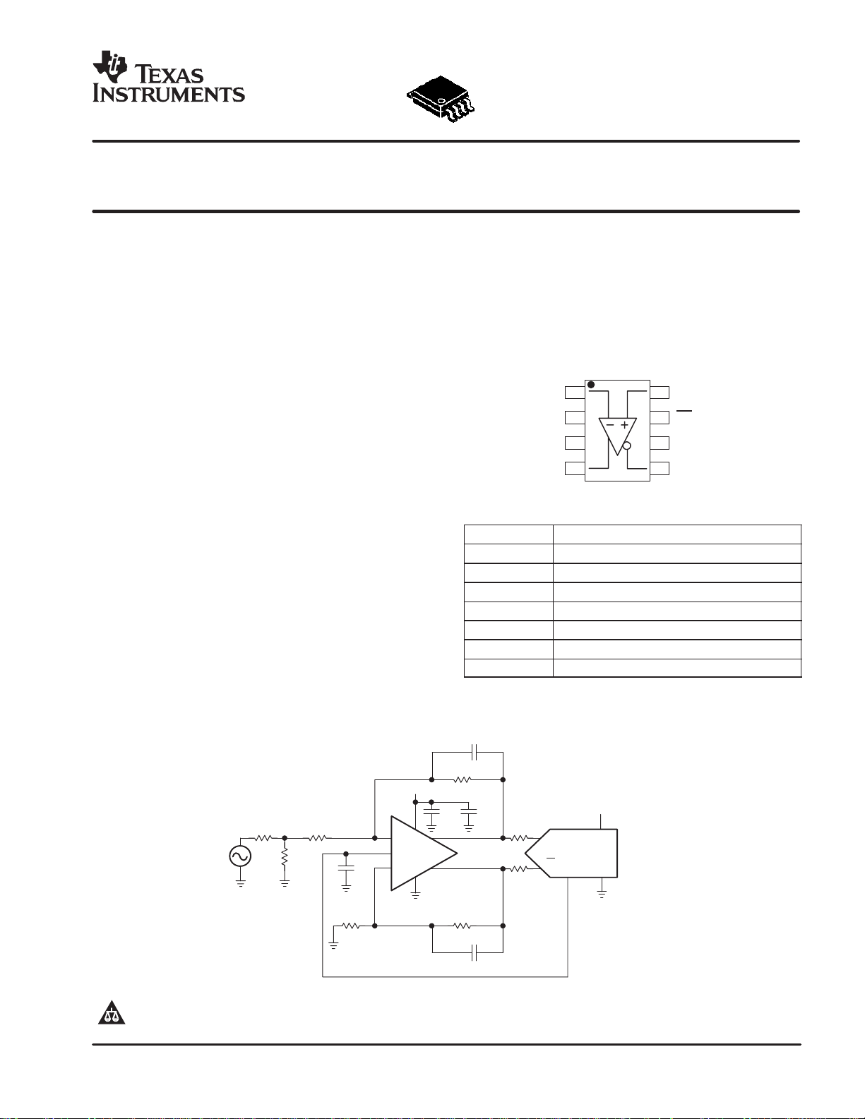
APPLICATION CIRCUIT DIAGRAM
APPLICATIONS
D High Linearity Analog-to-Digital Converter
Preamplifier
D Wireless Communication Receiver Chains
D Single-Ended to Differential Conversion
D Differential Line Driver
D Active Filtering of Differential Signals
1
V
IN−
OCM
V
S+
2
3
4
V
V
OUT+
RELATED DEVICES
DEVICE(1) DESCRIPTION
THS4504/5 260 MHz, 1800 V/µs, V
THS4500/1 370 MHz, 2800 V/µs, V
THS4502/3 370 MHz, 2800 V/µs, Centered V
THS4120/1 3.3 V , 100 MHz, 43 V/µs, 3.7 nV√Hz
THS4130/1 ±15 V, 150 MHz, 51 V/µs, 1.3 nV√Hz
THS4140/1 ±15 V, 160 MHz, 450 V/µs, 6.5 nV√Hz
THS4150/1 ±15 V, 150 MHz, 650 V/µs, 7.6 nV√Hz
(1)
Even numbered devices feature power-down capability
8.2 pF
8
7
6
5
V
IN+
PD
V
S−
V
OUT−
Includes V
ICR
Includes V
ICR
S−
S−
ICR
499 Ω
5 V
5 V
ADC
12 Bit/80 MSps
V
ref
Copyright 2002, Texas Instruments Incorporated
50 Ω
V
S
semiconductor products and disclaimers thereto appears at the end of this data sheet.
PowerPAD is a trademark of Texas Instruments.
!"# "#$" "%&$#" " '&# " &! #$" "! '$! %
!(!)'!"#* ! #$# % !$ !(! "$#! " #! '$+!,- '!%."+ #
!)!#&$) $&$#!&#*
487 Ω
53.6 Ω
1 µF
523 Ω
+
V
−
OCM
0.1 µF 10 µF
−
+
24.9 Ω
IN
IN
24.9 Ω
499 Ω
8.2 pF
Page 2
(1)
PACKAGE
θ
JC
θ
JA
(1)
Supply voltage
V
SLOS363A − AUGUST 2002 − REVISED AUGUST 2003
www.ti.com
ABSOLUTE MAXIMUM RATINGS
over operat i n g f ree-air temperature range unless otherwise noted
UNIT
Supply voltage, V
Input voltage, V
Output current, IO
S
I
(2)
Differential input voltage, V
ID
16.5 V
±V
S
150 mA
4 V
Continuous power dissipation See Dissipation Rating Table
Maximum junction temperature, T
Operating free-air temperature range, T
Storage temperature range, T
J
A
stg
Lead temperature
1,6 mm (1/16 inch) from case for 10 seconds
(1)
Stresses above these ratings may cause permanent damage.
150°C
−40°C to 85°C
−65°C to
150°C
300°C
Exposure to absolute maximum conditions for extended periods
may degrade device reliability. These are stress ratings only, and
functional operation of the device at these or any other conditions
beyond those specified is not implied.
(2)
The THS450x may incorporate a PowerPAD on the underside of
the chip. This acts as a heatsink and must be connected to a
thermally dissipative plane for proper power dissipation. Failure
to do so may result in exceeding the maximum junction
temperature which could permanently damage the device. See TI
technical brief SLMA002 for more information about utilizing the
PowerPAD thermally enhanced package.
PIN ASSIGNMENTS
THS4504
(TOP VIEW)
D AND DGN
(1)
This integrated circuit can be damaged by ESD. Texas
Instruments recommends that all integrated circuits be
handled with appropriate precautions. Failure to observe
proper handling and installation procedures can cause damage.
ESD damage can range from subtle performance degradation to
complete device failure. Precision integrated circuits may be more
susceptible t o damage because very small parametric changes could
cause the device not to meet its published specifications.
PACKAGE DISSIPATION RATINGS
θ
(°C/W)
θ
(°C/W)
D (8 pin) 38.3 167 740 mW 390 mW
DGN (8 pin) 4.7 58.4 2.14 W 1.11 W
POWER RATING
TA ≤ 25°C TA = 85°C
RECOMMENDED OPERATING CONDITIONS
MIN NOM MAX UNIT
Dual supply ±5 ±7.5
Single supply 4.5 5 15
Operating free-air temperature, TA−40 85 °C
PACKAGE/ORDERING INFORMATION
ORDERABLE PACKAGE AND NUMBER
PLASTIC
SMALL OUTLINE
(1)
(D)
THS4504D THS4504DGN BDB
THS4505D THS4505DGN BDC
(1)
This package is available taped and reeled. To order this
packaging option, add an R suffix to the part number (e.g.,
THS4504DR).
THS4505
(TOP VIEW)
PLASTIC MSOP
(DGN)
D AND DGN
PACKAGE
MARKING
V
1
IN−
V
2
OCM
V
3
S+
V
4
OUT+
V
8
IN+
7
PD
6
V
S−
V
5
OUT−
V
1
IN−
V
2
OCM
V
3
S+
V
4
OUT+
V
8
IN+
7
NC
6
V
S−
V
5
OUT−
2
Page 3
MIN/
PARAMETER
TEST CONDITIONS
MIN/
/
Small-signal bandwidth
2nd harmonic
3rd harmonic
www.ti.com
SLOS363A − AUGUST 2002 − REVISED AUGUST 2003
ELECTRICAL CHARACTERISTICS VS = ±5 V
Rf = Rg = 499 Ω, RL = 800 Ω, G = +1, Single-ended input unless otherwise noted.
THS4504 AND THS4505
TYP OVER TEMPE R ATURE
25°C 25°C
AC PERFORMANCE
G = 1, PIN= −20 dBm, Rf = 499 Ω 260 MHz Typ
G = 2, PIN= −20 dBm, Rf = 499 Ω 110 MHz Typ
G = 5, PIN= −20 dBm, Rf = 499 Ω 40 MHz Typ
G = 10, PIN = −20 dBm, Rf = 499 Ω 20 MHz Typ
Gain-bandwidth product G > +10 210 MHz Typ
Bandwidth for 0.1dB flatness PIN = −20 dBm 65 MHz Typ
Large-signal bandwidth G = 1, VP = 2 V 250 MHz Typ
Slew rate 4 VPP Step 1800 V/µs Typ
Rise time 2 VPP Step 0.8 ns Typ
Fall time 2 VPP Step 1 ns Typ
Settling time to 0.01% VO = 4 V
0.1% VO = 4 V
Harmonic distortion G = 1, VO = 2 V
Third-order intermodulation
distortion
Third-order output intercept point
Input voltage noise f > 1 MHz 8 nV/√Hz Typ
Input current noise f > 100 kHz 2 pA/√Hz Typ
Overdrive recovery time Overdrive = 5.5 V 60 ns Typ
VO = 2 VPP, fc = 30 MHz,
Rf = 499 Ω, 200 kHz tone spacing
fc = 30 MHz, Rf = 499 Ω,
Referenced to 50 Ω
PP
PP
PP
f = 8 MHz −79 dBc Typ
f = 30 MHz −66 dBc Typ
f = 8 MHz −93 dBc Typ
f = 30 MHz −65 dBc Typ
100 ns Typ
20 ns Typ
−73 dBc Typ
29 dBm Typ
0°C to
70°C
−40°C to
85°C
UNITS
TYP
MAX
Typ
DC PERFORMANCE
Open-loop voltage gain 55 52 50 50 dB Min
Input offset voltage −4 −7 / −1 −8 / 0 −9 / +1 mV Max
Average offset voltage drift ±10 ±10 µV/°C Typ
Input bias current 4 4.6 5 5.2 µA Max
Average bias current drift ±10 ±10 nA/°C Typ
Input offset current 0.5 1 2 2 µA Max
Average offset current drift ±40 ±40 nA/°C Typ
INPUT
Common-mode input range −5.7 / 2.6 −5.4 / 2.3 −5.1 / 2 −5.1 / 2 V Min
Common-mode rejection ratio 80 74 70 70 dB Min
Input impedance 107 || 1 Ω || pF Typ
OUTPUT
Differential output voltage swing RL = 1 kΩ ±8 ±7.6 ±7.4 ±7.4 V Min
Differential output current drive RL = 20 Ω 130 110 100 100 mA Min
Output balance error PIN = −20 dBm, f = 100 kHz −65 dB Typ
Closed-loop output impedance
(single-ended)
f = 1 MHz 0.1 Ω Typ
3
Page 4

MIN/
PARAMETER
TEST CONDITIONS
MIN/
/
SLOS363A − AUGUST 2002 − REVISED AUGUST 2003
ELECTRICAL CHARACTERISTICS VS = ±5 V (continued)
Rf = Rg = 499 Ω, RL = 800 Ω, G = +1, Single-ended input unless otherwise noted.
THS4504 AND THS4505
TYP OVER TEMPE R ATURE
25°C 25°C
OUTPUT COMMON-MODE VOLTAGE CONTROL
Small-signal bandwidth RL = 400 Ω 200 MHz Typ
Slew rate 2 VPP step 92 V/µs Typ
Minimum gain 1 0.98 0.98 0.98 V/V Min
Maximum gain 1 1.02 1.02 1.02 V/V Max
Common-mode offset voltage −0.4 −4.6/+3.8 −6.6/+5.8 −7.6/+6.8 mV Max
Input bias current V
Input voltage range ±4 ±3.7 ±3.4 ±3.4 V Min
Input impedance 25 || 1 kΩ || pF Typ
Maximum default voltage V
Minimum default voltage V
POWER SUPPLY
Specified operating voltage ±5 ±7.5 ±7.5 ±7.5 V Max
Maximum quiescent current 16 20 23 25 mA Max
Minimum quiescent current 16 13 11 9 mA Min
Power supply rejection (±PSRR) 80 76 73 70 dB Min
= 2.5 V 100 150 170 170 µA Max
OCM
left floating 0 0.05 0.10 0.10 V Max
OCM
left floating 0 −0.05 −0.10 −0.10 V Min
OCM
0°C to
70°C
−40°C to
85°C
www.ti.com
UNITS
TYP
MAX
POWER DOWN (THS4505 ONL Y)
Enable voltage threshold Device enabled ON above –2.9 V −2.9 V Min
Disable voltage threshold Device disabled OFF below –4.3 V −4.3 V Max
Power-down quiescent current 800 1000 1200 1200 µA Max
Input bias current 200 240 260 260 µA Max
Input impedance 50 || 1 kΩ || pF Typ
Turnon time delay 1000 ns Typ
Turnoff time delay 800 ns Typ
4
Page 5
MIN/
PARAMETER
TEST CONDITIONS
MIN/
/
Small-signal bandwidth
2nd harmonic
3rd harmonic
www.ti.com
SLOS363A − AUGUST 2002 − REVISED AUGUST 2003
ELECTRICAL CHARACTERISTICS VS = 5 V
Rf = Rg = 499 Ω, RL = 800 Ω, G = +1, Single-ended input unless otherwise noted.
THS4504 AND THS4505
TYP OVER TEMPERATURE
25°C 25°C
AC PERFORMANCE
G = 1, PIN = −20 dBm, Rf = 499 Ω 210 MHz Typ
G = 2, PIN = −20 dBm, Rf = 499 Ω 120 MHz Typ
G = 5, PIN = −20 dBm, Rf = 499 Ω 40 MHz Typ
G = 10, PIN = −20 dBm, Rf = 499 Ω 20 MHz Typ
Gain-bandwidth product G > +10 200 MHz Typ
Bandwidth for 0.1 dB flatness PIN = −20 dBm 100 MHz Typ
Large-signal bandwidth G = 1, VP = 1 V 200 MHz Typ
Slew rate 2 VPP Step 900 V/µs Typ
Rise time 2 VPP Step 1.1 ns Typ
Fall time 2 VPP Step 1 ns Typ
Settling time to 0.01% VO = 2 V Step 100 ns Typ
0.1% VO = 2 V Step 20 ns Typ
Harmonic distortion G = 1, VO = 2 V
f = 8 MHz, −77 dBc Typ
f = 30 MHz −56 dBc Typ
f = 8 MHz −74 dBc Typ
f = 30 MHz −57 dBc Typ
Third-order intermodulation
distortion
Third-order output intercept point
Input voltage noise f > 1 MHz 8 nV/√Hz Typ
Input current noise f > 100 kHz 2 pA/√Hz Typ
Overdrive recovery time Overdrive = 5.5 V 60 ns Typ
VO = 2 VPP, fc = 30 MHz,
Rf = 499 Ω, 200 kHz tone spacing
fc = 30 MHz, Rf = 499 Ω,
Referenced to 50 Ω
PP
−72 dBc Typ
28 dBm Typ
0°C to
70°C
−40°C to
85°C
UNITS
TYP
MAX
Typ
DC PERFORMANCE
Open-loop voltage gain 54 51 49 49 dB Min
Input offset voltage −4 −7 / −1 −8 / 0 −9 / +1 mV Max
Average offset voltage drift ±10 ±10 µV/°C Typ
Input bias current 4 4.6 5 5.2 µA Max
Average bias current drift ±10 ±10 nA/°C Typ
Input offset current 0.5 0.7 1.2 1.2 µA Max
Average offset current drift ±20 ±20 nA/°C Typ
INPUT
Common-mode input range −0.7/2.6 −0.4 / 2.3 −0.1 / 2 −0.1 / 2 V Min
Common-mode rejection ratio 80 74 70 70 dB Min
Input impedance 107 || 1 Ω || pF Typ
OUTPUT
Differential output voltage swing RL = 1 kΩ, Referenced to 2.5 V ±3.3 ±3 ±2.8 ±2.8 V Min
Output current drive RL = 20 Ω 110 90 80 80 mA Min
Output balance error PIN = −20 dBm, f = 100 kHz −38 dB Typ
Closed-loop output impedance
(single-ended)
f = 1 MHz 0.1 Ω Typ
5
Page 6
PARAMETER
TEST CONDITIONS
SLOS363A − AUGUST 2002 − REVISED AUGUST 2003
ELECTRICAL CHARACTERISTICS VS = 5 V (continued)
Rf = Rg = 499 Ω, RL = 800 Ω, G = +1, Single-ended input unless otherwise noted.
THS4504 AND THS4505
TYP OVER TEMPERATURE
25°C 25°C
OUTPUT COMMON-MODE VOLTAGE CONTROL
Small-signal bandwidth RL = 400 Ω 160 MHz Typ
Slew rate 2 VPP Step 80 V/µs Typ
Minimum gain 1 0.98 0.98 0.98 V/V Min
Maximum gain 1 1.02 1.02 1.02 V/V Max
Common-mode offset voltage 0.4 −2.6/3.4 −4.2/5.4 −5.6/6.4 mV Max
Input bias current V
Input voltage range 1 / 4 1.2 / 3.8 1.3 / 3.7 1.3 / 3.7 V Min
Input impedance 25 || 1 kΩ || pF Typ
Maximum default voltage V
Minimum default voltage V
POWER SUPPLY
Specified operating voltage 5 15 15 15 V Max
Maximum quiescent current 14 17 19 21 mA Max
Minimum quiescent current 14 11 10 8 mA Min
Power supply rejection (+PSRR) 75 72 69 66 dB Min
= 2.5 V 1 2 3 3 µA Max
OCM
left floating 2.5 2.55 2.6 2.6 V Max
OCM
left floating 2.5 2.45 2.4 2.4 V Min
OCM
0°C to
70°C
−40°C
to 85°C
www.ti.com
UNITS
MIN/
MAX
POWER DOWN (THS4505 ONL Y)
Enable voltage threshold Device enabled ON above 2.1 V 2.1 V Min
Disable voltage threshold Device disabled OFF below 0.7 V 0.7 V Max
Power-down quiescent current 600 800 1200 1200 µA Max
Input bias current 100 125 140 140 µA Max
Input impedance 50 || 1 kΩ || pF Typ
Turnon time delay 1000 ns Typ
Turnoff time delay 800 ns Typ
6
Page 7

www.ti.com
SLOS363A − AUGUST 2002 − REVISED AUGUST 2003
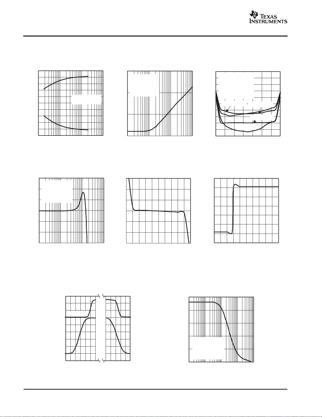
TYPICAL CHARACTERISTICS
Table of Graphs (±5 V)
Small signal unity gain frequency response 1
Small signal frequency response 2
0.1 dB gain flatness frequency response 3
Large signal frequency response 4
Harmonic distortion (single-ended input to differential output) vs Frequency 5
Harmonic distortion (single-ended input to differential output) vs Output voltage swing 6, 7
Harmonic distortion (single-ended input to differential output) vs Load resistance 8
Third order intermodulation distortion (single-ended input to differential output) vs Frequency 9
Third order output intercept point vs Frequency 10
Slew rate vs Differential output voltage step 11
Settling time 12, 13
Large signal transient response 14
Small signal transient response 15
Overdrive recovery 16, 17
Voltage and current noise vs Frequency 18
Rejection ratios vs Frequency 19
Rejection ratios vs Case temperature 20
Output balance error vs Frequency 21
Open-loop gain and phase vs Frequency 22
Open-loop gain vs Case temperature 23
Input bias offset current vs Case temperature 24
Quiescent current vs Supply voltage 25
Input offset voltage vs Case temperature 26
Common-mode rejection ratio vs Input common-mode range 27
Output voltage vs Load resistance 28
Closed-loop output impedance vs Frequency 29
Harmonic distortion (single-ended and differential input to differential output) vs Output common-mode voltage 30
Small signal frequency response at V
Output offset voltage at V
Quiescent current vs Power-down voltage 33
Turnon and turnoff delay times 34
Single-ended output impedance in power down vs Frequency 35
Power-down quiescent current vs Case temperature 36
Power-down quiescent current vs Supply voltage 37
OCM
OCM
vs Output common-mode voltage 32
FIGURE
31
7
Page 8

SLOS363A − AUGUST 2002 − REVISED AUGUST 2003
TYPICAL CHARACTERISTICS
Table of Graphs (5 V)
Small signal unity gain frequency response 38
Small signal frequency response 39
0.1 dB gain flatness frequency response 40
Large signal frequency response 41
Harmonic distortion (single-ended input to differential output) vs Frequency 42
Harmonic distortion (single-ended input to differential output) vs Output voltage swing 43, 44
Harmonic distortion (single-ended input to differential output) vs Load resistance 45
Third-order intermodulation distortion vs Frequency 46
Third-order intercept point vs Frequency 47
Slew rate vs Differential output voltage step 48
Settling time 49, 50
Overdrive recovery 51, 52
Large-signal transient response 53
Small-signal transient response 54
Voltage and current noise vs Frequency 55
Rejection ratios vs Frequency 56
Rejection ratios vs Case temperature 57
Output balance error vs Frequency 58
Open-loop gain and phase vs Frequency 59
Open-loop gain vs Case temperature 60
Input bias offset current vs Case temperature 61
Quiescent current vs Supply voltage 62
Input offset voltage vs Case temperature 63
Common-mode rejection ratio vs Input common-mode range 64
Output voltage vs Load resistance 65
Closed-loop output impedance vs Frequency 66
Harmonic distortion (single-ended and differential input) vs Output common-mode voltage 67
Small signal frequency response at V
Output offset voltage vs Output common-mode voltage 69
Quiescent current vs Power-down voltage 70
Turnon and turnoff delay times 71
Single-ended output impedance in power down vs Frequency 72
Power-down quiescent current vs Case temperature 73
Power-down quiescent current vs Supply voltage 74
OCM
www.ti.com
FIGURE
68
8
Page 9
www.ti.com
SLOS363A − AUGUST 2002 − REVISED AUGUST 2003
TYPICAL CHARACTERISTICS (±5 V Graphs)
SMALL SIGNAL UNITY GAIN FREQUENCY
RESPONSE
1
0.5
0
−0.5
−1
−1.5
−2
Gain = 1
−2.5
RL = 800 Ω
Rf = 499 Ω
−3
Small Signal Unity Gain − dB
PIN = −20 dBm
−3.5
VS = ±5 V
−4
0.1 1 10 100 1000
f − Frequency − MHz
Figure 1
LARGE SIGNAL FREQUENCY RESPONSE
25
Gain = 10, Rf = 1.8 kΩ
20
Gain = 5, Rf = 1.8 kΩ
15
10
Gain = 2, Rf = 1.8 kΩ
5
Large Signal Gain − dB
Gain = 1, Rf = 499 Ω
0
−5
0.1 1 10 100 1000
f − Frequency − MHz
RL = 800 Ω
VO = 2 V
VS = ±5 V
PP
Figure 4
SMALL SIGNAL FREQUENCY RESPONSE
22
Gain = 10
20
18
16
Gain = 5
14
12
10
8
Gain = 2
6
RL = 800 Ω
4
Small Signal Gain − dB
Rf =499 Ω
2
PIN = −20 dBm
0
VS = ±5 V
−2
0.1 1 10 100 1000
f − Frequency − MHz
Figure 2
HARMONIC DISTORTION
vs
FREQUENCY
0
Single-Ended Input to
−10
Differential Output
Gain = 1
−20
RL = 800 Ω
−30
Rf = 499 Ω
VO = 2 V
−40
−50
−60
−70
−80
Harmonic Distortion − dBc
−90
−100
0.1 1 10 100
VS = ±5 V
PP
HD2
HD3
f − Frequency − MHz
Figure 5
0.1 dB GAIN FLATNESS
FREQUENCY RESPONSE
0.05
Rf = 499 Ω
0
−0.05
−0.1
−0.15
Gain = 1
−0.2
−0.25
−0.3
RL = 800 Ω
PIN = −20 dBm
VS = ±5 V
1
10 100 1000
f − Frequency − MHz
0.1 dB Gain Flatness − dB
Figure 3
HARMONIC DISTORTION
vs
OUTPUT VOLTAGE SWING
0
Single-Ended Input to
−10
Differential Output
Gain = 1
−20
RL = 800 Ω
−30
Rf = 499 Ω
f= 8 MHz
−40
VS = ±5 V
−50
−60
−70
−80
Harmonic Distortion − dBc
−90
−100
0 0.5 1 1.5 2 2.5 3 3.5 4 4.5 5
VO − Output Voltage Swing − V
HD2
Figure 6
HD3
HARMONIC DISTORTION
vs
OUTPUT VOLTAGE SWING
0
Single Input to
−10
Differential Output
Gain = 1
−20
RL = 800 Ω
−30
Rf = 499 Ω
f= 30 MHz
−40
VS = ±5 V
−50
−60
−70
−80
Harmonic Distortion − dBc
−90
−100
HD3
0 0.5 1 1.5 2 2.5 3 3.5 4 4.5 5
VO − Output Voltage Swing − V
Figure 7
HD2
HARMONIC DISTORTION
vs
LOAD RESISTANCE
0
−10
−20
−30
−40
−50
−60
−70
Harmonic Distortion − dBc
−80
−90
HD3, 8 MHz
−100
0 400 800 1200 1600
RL − Load Resistance − Ω
HD3, 30 MHz
Single-Ended Input to
Differential Output
Gain = 1
VO = 2 V
PP
Rf = 499 Ω
VS = ±5 V
HD2, 30 MHz
HD2, 8 MHz
Figure 8
THIRD-ORDER INTERMODULATION
DISTORTION
vs
FREQUENCY
−30
Single-Ended Input to
Differential Output
−40
Gain = 1
RL = 800 Ω
−50
Rf = 499 Ω
VS = ±5 V
−60
−70
−80
−90
−100
Third-Order Intermodulation Distortion − dBc
10 100
f − Frequency − MHz
VO = 2 V
PP
VO = 1 V
200 kHz Tone Spacing
Figure 9
PP
9
Page 10
E
SLOS363A − AUGUST 2002 − REVISED AUGUST 2003
TYPICAL CHARACTERISTICS (±5 V Graphs)
www.ti.com
THIRD-ORDER OUTPUT INTERCEPT
POINT
vs
60
50
40
30
20
10
3
0
OIP − Third-Order Output Intersept Point − dBm
0 20 40 60 80 100
FREQUENCY
Gain = 1
Rf = 499 Ω
VO = 2 V
VS = ± 5 V
200 kHz Tone Spacing
Normalized to 200 Ω
200 kHz Tone Spacing
f − Frequency − MHz
PP
Normalized to 50 Ω
RL = 800 Ω
Figure 10
SETTLING TIME
3
2
1
0
−1
− Output Voltage − V
O
V
−2
−3
0 5 10 15 20 25 30 35 40
Rising Edge
Gain = 1
RL = 800 Ω
Rf = 499 Ω
f= 1 MHz
VS = ±5 V
t − Time − ns
Falling Edge
SLEW RATE
vs
DIFFERENTIAL OUTPUT VOLTAGE STEP
2000
Gain = 1
1800
RL = 800 Ω
Rf = 499 Ω
1600
sµ
VS = ±5 V
1400
V/
1200
1000
800
600
SR − Slew Rate −
400
200
0
0.5 1 1.5 2 2.5 3 3.5 4 4.5 50
VO − Differential Output Voltage Step − V
Fall
Rise
Figure 11
LARGE-SIGNAL TRANSIENT RESPONSE
2
1.5
1
0.5
0
−0.5
− Output Voltage − V
O
−1
V
−1.5
−2
−100 0 100 200 300 400 500
Gain = 1
RL = 800 Ω
Rf = 499 Ω
tr/tf = 300 ps
VS = ±5 V
t − Time − ns
1.5
1
0.5
0
−0.5
− Output Voltage − V
O
V
−1
−1.5
0 50 100 150 200 250 300
SETTLING TIME
Rising Edge
Gain = 1
RL = 800 Ω
Rf = 499 Ω
f= 1 MHz
VS = ±5 V
Falling Edge
t − Time − ns
Figure 12
SMALL-SIGNAL TRANSIENT RESPONS
0.4
0.3
0.2
0.1
0
−0.1
− Output Voltage − V
O
−0.2
V
−0.3
−0.4
−100 0 100 200 300 400 500
Gain = 1
RL = 800 Ω
Rf = 499 Ω
tr/tf = 300 ps
VS = ±5 V
t − Time − ns
OVERDRIVE RECOVERY
5
Gain = 4
4
RL = 800 Ω
Rf = 499 Ω
3
Overdrive = 4.5 V
2
VS = ±5 V
1
0
−1
−2
−3
Single-Ended Output Voltage − V
−4
−5
0 0.1 0.2 0.3 0.4 0.5 0.6
10
Figure 13
t − Time − µs
Figure 16
0.7 0.8 0.9 1
2.5
2
1.5
1
0.5
0
−0.5
−1
−1.5
−2
−2.5
Figure 14
OVERDRIVE RECOVERY
6
Gain = 4
5
RL = 800 Ω
4
Rf = 499 Ω
Overdrive = 5.5 V
3
VS = ±5 V
2
1
0
−1
−2
− Input Voltage − VV
I
−3
−4
Single-Ended Output Voltage − V
−5
−6
0 0.1 0.2 0.3 0.4 0.5 0.6 0.7 0.8 0.9 1
t − Time − µs
Figure 17
3
2
1
0
−1
−2
−3
Figure 15
VOLTAGE AND CURRENT NOISE
vs
FREQUENCY
100
nV/ Hz
10
− Input Voltage − VV
I
− Voltage Noise −
n
V
1
0.01 0.1 1 10 100
f − Frequency − kHz
Figure 18
V
n
I
n
1000 10 k
pA/ Hz
− Current Noise −
n
I
Page 11
www.ti.com
0
INPUT OFFSET VOLTAGE
COMMON-MODE REJECTION RATIO
SLOS363A − AUGUST 2002 − REVISED AUGUST 2003
TYPICAL CHARACTERISTICS (±5 V Graphs)
REJECTION RATIOS
vs
90
80
70
60
50
40
30
20
Rejection Ratios − dB
10
0
−10
0.1 1 10 100
FREQUENCY
PSRR−
RL = 800 Ω
VS = ±5 V
f − Frequency − MHz
PSRR+
CMMR
Figure 19
OPEN-LOOP GAIN AND PHASE
vs
60
50
40
30
20
Open-Loop Gain − dB
10
0
0.01 0.1 1 10 100 1000
FREQUENCY
Gain
Phase
f − Frequency − MHz
PIN = −30 dBm
RL = 800 Ω
VS = ±5 V
Figure 22
Rejection Ratios − dB
30
0
−30
°
−60
Phase −
−90
Open-Loop Gain − dB
−120
−150
REJECTION RATIOS
vs
120
100
CASE TEMPERATURE
CMMR
80
60
40
20
0
−40−30−20−10 0 10 20 30 40 50 60 70 80 90
PSRR+
RL = 800 Ω
VS = ±5 V
Case Temperature − °C
Figure 20
OPEN-LOOP GAIN
vs
CASE TEMPERATURE
58
57
56
55
54
53
52
51
50
49
−40−30−20−10 0 10 20 30 40 50 60 70 80 9
Case Temperature − °C
RL = 800 Ω
VS = ±5 V
Figure 23
OUTPUT BALANCE ERROR
vs
10
0
−10
−20
−30
−40
−50
−60
Output Balance Error − dB
−70
−80
0.1 1 10 100
FREQUENCY
PIN = 16 dBm
RL = 800 Ω
Rf = 499 Ω
VS = ±5 V
f − Frequency − MHz
Figure 21
INPUT BIAS AND OFFSET CURRENT
vs
CASE TEMPERATURE
3.4
VS = ±5 V
3.3
Aµ
3.2
3.1
3
2.9
2.8
− Input Bias Current −
2.7
IB
I
2.6
2.5
−40−30−20−100 10 20 30 40 50 60 70 80 90
I
Case Temperature − °C
IB+
I
IB−
I
OS
Figure 24
0
−0.01
Aµ
−0.02
−0.03
−0.04
−0.05
−0.06
− Input Offset Current −
−0.07
OS
I
−0.08
−0.09
QUIESCENT CURRENT
25
20
15
10
Quiescent Current − mA
5
0
SUPPLY VOLTAGE
0 0.5 1 1.5 2 2.5 3 3.5 4 4.5 5
VS − Supply Voltage − ±V
Figure 25
vs
TA = 85°C
TA = 25°C
TA = −40°C
CASE TEMPERATURE
5
VS = ±5 V
4
3
2
− Input Offset Voltage − mV
1
OS
V
0
−40−30−20−10 0 10 20 30 40 50 60 70 80 90
Case Temperature − °C
Figure 26
vs
INPUT COMMON-MODE RANGE
110
100
90
80
70
60
50
40
30
20
10
0
−10
CMRR − Common-Mode Rejection Ratio − dB
−6 −5 −4 −3 −2 −1 0 1 2 3 4 5 6
Input Common-Mode Voltage Range − V
VS = ±5 V
Figure 27
vs
11
Page 12
E
SLOS363A − AUGUST 2002 − REVISED AUGUST 2003
TYPICAL CHARACTERISTICS (±5 V Graphs)
www.ti.com
OUTPUT VOLTAGE
vs
LOAD RESISTANCE
5
4
3
2
1
0
−1
− Output Voltage − VV
−2
O
−3
−4
−5
10 100 1000
RL − Load Resistance − Ω
VS = ±5 V
TA = −40 to 85°C
10000
Figure 28
SMALL SIGNAL FREQUENCY RESPONS
at V
3
− dB
Gain = 1
RL = 400 Ω
OCM
2
Rf = 499 Ω
PIN= −20 dBm
VS = ±5 V
1
0
−1
−2
−3
1 10 100 1000
Small Signal Frequency Response at V
OCM
f − Frequency − MHz
CLOSED-LOOP OUTPUT IMPEDANCE
vs
100
Ω
10
1
− Closed Loop Output Impedance −
O
0.1
Z
FREQUENCY
Gain = 1
RL = 400 Ω
Rf = 499 Ω
VI = −4 dBm
VS = ±5 V
0.1 1 10 100
f − Frequency − MHz
Figure 29
OUTPUT OFFSET VOLTAGE at V
OCM
vs
OUTPUT COMMON-MODE VOLTAGE
600
400
200
0
−200
− Output Offset Voltage − mV
−400
OS
V
−600
−5 −4 −3 −2 −1 0 1 2 3 4 5
VOC − Output Common-Mode Voltage − V
HARMONIC DISTORTION
vs
OUTPUT COMMON-MODE VOLTAGE
0
Single-Ended to
−10
Differential Output
Gain = 1
−20
VO = 2 V
−30
−40
−50
−60
−70
−80
Harmonic Distortion − dBc
−90
−100
−3.5 −2.5 −1.5 −0.5 0.5 1.5 2.5 3.5
V
OCM
PP
Rf = 499 Ω
VS = ±5 V
HD3, 30 MHz
− Output Common-Mode Voltage − V
HD2, 30 MHz
HD2, 8 MHz
HD2, 3 MHz
Figure 30
QUIESCENT CURRENT
vs
POWER-DOWN VOLTAGE
30
25
20
15
10
5
Quiescent Current − mA
0
−5
−5 −4.5 −4 −3.5 −3 −2.5 −2 −1.5 −1 −0.5 0
Power-Down Voltage − V
12
Figure 31
TURNON AND TURNOFF DELAY TIME
Current
0
−1
−2
−3
−4
Powerdown Voltage Signal − V
−5
−6
0 0.5 1 2
1.5 2.5 3
t − Time − ms
100.5101 102 103
Figure 34
Figure 32
0.03
0.02
0.01
0
Quiescent Current − mA
Figure 33
SINGLE-ENDED OUTPUT IMPEDANCE
IN POWER DOWN
vs
FREQUENCY
1500
1200
Ω
900
600
Gain = 1
in Powerdown −
RL = 800 Ω
Rf = 499 Ω
300
− Single-Ended Output Impedance
O
Z
VI = −1 dBm
VS = ±5 V
0
0.1 1 10 100 1000
f − Frequency − MHz
Figure 35
Page 13

www.ti.com
SLOS363A − AUGUST 2002 − REVISED AUGUST 2003
TYPICAL CHARACTERISTICS (±5 V Graphs)
POWER-DOWN QUIESCENT CURRENT
vs
1000
Aµ
Power-Down Quiescent Current −
CASE TEMPERATURE
RL = 800 Ω
900
VS = ±5 V
800
700
600
500
400
300
200
100
0
−40−30−20−10 0 10 20 30 40 50 60 70 80 90
Case Temperature − °C
Figure 36
POWER-DOWN QUIESCENT CURRENT
vs
1000
900
800
700
600
500
400
300
200
100
Power-Down Quiescent Current − Aµ
SUPPLY VOLTAGE
RL = 800 Ω
0
0 0.5 1 1.5 2 2.5 3 3.5 4 4.5 5
VS − Supply Voltage − ±V
Figure 37
13
Page 14

E
SLOS363A − AUGUST 2002 − REVISED AUGUST 2003
TYPICAL CHARACTERISTICS (5 V Graphs)
www.ti.com
SMALL SIGNAL UNITY GAIN FREQUENCY
RESPONSE
1
0
−1
−2
Gain = 1
RL = 800 Ω
Rf = 499 Ω
−3
Small Signal Unity Gain − dB
PIN = −20 dBm
VS = 5 V
−4
0.1 1 10 100 1000
f − Frequency − MHz
Figure 38
LARGE SIGNAL FREQUENCY RESPONSE
25
Gain = 10, Rf = 1.8 kΩ
20
Gain = 5, Rf = 1.8 kΩ
15
10
Gain = 2, Rf = 1.8 kΩ
5
Large Signal Gain − dB
Gain = 1, Rf = 1.8 kΩ
0
−5
0.1 1 10 100 1000
f − Frequency − MHz
RL = 800 Ω
VO = 2 V
VS = 5 V
PP
Figure 41
SMALL SIGNAL FREQUENCY RESPONS
22
Gain = 10
20
18
16
Gain = 5
14
12
10
8
Gain = 2
6
RL = 800 Ω
4
Small Signal Gain − dB
Rf = 499 Ω
2
PIN = −20 dBm
0
VS = 5 V
−2
0.1 1 10 100 1000
f − Frequency − MHz
Figure 39
HARMONIC DISTORTION
vs
FREQUENCY
0
Single-Ended Input to
−10
Differential Output
Gain = 1
−20
RL = 800 Ω
−30
Rf = 499 Ω
VO = 2 V
−40
−50
−60
−70
−80
Harmonic Distortion − dBc
−90
−100
0.1 1 10 100
VS = 5 V
PP
HD3
HD2
f − Frequency − MHz
Figure 42
0.1 dB GAIN FLATNESS
FREQUENCY RESPONSE
0.05
0
Gain = 1
RL = 800 Ω
PIN = −20 dBm
VS = 5 V
1
Rf = 499 Ω
10 100 1000
f − Frequency − MHz
−0.05
−0.1
−0.15
−0.2
0.1 dB Gain Flatness − dB
−0.25
−0.3
Figure 40
HARMONIC DISTORTION
vs
OUTPUT VOLTAGE SWING
0
Single-Ended Input to
−10
Differential Output
Gain = 1
−20
RL = 800 Ω
−30
Rf = 499 Ω
f= 8 MHz
−40
VS = 5 V
−50
−60
−70
−80
Harmonic Distortion − dBc
−90
−100
00 0.5 1 1.5 2 2.5 3 3.5 4
VO − Output Voltage Swing − V
HD3
HD2
Figure 43
HARMONIC DISTORTION
vs
OUTPUT VOLTAGE SWING
0
Single-Ended Input to
−10
Differential Output
Gain = 1
−20
RL = 800 Ω
−30
Rf = 499 Ω
f= 30 MHz
−40
VS = 5 V
−50
−60
−70
−80
Harmonic Distortion − dBc
−90
−100
HD3
0 0.5 1 1.5 2 2.5 3 3.5 4
VO − Output Voltage Swing − V
Figure 44
14
HARMONIC DISTORTION
vs
LOAD RESISTANCE
0
−10
−20
−30
HD2
−40
−50
−60
−70
Harmonic Distortion − dBc
−80
−90
−100
HD3, 30 MHz
HD3, 8 MHz
0 400 800 1200 1600
RL − Load Resistance − Ω
Single-Ended Input to
Differential Output
Gain = 1
VO = 2 V
PP
Rf = 499 Ω
VS = ±5 V
HD2, 30 MHz
HD2, 8 MHz
−30
−40
−50
−60
−70
−80
−90
−100
Third-Order Intermodulation Distortion − dBc
10 100
Figure 45
DISTORTION
vs
FREQUENCY
Single-Ended Input to
Differential Output
Gain = 1
RL = 800 Ω
Rf = 499 Ω
VS = 5 V
200 kHz Tone Spacing
f − Frequency − MHz
Figure 46
VO = 2 V
VO = 1 V
PP
PP
THIRD-ORDER INTERMODULATION
Page 15

www.ti.com
E
E
SLOS363A − AUGUST 2002 − REVISED AUGUST 2003
TYPICAL CHARACTERISTICS (5 V Graphs)
THIRD-ORDER OUTPUT INTERCEPT
POINT
vs
60
50
40
30
20
10
3
0
OIP − Third-Order Output Intersept Point − dBm
FREQUENCY
Gain = 1
Rf = 499 Ω
VO = 2 V
PP
VS = 5 V
200 kHz Tone Spacing
Normalized to 50 Ω
Normalized to 200 Ω
RL = 800 Ω
0 20 40 60 80 100
f − Frequency − MHz
Figure 47
SETTLING TIME
3
Rising Edge
2
t − Time − ns
Gain = 1
RL = 800 Ω
Rf = 499 Ω
f= 1 MHz
VS = 5 V
Falling Edge
1
0
−1
− Output Voltage − V
O
V
−2
−3
0 5 10 15 20 25 30 35 40
SLEW RATE
vs
DIFFERENTIAL OUTPUT VOLTAGE STEP
1200
Gain = 1
RL = 800 Ω
1000
Rf = 499 Ω
sµ
VS = 5 V
V/
800
600
400
SR − Slew Rate −
200
0
0.5 1 1.5 2 2.5 3 3.5 40
VO − Differential Output Voltage Step − V
Fall
Rise
Figure 48
OVERDRIVE RECOVERY
5
Gain = 4
4
RL = 800 Ω
Rf = 499 Ω
3
Overdrive = 4.5 V
2
VS = ±5 V
1
0
−1
−2
−3
Single-Ended Output Voltage − V
−4
−5
0 0.1 0.2 0.3 0.4 0.5 0.6
t − Time − µs
0.7 0.8 0.9 1
2.5
2
1.5
1
0.5
0
−0.5
−1
−1.5
−2
−2.5
1.5
1
0.5
0
−0.5
− Output Voltage − V
O
V
−1
−1.5
50 100 150 200 250 300
0
t − Time − ns
Figure 49
OVERDRIVE RECOVERY
6
Gain = 4
5
RL = 800 Ω
4
Rf = 499 Ω
Overdrive = 5.5 V
3
VS = ±5 V
2
1
0
−1
−2
− Input Voltage − VV
I
−3
−4
Single-Ended Output Voltage − V
−5
−6
SETTLING TIME
0 0.1 0.2 0.3 0.4 0.5 0.6 0.7 0.8 0.9 1
t − Time − µs
Rising Edge
Gain = 1
RL = 800 Ω
Rf = 499 Ω
f= 1 MHz
VS = 5 V
Falling Edge
3
2
1
0
−1
− Input Voltage − VV
I
−2
−3
Figure 50
LARGE-SIGNAL TRANSIENT RESPONS
2
1.5
1
0.5
0
−0.5
− Output Voltage − V
O
−1
V
−1.5
−2
−100 0 100 200 300 400 500
Gain = 1
RL = 800 Ω
Rf = 499 Ω
tr/tf = 300 ps
VS = ±5 V
t − Time − ns
Figure 53
Figure 51
SMALL-SIGNAL TRANSIENT RESPONS
0.4
0.3
0.2
0.1
0
−0.1
− Output Voltage − V
O
−0.2
V
−0.3
−0.4
−100 0 100 200 300 400 500
Gain = 1
RL = 800 Ω
Rf = 499 Ω
tr/tf = 300 ps
VS = ±5 V
t − Time − ns
Figure 54
Figure 52
VOLTAGE AND CURRENT NOISE
vs
FREQUENCY
100
nV/ Hz
10
− Voltage Noise −
n
V
1
0.01 0.1 1 10 100
f − Frequency − kHz
I
n
Figure 55
V
n
1000 10 k
− Current Noise − pA/ Hz
I
15
n
Page 16

0
0
0
Open-Loop Gain − dB
Phase −
SLOS363A − AUGUST 2002 − REVISED AUGUST 2003
TYPICAL CHARACTERISTICS (5 V Graphs)
www.ti.com
REJECTION RATIOS
vs
90
80
70
60
50
40
30
20
Rejection Ratios − dB
10
0
−10
0.1 1 10 100
FREQUENCY
PSRR−
RL = 800 Ω
VS = 5 V
f − Frequency − MHz
PSRR+
CMMR
Figure 56
OPEN-LOOP GAIN AND PHASE
vs
60
50
40
30
20
10
0
0.01 0.1 1 10 100 1000
FREQUENCY
Gain
Phase
f − Frequency − MHz
PIN = −30 dBm
RL = 800 Ω
VS = 5 V
Figure 59
30
0
−30
−60
−90
−12
−15
REJECTION RATIOS
CASE TEMPERATURE
120
100
PSRR−
80
60
40
Rejection Ratios − dB
20
0
−40−30−20−10 0 10 20 30 40 50 60 70 80 90
PSRR+
Case Temperature − °C
Figure 57
OPEN-LOOP GAIN
vs
CASE TEMPERATURE
57
56
55
54
°
53
52
51
50
49
Open-Loop Gain − dB
48
47
46
−40−30−20−100 10 20 30 40 50 60 70 80 90
Case Temperature − °C
Figure 60
vs
CMMR
RL = 800 Ω
VS = 5 V
RL = 800 Ω
VS = 5 V
OUTPUT BALANCE ERROR
vs
FREQUENCY
0
PIN = 16 dBm
−10
RL = 800 Ω
Rf = 499 Ω
−20
VS = 5 V
−30
−40
−50
−60
Output Balance Error − dB
−70
−80
0.1 1 10 10
f − Frequency − MHz
Figure 58
INPUT BIAS AND OFFSET CURRENT
vs
CASE TEMPERATURE
3.75
VS = 5 V
Aµ
3.5
3.25
3
2.75
2.5
2.25
− Input Bias Current −
2
IB
I
1.75
1.5
1.25
−40−30−20−10 0 10 20 30 40 50 60 70 80 90
Case Temperature − °C
I
IB+
I
IB−
I
OS
Figure 61
0
−0.01
Aµ
−0.02
−0.03
−0.04
−0.05
−0.06
−0.07
− Input Offset Current −
−0.08
OS
I
−0.09
−0.1
Quiescent Current − mA
16
QUIESCENT CURRENT
vs
25
20
15
10
5
0
SUPPLY VOLTAGE
TA = 85°C
TA = 25°C
TA = −40°C
0 0.5 1 1.5 2 2.5 3 3.5 4 4.5 5
VS − Supply Voltage − ±V
Figure 62
INPUT OFFSET VOLTAGE
vs
CASE TEMPERATURE
5
VS = 5 V
4
3
2
− Input Offset Voltage − mV
1
OS
V
0
−40−30−20−10 0 10 20 30 40 50 60 70 80 90
Case Temperature − °C
Figure 63
COMMON-MODE REJECTION RATIO
vs
INPUT COMMON-MODE RANGE
110
100
90
80
70
60
50
40
30
20
10
0
−10
CMRR − Common-Mode Rejection Ratio − dB
−1012345
Input Common-Mode Range − V
VS = 5 V
Figure 64
Page 17

www.ti.com
E
SLOS363A − AUGUST 2002 − REVISED AUGUST 2003
TYPICAL CHARACTERISTICS (5 V Graphs)
OUTPUT VOLTAGE
vs
LOAD RESISTANCE
5
4
3
2
1
0
−1
− Output Voltage − VV
−2
O
−3
−4
−5
10 100 1000
RL − Load Resistance − Ω
VS = ±5 V
TA = −40 to 85°C
10000
Figure 65
SMALL SIGNAL FREQUENCY RESPONSE
at V
3
− dB
Gain = 1
RL = 400 Ω
OCM
2
Rf = 499 Ω
PIN= −20 dBm
VS = 5 V
1
0
−1
−2
−3
1 10 100 1000
Small Signal Frequency Response at V
OCM
f − Frequency − MHz
Figure 68
CLOSED-LOOP OUTPUT IMPEDANCE
vs
100
Ω
10
1
− Closed Loop Output Impedance −
O
0.1
Z
0.1 1 10 100
FREQUENCY
Gain = 1
RL = 400 Ω
Rf = 499 Ω
VIN = −4 dBm
VS = 5 V
f − Frequency − MHz
Figure 66
OUTPUT OFFSET VOLTAGE
vs
OUTPUT COMMON-MODE VOLTAG
800
600
400
200
0
−200
−400
− Output Offset Voltage − mV
−600
OS
V
−800
0 0.5 1 1.5 2 2.5 3 3.5 4 4.5 5
VOC − Output Common-Mode Voltage − V
Figure 69
HARMONIC DISTORTION
vs
OUTPUT COMMON-MODE VOLTAGE
0
−10
−20
−30
−40
−50
−60
Harmonic Distortion − dBc
−70
−80
Single-Ended to
Differential Output
Gain = 1, VO = 2 V
Rf = 499 Ω, VS = 5 V
HD3, 30 MHz
1.5
HD3, 8 MHz
2
HD2,
8 MHz
1
VOC − Output Common-Mode Voltage − V
PP
HD2, 30 MHz
2.5
3
Figure 67
QUIESCENT CURRENT
vs
POWER-DOWN VOLTAGE
25
VS = 5 V
20
15
10
Quiescent Current − mA
5
0
0 0.25 0.5 0.75 1 1.25 1.5 1.75 2 2.25 2.5
Power-down Voltage − V
Figure 70
3.5
4
TURNON AND TURNOFF DELAY TIME
0.03
0.02
Current
0
−1
−2
−3
−4
Power-Down Voltage Signal − V
−5
−6
0 0.5 1 2
1.5 2.5 3
100.5101 102 103
t − Time − ms
0.01
0
Quiescent Current − mA
Figure 71
17
Page 18

SLOS363A − AUGUST 2002 − REVISED AUGUST 2003
TYPICAL CHARACTERISTICS (5 V Graphs)
www.ti.com
SINGLE-ENDED OUTPUT IMPEDANCE
IN POWER DOWN
vs
FREQUENCY
1500
1200
Ω
900
600
Gain = 1
in Power Down −
RL = 800 Ω
Rf = 499 Ω
300
− Single-Ended Output Impedance
O
Z
PIN = −1 dBm
VS = 5 V
0
0.1 1 10 100 1000
f − Frequency − MHz
Figure 72
POWER-DOWN QUIESCENT CURRENT
vs
CASE TEMPERATURE
800
RL = 800 Ω
700
VS = 5 V
600
500
400
300
200
100
Power-Down Quiescent Current − Aµ
0
−40−30−20−10 0 10 20 30 40 50 60 70 80 90
Case Temperature − °C
Figure 73
POWER-DOWN QUIESCENT CURRENT
vs
SUPPLY VOLTAGE
0
0 0.5 1 1.5 2 2.5 3 3.5 4 4.5 5
VS − Supply Voltage − V
Power-Down Quiescent Current − Aµ
1000
900
800
700
600
500
400
300
200
100
Figure 74
18
Page 19

www.ti.com
APPLICATION INFORMATION
FULLY DIFFERENTIAL AMPLIFIERS
Differential signaling offers a number of performance
advantages in high-speed analog signal processing
systems, including immunity to external common-mode
noise, suppression of even-order nonlinearities, and
increased dynamic range. Fully differential amplifiers not
only serve as the primary means of providing gain to a
differential signal chain, but also provide a monolithic
solution for converting single-ended signals into
differential signals for easier, higher performance
processing. The THS4500 family of amplifiers contains the
flagship products in Texas Instruments’ expanding line of
high-performance fully differential amplifiers. Information
on fully differential amplifier fundamentals, as well as
implementation specific information, is presented in the
applications section of this data sheet to provide a better
understanding of the operation of the THS4500 family of
devices, and to simplify the design process for designs
using these amplifiers.
The THS4504 and THS4505 are intended to be low-cost
alternatives to the THS4500/1/2/3 devices. From a
topology standpoint, the THS4504/5 have the same
architecture as the THS4500/1. Specifically, the input
common-mode range is designed to include the negative
power supply rail.
Applications Section
D Fully Differential Amplifier Terminal Functions
D Input Common-Mode Voltage Range and the
THS4500 Family
D Choosing the Proper Value for the Feedback and
Gain Resistors
D Application Circuits Using Fully Differential
Amplifiers
D Key Design Considerations for Interfacing to an
Analog-to-Digital Converter
D Setting the Output Common-Mode Voltage With the
V
Input
OCM
D Saving Power with Power-Down Functionality
D Linearity: Definitions, Terminology, Circuit
Techniques, and Design Tradeoffs
D An Abbreviated Analysis of Noise in Fully
Differential Amplifiers
D Printed-Circuit Board Layout Techniques for Optimal
Performance
D Power Dissipation and Thermal Considerations
D Power Supply Decoupling Techniques and
Recommendations
SLOS363A − AUGUST 2002 − REVISED AUGUST 2003
D Evaluation Fixtures, Spice Models, and Applications
Support
D Additional Reference Material
FULLY DIFFERENTIAL AMPLIFIER
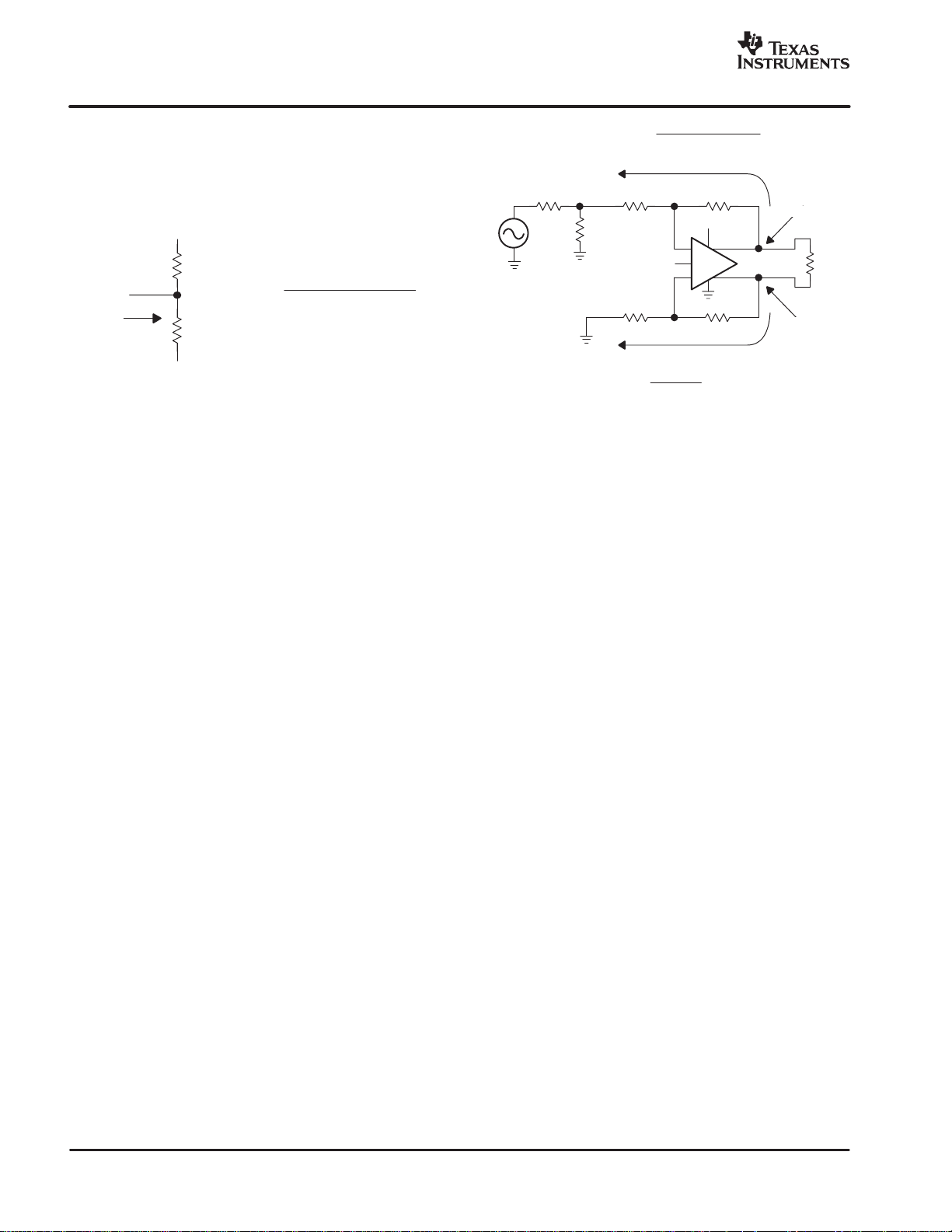
TERMINAL FUNCTIONS
Fully differential amplifiers are typically packaged in
eight-pin packages as shown in the diagram. The device
pins include two inputs (V
V
), two power supplies (VS+, VS−), an output
OUT+
common-mode control pin (V
power-down pin (PD).
V
1
IN−
V
V
OCM
V
S+
OUT+
2
3
4
Fully Differential Amplifier Pin Diagram
A standard configuration for the device is shown in the
figure. The functionality of a fully differential amplifier can
be imagined as two inverting amplifiers that share a
common noninverting terminal (though the voltage is not
necessarily fixed). For more information on the basic
theory of operation for fully differential amplifiers, refer to
the Texas Instruments application note titled Fully
Differential Amplifiers, literature number SLOA054.
INPUT COMMON-MODE VOLTAGE RANGE
AND THE THS4500 FAMILY
The key difference between the THS4500/1 and the
THS4502/3 is the input common-mode range for the two
devices. The input common-mode range of the
THS4504/5 is the same as the THS4500/1. The THS4502
and THS4503 have an input common-mode range that is
centered around midrail, and the THS4500 and THS4501
have an input common-mode range that is shifted to
include the negative power supply rail. Selection of one or
the other is determined by the nature of the application.
Specifically, the THS4500 and THS4501 are designed for
use in single-supply applications where the input signal is
ground-referenced, as depicted in Figure 75. The
THS4502 and THS4503 are designed for use in
single-supply or split-supply applications where the input
signal is centered between the power supply voltages, as
depicted in Figure 76.
IN+
, V
), two outputs (V
IN−
), and an optional
OCM
OUT−
V
8
IN+
7
PD
6
V
S−
V
5
OUT−
,
19
Page 20

V
(1–β)–V
(1–β))2V
V
2β
)
)
SLOS363A − AUGUST 2002 − REVISED AUGUST 2003
www.ti.com
R
S
V
S
Application Circuit for the THS4500 and THS4501,
Featuring Single-Supply Operation With a
Ground-Referenced Input Signal
R
g1
R
T
V
OCM
R
g2
R
f1
+V
S
+
−
+
−
R
f2
Figure 75
R
S
V
S
Application Circuit for the THS4500 and THS4501,
Featuring Split-Supply Operation With an Input
Signal Referenced at the Midrail
R
g1
R
T
V
OCM
R
g2
+V
+
−
−V
R
f1
S
−
+
S
R
f2
Figure 76
Equations 1−5 allow for calculation of the required input
common-mode range for a given set of input conditions.
The equations allow calculation of the input commonmode range requirements given information about the
input signal, the output voltage swing, the gain, and the
output common-mode voltage. Calculating the maximum
and minimum voltage required for VN and VP (the
amplifier’s input nodes) determines whether or not the
input common-mode range is violated or not. Four
equations are required. Two calculate the output voltages
and two calculate the node voltages at VN and VP (note
that only one of these needs calculation, as the amplifier
forces a virtual short between the two nodes).
V
OUT)
OUT–
+
+
–V
VN+ V
Where: β +
VP+ V
IN)
(1–β) ) V
IN)
(1–β) ) V
IN–
RF) R
(1–β) ) V
IN)
IN–
2β
(1–β)) 2V
IN–
β
OUT)
R
G
G
β
OUT–
OCM
β
OCM
(1
β
(2
(3)
(4)
(5)
NOTE:
The equations denote the device inputs as VN and
V
, and the circuit inputs as V
P
20
IN+
and V
IN−
.
R
V
IN+
V
IN−
Diagram For Input Common-Mode Range Equations
g
V
p
V
OCM
V
n
R
g
R
f
+
−
+
−
R
f
V
OUT−
V
OUT+
Figure 77
The two tables below depict the input common-mode
range requirements for two different input scenarios, an
input referenced around the negative rail and an input
referenced around midrail. The tables highlight the
differing requirements on input common-mode range, and
illustrate reasoning for choosing either the THS4500/1 or
the THS4502/3. For signals referenced around the
negative power supply, the THS4500/1 should be chosen
since its input common-mode range includes the negative
supply rail. For all other situations, the THS4502/3 offers
slightly improved distortion and noise performance for
applications with input signals centered between the
power supply rails.
Table 1. Negative-Rail Referenced
Gain
V
(V/V)
−2.0 to
1
−1.0 to
2
−0.5 to
4
−0.25 to
8
NOTE: This table assumes a negative-rail referenced, single-ended
input signal on a single 5-V supply as shown in Figure 75.
V
(V)
IN+
2.0
1.0
0.5
0.25
NMIN
V
V
IN
(VPP)
and V
V
NMAX
IN−
(V)
0 4 2.5 4 0.75 1.75
0 2 2.5 4 0.5 1.167
0 1 2.5 4 0.3 0.7
0 0.5 2.5 4 0.167 0.389
= V
PMIN
OCM
(V)
= V
V
OD
(VPP)
PMAX
V
NMIN
(V)
.
V
NMAX
(V)
Table 2. Midrail Referenced
Gain
V
(V/V)
1
2
4
2.25 to
8
NOTE: This table assumes a midrail referenced, single-ended input
signal on a single 5-V supply.
V
IN+
0.5 to
4.5
1.5 to
3.5
2.0 to
3.0
2.75
NMIN
V
V
IN
(VPP)
and V
V
NMAX
IN−
(V)
(V)
2.5 4 2.5 4 2 3
2.5 2 2.5 4 2.16 2.83
2.5 1 2.5 4 2.3 2.7
2.5 0.5 2.5 4 2.389 2.61
= V
PMIN
OCM
(V)
= V
V
OD
(VPP)
PMAX
V
.
NMIN
(V)
V
NMAX
(V)
Page 21

www.ti.com
R
1
R2
T
6)
R3)RT|| R
)
)
)
SLOS363A − AUGUST 2002 − REVISED AUGUST 2003
CHOOSING THE PROPER VALUE FOR THE
FEEDBACK AND GAIN RESISTORS
The selection of feedback and gain resistors impacts
circuit performance in a number of ways. The values in this
section provide the optimum high frequency performance
(lowest distortion, flat frequency response). Since the
THS4500 family of amplifiers is developed with a voltage
feedback architecture, the choice of resistor values does
not have a dominant effect on bandwidth, unlike a current
feedback amplifier. However, resistor choices do have
second-order effects. For optimal performance, the
following feedback resistor values are recommended. In
higher gain configurations (gain greater than two), the
feedback resistor values have much less ef fect on the high
frequency performance. Example feedback and gain
resistor values are given in the section on basic design
considerations (Table 3).
Amplifier loading, noise, and the flatness of the frequency
response are three design parameters that should be
considered when selecting feedback resistors. Larger
resistor values contribute more noise and can induce
peaking in the ac response in low gain configurations, and
smaller resistor values can load the amplifier more heavily,
resulting in a reduction in distortion performance. In
addition, feedback resistor values, coupled with gain
requirements, determine the value of the gain resistors,
directly impacting the input impedance of the entire circuit.
While there are no strict rules about resistor selection,
these trends can provide qualitative design guidance.
Table 3. Resistor Values for Balanced Operation
in Various Gain Configurations
V
OD
ǒ
Gain
V
1 392 412 383 54.9
1 499 523 487 53.6
2 392 215 187 60.4
2 1.3k 665 634 52.3
5 1.3k 274 249 56.2
5 3.32k 681 649 52.3
10 1.3k 147 118 64.9
10 6.81k 698 681 52.3
NOTE: Values in the table above assume a 50 Ω source impedance.
V
R2 & R4 (Ω) R1 (Ω) R3 (Ω) RT (Ω)
Ǔ
IN
R1
R
S
S
R3
R
T
R2
V
n
−
+
−
+
V
P
R4
V
out+
V
out−
V
OCM
Figure 78
Equations for calculating fully differential amplifier resistor
values in order to obtain balanced operation in the
presence of a 50-Ω source impedance are given in
equations 6 through 9.
APPLICATION CIRCUITS USING FULLY
DIFFERENTIAL AMPLIFIERS
Fully differential amplifiers provide designers with a great
deal of flexibility in a wide variety of applications. This
section provides an overview of some common circuit
configurations and gives some design guidelines.
Designing the interface to an ADC, driving lines
differentially, and filtering with fully differential amplifiers
are a few of the circuits that are covered.
BASIC DESIGN CONSIDERATIONS
The circuits in Figures 75 through 78 are used to highlight
basic design considerations for fully differential amplifier
circuit designs.
T
β1+
V
V
V
V
+
1
R
S
R1 ) R2
OD
+ 2
S
OD
+ 2
IN
–
R1
ǒ
1–
2(1)K)
1–β
ǒ
β1) β
1–β
β1) β
R3
β2+
K
2
Ǔǒ
2
2
Ǔ
2
K +
R1
R2 + R4
R3 + R1 *ǒRs|| R
S
R3 ) RT|| RS) R4
R
T
RT) R
Ǔ
S
(
Ǔ
(7
(8
(9
For more detailed information about balance in fully
differential amplifiers, see Fully Differential Amplifiers,
referenced at the end of this data sheet.
21
Page 22

C
SLOS363A − AUGUST 2002 − REVISED AUGUST 2003
www.ti.com
INTERFACING TO AN ANALOG-TO-DIGITAL
CONVERTER
The THS4500 family of amplifiers are designed
specifically to interface to today’s highest-performance
analog-to-digital converters. This section highlights the
key concerns when interfacing to an ADC and provides
example ADC/fully differential amplifier interface circuits.
Key design concerns when interfacing to an
analog-to-digital converter:
D Terminate the input source properly . In high-frequency
receiver chains, the source feeding the fully
differential amplifier requires a specific load
impedance (e.g., 50 Ω).
D Design a symmetric printed-circuit board layout.
Even-order distortion products are heavily influenced
by layout, and careful attention to a symmetric layout
will minimize these distortion products.
D Minimize inductance in power supply decoupling
traces and components. Poor power supply
decoupling can have a dramatic effect on circuit
performance. Since the outputs are differential,
differential currents exist in the power supply pins.
Thus, decoupling capacitors should be placed in a
manner that minimizes the impedance of the current
loop.
D Use separate analog and digital power supplies and
grounds. Noise (bounce) in the power supplies
(created by digital switching currents) can couple
directly into the signal path, and power supply noise
can create higher distortion products as well.
D Use care when filtering. While an RC low-pass filter
may be desirable on the output of the amplifier to filter
broadband noise, the excess loading can negatively
impact the amplifier linearity. Filtering in the feedback
path does not have this effect.
D AC-coupling allows easier circuit design. If
dc-coupling is required, be aware of the excess power
dissipation that can occur due to level-shifting the
output through the output common-mode voltage
control.
D Do not terminate the output unless required. Many
open-loop, class-A amplifiers require 50-Ω
termination for proper operation, but closed-loop fully
differential amplifiers drive a specific output voltage
regardless of the load impedance present.
Terminating the output of a fully differential amplifier
with a heavy load adversely effects the amplifier’s
linearity.
D Comprehend the V
Determine if t h e ADC’s voltage reference can provide
input drive requirements.
OCM
the required amount of current to move V
OCM
to the
desired value. A buffer may be needed.
D Decouple the V
effect. V
is a high-impedance node that can act as
OCM
pin to eliminate the antenna
OCM
an antenna. A large decoupling capacitor on this node
eliminates this problem.
D Be cognizant of the input common-mode range. If the
input signal is referenced around the negative power
supply rail (e.g., around ground on a single 5 V
supply), then the THS4500/1 accommodates the
input signal. If the input signal is referenced around
midrail, choose the THS4502/3 for the best operation.
D Packaging makes a difference at higher frequencies.
If possible, choose the smaller, thermally enhanced
MSOP package for the best performance. As a rule,
lower junction temperatures provide better
performance. If possible, use a thermally enhanced
package, even if the power dissipation is relatively
small compared to the maximum power dissipation
rating to achieve the best results.
D Comprehend the effect of the load impedance seen by
the fully differential amplifier when performing
system-level intercept point calculations. Lighter
loads (such as those presented by an ADC) allow
smaller intercept points to support the same level of
intermodulation distortion performance.
EXAMPLE ANALOG-TO-DIGITAL
CONVERTER DRIVER CIRCUITS
The THS4500 family of devices is designed to drive
high-performance ADCs with extremely high linearity,
allowing for the maximum effective number of bits at the
output of the data converter. Two representative circuits
shown below highlight single-supply operation and split
supply operation. Specific feedback resistor , gain resistor,
and feedback capacitor values are not specified, as their
values depend on the frequency of interest. Information on
calculating these values can be found in the applications
material above.
F
R
R
g
S
V
S
Using the THS4503 With the ADS5410
R
T
+
V
−
1 µF
R
−5 V
g
R
5 V
10 µF 0.1 µF
−
OCM
+
THS4503
10 µF 0.1 µF
R
Figure 79
f
iso
iso
5 V
IN
ADS5410
12 Bit/80 MSps
IN
CM
0.1 µF
R
R
f
C
F
22
Page 23

www.ti.com
C
C
F
R
R
g
S
V
S
R
T
+
V
−
1 µF
R
g
5 V
OCM
−
+
R
f
10 µF 0.1 µF
THS4501
R
f
C
F
R
iso
R
iso
5 V
ADS5421
IN
14 Bit/40 MSps
IN
CM
0.1 µF
Using the THS4501 With the ADS5421
Figure 80
FULLY DIFFERENTIAL LINE DRIVERS
The THS4500 family of amplifiers can be used as
high-frequency, high-swing differential line drivers. Their
high power supply voltage rating (16.5 V absolute
maximum) allows operation on a single 12-V or a single
15-V supply. The high supply voltage, coupled with the
ability to provide differential outputs enables the ability to
drive 26 VPP into reasonably heavy loads (250 Ω or
greater). The circuit in Figure 81 illustrates the THS4500
family of devices used as high speed line drivers. For line
driver applications, close attention must be paid to thermal
design constraints due to the typically high level of power
dissipation.
C
G
R
T
0.1 µF
R
g
V
OCM
R
R
S
V
S
g
R
f
15 V
+
−
THS4504 V
+
−
R
f
C
G
DD
R
iso
R
iso
VOD = 26 V
C
S
R
C
S
PP
Fully Differential Line Driver With High Output Swing
Figure 81
FILTERING WITH FULLY DIFFERENTIAL
AMPLIFIERS
Similar to their single-ended counterparts, fully differential
amplifiers have the ability to couple filtering functionality
with voltage gain. Numerous filter topologies can be based
on fully differential amplifiers. Several of these are outlined
in A Differential Circuit Collection, (literature number
SLOA064) referenced at the end of this data sheet. The
circuit below depicts a simple two-pole low-pass filter
SLOS363A − AUGUST 2002 − REVISED AUGUST 2003
applicable to many different types of systems. The first
pole is set by the resistors and capacitors in the feedback
paths, and the second pole is set by the isolation resistors
and the capacitor across the outputs of the isolation
resistors.
F1
R
S
V
S
R
g1
R
T
R
g2
A Two-Pole, Low-Pass Filter Design Using a Fully
Differential Amplifier With Poles Located at:
P1 = (2πRfCF)−1 in Hz and P2 = (4πR
Figure 82
Often times, filters like these are used to eliminate
broadband noise and out-of-band distortion products in
signal acquisition systems. It should be noted that the
increased load placed on the output of the amplifier by the
second low-pass filter has a detrimental effect on the
distortion performance. The preferred method of filtering
is using the feedback network, as the typically smaller
capacitances required at these points in the circuit do not
load the amplifier nearly as heavily in the pass-band.
SETTING THE OUTPUT COMMON-MODE
VOLTAGE WITH THE V
L
The output common-mode voltage pin provides a critical
function to the fully dif ferential amplifier; it accepts an input
voltage and reproduces that input voltage as the output
common-mode voltage. In other words, the V
provides the ability to level-shift the outputs to any voltage
inside the output voltage swing of the amplifier.
A description of the input circuitry of the V
below to facilitate an easier understanding of the V
interface requirements. The V
resistors between the power supply rails to set the default
output common-mode voltage to midrail. A voltage
applied to the V
voltage as long as the source has the ability to provide
enough current to overdrive the two 50-kΩ resistors. This
phenomenon is depicted in the V
diagram. The table contains some representative
examples to aid in determining the current drive
requirement for the V
is especially important when using the reference voltage
pin alters the output common-mode
OCM
voltage source. This parameter
OCM
+
−
OCM
OCM
R
f1
R
iso
−
+
R
iso
R
f2
C
F2
C)−1 in Hz
iso
INPUT
OCM
pin is shown
OCM
pin has two 50-kΩ
equivalent circuit
OCM
C
V
O
input
OCM
23
Page 24
V
V
SLOS363A − AUGUST 2002 − REVISED AUGUST 2003
www.ti.com
of an analog-to-digital converter to drive V
OCM
. Output
current drive capabilities differ from part to part, so a
voltage buffer may be necessary in some applications.
V
S+
R = 50 kΩ
V
OCM
I
IN
Equivalent Input Circuit for V
R = 50 kΩ
V
S−
IIN =
OCM
2 V
OCM
− VS+ − V
R
S−
Figure 83
I1 =
R
T
V
OCM
R
g1
= 2.5 V
R
g2
I2 =
Rf2 + R
R
S
S
Depiction of DC Power Dissipation Caused By
Output Level-Shifting in a DC-Coupled Circuit
OCM
Rf1+ Rg1 + RS || R
DC Current Path to Ground
5 V
+
−
DC Current Path to Ground
V
OCM
g2
T
R
f1
−
+
R
f2
2.5-V DC
R
2.5-V DC
L
Figure 84
By design, the input signal applied to the V
propagates to the outputs as a common-mode signal. As
shown in the equivalent circuit diagram, the V
has a high impedance associated with it, dictated by the
two 50-kΩ resistors. While the high impedance allows for
relaxed drive requirements, it also allows the pin and any
associated printed-circuit board traces to act as an
antenna. For this reason, a decoupling capacitor is
recommended o n this node for the sole purpose of filtering
any high frequency noise that could couple into the signal
path through the V
circuitry. A 0.1-µF or 1-µF
OCM
capacitance is a reasonable value for eliminating a great
deal of broadband interference, but additional, tuned
decoupling capacitors should be considered if a specific
source of electromagnetic or radio frequency interference
is present elsewhere in the system. Information on the ac
performance (bandwidth, slew rate) of the V
OCM
is included in the specification table and graph section.
OCM
input
OCM
circuitry
pin
SAVING POWER WITH POWER-DOWN
FUNCTIONALITY
The THS4500 family of fully differential amplifiers contains
devices that come with and without the power-down
option. Even-numbered devices have power-down
capability, which is described in detail here.
The power-down pin of the amplifiers defaults to the
positive supply voltage in the absence of an applied
voltage (i.e. an internal pullup resistor is present), putting
the amplifier in the power-on mode of operation. To turn off
the amplifier in an effort to conserve power, the
power-down pin can be driven towards the negative rail.
The threshold voltages for power-on and power-down are
relative to the supply rails and given in the specification
tables. Above the enable threshold voltage, the device is
on. Below the disable threshold voltage, the device is off.
Behavior in between these threshold voltages is not
specified.
Since the V
common-mode voltage, the ability for increased power
dissipation exi s t s . W h i l e t h i s does not pose a performance
problem for the amplifier, it can cause additional power
dissipation of which the system designer should be aware.
The circuit shown in Figure 84 demonstrates an example
of this phenomenon. For a device operating on a single
5-V supply with an input signal referenced around ground
and an output common-mode voltage of 2.5 V, a dc
potential exists between the outputs and the inputs of the
device. The amplifier sources current into the feedback
network in order to provide the circuit with the proper
operating point. While there are no serious effects on the
circuit performance, the extra power dissipation may need
to be included in the system’s power budget.
pin provides the ability to set an output
OCM
Note that this power-down functionality is just that; the
amplifier consumes less power in power-down mode. The
power-down mode is not intended to provide a
high-impedance output. In other words, the power-down
functionality is not intended to allow use as a 3-state bus
driver. When in power-down mode, the impedance looking
back into the output of the amplifier is dominated by the
feedback and gain setting resistors.
The time delays associated with turning the device on and
off are specified as the time it takes for the amplifier to
reach 50% of the nominal quiescent current. The time
delays are on the order of microseconds because the
amplifier moves in and out of the linear mode of operation
in these transitions.
24
Page 25

www.ti.com
SLOS363A − AUGUST 2002 − REVISED AUGUST 2003
LINEARITY: DEFINITIONS, TERMINOLOGY,
CIRCUIT TECHNIQUES, AND DESIGN
TRADEOFFS
The THS4500 family of devices features unprecedented
distortion performance for monolithic fully differential
amplifiers. This section focuses on the fundamentals of
distortion, circuit techniques for reducing nonlinearity,
and methods for equating distortion of fully differential
amplifiers to desired linearity specifications in RF receiver
chains.
Amplifiers are generally thought of as linear devices. In
other words, the output of an amplifier is a linearly scaled
version of the input signal applied to it. In reality, however,
amplifier transfer functions are nonlinear. Minimizing
amplifier nonlinearity is a primary design goal in many
applications.
Intercept points are specifications that have long been
used as key design criteria in the RF communications
world as a metric for the intermodulation distortion
performance of a device in the signal chain (e.g.,
amplifiers, mixers, etc.). Use of the intercept point, rather
than strictly the intermodulation distortion, allows for
simpler system-level calculations. Intercept points, like
noise figures, can be easily cascaded back and forth
through a signal chain to determine the overall receiver
chain’s intermodulation distortion performance. The
relationship between intermodulation distortion and
intercept point is depicted in Figure 85 and Figure 86.
P
∆fc = fc − f1
∆fc = f2 − f
Power
P
c
P
S
O
O
P
S
IMD3 = PS − P
O
P
OUT
(dBm)
OIP
P
O
P
S
3
IMD
3
IIP
3X
1X
3
P
IN
(dBm)
Figure 86
Due to the intercept point’s ease of use in system level
calculations for receiver chains, it has become the
specification of choice for guiding distortion-related design
decisions. Traditionally, these systems use primarily
class-A, single-ended RF amplifiers as gain blocks. These
RF amplifiers are typically designed to operate in a 50-Ω
environment, just like the rest of the receiver chain. Since
intercept points are given in dBm, this implies an
associated impedance (50 Ω).
However, with a fully differential amplifier , the output does
not require termination as an RF amplifier would. Because
closed-loop amplifiers deliver signals to their outputs
regardless of the impedance present, it is important to
comprehend this when evaluating the intercept point of a
fully differential amplifier. The THS4500 series of devices
yields optimum distortion performance when loaded with
200 Ω to 1 kΩ, very similar to the input impedance of an
analog-to-digital converter over its input frequency band.
As a result, terminating the input of the ADC to 50 Ω can
actually be detrimental to system performance.
This discontinuity between open-loop, class-A amplifiers
and closed-loop, class-AB amplifiers becomes apparent
when comparing the intercept points of the two types of
devices. Equation 10 gives the definition of an intercept
point, relative to the intermodulation distortion.
fc − 3∆ff1fcf2 fc + 3∆f
f − Frequency − MHz
Figure 85
Ť
Ť
IMD
3
ǒ
OIP3+ P
PO+ 10 log
NOTE: Po is the output power of a single tone, RL is the differential load
)
O
ǒ
resistance, and V
single tone.
Ǔ
where
2
2
V
Pdiff
2RL 0.001
is the differential peak voltage for a
P(diff)
Ǔ
(10)
(11)
25
Page 26

e
e
o
o
Ȣ
Ȥ
NA: Fully Differential Amplifier
)
)
4)
5)
6)
7)
SLOS363A − AUGUST 2002 − REVISED AUGUST 2003
www.ti.com
As can be seen in the equation, when a higher impedance
is used, the same level of intermodulation distortion
performance results in a lower intercept point. Therefore,
it is important to comprehend the impedance seen by the
output of the fully differential amplifier when selecting a
minimum intercept point. The graphic below shows the
relationship between the strict definition of an intercept
point with a normalized, or equivalent, intercept point for
the THS4502.
THIRD-ORDER OUTPUT INTERCEPT POINT
60
50
40
30
20
10
0
3
0 20 40 60 80 100
OIP − Third-Order Output Intersept Point − dBm
Comparing specifications between different device types
becomes easier when a common impedance level is
assumed. For this reason, the intercept points on the
THS4500 family of devices are reported normalized to a
50-Ω load impedance.
AN ANALYSIS OF NOISE IN FULLY
DIFFERENTIAL AMPLIFIERS
Noise analysis in fully differential amplifiers is analogous
to noise analysis in single-ended amplifiers. The same
concepts apply. Below, a generic circuit diagram
consisting of a voltage source, a termination resistor, two
gain setting resistors, two feedback resistors, and a fully
differential amplifier is shown, including all the relevant
noise sources. From this circuit, the noise factor (F) and
noise figure (NF) are calculated. The figures indicate the
appropriate scaling factor for each of the noise sources in
two different cases. The first case includes the termination
resistor, and the second, simplified case assumes that the
voltage source is properly terminated by the gain-setting
resistors. With these scaling factors, the amplifier’s input
noise power (NA) can be calculated by summing each
individual noise source with its scaling factor. The noise
FREQUENCY
Gain = 1
Rf = 499 Ω
VO = 2 V
VS = ± 5 V
200 kHz Tone Spacing
Normalized to 200 Ω
f − Frequency − MHz
Figure 87
vs
PP
Normalized to 50 Ω
RL = 800 Ω
delivered to the amplifier by the source (NI) and input noise
power are used to calculate the noise factor and noise
figure as shown in equations 23 through 27.
g
R
NiN
R
s
e
s
A
S
i
N
i
R
t
e
t
e
g
i
ni
ge
R
g
R
f
e
n
+
fully-diff
amp
−
i
ii
R
f
f
N
S
o
N
f
Figure 88. Noise Sources in a Fully
Differential Amplifier Circuit
Noise
Source
(eni)
(ini)
(iii)
4kTR
4kTR
4kTR
Figure 89. Scaling Factors for Individual Noise
Sources Assuming a Finite Value Termination
2
2
2
t
f
g
Scale Factor
ȡ
R
g
)
ȧ
R
f
R
R
2
g
2
g
R
2
t
g
2RsR
Rs)2R
2RsR
)
Rs)2R
R
ǒ
R
Ȣ
R
ȡ
ȧ
Ȣ
ȡ
2
ȧ
ȧ
R
)
g
R
)
2ǒRs)R
G
g
g
2
g
Ǔ
f
R
2ǒRs)R
ȣ
g
RsR
ȧ
t
Ǔ
t
Ȥ
2
ȣ
ȧ
Ȥ
g
g
RsR
t
t
Resistor
Ǔ
ȣ
ȧ
ȧ
2
(12
(13
(1
(1
(1
2
(1
26
Page 27

www.ti.com
Ȣ
Ȥ
NA: Fully Differential Amplifier; termination = 2R
)
)
)
)
)
SLOS363A − AUGUST 2002 − REVISED AUGUST 2003
Noise
Source
(eni)
(ini)
(iii)
4kTR
4kTR
Figure 90. Scaling Factors for Individual Noise
Sources Assuming No Termination Resistance is
Ni+ 4kTR
Ni+ 4kTR
Figure 92. Input Noise Assuming No Termination
Noise Factor and Noise Figure Calculations
N
NF + 10 log (F)
Scale Factor
R
ȡ
2
R
ȧ
Ȣ
2
R
g
R
2
g
2
f
2
g
ȡ
ȧ
ȧ
s
ȧ
ȧ
Ȣ
Figure 91. Input Noise With a Termination
ǒ
s
ǒ
+ S
Noise Source Scale Factor
A
F + 1 )
N
N
R
g
f
2
2
R
Rs) 2R
A
I
g
)
s
R
R
)
g
2
2
R
g
ǒ
Ǔ
R
f
R
g
ȡ
R
2RtR
2RtR
Rt)2R
2R
g
)
g
g
g
Ǔ
g
R
2
g
g
Resistor
2
Resistor
ȧ
Used (e.g., R
Rt)2R
)
ȣ
ȧ
s
Ȥ
ȣ
ȧ
s
ȣ
ȧ
ȧ
ȧ
ȧ
Ȥ
PRINTED-CIRCUIT BOARD LAYOUT
TECHNIQUES FOR OPTIMAL
PERFORMANCE
Achieving optimum performance with a high frequency
amplifier-like devices in the THS4500 family requires
careful attention to board layout parasitic and external
component types.
Recommendations that optimize performance include:
2
2
2
is open).
T
g
(18
(19
(20
(21
(22
D Minimize parasitic capacitance to any ac ground for all
of the signal I/O pins. Parasitic capacitance on the
output and input pins can cause instability. To reduce
unwanted capacitance, a window around the signal
I/O pins should be opened in all of the ground and
power planes around those pins. Otherwise, ground
and power planes should be unbroken elsewhere on
the board.
D Minimize the distance (< 0.25”) from the power supply
pins to high frequency 0.1-µF decoupling capacitors.
At the device pins, the ground and power plane layout
should not be in close proximity to the signal I/O pins.
Avoid narrow power and ground traces to minimize
inductance between the pins and the decoupling
capacitors. The power supply connections should
always be decoupled with these capacitors. Larger
(6.8 µF or more) tantalum decoupling capacitors,
effective at lower frequency, should also be used on
the main supply pins. These may be placed somewhat
farther from the device and may be shared among
several devices in the same area of the PC board. The
primary goal is to minimize the impedance seen in the
differential-current return paths.
D Careful selection and placement of external
(23)
(24)
Ǔ
(25)
(26)
(27)
components preserve the high frequency
performance o f the THS4500 family. Resistors should
be a very low reactance type. Surface-mount resistors
work best and allow a tighter overall layout. Metal-film
and carbon composition, axially-leaded resistors can
also provide good high frequency performance.
Again, keep their leads and PC board trace length as
short as p o s s i b l e . Never use wirewound type resistors
in a high frequency application. Since the output pin
and inverting input pins are the most sensitive to
parasitic capacitance, always position the feedback
and series output resistors, if any, as close as possible
to the inverting input pins and output pins. Other
network components, such as input termination
resistors, should be placed close to the gain-setting
resistors. Even with a low parasitic capacitance
shunting the external resistors, excessively high
resistor values can create significant time constants
that can degrade performance. Good axial metal-film
or surface-mount resistors have approximately 0.2 pF
in shunt with the resistor. For resistor values > 2 .0kΩ,
this parasitic capacitance can add a pole and/or a zero
below 400 MHz that can effect circuit operation. Keep
resistor values as low as possible, consistent with
load driving considerations.
D Connections to other wideband devices on the board
may be made with short direct traces or through
onboard transmission lines. For short connections,
consider the trace and the input to the next device as
a lumped capacitive load. Relatively wide traces
(50 mils to 100 mils) should be used, preferably with
27
Page 28

4
SLOS363A − AUGUST 2002 − REVISED AUGUST 2003
www.ti.com
ground and power planes opened up around them.
Estimate the total capacitive load and determine if
isolation resistors on the outputs are necessary. Low
parasitic capacitive loads (< 4 pF) may not need an R
since the THS4500 family is nominally compensated
to operate with a 2-pF parasitic load. Higher parasitic
capacitive loads without an RS are allowed as the
signal gain increases (increasing the unloaded phase
margin). If a long trace is required, and the 6-dB signal
loss intrinsic to a doubly-terminated transmission line
is acceptable, implement a matched impedance
transmission line using microstrip or stripline
techniques (consult an ECL design handbook for
microstrip and stripline layout techniques).
A 50-Ω environment is normally not necessary
onboard, and in fact, a higher impedance environment
improves distortion as shown in the distortion versus
load plots. With a characteristic board trace
impedance defined based on board material and trace
dimensions, a matching series resistor into the trace
from the output of the THS4500 family is used as well
as a terminating shunt resistor at the input of the
destination device.
Remember also that the terminating impedance is t h e
parallel combination of the shunt resistor and the input
impedance of the destination device: this total
effective impedance should be set to match the trace
impedance. If the 6-dB attenuation of a doubly
terminated transmission line is unacceptable, a long
trace can be series-terminated at the source end only.
Treat the trace as a capacitive load in this case. This
does not preserve signal integrity as well as a
doubly-terminated line. If the input impedance of the
destination device is low, there is some signal
attenuation due to the voltage divider formed by the
series output into the terminating impedance.
D Socketing a high speed part like the THS4500 family
is not recommended. The additional lead length and
pin-to-pin capacitance introduced by the socket can
create an extremely troublesome parasitic network
which can make it almost impossible to achieve a
smooth, stable frequency response. Best results are
obtained by soldering the THS4500 family parts
directly onto the board.
PowerPAD DESIGN CONSIDERATIONS
The THS4500 family is available in a thermally-enhanced
PowerPAD family of packages. These packages are
S
constructed using a downset leadframe upon which the die
is mounted [see Figure 93(a) and Figure 93(b)]. This
arrangement results in the lead frame being exposed as a
thermal pad on the underside of the package [see
Figure 93(c)]. Because this thermal pad has direct thermal
contact with the die, excellent thermal performance can be
achieved by providing a good thermal path away from the
thermal pad.
The PowerPAD package allows for both assembly and
thermal management in one manufacturing operation.
During the surface-mount solder operation (when the
leads are being soldered), the thermal pad can also be
soldered to a copper area underneath the package.
Through the use of thermal paths within this copper area,
heat can be conducted away from the package into either
a ground plane or other heat dissipating device.
The PowerPAD package represents a breakthrough in
combining the small area and ease of assembly of surface
mount with the, heretofore, awkward mechanical methods
of heatsinking.
DIE
Side View (a)
DIE
End View (b)
Figure 93. Views of Thermally Enhanced
Package
Although there are many ways to properly heatsink the
PowerPAD package, the following steps illustrate the
recommended approach.
0.205
0.060
Pin 1
0.030
0.075 0.025
0.013
Bottom View (c)
Thermal
Pad
0.017
0.09
28
0.010
vias
Figure 94. Views of Thermally Enhanced
0.035
Top View
0.040
Package
Page 29

www.ti.com
T
–T
).
)
SLOS363A − AUGUST 2002 − REVISED AUGUST 2003
PowerPAD PCB LAYOUT CONSIDERATIONS
1. Prepare the PCB with a top side etch pattern as shown
in Figure 94. There should be etch for the leads as well
as etch for the thermal pad.
2. Place five holes in the area of the thermal pad. These
holes should be 13 mils in diameter. Keep them small
so that solder wicking through the holes is not a
problem during reflow.
3. Additional vias may be placed anywhere along the
thermal plane outside of the thermal pad area. This
helps dissipate the heat generated by the THS4500
family IC. These additional vias may be larger than the
13-mil diameter vias directly under the thermal pad.
They can be larger because they are not in the thermal
pad area to be soldered so that wicking is not a
problem.
4. Connect all holes to the internal ground plane.
5. When connecting these holes to the ground plane, do
not use the typical web or spoke via connection
methodology. Web connections have a high thermal
resistance connection that is useful for slowing the
heat transfer during soldering operations. This makes
the soldering of vias that have plane connections
easier. In this application, however, low thermal
resistance is desired for the most efficient heat
transfer. Therefore, the holes under the THS4500
family PowerPAD package should make their
connection to the internal ground plane with a
complete connection around the entire circumference
of the plated-through hole.
6. The top-side solder mask should leave the terminals
of the package and the thermal pad area with its five
holes exposed. The bottom-side solder mask should
cover the five holes of the thermal pad area. This
prevents solder from being pulled away from the
thermal pad area during the reflow process.
7. Apply solder paste to the exposed thermal pad area
and all of the IC terminals.
8. With these preparatory steps in place, the IC is simply
placed in position and run through the solder reflow
operation as any standard surface-mount
component. This results in a part that is properly
installed.
POWER DISSIPATION AND THERMAL
CONSIDERATIONS
The THS4500 family of devices does not incorporate
automatic thermal shutof f protection, so the designer must
take care to ensure that the design does not violate the
absolute maximum junction temperature of the device.
Failure may result if the absolute maximum junction
temperature o f 1 5 0 °C is exceeded. For best performance,
design for a maximum junction temperature of 125°C.
Between 125°C and 150°C, damage does not occur, but
the performance of the amplifier begins to degrade.
The thermal characteristics of the device are dictated by
the package and the PC board. Maximum power
dissipation for a given package can be calculated using the
following formula.
max
CA
A
q
JA
P
+
Dmax
Where:
is the maximum power dissipation in the amplifier (W
P
Dmax
T
is the absolute maximum junction temperature (°C).
max
TA is the ambient temperature (°C).
= θJC + θ
θ
JA
θJC is the thermal coefficient from the silicon junctions to the
case (°C/W).
is the thermal coefficient from the case to ambient air
θ
CA
(°C/W).
(28
For systems where heat dissipation is more critical, the
THS4500 family of devices is offered in an 8-pin MSOP
with PowerPAD. The thermal coefficient for the MSOP
PowerPAD package is substantially improved over the
traditional SOIC. Maximum power dissipation levels are
depicted in the graph for the two packages. The data for
the DGN package assumes a board layout that follows the
PowerPAD layout guidelines referenced above and
detailed in the PowerPAD application notes in the
Additional Reference Material section at the end of the
data sheet.
3.5
3
2.5
2
1.5
1
− Maximum Power Dissipation − W
0.5
D
P
0
−40 −20 0 20
θJA = 170°C/W for 8-Pin SOIC (D)
θJA = 58.4°C/W for 8-Pin MSOP (DGN)
ΤJ = 150°C, No Airflow
8-Pin DGN Package
8-Pin D Package
40 60 80
TA − Ambient Temperature − °C
Figure 95. Maximum Power Dissipation vs
Ambient Temperature
When determining whether or not the device satisfies the
maximum power dissipation requirement, it is important to
not only consider quiescent power dissipation, but also
dynamic power dissipation. Often times, this is difficult to
quantify because the signal pattern is inconsistent, but an
estimate of the RMS power dissipation can provide
visibility into a possible problem.
29
Page 30

SLOS363A − AUGUST 2002 − REVISED AUGUST 2003
www.ti.com
DRIVING CAPACITIVE LOADS
High-speed amplifiers are typically not well-suited for
driving large capacitive loads. If necessary, however , t he
load capacitance should be isolated by two isolation
resistors in series with the output. The requisite isolation
resistor size depends on the value of the capacitance, but
10 to 25 Ω is a good place to begin the optimization
process. Larger isolation resistors decrease the amount of
peaking in the frequency response induced by the
capacitive load, but this comes at the expense of larger
voltage drop across the resistors, increasing the output
swing requirements of the system.
R
f
V
+
−
−V
S
−
+
S
R
R
iso
C
L
R
iso
Riso = 10 − 25 Ω
f
R
S
V
S
R
g
R
T
R
g
Use of Isolation Resistors With a Capacitive Load.
Figure 96
POWER SUPPLY DECOUPLING
TECHNIQUES AND RECOMMENDATIONS
Power supply decoupling is a critical aspect of any
high-performance amplifier design process. Careful
decoupling provides higher quality ac performance (most
notably improved distortion performance). The following
guidelines ensure the highest level of performance.
1. Place decoupling capacitors as close to the power
supply inputs as possible, with the goal of minimizing
the inductance of the path from ground to the power
supply.
2. Placement priority should be as follows: smaller
capacitors should be closer to the device.
3. Use of solid power and ground planes is
recommended to reduce the inductance along power
supply return current paths.
4. Recommended values for power supply decoupling
include 10-µF and 0.1-µF capacitors for each supply.
A 1000-pF capacitor can be used across the supplies
as well for extremely high frequency return currents,
but often is not required.
EVALUATION FIXTURES, SPICE MODELS,
AND APPLICATIONS SUPPORT
Texas Instruments is committed to providing its customers
with the highest quality of applications support. To support
this goal, an evaluation board has been developed for the
THS4500 family of fully differential amplifiers. The
evaluation board can be obtained by ordering through the
Texas Instruments web site, www.ti.com, or through your
local Texas Instruments sales representative. Schematic
for the evaluation board is shown below with their default
component values. Unpopulated footprints are shown to
provide insight into design flexibility.
C4
C0805
R4
R0805
PD
V
S
J1
R1
C0805
R1206
C0805
C1
R2
R0805
C2
R0805
R3
U1
THS450X
3
7
1
_
8
+
6
2
−V
S
V
OCM
R5
C3
J2
R0805
J3
PwrPad
R0805
C0805
R0805
4
5
R8
R0805
R9
R6
R0805
R0805
R7
R9
C0805
5
6
Simplified Schematic of the Evaluation Board. Power
Supply Decoupling, V
Not Shown
and Power Down Circuitry
OCM,
Figure 97
Computer simulation of circuit performance using SPICE
is often useful when analyzing the performance of analog
circuits and systems. This is particularly true for video and
RF amplifier circuits where parasitic capacitance and
inductance can have a major ef fect o n circuit performance.
A SPICE model for the THS4500 family of devices is
available through either the Texas Instruments web site
(www.ti.com) or as one model on a disk from the Texas
Instruments Product Information Center
(1−800−548−6132). The PIC is also available for design
assistance and detailed product information at this
number. These models do a good job of predicting
small-signal ac and transient performance under a wide
variety of operating conditions. They are not intended to
model the distortion characteristics of the amplifier, nor d o
they attempt to distinguish between the package types in
their small-signal ac performance. Detailed information
about what is and is not modeled is contained in the model
file itself.
C0805
C7
T1
C5
C6
C0805
314
J2
J3
R11
R1206
J2
J3
J4
30
Page 31

www.ti.com
SLOS363A − AUGUST 2002 − REVISED AUGUST 2003
ADDITIONAL REFERENCE MATERIAL
D PowerPAD Made Easy, application brief, Texas Instruments Literature Number SLMA004.
D PowerPAD Thermally Enhanced Package, technical brief, Texas Instruments Literature Number SLMA002.
D Karki, James. Fully Differential Amplifiers. application report, Texas Instruments Literature Number SLOA054D.
D Karki, James. Fully Differential Amplifiers Applications: Line Termination, Driving High−Speed ADCs, and Differential
Transmission Lines. Texas Instruments Analog Applications Journal, February 2001.
D Carter, Bruce. A Differential Op-Amp Circuit Collection. application report, Texas Instruments Literature Number
SLOA064.
D Carter, Bruce. Differential Op-Amp Single-Supply Design Technique, application report, Texas Instruments Literature
Number SLOA072.
D Karki, James. Designing for Low Distortion with High-Speed Op Amps. Texas Instruments Analog Applications
Journal, July 2001.
31
Page 32

Page 33

MECHANICAL DATA
MSOI002B – JANUARY 1995 – REVISED SEPTEMBER 2001
D (R-PDSO-G**) PLASTIC SMALL-OUTLINE PACKAGE
8 PINS SHOWN
8 5
1 4
A
0.069 (1,75) MAX
0.020 (0,51)
0.014 (0,35)
0.157 (4,00)
0.150 (3,81)
0.010 (0,25)
0.004 (0,10)
0.244 (6,20)
0.228 (5,80)
0.010 (0,25)0.050 (1,27)
0.008 (0,20) NOM
Gage Plane
0.010 (0,25)
0°– 8°
0.044 (1,12)
0.016 (0,40)
Seating Plane
0.004 (0,10)
PINS **
DIM
A MAX
A MIN
NOTES: A. All linear dimensions are in inches (millimeters).
B. This drawing is subject to change without notice.
C. Body dimensions do not include mold flash or protrusion, not to exceed 0.006 (0,15).
D. Falls within JEDEC MS-012
8
0.197
(5,00)
0.189
(4,80)
14
0.344
(8,75)
0.337
(8,55)
16
0.394
(10,00)
0.386
(9,80)
4040047/E 09/01
POST OFFICE BOX 655303 • DALLAS, TEXAS 75265
1
Page 34

IMPORTANT NOTICE
Texas Instruments Incorporated and its subsidiaries (TI) reserve the right to make corrections, modifications,
enhancements, improvements, and other changes to its products and services at any time and to discontinue
any product or service without notice. Customers should obtain the latest relevant information before placing
orders and should verify that such information is current and complete. All products are sold subject to TI’s terms
and conditions of sale supplied at the time of order acknowledgment.
TI warrants performance of its hardware products to the specifications applicable at the time of sale in
accordance with TI’s standard warranty . Testing and other quality control techniques are used to the extent TI
deems necessary to support this warranty . Except where mandated by government requirements, testing of all
parameters of each product is not necessarily performed.
TI assumes no liability for applications assistance or customer product design. Customers are responsible for
their products and applications using TI components. T o minimize the risks associated with customer products
and applications, customers should provide adequate design and operating safeguards.
TI does not warrant or represent that any license, either express or implied, is granted under any TI patent right,
copyright, mask work right, or other TI intellectual property right relating to any combination, machine, or process
in which TI products or services are used. Information published by TI regarding third-party products or services
does not constitute a license from TI to use such products or services or a warranty or endorsement thereof.
Use of such information may require a license from a third party under the patents or other intellectual property
of the third party , or a license from TI under the patents or other intellectual property of TI.
Reproduction of information in TI data books or data sheets is permissible only if reproduction is without
alteration and is accompanied by all associated warranties, conditions, limitations, and notices. Reproduction
of this information with alteration is an unfair and deceptive business practice. TI is not responsible or liable for
such altered documentation.
Resale of TI products or services with statements different from or beyond the parameters stated by TI for that
product or service voids all express and any implied warranties for the associated TI product or service and
is an unfair and deceptive business practice. TI is not responsible or liable for any such statements.
Following are URLs where you can obtain information on other Texas Instruments products and application
solutions:
Products Applications
Amplifiers amplifier.ti.com Audio www.ti.com/audio
Data Converters dataconverter.ti.com Automotive www.ti.com/automotive
DSP dsp.ti.com Broadband www.ti.com/broadband
Interface interface.ti.com Digital Control www.ti.com/digitalcontrol
Logic logic.ti.com Military www.ti.com/military
Power Mgmt power.ti.com Optical Networking www.ti.com/opticalnetwork
Microcontrollers microcontroller.ti.com Security www.ti.com/security
Telephony www.ti.com/telephony
Video & Imaging www.ti.com/video
Wireless www.ti.com/wireless
Mailing Address: Texas Instruments
Post Office Box 655303 Dallas, Texas 75265
Copyright 2003, Texas Instruments Incorporated
 Loading...