

Page 1
www.ti.com
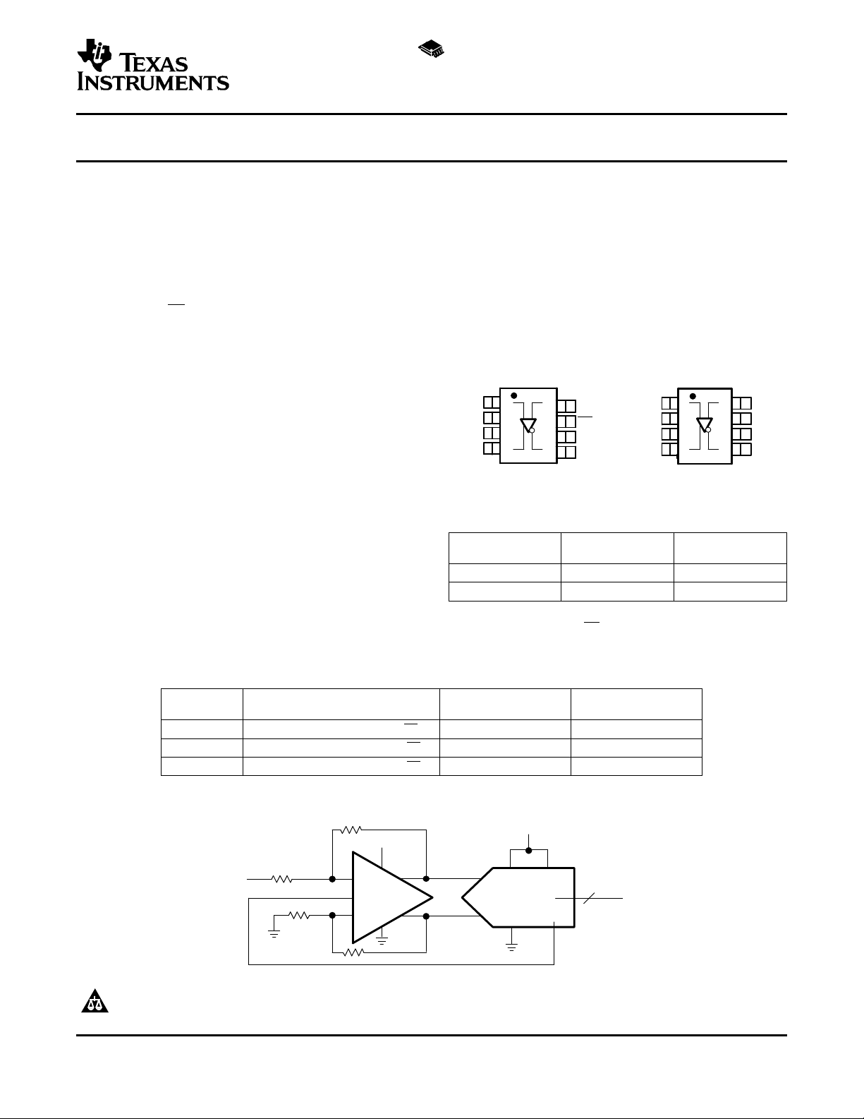
THS4121
D, DGN, OR DGK PACKAGE
(TOP VIEW)
1
2
3
4
8
7
6
5
V
IN−
V
OCM
V
DD
V
OUT+
V
IN+
NC
GND
V
OUT−
THS4120
D, DGN, OR DGK PACKAGE
(TOP VIEW)
1
2
3
4
8
7
6
5
V
IN−
V
OCM
V
DD
V
OUT+
V
IN+
PD
GND
V
OUT−
+
DIGITAL
OUTPUT
V
IN
−
+ −
DV
DD
V
OCM
AV
SS
AV
DD
A
IN
A
IN
V
DD
V
ref
3.3 V
TYPICAL A/D APPLICATION CIRCUIT
HIGH-SPEED FULLY DIFFERENTIAL I/O AMPLIFIERS
FEATURES KEY APPLICATIONS
• High Performance
– 100 MHz, –3 dB Bandwidth
– 50 V/µs Slew Rate
– 75 dB Total Harmonic Distortion at 1 MHz
(V
= 2 V
O
– 5.4 nV/ √ Hz Input-Referred Noise (10 kHz)
• Differential Input/Differential Output
– Balanced Outputs Reject Common-Mode
Noise
– Differential Reduced Second Harmonic
Distortion
• Power Supply Range
– V
= 3.3 V
DD
)
PP
THS4120
THS4121
SLOS319D – FEBRUARY 2001 – REVISED OCTOBER 2004
• Simple Single-Ended To Differential
Conversion
• Differential ADC Driver/Differential
Antialiasing
• Differential Transmitter and Receiver
• Output Level Shifter
DESCRIPTION
The THS412x is one in a family of fully differential-input, differential-output devices fabricated using
Texas Instruments' state-of-the-art submicron CMOS
process.
The THS412x consists of a true fully-differential
signal path from input to output. This results in THS4121 1 –
excellent common-mode noise rejection and
improved total harmonic distortion.
RELATED DEVICES
DEVICE
(1) See the TI Web site for additional high-speed amplifier devices.
(1)
THS413x 150 MHz, 51 V/µs, 1.3 nV/ √ Hz 5 V to 30 V ± 2.5 to ± 15
THS414x 160 MHz, 450 V/µs, 6.5 nV/ √ Hz 5 V to 30 V ± 2.5 to ± 15
THS415x 150 MHz, 650 V/µs, 7.6 nV/ √ Hz 5 V to 30 V ± 2.5 to ± 15
DESCRIPTION
HIGH-SPEED DIFFERENTIAL I/O FAMILY
DEVICE POWERDOWN
THS4120
(1) For proper functiionality, an external 10-k Ω pullup resistor is
required between the PD pin and the positive supply.
SINGLE SUPPLY SPLIT SUPPLY
VOLTAGE RANGE VOLTAGE RANGE
(1)
NUMBER OF
CHANNELS
1 Yes
Please be aware that an important notice concerning availability, standard warranty, and use in critical applications of Texas
Instruments semiconductor products and disclaimers thereto appears at the end of this data sheet.
PowerPAD is a trademark of Texas Instruments.
PRODUCTION DATA information is current as of publication date.
Products conform to specifications per the terms of the Texas
Instruments standard warranty. Production processing does not
necessarily include testing of all parameters.
Copyright © 2001–2004, Texas Instruments Incorporated
Page 2
www.ti.com
THS4120
THS4121
SLOS319D – FEBRUARY 2001 – REVISED OCTOBER 2004
These devices have limited built-in ESD protection. The leads should be shorted together or the device
placed in conductive foam during storage or handling to prevent electrostatic damage to the MOS gates.
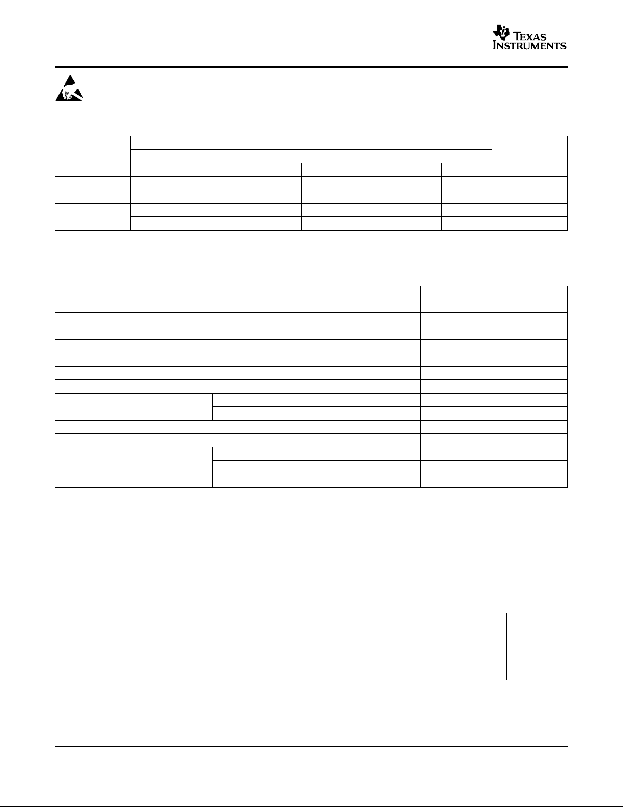
AVAILABLE OPTIONS
PACKAGED DEVICES
T
A
0 ° C to 70 ° C
–40 ° C to 85 ° C
SMALL OUTLINE(D)
THS4120CD THS4120CDGN ARL THS4120CDGK ATZ THS4120EVM
THS4121CD THS4121CDGN ASB THS4121CDGK ATO THS4121EVM
THS4120ID THS4120IDGN ARM THS4120IDGK ARN –
THS4121ID THS4121IDGN ASC THS4121IDGK ASN –
MSOP PowerPAD™ MSOP
(DGN) SYMBOL (DGK) SYMBOL
ABSOLUTE MAXIMUM RATINGS
over operating free-air temperature range (unless otherwise noted)
Supply voltage, GND to V
V
Input voltage ± V
I
I
Output current (sink)
O
V
Differential input voltage ± V
ID
Continuous total power dissipation See Dissipation Rating Table
T
Maximum junction temperature
J
T
Maximum junction temperature, continuous operation, long-term reliability
J
T
Operating free-air temperature
A
T
Storage Temperature –65 ° C to 150 ° C
stg
Lead temperature 1,6 mm (1/16 Inch) from case for 10 seconds 300 ° C
ESD ratings CDM 1500 V
(1) Stresses beyond those listed under "absolute maximum ratings” may cause permanent damage to the device. These are stress ratings
only, and functional operation of the device at these or any other conditions beyond those indicated under "recommended operating
conditions” is not implied. Exposure to absolute-maximum-rated conditions for extended periods may affect device reliability.
(2) The THS412x may incorporate a PowerPad™ on the underside of the chip. This acts as a heatsink and must be connected to a
thermally dissipative plane for proper power dissipation. Failure to do so may result in exceeding the maximum junction temperature
which could permanently damage the device. See TI technical brief SLMA002 and SLMA004 for more information about utilizing the
PowerPad™ thermally enhanced package.
(3) The absolute maximum temperature under any condition is limited by the constraints of the silicon process.
(4) The maximum junction temperature for continuous operation is limited by package constraints. Operation above this temperature may
result in reduced reliability and/or lifetime of the device.
DD
(2)
(3)
C suffix 0 ° C to 70 ° C
I suffix –40 ° C to 85 ° C
HBM 4000 V
MM 200 V
(1)
(4)
EVALUATION
MODULES
UNIT
3.6 V
DD
110 mA
DD
150 ° C
125 ° C
DISSIPATION RATING TABLE
PACKAGE θ
(1)
( ° C/W) θJC( ° C/W)
JA
POWER RATING
TA= 25 ° C TA= 85 ° C
D 97.5 38.3 1.02 W 410 mW
DGN 58.4 4.7 1.71 W 685 mW
DGK 260 54.2 385 mW 154 mW
(1) This data was taken using the JEDEC standard High-K test PCB.
(2) Power rating is determined with a junction temperature of 125 ° C. This is the point where distortion
starts to substantially increase. Thermal management of the final PCB should strive to keep the
junction temperature at or below 125 ° C for best performance and long-term reliability.
2
(2)
Page 3
www.ti.com
RECOMMENDED OPERATING CONDITIONS
V
T
Supply voltage V
DD
Operating free-air temperature ° C
A
Split supply ± 1.5 ± 1.65 ± 1.75
Single supply 3 3.3 3.5
C suffix 0 70
I suffix –40 85
ELECTRICAL CHARACTERISTICS
V
= 3.3 V, RL= 800 Ω , TA= 25 ° C (unless otherwise noted)
DD
PARAMETER TEST CONDITIONS MIN TYP MAX UNIT
DYNAMIC PERFORMANCE
BW Small-signal bandwidth (–3 dB) V
SR Slew rate
t
s
Settling time to 0.1% 60
Settling time to 0.01% 292
(2)
DISTORTION PERFORMANCE
Total harmonic distortion
THD Differential input, differential output V
Gain = 1, Rf= 200 Ω , RL= 800 Ω , VO= 2 V
PP
Total harmonic distortion
THD Differential input, differential output V
Gain = 1, Rf= 200 Ω , RL= 800 Ω , VO= 4 V
PP
Spurious free dynamic range (SFDR)
Differential input, differential output, VO= 4 V
PP
Third intermodulation distortion VI= 0.071 V
NOISE PERFORMANCE
V
I
n
Input voltage noise f = 10 kHz 5.4 nV/ √ Hz
n
Input current noise f = 10 kHz 1 fA/ √ Hz
DC PERFORMANCE
Open-loop gain dB
Input offset voltage
V
S
Input offset voltage, referred to V
OCM
Offset voltage drift TA= full range 25 µV/ ° C
I
IB
I
OS
Input bias current 1.2 pA
Input offset current 100 fA
Current offset drift TA= full range 5 fA/ ° C
(1) The full range temperature is 0 ° C to 70 ° C for the C suffix, and –40 ° C to 85 ° C for the I suffix.
(2) Slew rate is measured differentially from an output level range of 25% to 75%.
(1)
= 3.3 V, Gain = 1, Rf= 200 Ω 100 MHz
DD
V
= 3.3 V, Gain = 1 55 V/µs
DD
Differential step voltage = 2 VPP, Gain = 1 ns
= 3.3 V, f = 1 MHz –75 dB
DD
= 3.3 V, f = 1 MHz –66 dB
DD
Rf= 200 Ω , f = 1 MHz –69 dB
RMS
TA= 25 ° C 60 66
TA= full range 66
TA= 25 ° C 3 8
TA= full range 4 9
TA= 25 ° C 5 13
TA= full range 14
TA= full range
THS4120
THS4121
SLOS319D – FEBRUARY 2001 – REVISED OCTOBER 2004
MIN TYP MAX UNIT
Gain = 1, f = 10 MHz –75 dBc
mV
3
Page 4
www.ti.com
THS4120
THS4121
SLOS319D – FEBRUARY 2001 – REVISED OCTOBER 2004
ELECTRICAL CHARACTERISTICS (Continued)
V
= 3.3 V, RL= 800 Ω , TA= 25 ° C (unless otherwise noted)
DD
PARAMETER TEST CONDITIONS MIN TYP MAX UNIT
INPUT CHARACTERISTICS
CMRR Common-mode rejection ratio TA= full range 64 96 dB
V
r
C
r
Common-mode input voltage range TA= full range to V
ICR
Input resistance (dc level) Measured into each input terminal 820 M Ω
i
Input capacitance, closed loop 3 pF
i
Output resistance See Figure 16 1 Ω
o
OUTPUT CHARACTERISTICS
V
V
I
I
High-level output Voltage VIC= VDD/2, V
OH
Low-level output Voltage VIC= VDD/2, V
OL
Output current (sink), RL= 7 Ω V
O
Output current (source), RL= 7 Ω V
O
= 3.3 V, TA= 25 ° C 80 100 mA
DD
= 3.3 V, TA= 25 ° C 20 25 mA
DD
POWER SUPPLY
V
I
Supply voltage range Single supply 3.3 V
DD
Quiescent current (per amplifier) V
DD
= 3.3 V mA
DD
PSRR Power supply rejection ratio TA= 25 ° C 68 85 dB
POWER-DOWN CHARACTERISTICS (THS4120 ONLY)
Power-down voltage level
(2)
Power-down quiescent current µA
t
t
z
Turn-on time delay 4.8 µs
on
Turn-off time delay 3 ns
off
Output impedance f = 1 MHz 1 k Ω
o
Enable >1.4
Power-down <1.2
TA= 25 ° C 120
TA= full range 130
50% of final supply current value
(1)
0.65 to
V
- 0.1
DD
= 3.3 V, TA= 25 ° C 3.05 3.15 V
DD
= 3.3 V, TA= 25 ° C 0.25 0.15 V
DD
0.35
V
DD
TA= 25 ° C 11 13.5
TA= full range 16
V
(1) The full range temperature is 0 ° C to 70 ° C for the C suffix, and –40 ° C to 85 ° C for the I suffix.
(2) For detail information on the power-down circuit, see the power-down section in the application section of this data sheet.
4
Page 5
www.ti.com
−1.5
−1
−0.5
0
0.5
1
1.5
0 20 40 60 80
t − Time − ns
VDD = 3.3 V ,
VO = 2 VPP,
TA= 25°C
G = 1
RL = 800 Ω
− Output Voltage − VV
O
Rising Edge
Falling Edge
−4
−2
−1
0
1
2
100 k 1M 10 M 100 M 1G
G = 1
VI = 22.5 mV
RMS
VDD = 3.3 V
Rf = 270 Ω
Rf = 200 Ω
Gain − dB
f − Frequency − Hz
Rf = 390 Ω
Rf = 150 Ω
−3
SLOS319D – FEBRUARY 2001 – REVISED OCTOBER 2004
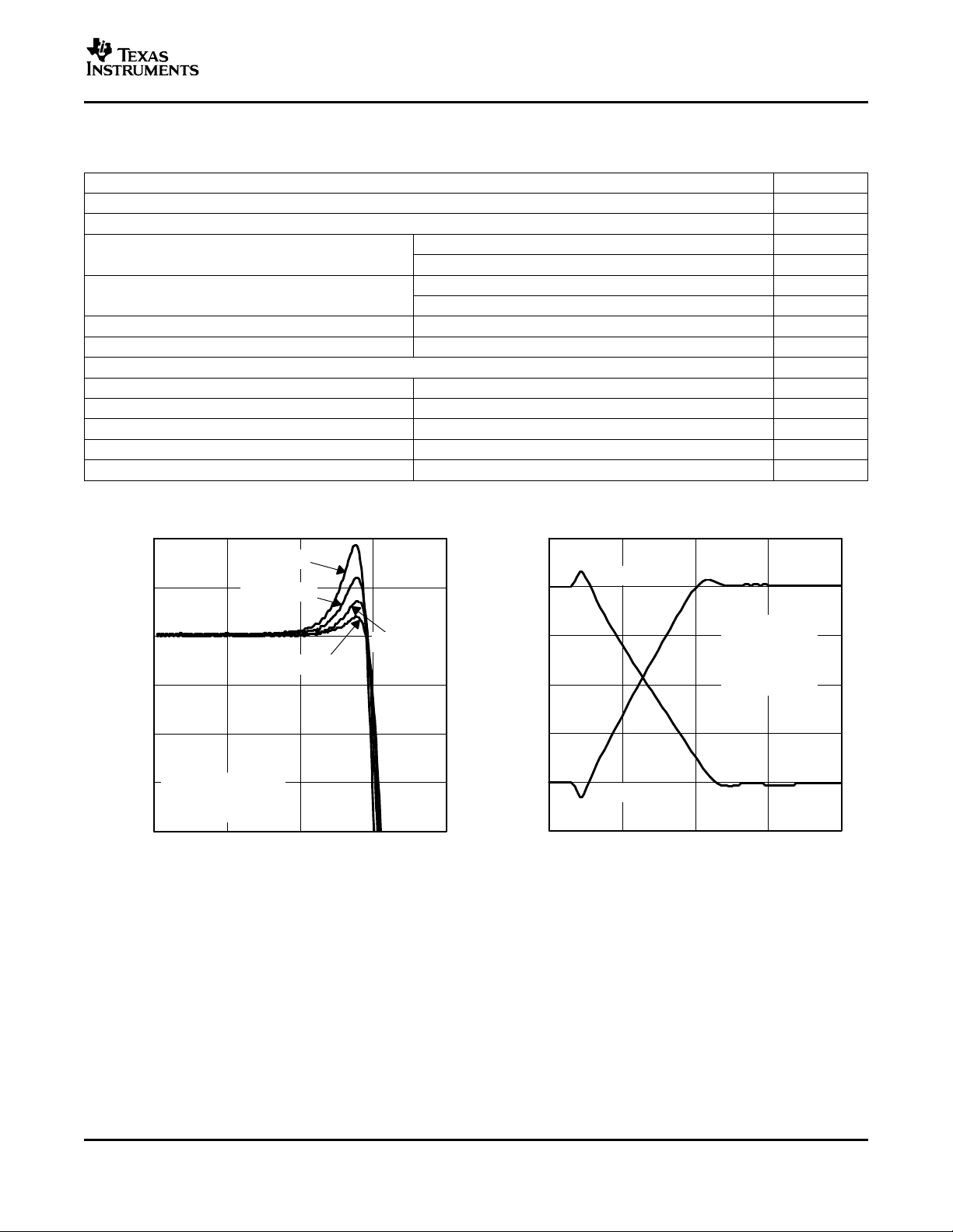
TYPICAL CHARACTERISTICS
Table of Graphs
Small-signal frequency response 1
SR Slew rate 2
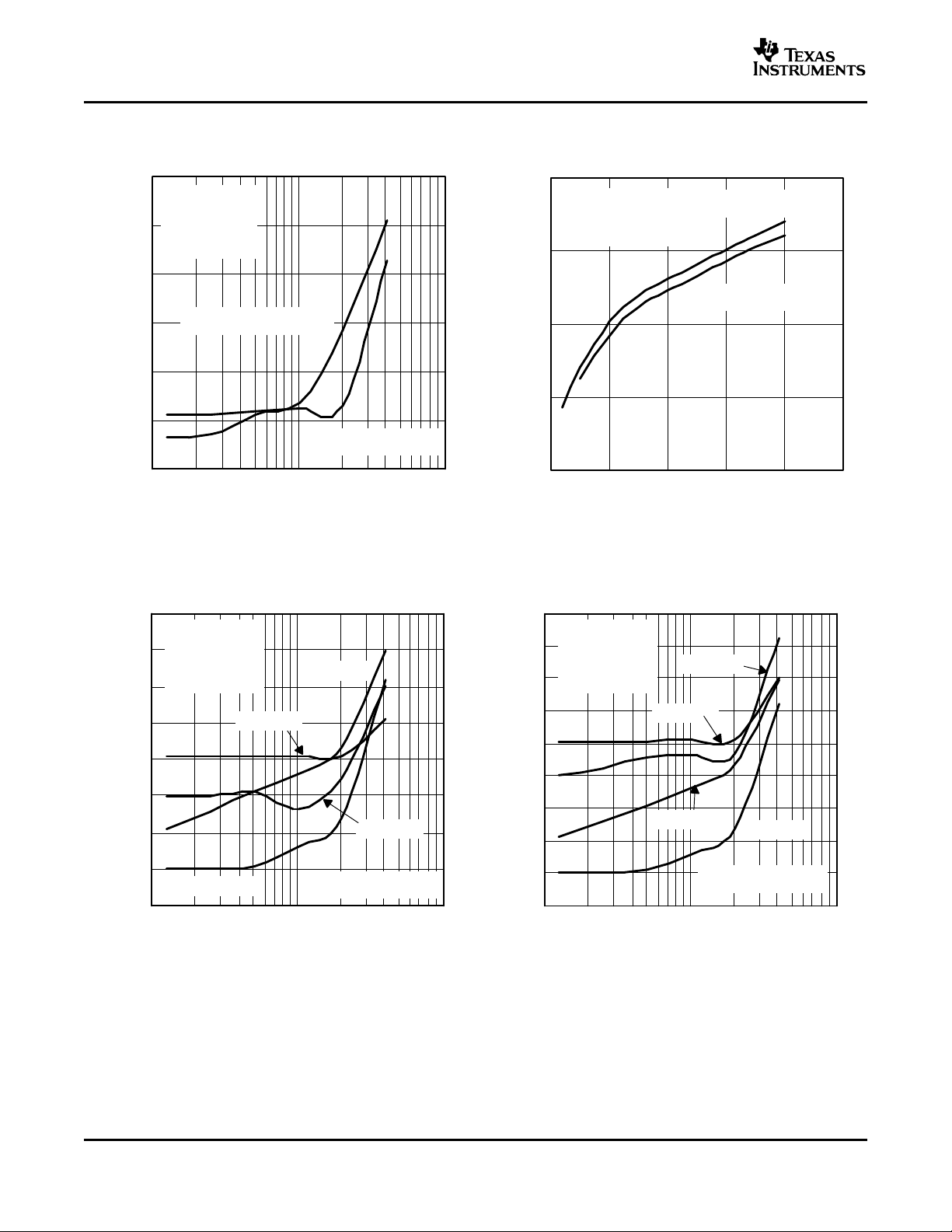
THD Total harmonic distortion
Harmonic distortion
Third intermodulation distortion vs Output voltage 10
V
Output voltage vs Load resistance 11
O
Settling time 12
V
V
Voltage noise vs Frequency 13
n
Output offset voltage vs Common-mode input voltage 14
OO
CMMR Common-mode rejection ratio vs Frequency 15
z
os
z
o
Single-ended output impedance (closed loop) vs Frequency 16
Single-ended (V
) input impedance vs Frequency 17
OCM
vs Frequency 3
vs Output voltage 4
vs Frequency 5, 6, 7
vs Output voltage 8, 9
THS4120
THS4121
FIGURE
SMALL-SIGNAL FREQUENCY RESPONSE SLEW RATE
Figure 1. Figure 2.
5
Page 6
www.ti.com
VO − Output Voltage − V
−90
−80
−70
−60
−50
0 1 2 3 4 5
VDD = 3.3 V ,
f = 1 MHz
Rf = 200 Ω,
RL = 800 Ω
Differential Input /
Differential Output
Single Input /
Differential Output
THD − Total Harmonic Distortion − dB
−80
−70
−60
−50
−40
−30
−20
100 k 1 M 10 M
THD − Total Harmonic Distortion − dB
f − Frequency − Hz
Differential Input/
Differential Output
Single−Ended Input /
Differential Output
VDD = 3.3 V ,
VO = 4 V
PP
Rf = 200 Ω,
RL = 800 Ω
G = 1
−120
−110
−100
−90
−80
−70
−60
−50
−40
100 k 1 M 10 M
Harmonic Distortion − dB
f − Frequency − Hz
5th_HD
4th_HD
3rd_HD
3rd_HD
VDD = 3.3 V ,
VO = 2 VPP,
RL = 800 Ω,
Rf = 270 Ω,
G = 1
3rd_HD2nd_HD
Differential Input /
Differential Output
−120
−110
−100
−90
−80
−70
−60
−50
−40
−30
5th_HD
4th_HD
3rd_HD
2nd_HD
100 k 1 M 10 M
Harmonic Distortion − dB
f − Frequency − Hz
VDD = 3.3 V ,
VO = 4 VPP,
RL = 800 Ω,
Rf = 200 Ω,
G = 1
Differential Input /
Differential Output
THS4120
THS4121
SLOS319D – FEBRUARY 2001 – REVISED OCTOBER 2004
TOTAL HARMONIC DISTORTION TOTAL HARMONIC DISTORTION
TOTAL HARMONIC DISTORTION HARMONIC DISTORTION
vs vs
FREQUENCY OUTPUT VOLTAGE
Figure 3. Figure 4.
THS4121 THS4121
vs vs
FREQUENCY FREQUENCY
6
Figure 5. Figure 6.
Page 7
www.ti.com
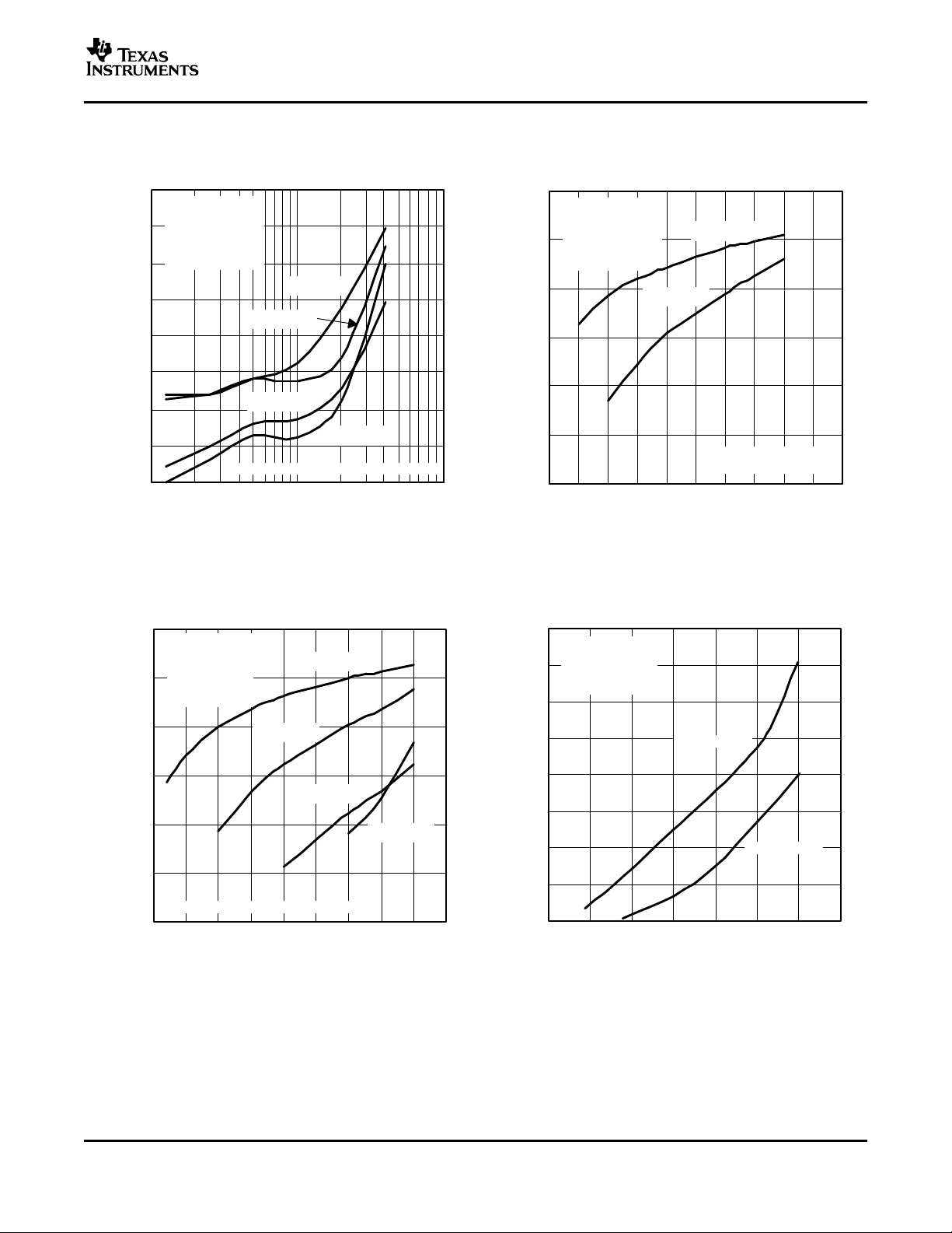
−100
−90
−80
−70
−60
−50
−40
−30
−20
100 k 1 M 10 M
Harmonic Distortion − dB
f − Frequency − Hz
5th_HD
4th_HD
3rd_HD
2nd_HD
VDD = 3.3 V ,
VO = 4 VPP,
RL = 800 Ω,
Rf = 200 Ω,
G = 1
Single Input / Differential Output
Harmonic Distortion − dB
VDD = 3.3 V ,
f = 1 MHz,
RL = 800 Ω,
Rf = 200 Ω,
G = 1
VO − Output Voltage − V
−120
−110
−100
−90
−80
−70
−60
0 0.5 1 1.5 2 2.5 3 3.5 4 4.5 5
3rd_HD
2nd_HD
Differential Input /
Differential Output
−120
−110
−100
−90
−80
−70
−60
0 0.5 1 1.5 2 2.5 3 3.5 4 4.5
Harmonic Distortion − dB
5th_HD
4th_HD
3rd_HD
2nd_HD
VDD = 3.3 V ,
f = 1 MHz,
RL = 800 Ω,
Rf = 200 Ω,
G = 1
Single Input / Differential Output
VO − Output Voltage − V
−90
−80
−70
−60
−50
−40
−30
−20
−10
−25 −20 −15 −10 −5 0 5 10
Third Intermodulation Distortion − dBc
VO − Output Voltage − V
f = 10 MHz
f = 5 MHz
VDD = 3.3 V ,
f = 1 MHz
Rf = 270 Ω,
RL = 800 Ω
THS4120
THS4121
SLOS319D – FEBRUARY 2001 – REVISED OCTOBER 2004
HARMONIC DISTORTION HARMONIC DISTORTION
HARMONIC DISTORTION THIRD INTERMODULALTION DISTORTION
THS4121 THS4121
vs vs
FREQUENCY OUTPUT VOLTAGE
Figure 7. Figure 8.
THS4121
vs vs
OUTPUT VOLTAGE OUTPUT VOLTAGE
Figure 9. Figure 10.
7
Page 8

www.ti.com
0.95
0.96
0.97
0.98
0.99
1
1.01
1.02
1.03
0 100 200 300 400 500
t − Time − ns
− Output Voltage − VV
O
Settling Time,
1% = 40 ns,
0.1% = 60 ns,
0.01% = 292 ns
VDD = 3.3 V ,
VO = 2 VPP,
RF = 330 Ω,
RL = 800 Ω,
G = 1
VDD = 3.3 V
−2
−1.5
−1
−0.5
0
0.5
1
1.5
2
Source
Sink
100
− Output Voltage − V
1k 10k
V
O
RL − Load Resistance − Ω
1 10 100
− Voltage Noise −
f − Frequency − Hz
1 k 10 k
V
n
nV/ Hz
0
20
40
60
80
100
120
140
100 k
−0.4
−0.3
−0.2
−0.1
0
0.1
− Output Offset Voltage − V
− Common-Mode Input Voltage − VV
IC
V
OO
0 0.5 1 1.5 2 2.5 3
THS4120
THS4121
SLOS319D – FEBRUARY 2001 – REVISED OCTOBER 2004
THS4121
OUTPUT VOLTAGE
LOAD RESISTANCE SETTLING TIME
vs
VOLTAGE NOISE OUTPUT OFFSETE VOLTAGE
FREQUENCY COMMON-MODE INPUT VOLTAGE
8
Figure 11. Figure 12.
vs vs
Figure 13. Figure 14.
Page 9

www.ti.com
100 k 1 M
CMRR − Common-Mode Rejection Ratio − dB
f − Frequency − Hz
10 M 100 M
VDD = 3.3 V ,
Rf = 1 kΩ,
RL = 800 Ω,
G = 1
−110
−100
−90
−80
−70
−60
−50
1
10
100
1000
100 k 1 M 10 M 100 M
− Single-Ended Output Impedance −
f − Frequency − Hz
z
os
Ω
VDD = 3.3 V ,
VI = 5 dBm
G = 1
10
100
1 k
10 k
100 k
1 M
100 k 1 M 100 M 1 G
− Single-Ended
f − Frequency − Hz
Z
is
Ω
(V
OCM
)
Input Impedance −
VDD = 3.3 V ,
VI = −0.071 V
(RMS)
10 M
THS4120
THS4121
SLOS319D – FEBRUARY 2001 – REVISED OCTOBER 2004
COMMON-MODE REJECTION RATIO SINGLE-ENDED OUTPUT IMPEDANCE
THS4121 THS4121
vs vs
FREQUENCY FREQUENCY
Figure 15. Figure 16.
SINGLE-ENDED (V
THS4121
) INPUT IMPEDANCE
OCM
vs
FREQUENCY
Figure 17.
9
Page 10

www.ti.com
V
DD
V
SS
2
_
+
x1
Output Buffer
Vcm Error
Amplifier
C R
C
R
x1
Output Buffer
V
OUT+
V
OUT-
V
DD
V
SS
V
IN-
V
IN+
30 kΩ
30 kΩ
V
DD
V
SS
V
OCM
THS4120
THS4121
SLOS319D – FEBRUARY 2001 – REVISED OCTOBER 2004
APPLICATION INFORMATION
RESISTOR MATCHING
Resistor matching is important in fully differential amplifiers. The balance of the output on the reference voltage
depends on matched ratios of the resistors. CMRR, PSRR, and cancellation of the second harmonic distortion
diminish if resistor mismatch occurs. Therefore, it is recommended to use 1% tolerance resistors or better to
keep the performance optimized.
V
sets the dc level of the output signals. If no voltage is applied to the V
OCM
internally defined as:
In the differential mode, the V
mode is the same as the input with the gain of 1. V
on the two outputs cancel each other. Therefore, the output in the differential
OCM
has a high bandwidth capability up to the typical operation
OCM
range of the amplifier. For the prevention of noise going through the device, use a 0.1-µF capacitor on the V
pin as a bypass capacitor. The following graph shows the simplified diagram of the THS412x.
pin, it is set to the midrail voltage
OCM
(1)
OCM
Figure 18. THS412x Simplified Diagram
10
Page 11

www.ti.com
V
IN
-
+
-
+
DV
DD
V
OCM
AV
SS
AV
DD
A
IN2
A
IN1
3.3 V
V
ref
3.3 V
V
DD
0.1 µF
V
DD
V
IN
-
+
-
+
DV
DD
V
OCM
AV
SS
AV
DD
A
IN2
A
IN1
V
ref
3.3 V
V
DD
0.1 µF
V
CC
R
PU
V
CC
R
PU
R
(g)
R
(g)
V
P
R
f
R
f
V
OUT
V
OUT
R
PU
VP– V
DD
VIN– V
P
1
R
(g)
V
OUT
– V
P
1
R
f
SLOS319D – FEBRUARY 2001 – REVISED OCTOBER 2004
DATA CONVERTERS
Data converters are one of the most popular applications for the fully differential amplifiers.
Fully differential amplifiers can operate with a single supply. V
differential output may be fed into a data converter. This method eliminates the use of a transformer in the circuit.
If the ADC has a reference voltage output (V
), then it is recommended to connect it directly to the V
ref
amplifier using a bypass capacitor for stability. For proper operation, the input common-mode voltage to the input
terminal of the amplifier should not exceed the common-mode input voltage range.
Figure 19. Differential Amplifier Using a Single Supply
defaults to the midrail voltage, V
OCM
THS4120
THS4121
/2. The
DD
of the
OCM
Some single-supply applications may require the input voltage to exceed the common-mode input voltage range.
In such cases, the following circuit configuration is suggested to bring the common-mode input voltage within the
specifications of the amplifier.
Figure 20. Circuit With Improved Common-Mode Input Voltage
The following equation is used to calculate R
:
PU
(2)
11
Page 12

www.ti.com
THS412x
Output
Output
20 Ω
20 Ω
R
(g)
R
(g)
R
f
R
f
VIN-
VIN+
+
-
+
V
OCM
V
OCM
VIN-
VIN+
V
SS
THS412x
C3
C3
R4
R
(t)
R2
R4
C1
V
DD
C1
R2
R3
R3
C2
R1
R1
Vs
V
IC
V
DD
DV
DD
AV
DD
THS4120
THS4121
SLOS319D – FEBRUARY 2001 – REVISED OCTOBER 2004
DRIVING A CAPACITIVE LOAD
Driving capacitive loads with high-performance amplifiers is not a problem as long as certain precautions are
taken. The first is to realize that the THS412x has been internally compensated to maximize its bandwidth and
slew rate performance. When the amplifier is compensated in this manner, capacitive loading directly on the
output decreases the device's phase margin leading to high-frequency ringing or oscillations. Therefore, for
capacitive loads of greater than 10 pF, it is recommended that a resistor be placed in series with the output of
the amplifier, as shown in Figure 21 . A minimum value of 20 Ω should work well for most applications. For
example, in 50- Ω transmission systems, setting the series resistor value to 50 Ω both isolates any capacitance
loading and provides the proper line impedance matching at the source end.
Figure 21. Driving a Capacitive Load
ACTIVE ANTIALIAS FILTERING
For signal conditioning in ADC applications, it is important to limit the input frequency to the ADC. Low-pass
filters can prevent the aliasing of the high-frequency noise with the frequency of operation. Figure 22 presents a
method by which the noise may be filtered in the THS412x. Proper ground referencing should be considered.
12
Figure 22. Antialias Filtering
Page 13

www.ti.com
Hd(f)
K
–
f
FSF x fc
2
1
QjfFSF x fc
1
x
Rt
2R4 Rt
1
j2πfR4RtC3
2R4 Rt
Where K
R2
R1
FSF x fc
1
2π 2 x R2R3C1C2
and Q
2 x R2R3C1C2
R3C1 R2C1 KR3C1
FSF Re
2
|Im|
2
and Q
Re
2
|Im|
2
2Re
FSF x fc
1
2πRC 2 x mn
and Q
2 x mn
1 m(1 K
)
THS4120
THS4121
SLOS319D – FEBRUARY 2001 – REVISED OCTOBER 2004
The transfer function for this filter circuit is:
K sets the pass-band gain, fc is the cutoff frequency for the filter, FSF is a frequency scaling factor, and Q is the
quality factor.
Where Re is the real part, and Im is the imaginary part of the complex pole pair. Setting R2 = R, R3 = mR,
C1 = C, and C2 = nC results in:
Start by determining the ratios, m and n, required for the gain and Q of the filter type being designed, then select
C and calculate R for the desired fc.
(3)
(4)
(5)
(6)
13
Page 14

www.ti.com
R
f
R
(g)
R
(g)
R
f
_
+
Differential Amplifier
V
OCM
_
+
_
+
V
DD
V
IN−
V
IN+
V
O+
V
O−
THS412x
Fully Differential Amplifier
GND
Input voltage definition V
ID
V
I
–
V
I–
V
IC
V
I
V
I–
2
Output voltage definition V
OD
V
O
–
V
O–
V
OC
V
O
V
O–
2
Transfer function V
OD
VIDx A
f
Output common−mode voltage V
OC
V
OCM
V
OCM
_
+
_
+
V
DD
V
IN-
V
IN+
V
O+
V
O-
Differential Structure Rejects
Coupled Noise at the Output
Differential Structure Rejects
Coupled Noise at the Input
Differential Structure Rejects
Coupled Noise at the Power Supply
GND
THS4120
THS4121
SLOS319D – FEBRUARY 2001 – REVISED OCTOBER 2004
PRINCIPLES OF OPERATION
THEORY OF OPERATION
The THS412x is a fully differential amplifier. Differential amplifiers are typically differential in/single out, whereas
fully differential amplifiers are differential in/differential out.
Figure 23. Differential Amplifier Versus a Fully Differential Amplifier
To understand the THS412x fully differential amplifiers, the definition for the pinouts of the amplifier are provided.
Figure 24. Definition of the Fully Differential Amplifier
The following schematics depict the differences between the operation of the THS412x, fully differential amplifier,
in two different modes. Fully differential amplifiers can work with differential input or can be implemented as
single in/differential out.
(7)
(8)
(9)
(10)
14
Page 15

www.ti.com
-
R
f
R
(g)
+
+
-
GND
V
DD
R
(g)
R
f
Vs
V
IN-
V
IN+
V
O+
V
O-
V
OCM
Note: For proper operation, maintain
symmetry by setting
Rf1 = Rf2 = Rf and R
(g)
1 = R
(g)
2 = R
(g)
⇒ A = Rf/R
(g)
-
R
f
R
(g)
+
+
-
GND
V
DD
R
(g)
R
f
Vs
V
IN-
V
IN+
V
O+
V
O-
V
OCM
GAIN R
(g)
Ω Rf Ω
1 150 150
RECOMMENDED RESISTOR VALUES
V
O
1
2
V
I
VO –
1
2
V
I
PRINCIPLES OF OPERATION (continued)
THS4120
THS4121
SLOS319D – FEBRUARY 2001 – REVISED OCTOBER 2004
Figure 25. Amplifying Differential Signals
If each output is measured independently, each output is one-half of the input signal when gain is 1. The
following equations express the transfer function for each output:
The second output is equal and opposite in sign:
Fully differential amplifiers may be viewed as two inverting amplifiers. In this case, the equation of an inverting
amplifier holds true for gain calculations. One advantage of fully differential amplifiers is that they offer twice as
much dynamic range compared to single-ended amplifiers. For example, a 1-V
signal of 1 V
. If the output of the amplifier is 2 V
PP
targeted ADC. Using a fully differential amplifier enables the user to break down the output into two 1-V
with opposite signs and feed them into the differential input nodes of the ADC. In practice, the designer has been
able to feed a 2-V peak-to-peak signal into a 1-V differential ADC with the help of a fully differential amplifier. The
final result indicates twice as much dynamic range. Figure 27 illustrates the increase in dynamic range. The gain
factor should be considered in this scenario. The THS412x fully differential amplifier offers an improved CMRR
and PSRR due to its symmetrical input and output. Furthermore, second harmonic distortion is improved. Second
harmonics tend to cancel because of the symmetrical output.
Figure 26. Single In With Differential Out
(11)
(12)
ADC can only support an input
, then it is not practical to feed a 2-V
PP
PP
signal into the
PP
signals
PP
15
Page 16

www.ti.com
V
OCM
_
+
_
+
V
DD
V
IN-
V
IN+
V
O+
V
O-
VOD= 1-0 = 1
VOD = 0-1 = -1
a
b
+1
0
+1
0
V
SS
THS4120
THS4121
SLOS319D – FEBRUARY 2001 – REVISED OCTOBER 2004
PRINCIPLES OF OPERATION (continued)
Figure 27. Fully Differential Amplifier With Two 1-V
Signals
PP
CIRCUIT LAYOUT CONSIDERATIONS
To achieve the levels of high-frequency performance of the THS412x, follow proper printed-circuit board high
frequency design techniques. A general set of guidelines is given below. In addition, a THS412x evaluation board
is available to use as a guide for layout or for evaluating the device performance.
• Ground planes - It is highly recommended that a ground plane be used on the board to provide all components with a
low inductive ground connection. However, in the areas of the amplifier inputs and output, the ground plane can be
removed to minimize the stray capacitance.
• Proper power supply decoupling - Use a 6.8-µF tantalum capacitor in parallel with a 0.1-µF ceramic capacitor on each
supply terminal. It may be possible to share the tantalum among several amplifiers depending on the application, but a
0.1-µF ceramic capacitor should always be used on the supply terminal of every amplifier. In addition, the 0.1-µF
capacitor should be placed as close as possible to the supply terminal. As this distance increases, the inductance in the
connecting trace makes the capacitor less effective. The designer should strive for distances of less than 0.1 inch
between the device power terminals and the ceramic capacitors.
• Sockets - Sockets are not recommended for high-speed operational amplifiers. The additional lead inductance in the
socket pins often lead to stability problems. Surface-mount packages soldered directly to the printed-circuit board is the
best implementation.
• Short trace runs/compact part placements - Optimum high-frequency performance is achieved when stray series
inductance has been minimized. To realize this, the circuit layout should be made as compact as possible, thereby
minimizing the length of all trace runs. Particular attention should be paid to the inverting input of the amplifier. Its length
should be kept as short as possible. This helps to minimize stray capacitance at the input of the amplifier.
• Surface-mount passive components - Using surface-mount passive components is recommended for high-frequency
amplifier circuits for several reasons. First, because of the extremely low lead inductance of surface-mount components,
the problem with stray series inductance is greatly reduced. Second, the small size of surface-mount components
naturally leads to a more compact layout thereby minimizing both stray inductance and capacitance. If leaded
components are used, it is recommended that the lead lengths be kept as short as possible.
POWER-DOWN MODE
The THS4120 features a power-down pin ( PD) which lowers the quiescent current from 11 mA down to 120 µA,
ideal for reducing system power. The power-down pin of the amplifier must be pulled high via a 10-k Ω pullup
resistor between the PD pin and the positive supply (see Figure 28 ) in the absence of an applied voltage, putting
the amplifier in the power-on mode of operation. To turn off (disable) the amplifier in an effort to conserve power,
the power-down pin can be driven towards the negative rail or ground. The threshold voltages for power-on and
power-down are relative to the supply rails and given in the specification tables. Above the Enable Threshold
Voltage, the device is on. Below the Disable Threshold Voltage, the device is off. Behavior in between these
threshold voltages is not specified.
Note that this power-down functionality is just that; the amplifier consumes less power in power-down mode. The
power-down mode is not intended to provide a high-impedance output. The power-down functionality is not
intended to allow use as a 3-state bus driver. When in power-down mode, the impedance looking back into the
output of the amplifier is dominated by the feedback and gain-setting resistors, but the output impedance of the
device itself varies depending on the voltage applied to the outputs.
The time delays associated with turning the device on and off are specified as the time it takes for the amplifier to
reach 50% of the nominal quiescent current. The enable time delay is in the order of microseconds due to the
amplifier moving in and out of the linear mode of operation.
16
Page 17

www.ti.com
_
+
THS4120
10 k
3.3 V
PD
V
OCM
V
IN
10
100
1000
10000
100 k 1 M 10 M 100 M 1 G
− Single-Ended Output Impedance (in Power Down) −
f − Frequency − Hz
z
os
Ω
THS4120
SINGLE-ENDED OUTPUT IMPEDANCE
(IN POWER DOWN)
vs
FREQUENCY
VCC = 3.3 V
THS4120
THS4121
SLOS319D – FEBRUARY 2001 – REVISED OCTOBER 2004
PRINCIPLES OF OPERATION (continued)
Figure 28.
Due to the similarity of the standard inverting amplifier configuration, the output impedance appears to be low
while in the power-down state. This is because the feedback resistor (R
connected to the circuit. Therefore, a current path is allowed between the input of the amplifier and the output of
the amplifier. An example of the closed-loop output impedance is shown in Figure 29 .
) and the gain resistor (R
f
) are still
(g)
Figure 29.
17
Page 18

www.ti.com
DIE
Side View (a)
End View (b) Bottom View (c)
DIE
Thermal
Pad
THS4120
THS4121
SLOS319D – FEBRUARY 2001 – REVISED OCTOBER 2004
GENERAL PowerPAD DESIGN CONSIDERATIONS (APPLICABLE TO DIFFERENTIAL AMPLIFIER FAMILY)
The THS412x is available packaged in a thermally enhanced DGN package, which is a member of the
PowerPAD family of packages. This package is constructed using a downset leadframe on which the die is
mounted [see Figure 30 (a) and Figure 30 (b)]. This arrangement results in the leadframe being exposed as a
thermal pad on the underside of the package [see Figure 30 (c)]. Because this thermal pad has direct thermal
contact with the die, excellent thermal performance can be achieved by providing a good thermal path away from
the thermal pad.
The PowerPAD package allows for both assembly and thermal management in one manufacturing operation.
During the surface-mount solder operation (when the leads are being soldered), the thermal pad can also be
soldered to a copper area underneath the package. Through the use of thermal paths within this copper area,
heat can be conducted away from the package into either a ground plane or other heat-dissipating device.
The PowerPAD package represents a breakthrough in combining the small area and ease of assembly of the
surface mount with the, heretofore, awkward mechanical methods of heatsinking.
More complete details of the PowerPAD installation process and thermal management techniques can be found
in the Texas Instruments Technical Brief, PowerPAD Thermally Enhanced Package (SLMA002 ). This document
can be found at the TI Web site (www.ti.com) by searching on the key word PowerPAD. The document can also
be ordered through your local TI sales office. Refer to literature number SLMA002 when ordering.
A. The thermal pad is electrically isolated from all terminals in the package.
Figure 30. Views of Thermally Enhanced DGN Package
18
Page 19

THERMAL PAD MECHANICAL DATA
www.ti.com
DGN (S-PDSO-G8)
THERMAL INFORMATION
This PowerPAD™ package incorporates an exposed thermal pad that is designed to be attached directly to an
external heatsink. When the thermal pad is soldered directly to the printed circuit board (PCB), the PCB can be
used as a heatsink. In addition, through the use of thermal vias, the thermal pad can be attached directly to a
ground plane or special heatsink structure designed into the PCB. This design optimizes the heat transfer from
the integrated circuit (IC).
For additional information on the PowerPAD package and how to take advantage of its heat dissipating abilities,
refer to Technical Brief, PowerPAD Thermally Enhanced Package, Texas Instruments Literature No. SLMA002
and Application Brief, PowerPAD Made Easy, Tex a s Instruments Literature N o . SLMA004. Both documents are
available at www.ti.com.
The exposed thermal pad dimensions for this package are shown in the following illustration.
8
5
Exposed Thermal Pad
1,73
MAX
NOTE: All linear dimensions are in millimeters
Exposed Thermal Pad Dimensions
1
1,78
MAX
Top View
4
PPTD041
PowerPAD is a trademark of Texas Instruments
Page 20

Page 21

Page 22

Page 23

IMPORTANT NOTICE
Texas Instruments Incorporated and its subsidiaries (TI) reserve the right to make corrections, modifications,
enhancements, improvements, and other changes to its products and services at any time and to discontinue
any product or service without notice. Customers should obtain the latest relevant information before placing
orders and should verify that such information is current and complete. All products are sold subject to TI’s terms
and conditions of sale supplied at the time of order acknowledgment.
TI warrants performance of its hardware products to the specifications applicable at the time of sale in
accordance with TI’s standard warranty. Testing and other quality control techniques are used to the extent TI
deems necessary to support this warranty . Except where mandated by government requirements, testing of all
parameters of each product is not necessarily performed.
TI assumes no liability for applications assistance or customer product design. Customers are responsible for
their products and applications using TI components. To minimize the risks associated with customer products
and applications, customers should provide adequate design and operating safeguards.
TI does not warrant or represent that any license, either express or implied, is granted under any TI patent right,
copyright, mask work right, or other TI intellectual property right relating to any combination, machine, or process
in which TI products or services are used. Information published by TI regarding third-party products or services
does not constitute a license from TI to use such products or services or a warranty or endorsement thereof.
Use of such information may require a license from a third party under the patents or other intellectual property
of the third party, or a license from TI under the patents or other intellectual property of TI.
Reproduction of information in TI data books or data sheets is permissible only if reproduction is without
alteration and is accompanied by all associated warranties, conditions, limitations, and notices. Reproduction
of this information with alteration is an unfair and deceptive business practice. TI is not responsible or liable for
such altered documentation.
Resale of TI products or services with statements different from or beyond the parameters stated by TI for that
product or service voids all express and any implied warranties for the associated TI product or service and
is an unfair and deceptive business practice. TI is not responsible or liable for any such statements.
Following are URLs where you can obtain information on other Texas Instruments products and application
solutions:
Products Applications
Amplifiers amplifier.ti.com Audio www.ti.com/audio
Data Converters dataconverter.ti.com Automotive www.ti.com/automotive
DSP dsp.ti.com Broadband www.ti.com/broadband
Interface interface.ti.com Digital Control www.ti.com/digitalcontrol
Logic logic.ti.com Military www.ti.com/military
Power Mgmt power.ti.com Optical Networking www.ti.com/opticalnetwork
Microcontrollers microcontroller.ti.com Security www.ti.com/security
Telephony www.ti.com/telephony
Video & Imaging www.ti.com/video
Wireless www.ti.com/wireless
Mailing Address: Texas Instruments
Post Office Box 655303 Dallas, Texas 75265
Copyright 2004, Texas Instruments Incorporated
 Loading...