

Page 1
查询THS4061供应商
THS4061, THS4062
180-MHz HIGH-SPEED AMPLIFIERS
SLOS234D – DECEMBER 1998 – REVISED FEBRUARY 2000
D
High Speed
– 180 MHz Bandwidth (G = 1, –3 dB)
– 400 V/µs Slew Rate
– 40-ns Settling Time (0.1%)
D
High Output Drive, IO = 115 mA (typ)
D
Excellent Video Performance
– 75 MHz 0.1 dB Bandwidth (G = 1)
– 0.02% Differential Gain
– 0.02° Differential Phase
D
Very Low Distortion
– THD = –72 dBc at f = 1 MHz
D
Wide Range of Power Supplies
– VCC = ±5 V to ±15 V
D
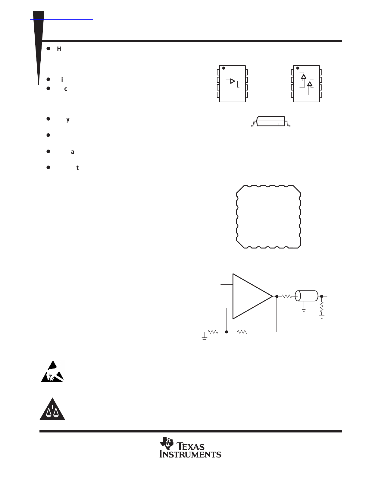
Available in Standard SOIC, MSOP
PowerPAD, JG, or FK Package
D
Evaluation Module Available
description
The THS4061 and THS4062 are generalpurpose, single/dual, high-speed voltage feedback amplifiers ideal for a wide range of
applications including video, communication, and
imaging. The devices offer very good ac
performance with 180-MHz bandwidth, 400-V/µs
slew rate, and 40-ns settling time (0.1% ). The
THS4061/2 are stable at all gains for both
inverting and noninverting configurations. These
amplifiers have a high output drive capability of
1 15 mA and draw only 7.8 mA supply current per
channel. Excellent professional video results can
be obtained with the low differential gain/phase
errors of 0.02%/0.02° and wide 0.1 db flatness to
75 MHz. For applications requiring low distortion,
the THS4061/2 is ideally suited with total
harmonic distortion of –72 dBc at f = 1 MHz.
IN–
IN+
CC–
THS4061
(TOP VIEW)
1
2
3
4
NULL
8
V
7
CC+
OUT
6
5
NC
Cross-Section View Showing
PowerPAD Option (DGN)
FK PACKAGE
(TOP VIEW)
JG, D AND DGN PACKAGE
NULL
V
NC – No internal connection
NC
NC
4
IN–
5
NC
6
IN+
7
NC
8
NC
V
+
I
THS4061
_
D AND DGN PACKAGE
1OUT
1IN–
1IN+
–V
CC
THS4061
NULLNCNULL
1920132
1312119 10
NCNCNC
CC–
V
75 Ω
THS4062
(TOP VIEW)
1
2
3
4
NC
NC
18
V
17
CC+
NC
16
OUT
15
NC
14
75 Ω
75 Ω
8
7
6
5
V
CC+
2OUT
2IN–
2IN+
V
O
CAUTION: The THS4061 and THS4062 provide ESD protection circuitry. However , permanent damage can still occur if this
device is subjected to high-energy electrostatic discharges. Proper ESD precautions are recommended to avoid any
performance degradation or loss of functionality
Please be aware that an important notice concerning availability, standard warranty, and use in critical applications of
Texas Instruments semiconductor products and disclaimers thereto appears at the end of this data sheet.
PowerPAD is a trademark of Texas Insruments Incorporated.
PRODUCTION DATA information is current as of publication date.
Products conform to specifications per the terms of Texas Instruments
standard warranty. Production processing does not necessarily include
testing of all parameters.
POST OFFICE BOX 655303 • DALLAS, TEXAS 75265
2 kΩ
2 kΩ
LINE DRIVER (G = 2)
Copyright 2000, Texas Instruments Incorporated
On products compliant to MIL-PRF-38535, all parameters are tested
unless otherwise noted. On all other products, production
processing does not necessarily include testing of all parameters.
1
Page 2
THS4061, THS4062
180-MHz HIGH-SPEED AMPLIFIERS
SLOS234D – DECEMBER 1998 – REVISED FEBRUARY 2000
RELATED DEVICES
DEVICE DESCRIPTION
THS4011/2
THS4031/2
THS4061/2
T
A
0°C to
70°C
–40°C to
85°C
–55°C to
125°C
†
The D and DGN packages are available taped and reeled. Add an R suffix to the device type (i.e., THS4061CDGNR).
NUMBER OF
CHANNELS
1 THS4061CD THS4061CDGN — — TIABS THS4061EVM
2 THS4062CD THS4062CDGN — — TIABM THS4062EVM
1 THS4061ID THS4061IDGN — — TIABT —
2 THS4062ID THS4062IDGN — — TIABN —
1 — — THS4061MJG THS4061MFK — —
PLASTIC
SMALL
OUTLINE
(D)
†
290-MHz Low Distortion High-Speed Amplifiers
100-MHz Low Noise High Speed-Amplifiers
180-MHz High-Speed Amplifiers
AVAILABLE OPTIONS
PACKAGED DEVICES
PLASTIC
MSOP
(DGN)
†
CERAMIC
DIP
(JG)
CHIP
CARRIER
(FK)
SYMBOL
MSOP
EVALUATION
MODULES
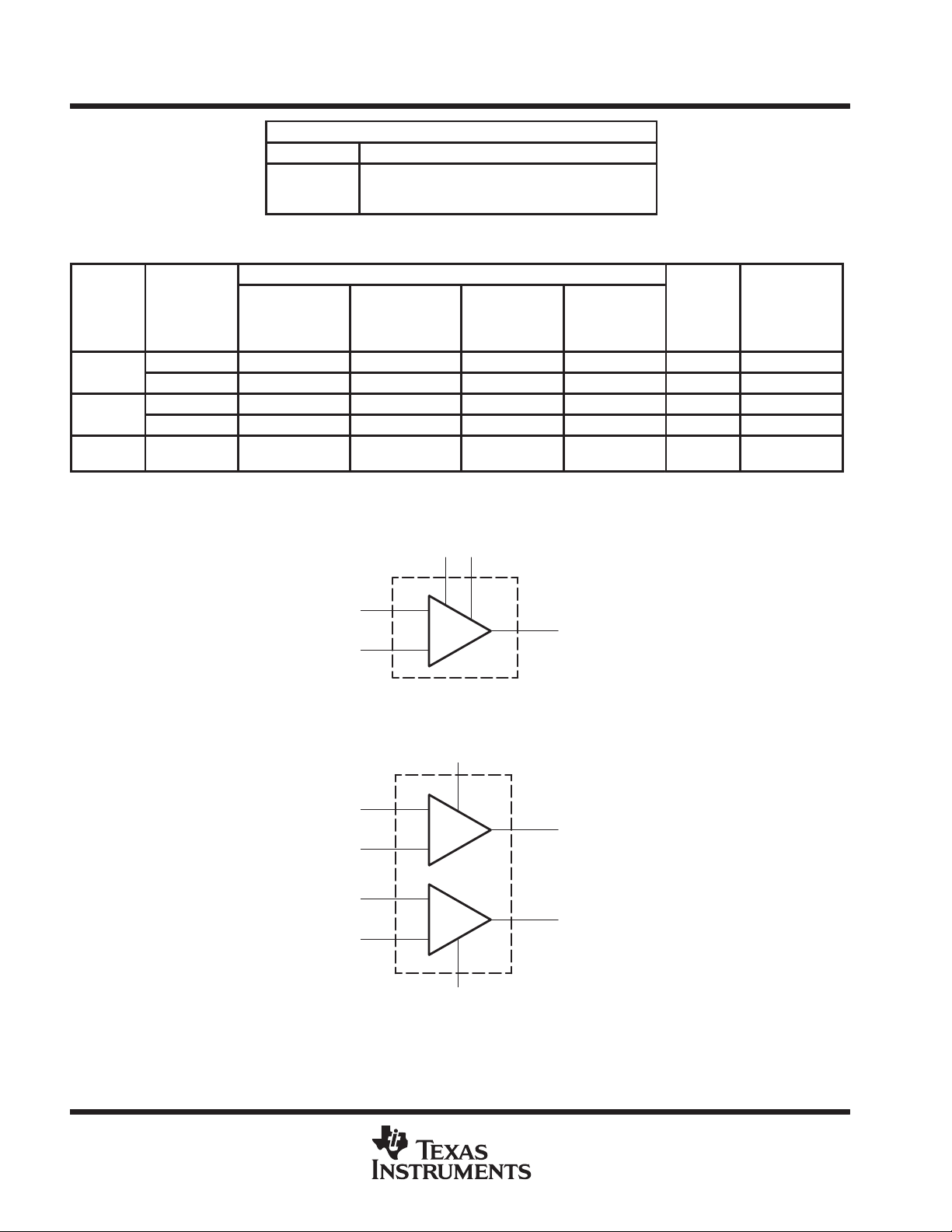
functional block diagram
Null
1
IN–
IN+
2
3
+
8
–
6
OUT
Figure 1. THS4061 – Single Channel
V
CC
1IN–
1IN+
2IN–
2IN+
2
3
6
5
8
–
+
–
+
4
1
1OUT
7
2OUT
–V
CC
Figure 2. THS4062 – Dual Channel
2
POST OFFICE BOX 655303 • DALLAS, TEXAS 75265
Page 3
PACKAGE
A
A
A
A
Suppl
oltage, V
and V
V
THS4061, THS4062
180-MHz HIGH-SPEED AMPLIFIERS
SLOS234D – DECEMBER 1998 – REVISED FEBRUARY 2000
absolute maximum ratings over operating free-air temperature (unless otherwise noted)
†
Supply voltage, VCC+ to VCC– 33 V. . . . . . . . . . . . . . . . . . . . . . . . . . . . . . . . . . . . . . . . . . . . . . . . . . . . . . . . . . . . . .
Input voltage, VI ±V
. . . . . . . . . . . . . . . . . . . . . . . . . . . . . . . . . . . . . . . . . . . . . . . . . . . . . . . . . . . . . . . . . . . . . . . . . .
Output current, IO 150 mA. . . . . . . . . . . . . . . . . . . . . . . . . . . . . . . . . . . . . . . . . . . . . . . . . . . . . . . . . . . . . . . . . . . . . . .
Differential input voltage, V
±4 V. . . . . . . . . . . . . . . . . . . . . . . . . . . . . . . . . . . . . . . . . . . . . . . . . . . . . . . . . . . . . . . .
IO
Continuous total power dissipation See Dissipation Rating Table. . . . . . . . . . . . . . . . . . . . . . . . . . . . . . . . . . . . .
Maximum junction temperature, TJ 150°C. . . . . . . . . . . . . . . . . . . . . . . . . . . . . . . . . . . . . . . . . . . . . . . . . . . . . . . . .
Operating free-air temperature, TA: C-suffix 0°C to 70°C. . . . . . . . . . . . . . . . . . . . . . . . . . . . . . . . . . . . . . . . . . .
I-suffix –40°C to 85°C. . . . . . . . . . . . . . . . . . . . . . . . . . . . . . . . . . . . . . . . . .
M-suffix –55°C to 125°C. . . . . . . . . . . . . . . . . . . . . . . . . . . . . . . . . . . . . . . .
Storage temperature, T
–65°C to 150°C. . . . . . . . . . . . . . . . . . . . . . . . . . . . . . . . . . . . . . . . . . . . . . . . . . . . . . . . .
stg
Lead temperature 1,6 mm (1/16 inch) from case for 10 seconds, D and DGN package 300°C. . . . . . . . . . . .
Lead temperature 1,6 mm (1/16 inch) from case for 60 seconds, JG package 300°C. . . . . . . . . . . . . . . . . . . .
Case temperature for 60 seconds, FK package 260°C. . . . . . . . . . . . . . . . . . . . . . . . . . . . . . . . . . . . . . . . . . . . . .
†
Stresses beyond those listed under “absolute maximum ratings” may cause permanent damage to the device. These are stress ratings only and
functional operation of the device at these or any other conditions beyond those indicated under “recommended operating conditions” is not
implied. Exposure to absolute-maximum-rated conditions for extended periods may affect device reliability.
DISSIPATION RATING TABLE
T
≤ 25°C DERATING FACTOR T
POWER RATING ABOVE TA = 25°C
D 740 mW 6 mW/°C 475 mW 385 mW —
‡
DGN
JG 1057 mW 8.4 mW/°C 627 mW 546 mW 210 mW
FK 1375 mW 11 mW/°C 880 mW 715 mW 275 mW
‡
The DGN package incorporates a PowerPAD on the underside of the device. This acts as a heatsink and must be connected to a thermal dissipation
plane for proper power dissipation. Failure to do so can result in exceeding the maximum specified junction temperature, which could permanently
damage the device.
2.14 W 17.1 mW/°C 1.37 W 1.11 W —
= 70°C T
POWER RATING
= 85°C T
POWER RATING
= 125°C
POWER RATING
CC
recommended operating conditions
pp
y v
Operating free-air temperature, T
CC
+
CC
–
A
MIN NOM MAX UNIT
Dual supply ±4.5 ±16
Single supply 9 32
C-suffix 0 70
I-suffix –40 85
M-suffix –55 125
°C
POST OFFICE BOX 655303 • DALLAS, TEXAS 75265
3
Page 4
THS4061, THS4062
†
bandwidth (–3 dB)
Gain
1
MH
Bandwidth for 0.1 dB flatness
Gain
1
MH
SR
Slew rate
Gain
1
V/µs
Settling time to 0.1%
Gain
1
ns
t
Settling time to 0.01%
Gain
1
ns
†
Differential gain error
Gain
NTSC
IRE modulation
Differential phase error
Gain
NTSC
IRE modulation
†
V
±15 V,V
±10 V
R
1 kΩ
V/mV
Open loop gain
V
V
R
kΩ
V/mV
V
T
full range
180-MHz HIGH-SPEED AMPLIFIERS
SLOS234D – DECEMBER 1998 – REVISED FEBRUARY 2000
electrical characteristics at TA = 25°C, VCC = ±15 V, RL = 150 Ω (unless otherwise noted)
dynamic performance
THS4061C/I,
PARAMETER
Dynamic performance small-signal
BW
s
†
Full range = 0°C to 70°C for C suffix and –40°C to 85°C for I suffix
–
VCC = ±5 V Gain = 1 180 MHz
VCC = ±15 V
VCC = ±5 V
VCC = ±15 V
VCC = ±5 V
VCC = ±15 V
VCC = ±5 V
VCC = ±15 V, 5-V step (0 V to 5 V)
VCC = ±5 V, VO = –2.5 V to 2.5 V,
VCC = ±15 V, 5-V step (0 V to 5 V)
VCC = ±5 V, VO = –2.5 V to 2.5 V,
TEST CONDITIONS
= –
=
= –
= –
= –
THS4062C/I
MIN TYP MAX
50
50
75
20
400
350
40
40
140
150
UNIT
z
z
noise/distortion performance
THS4061C/I,
PARAMETER
THD Total harmonic distortion f = 1 MHz –72 dBc
V
I
n
†
Full range = 0°C to 70°C for C suffix and –40°C to 85°C for I suffix
Input voltage noise f = 10 kHz, VCC = ±5 V or ±15 V 14.5 nV/√Hz
n
Input current noise f = 10 kHz, VCC = ±5 V or ±15 V 1.6 pA/√Hz
= 2,
p
Channel-to-channel crosstalk
(THS4062 only)
= 2,
VCC = ±5 V or ±15 V, f = 1 MHz 65 dB
TEST CONDITIONS
, 40
, 40
VCC = ±15 V
VCC = ±5 V
VCC = ±15 V 0.02°
VCC = ±5 V 0.06°
THS4062C/I
MIN TYP MAX
0.02
%
0.02
%
dc performance
THS4061C/I,
PARAMETER
=
CC
p
p
= ±5 V,
CC
Input offset voltage VCC = ±5 V or ±15 V
OS
Offset drift VCC = ±5 V or ±15 V
I
IB
I
OS
†
Full range = 0°C to 70°C for C suffix and –40°C to 85°C for I suffix
Input bias current VCC = ±5 V or ±15 V TA = full range 3 6 µA
Input offset current VCC = ±5 V or ±15 V TA = full range 75 250 nA
Offset current drift TA = full range 0.3 nA/°C
O
O
TEST CONDITIONS
=
= ±2.5 V,
,
L
L
=
= 1
TA = 25°C 5 15
TA = full range 4
TA = 25°C 2.5 8
TA = full range 2
=
A
THS4062C/I
MIN TYP MAX
2.5 8 mV
15 µV/°C
UNIT
UNIT
4
POST OFFICE BOX 655303 • DALLAS, TEXAS 75265
Page 5
†
V
Common-mode input voltage range
V
CMRR
Common mode rejection ratio
T
full range
dB
†
V
VOOutput voltage swing
R
kΩ
V
IOOutput current
R
Ω
mA
†
VCCSuppl
oltage operating range
V
ICCQuiescent current (per amplifier)
T
full range
mA
PSRR
Power supply rejection ratio
V
±15 V
dB
THS4061, THS4062
180-MHz HIGH-SPEED AMPLIFIERS
SLOS234D – DECEMBER 1998 – REVISED FEBRUARY 2000
electrical characteristics at TA = 25°C, VCC = ±15 V , RL = 150 Ω (unless otherwise noted) (continued)
input characteristics
THS4061C/I,
PARAMETER
ICR
R
C
†
Full range = 0°C to 70°C for C suffix and –40°C to 85°C for I suffix
Input resistance 1 MΩ
I
Input capacitance 2 pF
i
p
VCC = ±15 V ±13.8 ±14.1
VCC = ±5 V ±3.8 ±4.3
VCC = ±15 V, V
VCC = ±5 V, V
output characteristics
PARAMETER
VCC = ±15 V RL = 250 Ω ±11.5 ±12.5
p
p
I
SC
R
†
Full range = 0°C to 70°C for C suffix and –40°C to 85°C for I suffix
Short-circuit current VCC = ±15 V 150 mA
Output resistance Open loop 12 Ω
O
VCC = ±5 V RL = 150 Ω ±3.2 ±3.5
VCC = ±15 V
VCC = ±5 V
VCC = ±15 V
VCC = ±5 V
TEST CONDITIONS
= ±12 V
ICR
= ±2.5 V
ICR
TEST CONDITIONS
=
A
L
L
= 1
= 20
THS4062C/I
MIN TYP MAX
70 110
70 95
THS4061C/I,
THS4062C/I
MIN TYP MAX
±13 ±13.5
±3.5 ±3.7
80 115
50 75
UNIT
UNIT
power supply
PARAMETER
pp
y v
†
Full range = 0°C to 70°C for C suffix and –40°C to 85°C for I suffix
pp
p
p
p
Dual supply ±4.5 ±16.5
Single supply 9 33
VCC = ±15 V
VCC = ±5 V
= ±5 V or
CC
TEST CONDITIONS
THS4061C/I,
THS4062C/I
MIN TYP MAX
=
A
TA = 25°C 70 78
TA = full range 68
7.8 10.5
7.3 10
UNIT
POST OFFICE BOX 655303 • DALLAS, TEXAS 75265
5
Page 6
THS4061, THS4062
PARAMETER
TEST CONDITIONS
†
UNIT
Gain
1
MH
yg
Gain
1
MH
Bandwidth for 0.1 dB flatness
Gain
1
MH
Settling time to 0.1%
Gain
1
ns
t
Settling time to 0.01%
Gain
1
ns
PARAMETER
TEST CONDITIONS
†
UNIT
Differential gain error
Gain
NTSC
IRE Modulation
%
Differential phase error
Gain
NTSC
IRE Modulation
PARAMETER
TEST CONDITIONS
†
UNIT
Open loop gain
T
range
V/mV
Input offset voltage
V
±5 V or ±15 VR
1 kΩ
180-MHz HIGH-SPEED AMPLIFIERS
SLOS234D – DECEMBER 1998 – REVISED FEBRUARY 2000
electrical characteristics at TA = 25°C, VCC = ±15 V, RL = 150 Ω (unless otherwise noted)
dynamic performance
THS4061M
MIN TYP MAX
Unity-gain bandwidth Closed loop, RL = 1 kΩ VCC = ±15 V *140 180 MHz
VCC = ±15 V
Dynamic performance small-signal
BW
SR Slew rate VCC = ±15 V RL = 1 kΩ *400 500 V/µs
s
†
Full range = –55°C to 125°C for M suffix
*This parameter is not tested.
bandwidth (–3 dB)
VCC = ±5 V
VCC = ±15 V
VCC = ±5 V
VCC = ±15 V
VCC = ±5 V
VCC = ±15 V, 5-V step (0 V to 5 V)
VCC = ±5 V, VO = –2.5 V to 2.5 V,
VCC = ±15 V, 5-V step (0 V to 5 V)
VCC = ±5 V, VO = –2.5 V to 2.5 V,
=
= –
=
= –
= –
180
180
50
50
75
20
40
40
140
150
z
z
z
noise/distortion performance
THS4061M
MIN TYP MAX
THD Total harmonic distortion f = 1 MHz –72 dBc
V
I
n
†
Full range = –55°C to 125°C for M suffix
Input voltage noise f = 10 kHz, VCC = ±5 V or ±15 V 14.5 nV/√Hz
n
Input current noise f = 10 kHz, VCC = ±5 V or ±15 V 1.6 pA/√Hz
= 2,
p
= 2,
, 40
, 40
VCC = ±15 V 0.02
VCC = ±5 V 0.02
VCC = ±15 V 0.02°
VCC = ±5 V 0.06°
dc performance
THS4061M
MIN TYP MAX
p
p
V
IO
I
IB
I
IO
†
Full range = –55°C to 125°C for M suffix
p
Offset drift VCC = ±5 V or ±15 V RL = 1 kΩ TA = full range 15 µV/°C
Input bias current VCC = ±5 V or ±15 V RL = 1 kΩ TA = full range 3 6 µA
Input offset current VCC = ±5 V or ±15 V RL = 1 kΩ TA = full range 75 250 nA
Offset current drift VCC = ±5 V or ±15 V RL = 1 kΩ TA = full range 0.3 nA/°C
VCC = ±15 V, VO = ±10 V, RL = 1 kΩ
VCC = ±5 V, VO = ±2.5 V, RL = 1 kΩ
CC
=
=
L
= full
A
TA = 25°C 2.5 8 mV
TA = full range 9 mV
5 9
2.5 6
6
POST OFFICE BOX 655303 • DALLAS, TEXAS 75265
Page 7
PARAMETER
TEST CONDITIONS
†
UNIT
V
Common-mode input voltage range
V
CMRR
Common mode rejection ratio
dB
PARAMETER
TEST CONDITIONS
†
UNIT
V
VOOutput voltage swing
R
kΩ
V
IOOutput current
R
Ω
mA
PARAMETER
TEST CONDITIONS
†
UNIT
VCCSuppl
oltage operating range
V
T
25°C
ICCQuiescent current
mA
T
range
PSRR
Power supply rejection ratio
V
±15 V
dB
THS4061, THS4062
180-MHz HIGH-SPEED AMPLIFIERS
SLOS234D – DECEMBER 1998 – REVISED FEBRUARY 2000
electrical characteristics at TA = full range, VCC = ±15 V, RL = 1 kΩ (unless otherwise noted)
(continued)
input characteristics
THS4061M
MIN TYP MAX
ICR
R
C
†
Full range = –55°C to 125°C for M suffix
Input resistance 1 MΩ
I
Input capacitance 2 pF
i
p
output characteristics
p
p
I
SC
R
†
Full range = –55°C to 125°C for M suffix
Short-circuit current VCC = ±15 V TA = 25°C 150 mA
Output resistance Open loop 12 Ω
O
VCC = ±15 V ±13.8 ±14.1
VCC = ±5 V ±3.8 ±4.3
VCC = ±15 V, V
VCC = ±5 V, V
VCC = ±15 V RL = 250 Ω ±12 ±13.1
VCC = ±5 V RL = 150 Ω ±3.2 ±3.5
VCC = ±15 V
VCC = ±5 V
VCC = ±15 V
VCC = ±5 V
= ±12 V 70 86
ICR
= ±2.5 V 80 90
ICR
MIN TYP MAX
= 1
L
= 20
L
±13 ±13.5
±3.5 ±3.7
70 115
50 75
THS4061M
power supply
pp
y v
†
Full range = –55°C to 125°C for M suffix
p
pp
THS4061M
MIN TYP MAX
Dual supply ±4.5 ±16.5
Single supply 9 33
VCC = ±15 V
VCC = ±5 V
VCC = ±15 V
VCC = ±5 V
= ±5 V or
CC
°
=
A
= full
A
TA = 25°C 76 80
TA = full range 74 78
7.8 9
7.3 8.5
11
10.5
POST OFFICE BOX 655303 • DALLAS, TEXAS 75265
7
Page 8

THS4061, THS4062
PSRR
Power-supply rejection ratio
180-MHz HIGH-SPEED AMPLIFIERS
SLOS234D – DECEMBER 1998 – REVISED FEBRUARY 2000
TYPICAL CHARACTERISTICS
I
IB
V
IO
CMRR Common-mode rejection ratio vs Frequency 14
V
O(PP)
I
CC
E
nv
THD Total harmonic distortion vs Frequency 20, 21
Input bias current vs Free-air temperature 3
Input offset voltage vs Free-air temperature 4
Open-loop gain vs Frequency 5
Phase vs Frequency 5
Differential gain vs Number of loads 6, 8
Differential phase vs Number of loads 7, 9
Closed-loop gain vs Frequency 10, 11
Output Amplitude vs Frequency 12, 13
pp
Output voltage swing vs Supply voltage 17
Supply current vs Free-air temperature 18
Noise spectral density vs Frequency 19
FIGURE
vs Frequency 15
vs Free-air temperature 16
8
POST OFFICE BOX 655303 • DALLAS, TEXAS 75265
Page 9
THS4061, THS4062
180-MHz HIGH-SPEED AMPLIFIERS
SLOS234D – DECEMBER 1998 – REVISED FEBRUARY 2000
TYPICAL CHARACTERISTICS
INPUT BIAS CURRENT
vs
FREE-AIR TEMPERATURE
4
VCC = ±15 V, ±5 V
3.5
3
– Input Bias Current – Aµ
2.5
IB
I
2
–40 –20 0 20 80
TA – Free-Air Temperature – °C
Figure 3
90
80
70
0
–0.5
–1
–1.5
–2
–2.5
– Input Offset Voltage – mV
IO
V
–3
6040
100
–3.5
–40 –20 0 804020
OPEN-LOOP GAIN AND PHASE
vs
FREQUENCY
VCC = ±15 V
VCC = ±5 V
INPUT OFFSET VOLTAGE
vs
FREE-AIR TEMPERATURE
VCC = ±5 V
VCC = ±15 V
60
TA – Free-Air Temperature – °C
Figure 4
0°
100
60
50
40
30
Open-Loop Gain – dB
20
10
0
10k 1M
1k
POST OFFICE BOX 655303 • DALLAS, TEXAS 75265
Phase
100k 10M 100M
f – Frequency – Hz
Figure 5
1G
–45°
–90°
–135°
–180°
Phase
9
Page 10

THS4061, THS4062
180-MHz HIGH-SPEED AMPLIFIERS
SLOS234D – DECEMBER 1998 – REVISED FEBRUARY 2000
TYPICAL CHARACTERISTICS
0.14%
Gain = 2
0.12%
0.08%
0.06%
Differential Gain
0.04%
0.02%
0.2%
0.18%
0.16%
0.14%
0.12%
RF = 680 Ω
40 IRE – NTSC
Worst Case ±100 IRE Ramp
0.1%
0%
1
Gain = 2
RF = 680 Ω
40 IRE – PAL
Worst Case ±100 IRE Ramp
DIFFERENTIAL GAIN
vs
NUMBER OF LOADS
VCC = ±15
Gain
VCC = ±5
Gain
23
Number of 150 Ω Loads
Figure 6
DIFFERENTIAL GAIN
vs
NUMBER OF LOADS
VCC = ±15
Gain
0.7°
0.6
0.5°
0.4°
0.3°
Differential Phase
0.2°
0.1°
4
DIFFERENTIAL PHASE
NUMBER OF LOADS
Gain = 2
RF = 680 Ω
40 IRE – NTSC
Worst Case ±100 IRE Ramp
VCC = ±15
Phase
0°
1
Number of 150 Ω Loads
DIFFERENTIAL PHASE
NUMBER OF LOADS
1°
Gain = 2
0.9°
RF = 680 Ω
40 IRE – PAL
0.8°
Worst Case ±100 IRE Ramp
0.7°
0.6°
vs
VCC = ±5
Phase
23
Figure 7
vs
4
0.1%
0.08%
Differential Gain
0.06%
0.04%
0.02%
0%
10
VCC = ±5
Gain
1
23
Number of 150 Ω Loads
4
Figure 8
POST OFFICE BOX 655303 • DALLAS, TEXAS 75265
0.5°
0.4°
Differential Phase
0.3°
0.2°
0.1°
0°
1
VCC = ±5
Phase
VCC = ±15
Phase
23
Number of 150 Ω Loads
Figure 9
4
Page 11

THS4061, THS4062
180-MHz HIGH-SPEED AMPLIFIERS
SLOS234D – DECEMBER 1998 – REVISED FEBRUARY 2000
TYPICAL CHARACTERISTICS
CLOSED-LOOP GAIN
2
0
–2
–4
–6
–8
Closed-Loop Gain – dB
–10
Gain = 1
–12
RF = 270 Ω
RL = 150 Ω
–14
100k
1M 100M
OUTPUT AMPLITUDE
4
vs
FREQUENCY
VCC = ±15 V
VCC = ±5 V
10M 1G
f – Frequency – Hz
Figure 10
vs
FREQUENCY
CLOSED-LOOP GAIN
5
0
–5
–10
Closed-Loop Gain – dB
VCC = ±15 V, ±5 V
–15
Gain = –1
RF = 510 Ω
RL = 150 Ω
–20
100k
1M 100M
OUTPUT AMPLITUDE
2
vs
FREQUENCY
10M 1G
f – Frequency – Hz
Figure 11
vs
FREQUENCY
2
0
–2
–4
Output Amplitude – dB
–6
Gain = 1
RL = 150 Ω
–8
100k 1M 10M 100M 1G
RF = 1 kΩ
RF = 270 Ω
RF = 200 Ω
f – Frequency – Hz
Figure 12
RF = 510 Ω
0
–2
–4
–6
Output Amplitude – dB
–8
Gain = –1
RL = 150 Ω
–10
100k 1M 10M 100M 1G
RF = 3 kΩ
f – Frequency – Hz
Figure 13
POST OFFICE BOX 655303 • DALLAS, TEXAS 75265
11
Page 12

THS4061, THS4062
180-MHz HIGH-SPEED AMPLIFIERS
SLOS234D – DECEMBER 1998 – REVISED FEBRUARY 2000
TYPICAL CHARACTERISTICS
COMMON-MODE REJECTION RATIO
vs
FREQUENCY
120
VCC = ±15 V, ±5 V
100
80
60
40
20
CMRR – Common-Mode Rejection Ratio – dB
0
10k 10M 100M
1M100k
f – Frequency – Hz
Figure 14
POWER SUPPLY REJECTION RATIO
vs
FREE-AIR TEMPERATURE
90
POWER SUPPLY REJECTION RATIO
vs
FREQUENCY
–80
–70
–60
–50
–40
–30
–20
–10
PSRR – Power Supply Rejection Ratio – dB
VCC = ±15 V, ±5 V
0
1k 10k 10M 100M1M100k
f – Frequency – Hz
Figure 15
OUTPUT VOLTAGE SWING
vs
SUPPLY VOLTAGE
30
88
86
84
82
80
78
76
74
PSRR – Power Supply Rejection Ratio – dB
72
–40 –20 0 804020
VCC = 15 V
TA – Free-Air Temperature – °C
VCC = –15 V
Figure 16
60 100
25
RL = 1 kΩ
20
RL = 150 Ω
15
10
– Output Voltage Swing – V
O(PP)
5
V
0
±4 ±6 ±8 ±10 ±16
VCC – Supply Voltage – V
Figure 17
±14±12
12
POST OFFICE BOX 655303 • DALLAS, TEXAS 75265
Page 13

THS4061, THS4062
180-MHz HIGH-SPEED AMPLIFIERS
SLOS234D – DECEMBER 1998 – REVISED FEBRUARY 2000
TYPICAL CHARACTERISTICS
SUPPLY CURRENT
vs
FREE-AIR TEMPERATURE
10
9
8
7
– Supply Current – mA
6
CC
I
5
4
–40 –20 0 20 80
VCC = ±15 V
VCC = ±5 V
TA – Free-Air Temperature – °C
Figure 18
TOTAL HARMONIC DISTORTION
vs
FREQUENCY
–40
Gain = 2
VCC = ±15 V
–50
RL = 150 Ω
NOISE SPECTRAL DENSITY
vs
FREQUENCY
180
160
Hz
140
nV/
120
100
– Noise Spectral Density –
nv
E
6040
100
TA = 25°C
80
60
40
20
0
10 100 1k 10k
f – Frequency – Hz
100k
Figure 19
TOTAL HARMONIC DISTORTION
vs
FREQUENCY
–40
Gain = 2
VCC = ±5 V
–50
RL = 150 Ω
–60
–70
–80
–90
THD – Total Harmonic Distortion – dB
–100
–110
100k
2nd Harmonic
f – Frequency – MHz
Figure 20
1M
3rd Harmonic
THD – Total Harmonic Distortion – dB
–100
10M
POST OFFICE BOX 655303 • DALLAS, TEXAS 75265
–110
–60
–70
–80
–90
100k
2nd Harmonic
1M
f – Frequency – MHz
Figure 21
3rd Harmonic
10M
13
Page 14

THS4061, THS4062
180-MHz HIGH-SPEED AMPLIFIERS
SLOS234D – DECEMBER 1998 – REVISED FEBRUARY 2000
APPLICATION INFORMATION
theory of operation
The THS406x is a high speed, operational amplifier configured in a voltage feedback architecture. It is built using
a 30-V , dielectrically isolated, complementary bipolar process with NPN and PNP transistors possessing fTs of
several GHz. This results in an exceptionally high performance amplifier that has a wide bandwidth, high slew
rate, fast settling time, and low distortion. A simplified schematic is shown in Figure 22.
(7) VCC+
(6) OUT
IN– (2)
IN+ (3)
(4) VCC–
NULL (1) NULL (8)
Figure 22. THS4061 Simplified Schematic
14
POST OFFICE BOX 655303 • DALLAS, TEXAS 75265
Page 15

THS4061, THS4062
180-MHz HIGH-SPEED AMPLIFIERS
SLOS234D – DECEMBER 1998 – REVISED FEBRUARY 2000
APPLICATION INFORMATION
offset nulling
The THS4061 has very low input offset voltage for a high-speed amplifier . However, if additional correction is
required, an offset nulling function has been provided. By placing a potentiometer between terminals 1 and 8
and tying the wiper to the negative supply, the input offset can be adjusted. This is shown in
Figure 23.
VCC+
0.1 µF
+
THS4061
_
10 kΩ
0.1 µF
VCC–
Figure 23. Offset Nulling Schematic
optimizing unity gain response
Internal frequency compensation of the THS406x was selected to provide very wideband performance yet still
maintain stability when operated in a noninverting unity gain configuration. When amplifiers are compensated
in this manner there is usually peaking in the closed loop response and some ringing in the step response for
very fast input edges, depending upon the application. This is because a minimum phase margin is maintained
for the G=+1 configuration. For optimum settling time and minimum ringing, a feedback resistor of 270 Ω should
be used as shown in Figure 24. Additional capacitance can also be used in parallel with the feedback resistance
if even finer optimization is required.
Input
+
THS406x
_
Output
270 Ω
Figure 24. Noninverting, Unity Gain Schematic
POST OFFICE BOX 655303 • DALLAS, TEXAS 75265
15
Page 16
THS4061, THS4062
180-MHz HIGH-SPEED AMPLIFIERS
SLOS234D – DECEMBER 1998 – REVISED FEBRUARY 2000
APPLICATION INFORMATION
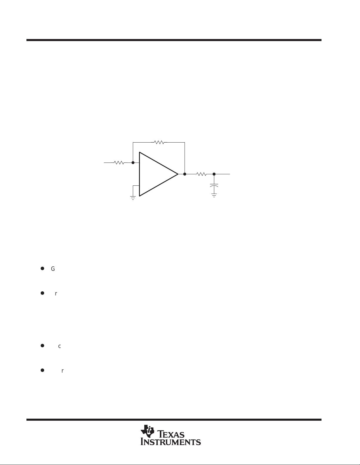
driving a capacitive load
Driving capacitive loads with high performance amplifiers is not a problem as long as certain precautions are
taken. The first is to realize that the THS406x has been internally compensated to maximize its bandwidth and
slew rate performance. When the amplifier is compensated in this manner, capacitive loading directly on the
output will decrease the device’s phase margin leading to high frequency ringing or oscillations. Therefore, for
capacitive loads of greater than 10 pF, it is recommended that a resistor be placed in series with the output of
the amplifier, as shown in Figure 25. A minimum value of 20 Ω should work well for most applications. For
example, in 75-Ω transmission systems, setting the series resistor value to 75 Ω both isolates any capacitance
loading and provides the proper line impedance matching at the source end.
510 Ω
510 Ω
Input
_
THS406x
+
20 Ω
C
LOAD
Output
Figure 25. Driving a Capacitive Load
circuit layout considerations
In order to achieve the levels of high frequency performance of the THS406x, it is essential that proper
printed-circuit board high frequency design techniques be followed. A general set of guidelines is given below.
In addition, a THS406x evaluation board is available to use as a guide for layout or for evaluating the device
performance.
D
Ground planes – It is highly recommended that a ground plane be used on the board to provide all
components with a low inductive ground connection. However, in the areas of the amplifier inputs and
output, the ground plane can be removed to minimize the stray capacitance.
D
Proper power supply decoupling – Use a 6.8-µF tantalum capacitor in parallel with a 0.1-µF ceramic
capacitor on each supply terminal. It may be possible to share the tantalum among several amplifiers
depending on the application, but a 0.1-µF ceramic capacitor should always be used on the supply terminal
of every amplifier. In addition, the 0.1-µF capacitor should be placed as close as possible to the supply
terminal. As this distances increases, the inductance in the connecting trace makes the capacitor less
effective. The designer should strive for distances of less than 0.1 inches between the device power
terminals and the ceramic capacitors.
16
D
Sockets – Sockets are not recommended for high-speed operational amplifiers. The additional lead
inductance in the socket pins will often lead to stability problems. Surface-mount packages soldered directly
to the printed-circuit board is the best implementation.
D
Short trace runs/compact part placements – Optimum high frequency performance is achieved when stray
series inductance has been minimized. To realize this, the circuit layout should be made as compact as
possible thereby minimizing the length of all trace runs. Particular attention should be paid to the inverting
input of the amplifier. Its length should be kept as short as possible. This will help to minimize stray
capacitance at the input of the amplifier.
POST OFFICE BOX 655303 • DALLAS, TEXAS 75265
Page 17

THS4061, THS4062
180-MHz HIGH-SPEED AMPLIFIERS
SLOS234D – DECEMBER 1998 – REVISED FEBRUARY 2000
APPLICATION INFORMATION
circuit layout considerations (continued)
D
Surface-mount passive components – Using surface-mount passive components is recommended for
high-frequency amplifier circuits for several reasons. First, because of the extremely low lead inductance
of surface-mount components, the problem with stray series inductance is greatly reduced. Second, the
small size of surface-mount components naturally leads to a more compact layout, thereby minimizing both
stray inductance and capacitance. If leaded components are used, it is recommended that the lead lengths
be kept as short as possible.
evaluation board
An evaluation board is available for the THS4061 (literature number SLOP226) and THS4062 (literaure number
SLOP235). This board has been configured for very low parasitic capacitance in order to realize the full
performance of the amplifier. A schematic of the evaluation board is shown in Figure 26. The circuitry has been
designed so that the amplifier may be used in either an inverting or noninverting configuration. To order the
evaluation board contact your local TI sales office or distributor. For more detailed information, refer to the
THS4061 EVM User’s Manual
number SLOU040)
(literature number SLOU038) or the
VCC+
THS4062 EVM User’s Manual
(literature
IN+
IN–
R3
49.9 Ω
R2
1 kΩ
R1
49.9 Ω
C3
0.1 µF
R4
1 kΩ
C4
0.1 µF
+
THS4061
_
VCC–
+
NULL
NULL
+
C2
6.8 µF
R5
49.9 Ω
OUT
C1
6.8 µF
Figure 26. THS4061 Evaluation Board Schematic
POST OFFICE BOX 655303 • DALLAS, TEXAS 75265
17
Page 18

THS4061, THS4062
180-MHz HIGH-SPEED AMPLIFIERS
SLOS234D – DECEMBER 1998 – REVISED FEBRUARY 2000
MECHANICAL INFORMATION
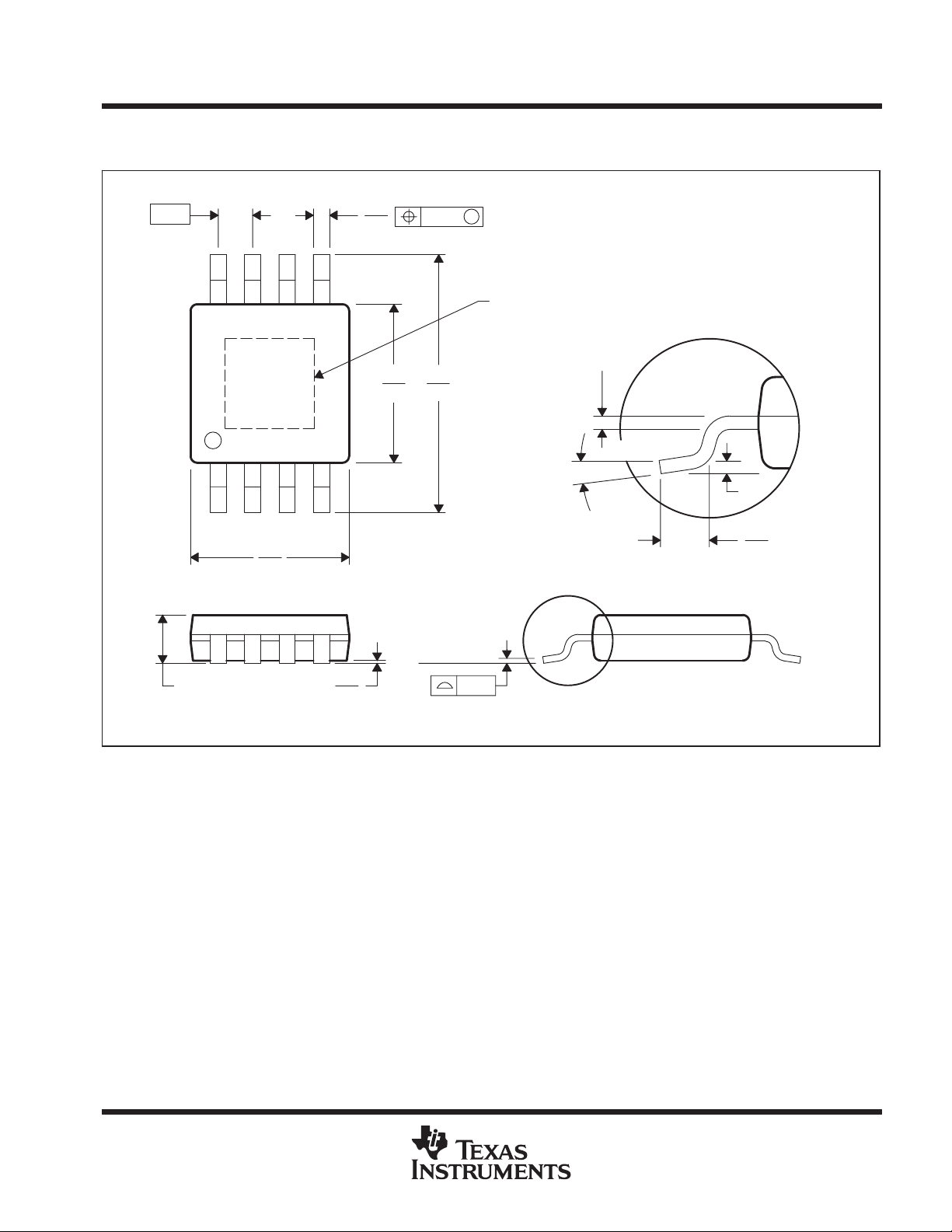
D (R-PDSO-G**) PLASTIC SMALL-OUTLINE PACKAGE
14 PIN SHOWN
14
1
0.069 (1,75) MAX
0.050 (1,27)
A
0.020 (0,51)
0.014 (0,35)
0.010 (0,25)
0.004 (0,10)
8
7
0.010 (0,25)
0.157 (4,00)
0.150 (3,81)
M
0.244 (6,20)
0.228 (5,80)
Seating Plane
0.004 (0,10)
PINS **
DIM
A MAX
A MIN
0.008 (0,20) NOM
Gage Plane
0°–8°
8
0.197
(5,00)
0.189
(4,80)
14
0.344
(8,75)
0.337
(8,55)
0.010 (0,25)
0.044 (1,12)
0.016 (0,40)
4040047/D 10/96
16
0.394
(10,00)
0.386
(9,80)
NOTES: A. All linear dimensions are in inches (millimeters).
B. This drawing is subject to change without notice.
C. Body dimensions do not include mold flash or protrusion, not to exceed 0.006 (0,15).
D. Falls within JEDEC MS-012
18
POST OFFICE BOX 655303 • DALLAS, TEXAS 75265
Page 19
THS4061, THS4062
180-MHz HIGH-SPEED AMPLIFIERS
SLOS234D – DECEMBER 1998 – REVISED FEBRUARY 2000
MECHANICAL INFORMATION
DGN (S-PDSO-G8) PowerPAD PLASTIC SMALL-OUTLINE PACKAGE
0,65
8
1
1,07 MAX
3,05
2,95
0,38
0,25
5
3,05
2,95
4
Seating Plane
0,15
0,05
0,25
4,98
4,78
M
0,10
Thermal Pad
(See Note D)
0,15 NOM
0°–6°
Gage Plane
0,25
0,69
0,41
NOTES: A. All linear dimensions are in millimeters.
B. This drawing is subject to change without notice.
C. Body dimensions include mold flash or protrusions.
D. The package thermal performance may be enhanced by attaching an external heat sink to the thermal pad. This pad is electrically
and thermally connected to the backside of the die and possibly selected leads.
E. Falls within JEDEC MO-187
PowerPAD is a trademark of Texas Instruments Incorporated.
4073271/A 01/98
POST OFFICE BOX 655303 • DALLAS, TEXAS 75265
19
Page 20
THS4061, THS4062
180-MHz HIGH-SPEED AMPLIFIERS
SLOS234D – DECEMBER 1998 – REVISED FEBRUARY 2000
MECHANICAL INFORMATION
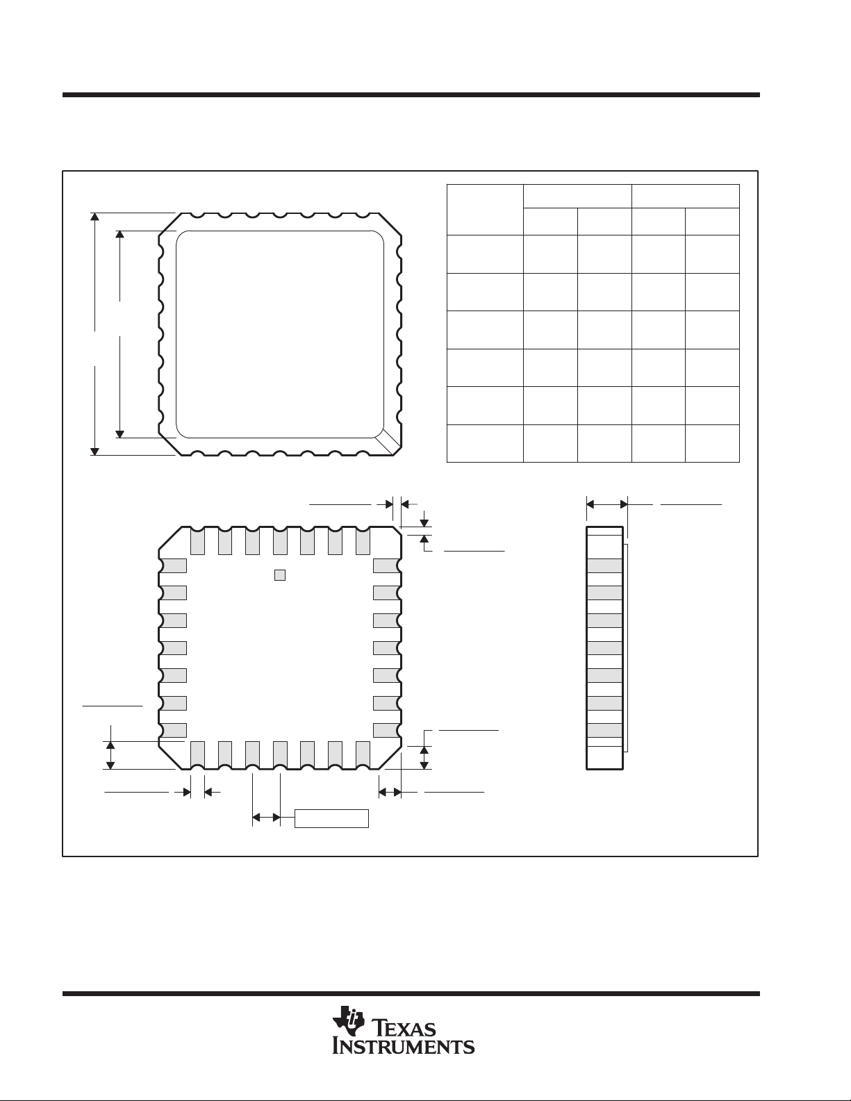
FK (S-CQCC-N**) LEADLESS CERAMIC CHIP CARRIER
28 TERMINAL SHOWN
A SQ
B SQ
20
22
23
24
25
19
21
12826 27
12
1314151618 17
0.020 (0,51)
0.010 (0,25)
MIN
0.342
(8,69)
0.442
0.640
0.739
0.938
1.141
A
(11,63)
(16,76)
(19,32)(18,78)
(24,43)
(29,59)
0.358
(9,09)
0.458
(10,31)
0.660
(12,58)
0.761
(12,58)
0.962
1.165
NO. OF
TERMINALS
**
11
10
9
8
7
6
5
432
20
28
44
52
68
84
0.020 (0,51)
0.010 (0,25)
(11,23)
(16,26)
(23,83)
(28,99)
MINMAX
0.307
(7,80)
0.406
0.495
0.495
0.850
(21,6)
1.047
(26,6)
0.080 (2,03)
0.064 (1,63)
B
MAX
0.358
(9,09)
0.458
(11,63)
0.560
(14,22)
0.560
(14,22)
0.858
(21,8)
1.063
(27,0)
0.055 (1,40)
0.045 (1,14)
0.028 (0,71)
0.022 (0,54)
0.050 (1,27)
NOTES: A. All linear dimensions are in inches (millimeters).
20
B. This drawing is subject to change without notice.
C. This package can be hermetically sealed with a metal lid.
D. The terminals are gold plated.
E. Falls within JEDEC MS-004
POST OFFICE BOX 655303 • DALLAS, TEXAS 75265
0.045 (1,14)
0.035 (0,89)
0.045 (1,14)
0.035 (0,89)
4040140/D 10/96
Page 21

THS4061, THS4062
180-MHz HIGH-SPEED AMPLIFIERS
SLOS234D – DECEMBER 1998 – REVISED FEBRUARY 2000
MECHANICAL INFORMATION
JG (R-GDIP-T8) CERAMIC DUAL-IN-LINE PACKAGE
0.400 (10,20)
0.355 (9,00)
0.063 (1,60)
0.015 (0,38)
0.100 (2,54)
8
1
5
4
0.065 (1,65)
0.045 (1,14)
0.020 (0,51) MIN
0.280 (7,11)
0.245 (6,22)
0.200 (5,08) MAX
0.130 (3,30) MIN
0.023 (0,58)
0.015 (0,38)
0.310 (7,87)
0.290 (7,37)
Seating Plane
0°–15°
0.014 (0,36)
0.008 (0,20)
NOTES: A. All linear dimensions are in inches (millimeters).
B. This drawing is subject to change without notice.
C. This package can be hermetically sealed with a ceramic lid using glass frit.
D. Index point is provided on cap for terminal identification only on press ceramic glass frit seal only.
E. Falls within MIL-STD-1835 GDIP1-T8
POST OFFICE BOX 655303 • DALLAS, TEXAS 75265
4040107/C 08/96
21
Page 22

IMPORTANT NOTICE
T exas Instruments and its subsidiaries (TI) reserve the right to make changes to their products or to discontinue
any product or service without notice, and advise customers to obtain the latest version of relevant information
to verify, before placing orders, that information being relied on is current and complete. All products are sold
subject to the terms and conditions of sale supplied at the time of order acknowledgement, including those
pertaining to warranty, patent infringement, and limitation of liability.
TI warrants performance of its semiconductor products to the specifications applicable at the time of sale in
accordance with TI’s standard warranty. Testing and other quality control techniques are utilized to the extent
TI deems necessary to support this warranty . Specific testing of all parameters of each device is not necessarily
performed, except those mandated by government requirements.
CERTAIN APPLICA TIONS USING SEMICONDUCT OR PRODUCTS MAY INVOLVE POTENTIAL RISKS OF
DEATH, PERSONAL INJURY, OR SEVERE PROPERTY OR ENVIRONMENTAL DAMAGE (“CRITICAL
APPLICATIONS”). TI SEMICONDUCTOR PRODUCTS ARE NOT DESIGNED, AUTHORIZED, OR
WARRANTED TO BE SUITABLE FOR USE IN LIFE-SUPPORT DEVICES OR SYSTEMS OR OTHER
CRITICAL APPLICA TIONS. INCLUSION OF TI PRODUCTS IN SUCH APPLICATIONS IS UNDERST OOD TO
BE FULLY AT THE CUSTOMER’S RISK.
In order to minimize risks associated with the customer’s applications, adequate design and operating
safeguards must be provided by the customer to minimize inherent or procedural hazards.
TI assumes no liability for applications assistance or customer product design. TI does not warrant or represent
that any license, either express or implied, is granted under any patent right, copyright, mask work right, or other
intellectual property right of TI covering or relating to any combination, machine, or process in which such
semiconductor products or services might be or are used. TI’s publication of information regarding any third
party’s products or services does not constitute TI’s approval, warranty or endorsement thereof.
Copyright 2000, Texas Instruments Incorporated
 Loading...