

THS0842
DUAL-INPUT, 8-BIT, 40 MSPS LOW-POWER ANALOG-TO-DIGITAL CONVERTER
WITH SINGLE OR DUAL PARALLEL BUS OUTPUT
SLAS246 – DECEMBER 1999
1
POST OFFICE BOX 655303 • DALLAS, TEXAS 75265
features
D
Dual Simultaneous Sample and Hold Inputs
D
Differential or Single-Ended Analog Inputs
D
8-Bit Resolution 40 MSPS Sampling
Analog-to-Digital Converter (ADC)
D
Single or Dual Parallel Bus Output
D
Low Power Consumption: 275 mW Typ
Using External References
D
Wide Analog Input Bandwidth: 600 MHz Typ
D
3.3 V Single-Supply Operation
D
3.3 V TTL/CMOS-Compatible Digital I/O
D
Internal or External Bottom and Top
Reference V oltages
D
Adjustable Reference Input Range
D
Power-Down (Standby) Mode
D
48-Pin Thin Quad Flat Pack (TQFP)
Package
applications
D
Digital Communications (Baseband
Sampling)
D
Cable Modems
D
Set Top Boxes
D
Test Instruments
description
The THS0842 is a dual 8-bit 40 MSPS high-speed A/D converter. It alternately converts each analog input signal
into 8-bit binary-coded digital words up to a maximum sampling rate of 40 MSPS with an 80 MHz clock. All digital
inputs and outputs are 3.3 V TTL/CMOS-compatible.
Thanks to an innovative single-pipeline architecture implemented in a CMOS process and the 3.3 V supply, the
device consumes very little power. In order to provide maximum flexibility, both bottom and top voltage
references can be set from user supplied voltages. Alternately , if no external references are available, on-chip
references can be used which are also made available externally . The full-scale range is 1 Vpp, depending on
the analog supply voltage. If external references are available, the internal references can be powered down
independently from the rest of the chip, resulting in an even greater power saving.
The device is specifically suited for the baseband sampling of wireless local loop (WLL) communication, cable
modems, set top boxes (STBs), and test instruments.
AVAILABLE OPTIONS
PACKAGED DEVICES
T
A
TQFP-48
–40°C to 85°C THS0842IPFB
PRODUCTION DATA information is current as of publication date.
Products conform to specifications per the terms of Texas Instruments
standard warranty. Production processing does not necessarily include
testing of all parameters.
Please be aware that an important notice concerning availability, standard warranty, and use in critical applications of
Texas Instruments semiconductor products and disclaimers thereto appears at the end of this data sheet.
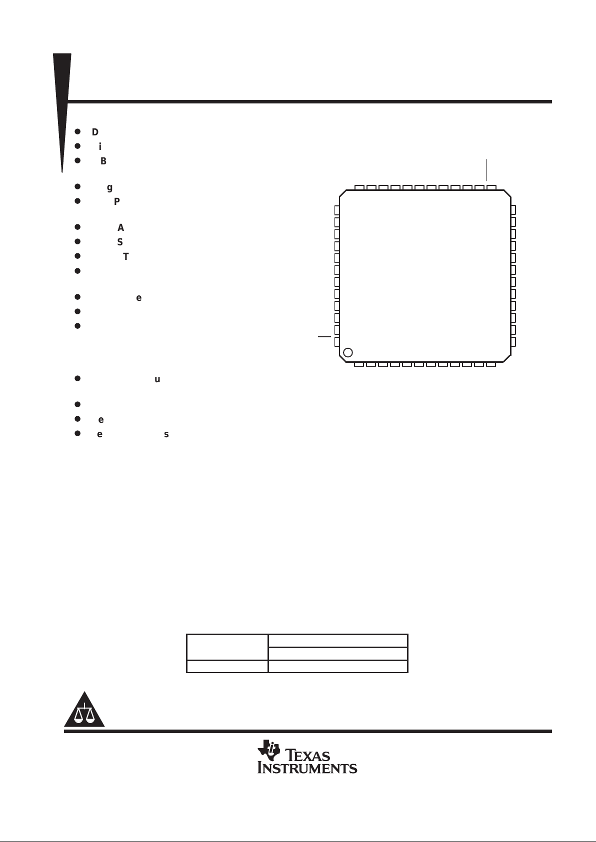
23
DRV
SS
DA0
DA1
DA2
DA3
DA4
DA5
DA6
DA7
NC
NC
DRV
DD
24
23
22
21
20
19
18
17
16
15
14
13
4
37
38
39
40
41
42
43
44
45
46
47
48
AV
DD
I+
I–
AV
SS
AV
DD
STBY
DV
SS
SELB
DV
DD
AV
SS
CLK
OE
5678
BGAVAV
C
35 34 33 32 3136 30
AVQ–Q+
PWDN_REF
CML
DB1
DB0
SS
NC
DB6
DB5
DB4
DB3
DB2
28 27 2629
9
10 11 12
25
1
C
REFT
REFB
NC
DD
DB7
PFB PACKAGE
(TOP VIEW)
DRV
DRV
SS
DD
OUT
SS
OUT
Copyright 1999, Texas Instruments Incorporated
THS0842
DUAL-INPUT, 8-BIT, 40 MSPS LOW-POWER ANALOG-TO-DIGITAL CONVERTER
WITH SINGLE OR DUAL PARALLEL BUS OUTPUT
SLAS246 – DECEMBER 1999
2
POST OFFICE BOX 655303 • DALLAS, TEXAS 75265
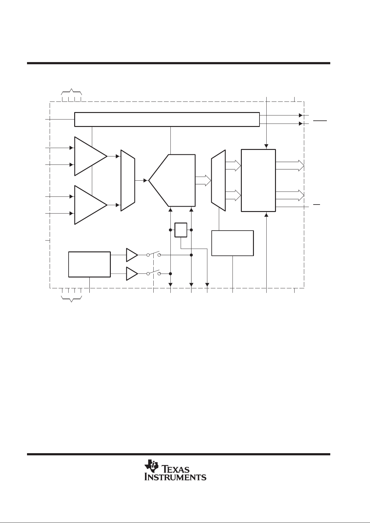
functional block diagram
MUX
Sample
& Hold
Sample
& Hold
BUS
MUX
8 BIT
ADC
3-State
Output
Buffers
Configuration
Control
Circuit
OE
DA(7–0)
I +
I –
Q +
Q –
STBY
CLK
CM
Internal
Reference
Circuit
REFT REFB CML
PWDN
REF
SELB DRV
SS
DV
SS
DRV
DD
DV
DD
Timing Circuitry
AV
SS
AV
DD
C
OUT
C
OUT
BG
DB(7–0)
THS0842
DUAL-INPUT, 8-BIT, 40 MSPS LOW-POWER ANALOG-TO-DIGITAL CONVERTER
WITH SINGLE OR DUAL PARALLEL BUS OUTPUT
SLAS246 – DECEMBER 1999
3
POST OFFICE BOX 655303 • DALLAS, TEXAS 75265
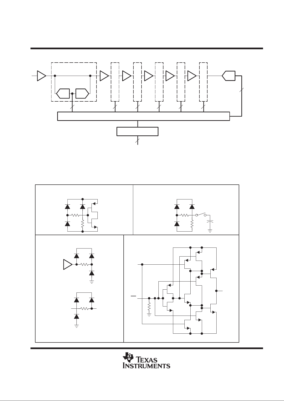
ADC pipeline block diagram
SHA
DACADC
+
–
ADC
Correction Logic
Output Buffers
2222 2
D0(LSB)–D7(MSB)
2
2
SHA SHA SHA SHA SHA
The single-pipeline architecture uses 6 ADC/DAC stages and one final flash ADC. Each stage produces a
resolution of 2 bits. Digital correction logic generates its result using the 2-bit result from the first stage, 1 bit from
each of the 5 succeeding stages, and 1 bit from the final stage in order to arrive at an 8-bit result. The correction
logic ensures no missing codes over the full operating temperature range.
circuit diagrams of inputs and outputs
DV
DD
AV
DD
AV
DD
0.5 pF
Internal
Reference
Generator
REFTO
or
REFBO
AV
DD
REFBI
or
REFTI
OE
ALL DIGITAL INPUT CIRCUITS AIN INPUT CIRCUIT
REFERENCE INPUT CIRCUIT D0–D7 OUTPUT CIRCUIT
DRV
DD
DRV
SS
D_Out
D
THS0842
DUAL-INPUT, 8-BIT, 40 MSPS LOW-POWER ANALOG-TO-DIGITAL CONVERTER
WITH SINGLE OR DUAL PARALLEL BUS OUTPUT
SLAS246 – DECEMBER 1999
4
POST OFFICE BOX 655303 • DALLAS, TEXAS 75265
Terminal Functions
TERMINAL
NAME NO.
I/O
DESCRIPTION
AV
DD
27, 37, 41 I Analog supply voltage
AV
SS
28, 36, 40,46I Analog ground
BG 29 O Band gap reference voltage. A 1-µF capacitor with a 0.1-µF capacitor in parallel should be connected
between this terminal and A VSS for external filtering.
CLK 47 I Clock input. The input is sampled on each rising edge of CLK.
CML 32 O Common mode level. This voltage is equal to (A VDD – AVSS)/2. An external 1-µF capacitor with a 0.1-µF
capacitor in parallel should be connected between this terminal and AVSS.
C
OUT
26 O Latch clock for the data outputs
C
OUT
25 O Inverted latch clock for the data outputs
DB7 – DB0 4 – 11 O Data outputs. D7 is the MSB. This is the second bus. Data is output from the Q channel when dual bus
output mode is selected. Pin SELB selects the output mode.
DRV
DD
1, 13 I Supply voltage for output drivers
DRV
SS
12, 24 I Ground for digital output drivers
DA7 – DA0 16 – 23 I Data outputs for bus A. D7 is MSB. This is the primary bus. Data from both input channels can be output
on this bus or data from the I channel only. Pin SELB selects the output mode.
DV
DD
45 I Digital supply voltage
DV
SS
43 I Digital ground
I– 39 I Negative input for analog channel 0.
I+ 38 I Positive input for analog channel 0.
NC 2,3,14,15 No connect. Reserved for future use
OE 48 I Output enable. A high on this terminal will disable the output bus.
PWDN_REF 33 I Power down for internal reference voltages. A high on this terminal will disable the internal reference
circuit.
Q– 35 I Negative input for analog channel 1
Q+ 34 I Positive input for analog channel 1
REFB 30 I/O Reference voltage bottom. The voltage at this terminal defines the bottom reference voltage for the ADC.
Sufficient filtering should be applied to this input. A 1-µF capacitor with a 0.1-µF capacitor in parallel should
be connected between REFB and AVSS. Additionally , a 0.1-µF capacitor can be connected between REFT
and REFB.
REFT 31 I/O Reference voltage top. The voltage at this terminal defines the top reference voltage for the ADC. Sufficient
filtering should be applied to this input. A 1-µF capacitor with a 0.1-µF capacitor in parallel should be
connected between REFT and AVSS. Additionally , a 0.1-µF capacitor can be connected between REFT
and REFB.
SELB 44 I Selects either single bus or data output or dual bus output data output. A low selects dual bus data output.
STBY 42 I Standby input. A high level on this terminal will power down the device.
THS0842
DUAL-INPUT, 8-BIT, 40 MSPS LOW-POWER ANALOG-TO-DIGITAL CONVERTER
WITH SINGLE OR DUAL PARALLEL BUS OUTPUT
SLAS246 – DECEMBER 1999
5
POST OFFICE BOX 655303 • DALLAS, TEXAS 75265
absolute maximum ratings over operating free-air temperature (unless otherwise noted)
†
Supply voltage: AVDD to AGND, DVDD to DGND –0.5 V to 4 V. . . . . . . . . . . . . . . . . . . . . . . . . . . . . . . . . . . . . .
Supply voltage: AVDD to DVDD, AGND to DGND –0.5 V to 0.5 V. . . . . . . . . . . . . . . . . . . . . . . . . . . . . . . . . . . . .
Digital input voltage range to DGND –0.5 V to DV
DD
+ 0.5 V. . . . . . . . . . . . . . . . . . . . . . . . . . . . . . . . . . . . . . . . .
Analog input voltage range to AGND –0.5 V to AVDD + 0.5 V. . . . . . . . . . . . . . . . . . . . . . . . . . . . . . . . . . . . . . . .
Digital output voltage applied from external source to DGND –0.5 V to DVDD + 0.5 V. . . . . . . . . . . . . . . . . . .
Reference voltage input range to AGND: V
(REFT)
, V
(REFB)
–0.5 V to AVDD + 0.5 V. . . . . . . . . . . . . . . . . . . .
Operating free-air temperature range, TA: –40°C to 85°C. . . . . . . . . . . . . . . . . . . . . . . . . . . . . . . . . . . . . . . . . .
Storage temperature range, T
stg
–55°C to 150°C. . . . . . . . . . . . . . . . . . . . . . . . . . . . . . . . . . . . . . . . . . . . . . . . . . .
†
Stresses beyond those listed under “absolute maximum ratings” may cause permanent damage to the device. These are stress ratings only, and
functional operation of the device at these or any other conditions beyond those indicated under “recommended operating conditions” is not
implied. Exposure to absolute-maximum-rated conditions for extended periods may affect device reliability.
recommended operating conditions over operating free-air temperature range
power supply
MIN NOM MAX UNIT
AV
DD
Supply voltage
DV
DD
3 3.3 3.6 V
DRV
DD
analog and reference inputs
MIN NOM MAX UNIT
Reference input voltage (top), V
(REFT)
(NOM) – 0.2 AVDD – 1 (NOM) + 0.2 V
Reference input voltage (bottom), V
(REFB)
0.8 1 1.2 V
Reference voltage differential, V
(REFT)
– V
(REFB)
AVDD – 2 V
Analog input voltage, V
(IN)
V
(REFB)
V
(REFT)
V
digital inputs
MIN NOM MAX UNIT
High-level input voltage, V
IH
2.0 DV
DD
V
Low-level input voltage, V
IL
DGND 0.2xDV
DD
V
Clock period, t
c
12.5 ns
Pulse duration, clock high, t
w(CLKH)
5.25 ns
Pulse duration, clock low, t
w(CLKL)
5.25 ns
THS0842
DUAL-INPUT, 8-BIT, 40 MSPS LOW-POWER ANALOG-TO-DIGITAL CONVERTER
WITH SINGLE OR DUAL PARALLEL BUS OUTPUT
SLAS246 – DECEMBER 1999
6
POST OFFICE BOX 655303 • DALLAS, TEXAS 75265
electrical characteristics over recommended operating conditions with f
CLK
= 80 MSPS and use
of internal voltage references, AV
DD
= DVDD = DRVDD = 3 V , TA = –40°C to 80°C, dual output bus mode
(unless otherwise noted)
power supply
PARAMETER TEST CONDITIONS MIN TYP MAX UNIT
AV
DD
73 95
I
DD
Operating supply current
DV
DD
AVDD = DVDD = DRVDD = 3.3 V,
p
–
3 3.8
mA
DRV
DD
C
L
= 15 F,
V
I
= 1
MHz
, –1
dBFS
17 22
p
PWDN_REF = L 320 393
PDPower dissipation
PWDN_REF = H 275 335
mW
P
D(STBY)
Standby power STBY = H, CLK held high or low 11 15
logic inputs
PARAMETER TEST CONDITIONS MIN TYP MAX UNIT
I
IH
High-level input current on CLK
†
AVDD = DVDD = DRVDD = CLK = 3.6 V 10 µA
I
IL
Low-level input current on digital inputs
(OE
, STDBY, PWDN_REF, CLK)
AVDD = DVDD = DRVDD = 3.6 V,
Digital inputs at 0 V
10 µA
CIInput capacitance 5 pF
†
IIH leakage current on other digital inputs (OE
, STDBY , PWDN_REF) is not measured since these inputs have an internal pull-down resistor of
4 KΩ to DGND.
logic outputs
PARAMETER TEST CONDITIONS MIN TYP MAX UNIT
V
OH
High-level output voltage
AVDD = DVDD = DRVDD = 3 V at IOH = 50 µA,
Digital output forced high
2.8 V
V
OL
Low-level output voltage
AVDD = DVDD = DRVDD = 3.6 V at IOL = 50 µA,
Digital output forced low
0.1 V
C
O
Output capacitance 5 pF
I
OZH
High-impedance state output current to
high level
10 µA
I
OZL
High-impedance state output current to
low level
AV
DD
=
DV
DD
=
DRV
DD
= 3.6
V
10 µA
THS0842
DUAL-INPUT, 8-BIT, 40 MSPS LOW-POWER ANALOG-TO-DIGITAL CONVERTER
WITH SINGLE OR DUAL PARALLEL BUS OUTPUT
SLAS246 – DECEMBER 1999
7
POST OFFICE BOX 655303 • DALLAS, TEXAS 75265
electrical characteristics over recommended operating conditions with f
CLK
= 80 MSPS and use
of internal voltage references, AV
DD
= DVDD = DRVDD = 3 V , TA = –40°C to 80°C, dual output bus mode
(unless otherwise noted) (continued)
dc accuracy
PARAMETER TEST CONDITIONS MIN TYP MAX UNIT
Integral nonlinearity (INL), best-fit See Note 1 TA = –40°C to 85°C –2.2 ±1.5 2.2 LSB
Differential nonlinearity (DNL) See Note 2 TA = –40°C to 85°C –1 ±0.7 2 LSB
Offset error
°
°
±0.1 5 %FS
Gain error
T
A
= –
40°C to 85°C, (see Note 3)
±7.1 %FS
Offset match TA = –40°C to 85°C, (see Note 4) –1 ±0.1 1 LSB
Gain match TA = –40°C to 85°C, (see Note 5) –5 1 LSB
Missing codes – no missing codes assured
NOTES: 1. Integral nonlinearity refers to the deviation of each individual code from a line drawn from zero to full scale. The point used as zero
occurs 1/2 LSB before the first code transition. The full–scale point is defined as a level 1/2 LSB beyond the last code transition.
The deviation is measured from the center of each particular code to the best fit line between these two endpoints.
2. An ideal ADC exhibits code transitions that are exactly 1 LSB apart. DNL is the deviation from this ideal value. Therefore this measure
indicates how uniform the transfer function step sizes are. The ideal step size is defined here as the step size for the device under
test (i.e., (last transition level – first transition level) ÷ (2n – 2)). Using this definition for DNL separates the effects of gain and offset
error. A minimum DNL better than –1 LSB ensures no missing codes.
3. Offset error is defined as the difference in analog input voltage – between the ideal voltage and the actual voltage – that will switch
the ADC output from code 0 to code 1. The ideal voltage level is determined by adding the voltage corresponding to 1/2 LSB to the
bottom reference level. The voltage corresponding to 1 LSB is found from the difference of top and bottom references divided by
the number of ADC output levels (256).
Gain error is defined as the difference in analog input voltage – between the ideal voltage and the actual voltage – that will switch
the ADC output from code 254 to code 255. The ideal voltage level is determined by subtracting the voltage corresponding to 1.5
LSB from the top reference level. The voltage corresponding to 1 LSB is found from the difference of top and bottom references
divided by the number of ADC output levels (256).
4. Offset match is the change in offset error between I and Q channels.
5. Gain match is the change in gain error between I and Q channels.
analog input
PARAMETER TEST CONDITIONS MIN TYP MAX UNIT
C
I
Input capacitance 4 pF
reference input (AVDD = DVDD = DRVDD = 3.6 V)
PARAMETER TEST CONDITIONS MIN TYP MAX UNIT
R
ref
Reference input resistance 200 Ω
I
ref
Reference input current 5 mA
reference outputs
PARAMETER TEST CONDITIONS MIN TYP MAX UNIT
V
(REFT)
Reference top voltage
2 + [(AVDD – 3)/2]
V
(REFB)
Reference bottom voltage
AV
DD
=
3 V
1 + [(AVDD – 3)/2]
V
V
REFB–VREFB
Absolute min/max values valid
and tested for AVDD = 3 V
0.9 1 1.3 V
THS0842
DUAL-INPUT, 8-BIT, 40 MSPS LOW-POWER ANALOG-TO-DIGITAL CONVERTER
WITH SINGLE OR DUAL PARALLEL BUS OUTPUT
SLAS246 – DECEMBER 1999
8
POST OFFICE BOX 655303 • DALLAS, TEXAS 75265
electrical characteristics over recommended operating conditions with f
CLK
= 80 MSPS and use
of internal voltage references, AV
DD
= DVDD = DRVDD = 3 V , TA = –40°C to 80°C, dual output bus mode
(unless otherwise noted) (continued)
dynamic performance
†
PARAMETER TEST CONDITIONS MIN TYP MAX UNIT
fin = 1 MHz 6.6 6.9
Effective number of bits, ENOB
fin = 15 MHz 6.4 6.8
Bits
fin = 20 MHz 6.4 6.8
fin = 1 MHz 41.5 43.5
Signal-to-total harmonic distortion + noise, S/(THD+N)
fin = 15 MHz 40 42.5
dB
fin = 20 MHz 40 42.5
fin = 1 MHz –51 –46
Total harmonic distortion (THD)
fin = 15 MHz –48.5 –44
dB
fin = 20 MHz –48.5 –44
fin = 1 MHz 48 53
Spurious free dynamic range (SFDR)
fin = 15 MHz 47 52.2
dB
fin = 20 MHz 46 52
Analog input full-power bandwidth, BW See Note 6 600 MHz
Intermodulation distortion f1 = 1 MHz, f2 = 1.02 MHz 50 dBc
I/Q channel crosstalk AVDD = DVDD = DRVDD = 3.3 V –52 dBc
†
Based on analog input voltage of –1 dBFS referenced to a 1.3 Vpp full-scale input range.
NOTE 6: The analog input bandwidth is defined as the maximum frequency of a –1 dBFS input sine that can be applied to the device for which
an extra 3 dB attenuation is observed in the reconstructed output signal.
timing requirements
PARAMETER TEST CONDITIONS MIN TYP MAX UNIT
Maximum clock rate (see Note 7) 80 MHz
f
clk
Minimum clock rate 10 kHz
t
d(O)
Output delay time (see timing diagram) CL = 10 pF 9 ns
t
h(O)
Output hold time from C
OUT
or C
OUT
to data invalid 2 ns
p
I data 5.5 5.5 5.5
CLK
t
d(pipe)
Pipeline delay (latency)
Q data 6.5 6.5 6.5
cycles
t
d(a)
Aperture delay time 3 ns
t
j(a)
Aperture jitter 1.5 ps, rms
t
dis
Disable time, OE rising to Hi-Z 5 ns
t
en
Enable time, OE falling to valid data 5 ns
t
su(O)
Output setup time from data to C
OUT
or C
OUT
8 7 ns
NOTE 7: Conversion rate is 1/2 the clock rate, f
clk
.
THS0842
DUAL-INPUT, 8-BIT, 40 MSPS LOW-POWER ANALOG-TO-DIGITAL CONVERTER
WITH SINGLE OR DUAL PARALLEL BUS OUTPUT
SLAS246 – DECEMBER 1999
9
POST OFFICE BOX 655303 • DALLAS, TEXAS 75265
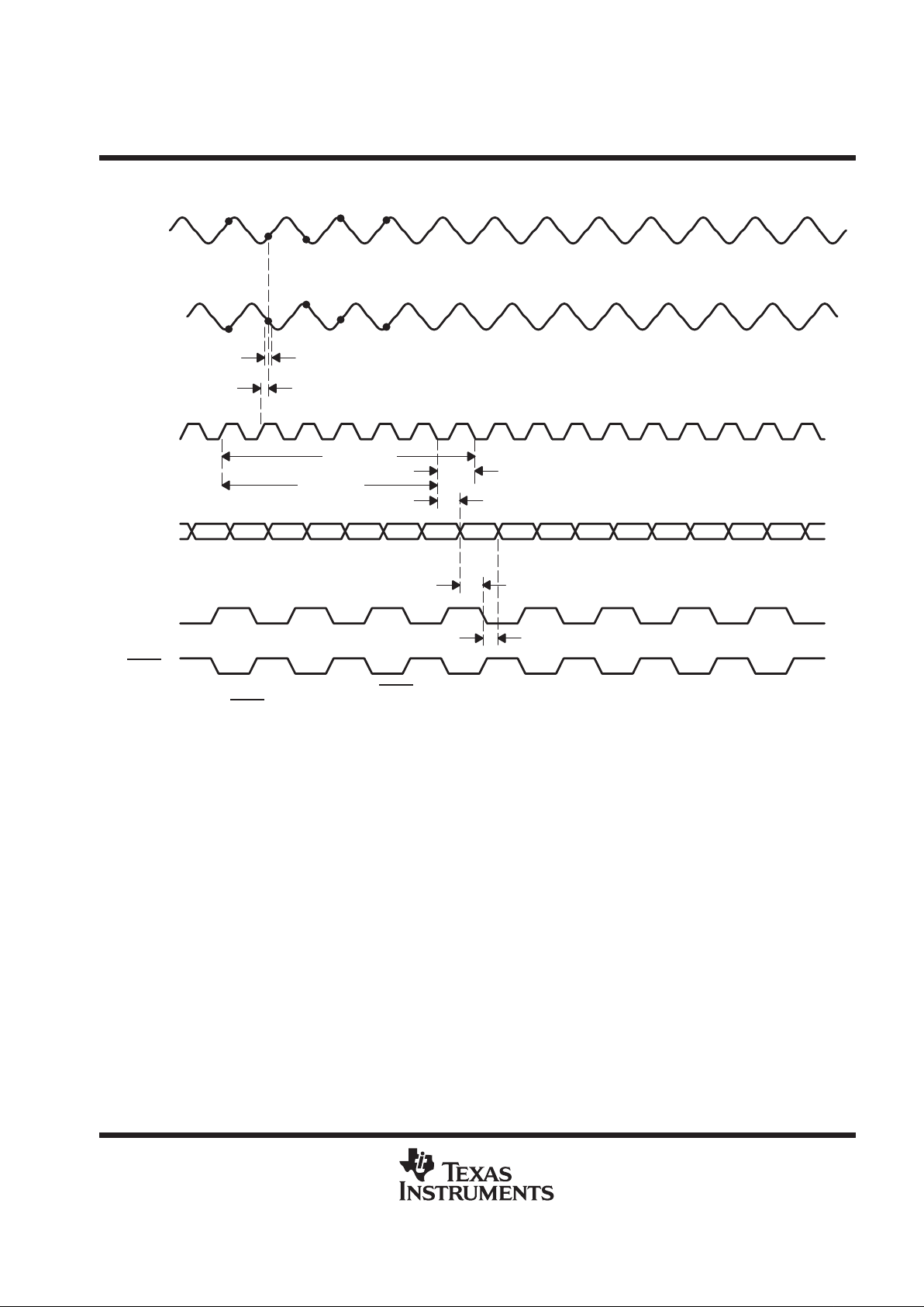
PARAMETER MEASUREMENT INFORMATION
C
OUT
01234567 910118 12131415
I5Q4I4Q3I3Q2I2Q1I1Q–1I–1Q–2I–2Q–3I–3 Q5
DA(7–0)
CLK
Q
I
t
h(O)
t
su(O)
t
d(O)
t
d(pipe-I)
N
N
N+1
N+1
N+2
N+2
N+3
N+3
N+4
N+4
t
d(A)
t
J(A)
t
d(pipe-Q)
t
d(O)
C
OUT
NOTE A: The relationship between CLK and C
OUT/COUT
is not fixed and depends on the power-on conditions. Data out should be referenced
to C
OUT
and C
OUT
.
Figure 1. Timing Diagram, Single Bus Output

THS0842
DUAL-INPUT, 8-BIT, 40 MSPS LOW-POWER ANALOG-TO-DIGITAL CONVERTER
WITH SINGLE OR DUAL PARALLEL BUS OUTPUT
SLAS246 – DECEMBER 1999
10
POST OFFICE BOX 655303 • DALLAS, TEXAS 75265
PARAMETER MEASUREMENT INFORMATION
C
OUT
01234567 910118 12131415
I5
DA(7–0)
CLK
Q
I
t
h
t
su
t
d(pipe-I)
N
N
N+1
N+1
N+2
N+2
N+3
N+3
N+4
N+4
t
d(A)
t
J(A)
16
DAB(15–0)
I4I3I2I1I–1I–2I–3I–4
Q4
DB(7–0)
Q3Q2Q1Q–1Q–2Q–3Q–4 Q5
t
d(0)
DAB(15–0) is the combination of both DA and DB. It illustrates when both buses have valid data for latching.
I3 & Q3 I4 & Q4 I5 & Q5I2 & Q2I1 & Q1
t
d(pipe-Q)
t
d(0)
C
OUT
NOTE A: The relationship between CLK and C
OUT/COUT
is not fixed and depends on the power-on conditions. Data out should be referenced
to C
OUT
and C
OUT
.
Figure 2. Timing Diagram, Dual Bus Output

THS0842
DUAL-INPUT, 8-BIT, 40 MSPS LOW-POWER ANALOG-TO-DIGITAL CONVERTER
WITH SINGLE OR DUAL PARALLEL BUS OUTPUT
SLAS246 – DECEMBER 1999
11
POST OFFICE BOX 655303 • DALLAS, TEXAS 75265
TYPICAL CHARACTERISTICS
†
Figure 3
0
20
40
60
80
100
120
–40 –15
10 35
60 85
ICC Total
IAV
DD
IDRV
DD
IDV
DD
I – Current – mA
POWER CONSUMPTION
vs
TEMPERATURE
TA – Temperature – °C
Figure 4
6
6.1
6.2
6.3
6.4
6.5
6.6
6.7
6.8
6.9
7
0
5
10 15 20
ENOB – Effective Number of Bits – Bits
EFFECTIVE NUMBER OF BITS
vs
ANALOG INPUT FREQUENCY
fi – Analog Input Frequency – MHz
40
41
42
43
44
45
46
47
48
49
50
–40
–15
10 35 60
85
SNR – Signal-to-Noise Ratio – dB
SIGNAL-TO-NOISE RATIO
vs
TEMPERATURE
TA – Temperature –°C
Figure 5
†
Unless otherwise noted AVDD = DVDD = DRVDD = 3 V, f
CLK
= 80 MHz, Analog Input = –1 dB FS, TA = 25°C.

THS0842
DUAL-INPUT, 8-BIT, 40 MSPS LOW-POWER ANALOG-TO-DIGITAL CONVERTER
WITH SINGLE OR DUAL PARALLEL BUS OUTPUT
SLAS246 – DECEMBER 1999
12
POST OFFICE BOX 655303 • DALLAS, TEXAS 75265
TYPICAL CHARACTERISTICS
†
DIFFERENTIAL NONLINEARITY
–2
–1.5
–1
–0.5
0
0.5
1
1.5
2
0
128 255
ADC CODE
DNL – Differential Nonlinerity – LSB
Figure 6
INTEGRAL NONLINEARITY
–2
–1.5
–1
–0.5
0
0.5
1
1.5
2
0
128 255
ADC CODE
INL – Integral Nonlinearity – LSB
Figure 7
–140
–120
–100
–80
–60
–40
–20
0
02468
10
12
14
16
18
20
f – Frequency – MHz
I Input Channel
AIN = 1.1 MHz
Power – dBFS
FAST FOURIER TRANSFORM
Figure 8
†
Unless otherwise noted AVDD = DVDD = DRVDD = 3 V, f
CLK
= 80 MHz, Analog Input = –1 dB FS, TA = 25°C.

THS0842
DUAL-INPUT, 8-BIT, 40 MSPS LOW-POWER ANALOG-TO-DIGITAL CONVERTER
WITH SINGLE OR DUAL PARALLEL BUS OUTPUT
SLAS246 – DECEMBER 1999
13
POST OFFICE BOX 655303 • DALLAS, TEXAS 75265
TYPICAL CHARACTERISTICS
†
–140
–120
–100
–80
–60
–40
–20
0
02468
10
12 14 16 18 20
f – Frequency – MHz
Power – dBFS
Q Input Channel
AIN = 1.1 MHz
FAST FOURIER TRANSFORM
Figure 9
–140
–120
–100
–80
–60
–40
–20
0
0 2 4 6 8 101214161820
f – Frequency – MHz
Power – dBFS
I Input Channel
AIN = 15.1 MHz
FAST FOURIER TRANSFORM
Figure 10
–140
–120
–100
–80
–60
–40
–20
0
0 2 4 6 8 10 12 14 16 18 20
f – Frequency – MHz
FAST FOURIER TRANSFORM
Power – dBFS
Q Input Channel
AIN = 15.1 MHz
Figure 11
†
Unless otherwise noted AVDD = DVDD = DRVDD = 3 V, f
CLK
= 80 MHz, Analog Input = –1 dB FS, TA = 25°C.

THS0842
DUAL-INPUT, 8-BIT, 40 MSPS LOW-POWER ANALOG-TO-DIGITAL CONVERTER
WITH SINGLE OR DUAL PARALLEL BUS OUTPUT
SLAS246 – DECEMBER 1999
14
POST OFFICE BOX 655303 • DALLAS, TEXAS 75265
TYPICAL CHARACTERISTICS
†
–140
–120
–100
–80
–60
–40
–20
0
02468101214161820
f – Frequency – MHz
FAST FOURIER TRANSFORM
Power – dBFS
I Input Channel
AIN = 20 MHz
Figure 12
–140
–120
–100
–80
–60
–40
–20
0
0 2 4 6 8101214161820
f – Frequency – MHz
FAST FOURIER TRANSFORM
Power – dBFS
Q Input Channel
AIN = 20 MHz
Figure 13
†
Unless otherwise noted AVDD = DVDD = DRVDD = 3 V, f
CLK
= 80 MHz, Analog Input = –1 dB FS, TA = 25°C.

THS0842
DUAL-INPUT, 8-BIT, 40 MSPS LOW-POWER ANALOG-TO-DIGITAL CONVERTER
WITH SINGLE OR DUAL PARALLEL BUS OUTPUT
SLAS246 – DECEMBER 1999
15
POST OFFICE BOX 655303 • DALLAS, TEXAS 75265
TYPICAL CHARACTERISTICS
†
–14
–12
–10
–8
–6
–4
–2
0
2
4
1
10
100 1000
f – Frequency – MHz
Power – dB
ANALOG INPUT BANDWIDTH
Figure 14
–120
–100
–80
–60
–40
–20
0
0 0.2 0.4 0.6 0.8 1 1.2 1.4 1.6 1.8 2
f – Frequency – MHz
TWO-TONE INTERMODULATION DISTORTION
Power – dB
f1 = 1 MHz, –7 dBFS
f2 = 1.04 MHz, –7 dBFS
Figure 15
†
Unless otherwise noted AVDD = DVDD = DRVDD = 3 V, f
CLK
= 80 MHz, Analog Input = –1 dB FS, TA = 25°C.

THS0842
DUAL-INPUT, 8-BIT, 40 MSPS LOW-POWER ANALOG-TO-DIGITAL CONVERTER
WITH SINGLE OR DUAL PARALLEL BUS OUTPUT
SLAS246 – DECEMBER 1999
16
POST OFFICE BOX 655303 • DALLAS, TEXAS 75265
TYPICAL CHARACTERISTICS
†
–110
–100
–90
–80
–70
–60
–50
–40
–30
–20
–10
0
0 2 4 6 8 101214161820
f – Frequency – MHz
I CHANNEL CROSSTALK
SNR – Signal-to-Noise Ratio – dB
Figure 16
–110
–100
–90
–80
–70
–60
–50
–40
–30
–20
–10
0
0 2 4 6 8 101214161820
f – Frequency – MHz
Q CHANNEL CROSSTALK
SNR – Signal-to-Noise Ratio – dB
Figure 17
†
Unless otherwise noted AVDD = DVDD = DRVDD = 3 V, f
CLK
= 80 MHz, Analog Input = –1 dB FS, TA = 25°C.

THS0842
DUAL-INPUT, 8-BIT, 40 MSPS LOW-POWER ANALOG-TO-DIGITAL CONVERTER
WITH SINGLE OR DUAL PARALLEL BUS OUTPUT
SLAS246 – DECEMBER 1999
17
POST OFFICE BOX 655303 • DALLAS, TEXAS 75265
PRINCIPLES OF OPERATION
definitions of specifications and terminology
integral nonlinearity (INL)
Integral nonlinearity refers to the deviation of each individual code from a line drawn from zero through full scale.
The point used as zero occurs 1/2 LSB before the first code transition. The full-scale point is defined as level
1/2 LSB beyond the last code transition. The deviation is measured from the center of each particular code to
the true straight line between these two endpoints.
differential nonlinearity (DNL)
An ideal ADC exhibits code transitions that are exactly 1 LSB apart. DNL is the deviation from this ideal value.
Therefore this measure indicates how uniform the transfer function step sizes are. The ideal step size is defined
here as the step size for the device under test, i.e. (last transition level – first transition level)/(2n –2). Using this
definition for DNL separates the effects of gain and offset error. A minimum DNL better than –1 LSB ensures
no missing codes.
offset and gain error
Offset error is defined as the difference in analog input voltage – between the ideal voltage and the actual voltage
– that will switch the ADC output from code 0 to code 1. The ideal voltage level is determined by adding the
voltage corresponding to 1/2 LSB to the bottom reference level. The voltage corresponding to 1 LSB is found
from the difference of top and bottom references divided by the number of ADC output levels (256).
Gain error is defined as the difference in analog input voltage – between the ideal voltage and the actual voltage
– that will switch the ADC output from code 254 to code 255. The ideal voltage level is determined by subtracting
the voltage corresponding to 1.5 LSB from the top reference level. The voltage corresponding to 1 LSB is found
from the difference of top and bottom references divided by the number of ADC output levels (256).
analog input bandwidth
The analog input bandwidth is defined as the maximum frequency of a 1-dBFS input sine wave that can be
applied to the device for which an extra 3-dB attenuation is observed in the reconstructed output signal.
output timing
Output timing t
d(o)
is measured from the 1.5-V level of the CLK input falling edge to the 10%/90% level of the
digital output. The digital output load is not higher than 10 pF.
Output hold time t
h(o)
is measured from the 1.5-V level of the CLK input falling edge to the10%/90% level of the
digital output. The digital output load is not less than 2 pF.
Aperture delay t
d(A)
is measured from the 1.5-V level of the CLK input to the actual sampling instant.
The OE signal is asynchronous.
OE timing t
dis
is measured from the V
IH(min)
level of OE to the high-impedance state of the output data. The
digital output load is not higher than 10 pF.
OE timing ten is measured from the V
IL(max)
level of OE to the instant when the output data reaches V
OH(min)
or V
OL(max)
output levels. The digital output load is not higher than 10 pF.

THS0842
DUAL-INPUT, 8-BIT, 40 MSPS LOW-POWER ANALOG-TO-DIGITAL CONVERTER
WITH SINGLE OR DUAL PARALLEL BUS OUTPUT
SLAS246 – DECEMBER 1999
18
POST OFFICE BOX 655303 • DALLAS, TEXAS 75265
PRINCIPLES OF OPERATION
definitions of specifications and terminology (continued)
pipeline delay (latency)
The number of clock cycles between conversion initiation on an input sample and the corresponding output data
being made available from the ADC pipeline. Once the data pipeline is full, new valid output data is provided
on every clock cycle. In order to know when data is stable on the output pins, the output delay time t
d(o)
(i.e.,
the delay time through the digital output buffers) needs to be added to the pipeline latency . Note that since the
max t
d(o)
is more than 1/2 clock period at 80 MHz, data cannot be reliably clocked in on a rising edge of CLK
at this speed. The falling edge should be used.
The THS0842 implements a high-speed 40 MSPS converter in a cost effective CMOS process. Powered from
3.3 V , the single pipeline design architecture ensures low power operation and 8-bit accuracy . Signal inputs are
differential and the clock signal is single ended. The digital inputs are 3.3 V TTL/CMOS compatible. Internal
voltage references are included for both bottom and top voltages. Therefore, the converter forms a
self-contained solution. Alternatively , the user may apply externally generated reference voltages. In doing so,
both input offset and input range can be modified to suit the application.
The analog input signal is captured by a high speed sampling and hold. Multiple stages will generate the output
code with a pipeline delay of 6.5 CLK cycles. Correction logic combines the multistage data and aligns the 8-bit
output word. All digital logic operates at the rising edge of CLK.
analog input
C
I
R
SW
R
S
VS+
THS0842
+
–
+
–
C
I
VS–
R
SW
R
S
V
CM
V
CM
Figure 18. Simplified Equivalent Input Circuit
A first-order approximation for the equivalent analog input circuit of the THS0842 is shown in Figure 18. The
equivalent input capacitance CI is 5 pF typical. The input must charge/discharge this capacitance within the
sample period of one half of a clock cycle. When a full-scale voltage step is applied, the input source provides
the charging current through the switch resistance R
SW
(200 Ω) of S1 and quickly settles. In this case the input
impedance is low. Alternatively, when the source voltage equals the value previously stored on CI, the hold
capacitor requires no input current and the equivalent input impedance is very high.

THS0842
DUAL-INPUT, 8-BIT, 40 MSPS LOW-POWER ANALOG-TO-DIGITAL CONVERTER
WITH SINGLE OR DUAL PARALLEL BUS OUTPUT
SLAS246 – DECEMBER 1999
19
POST OFFICE BOX 655303 • DALLAS, TEXAS 75265
PRINCIPLES OF OPERATION
analog input (continued)
To maintain the frequency performance outlined in the specifications, the total source impedance should be
limited to the following equation with f
CLK
= 80 MHz, CI = 5 pF, RSW = 200 Ω:
RStƪ1 ÷ǒ2f
CLK
CI
In(256)Ǔ–R
SW
ƫ
So, for applications running at a lower f
CLK
, the total source resistance can increase proportionally.
The analog input of the THS0842 is a differential input that can be configured in various ways depending on
the signal source and the required level of performance. A fully differential connection (Figure 20) will deliver
the best performance from the converter. A dc voltage source, CML, equal to 1.5 V (typical), is made available
to the user to help simplify circuit design when using an ac coupled differential input. This low output impedance
voltage source is not designed to be a reference or to be loaded, but makes an excellent dc bias source and
stays well within the analog input common mode voltage range over temperature. Defining VREFD = VREFT
– VREFB, each single-ended analog input is limited to be between VCML + VREFD/2 and VCML – VREFD/2.
For the ac coupled differential input (Figure 23), full scale is achieved when the +I/Q and –I/Q input signals are
0.5 VPP, with –I/Q being 180 degrees out of phase with +I/Q. The converter will be at positive full scale when
the +I/Q input is at CML + 0.25 V and the –I/Q input is at CML – 0.25 V (+I/Q + I/Q – = 0.5 V). Conversely , the
converter will be at negative full scale when the +I/Q input is equal to CML – 0.25 V and –I/Q is at CML + 0.25 V
(I/Q+ + I/Q– = –0.5 V) (see Figure 19).

THS0842
DUAL-INPUT, 8-BIT, 40 MSPS LOW-POWER ANALOG-TO-DIGITAL CONVERTER
WITH SINGLE OR DUAL PARALLEL BUS OUTPUT
SLAS246 – DECEMBER 1999
20
POST OFFICE BOX 655303 • DALLAS, TEXAS 75265
PRINCIPLES OF OPERATION
analog input (continued)
1.5 V
I/Q+
1.5 + 0.25 V
I/Q+
1.5 – 0.25 V
Positive
Analog
Input
1.5 V
I/Q–
1.5 – 0.25 V
I/Q–
1.5 + 0.25 V
Negative
Analog
Input
0 V
+0.5 V
Differential
Input
–0.5 V
1.0 V
p–p
Figure 19. Differential Input Waveform
The analog input can be dc coupled (Figure 21) as long as the inputs are within the analog input common mode
voltage range. The resistors, R, in Figure 21 are not absolutely necessary but may be used as load setting
resistors. A capacitor, C, connected from I/Q IN+ to I/Q IN– will help filter any high frequency noise on the inputs,
also improving performance. Note, that the chosen value of capacitor C must take into account the highest
frequency component of the analog input signal.

THS0842
DUAL-INPUT, 8-BIT, 40 MSPS LOW-POWER ANALOG-TO-DIGITAL CONVERTER
WITH SINGLE OR DUAL PARALLEL BUS OUTPUT
SLAS246 – DECEMBER 1999
21
POST OFFICE BOX 655303 • DALLAS, TEXAS 75265
PRINCIPLES OF OPERATION
ac coupled input
THS0842
+
–
CML
R
AIN–
R
R
R
C1
C2
V
IN+
+
–
R
AIN+
R
R
R
C1
C2
V
IN–
REFT
REFB
THS0842
CML
R
AIN+
C1
C2
V
IN+
AIN–
C1
C2
V
IN–
REFT
REFB
R
Figure 20. AC-Coupled Differential Input Circuits

THS0842
DUAL-INPUT, 8-BIT, 40 MSPS LOW-POWER ANALOG-TO-DIGITAL CONVERTER
WITH SINGLE OR DUAL PARALLEL BUS OUTPUT
SLAS246 – DECEMBER 1999
22
POST OFFICE BOX 655303 • DALLAS, TEXAS 75265
PRINCIPLES OF OPERATION
THS0842
CML
R
AIN+
C
V
IN+
AIN–
V
IN–
REFT
REFB
R
Figure 21. DC-Coupled Differential Input Circuit
For many applications, ac coupling offers a convenient way for biasing the analog input signal at the proper
signal range. Figure 20 shows a typical configuration. To maintain the outlined specifications, the component
values need to be carefully selected. The most important issue is the positioning of the 3 dB high-pass corner
point f
–3 dB
, which is a function of R (RS + RW – Figure 18) and the parallel combination of C1 and C2, called
C
eq
. This is given by the following equation:
f
–3 dB
+
1 ÷ǒ2π xRxC
eq
Ǔ
where Ceq is the parallel combination of C1 and C
2
and R is the series combination of RS and RW seen in
Figure 18.
Since C1 is typically a large electrolytic or tantalum capacitor, the impedance becomes inductive at higher
frequencies. Adding a small ceramic or polystyrene capacitor, C2 of approximately 0.01 µF, which is not
inductive within the frequency range of interest, maintains low impedance. If the minimum expected input signal
frequency is 20 kHz, and R2 equals 1 kΩ and R1 equals 50 Ω, the parallel capacitance of C1 and C2 must be
a minimum of 8 nF to avoid attenuating signals close to 20 kHz.
analog input, single-ended connection
The configuration shown in Figure 23 may be used with a single-ended ac coupled input. If I/Q is a 1 V
pp
sinewave, then I/Q IN+ is a 1 Vpp sinewave riding on a positive voltage equal to CML (see Figure 22). The
converter will be at positive full scale when I/Q IN+ is at CML+0.5V (I/Q IN+ – I/Q IN– = 0.5 V) and will be at
negative full scale when I/Q IN+ is equal to CML – 0.5 V (I/Q IN+ – I/Q IN– = –0.5 V). Sufficient headroom must
be provided such that the input voltage never goes above 3.3 V or below AGND. The simplest way is to use
the dc bias source output (CML) of the THS0842.

THS0842
DUAL-INPUT, 8-BIT, 40 MSPS LOW-POWER ANALOG-TO-DIGITAL CONVERTER
WITH SINGLE OR DUAL PARALLEL BUS OUTPUT
SLAS246 – DECEMBER 1999
23
POST OFFICE BOX 655303 • DALLAS, TEXAS 75265
PRINCIPLES OF OPERATION
analog input, single-ended connection (continued)
The single ended analog input can be dc coupled (Figure 24) as long as the input is within the analog input
common mode voltage range. A capacitor, C, connected from I/Q IN+ to I/Q IN– will help filter any high frequency
noise on the inputs, also improving performance. Note, that the value of capacitor C chosen must take into
account the highest frequency component of the analog input signal.
1.5 V
2 V
Single
Ended
Input
1 V
1.0 V
p–p
Figure 22. Single-Ended Input Waveform
A single-ended source may give better overall system performance if it is first converted to differential before
driving the THS0842.
THS0842
CML
R
AIN+
R
C1
C2
V
IN
AIN–
REFT
REFB
V
BIAS
+
Figure 23. AC-Coupled Input

THS0842
DUAL-INPUT, 8-BIT, 40 MSPS LOW-POWER ANALOG-TO-DIGITAL CONVERTER
WITH SINGLE OR DUAL PARALLEL BUS OUTPUT
SLAS246 – DECEMBER 1999
24
POST OFFICE BOX 655303 • DALLAS, TEXAS 75265
PRINCIPLES OF OPERATION
dc coupled input
C
THS0842
+
–
CML
R
AIN+
R
R
R
V
IN
AIN–
REFT
REFB
C
THS0842
CML
AIN–
V
IN
AIN+
REFT
REFB
Figure 24. DC-Coupled Input Circuits
For dc-coupled systems, an op-amp can level shift a ground referenced input signal. A circuit like Figure 27
could be used. In this case, the AIN voltage is given by: AIN = –V
IN
+ V
CML
reference terminals
The THS0842 input voltage range is determined by the voltages on terminals REFBI and REFTI. Since the
device has an internal voltage reference generator, it must be placed in power down before applying an external
voltage to the REFT and REFB pins. Especially at higher sampling rates, it is advantageous to have a wider
analog input range. This can be achievable by using external voltage references (e.g., at A VDD = 3.3 V , the full
scale range can be extended from 1 V
pp
(internal reference) to 1.3 Vpp (external reference) as shown in T able 1).
These voltages should not be derived via a voltage divider from a power supply source. Instead, use a
bandgap-derived voltage reference to derive both references via an op-amp circuit. Refer to the schematic of
the THS0842 evaluation module in this datasheet for an example circuit.
When using external references, the full-scale ADC input range and its dc position can be adjusted. The
full-scale ADC range is always equal to V
REFT
– V
REFB
. The maximum full-scale range is dependent on A V
DD
as shown in the specification section. Next to the constraint on their difference, there are limitations on the useful
range of V
REFT
and V
REFB
individually as well, dependent also on AVDD.
Table 1 summarizes these limits for 3 cases.
Table 1. Min/Max Reference Input Levels
AV
DD
V
REFB(min)VREFB(max)VREFT(min)VREFT(max)
[V
REFT–VREFB]max
3 V 0.8 V 1.2 V 1.8 V 2.2 V 1 V
3.3 V 0.8 V 1.2 V 2.1 V 2.5 V 1.3 V
3.6 V 0.8 V 1.2 V 2.4 V 2.8 V 1.6 V

THS0842
DUAL-INPUT, 8-BIT, 40 MSPS LOW-POWER ANALOG-TO-DIGITAL CONVERTER
WITH SINGLE OR DUAL PARALLEL BUS OUTPUT
SLAS246 – DECEMBER 1999
25
POST OFFICE BOX 655303 • DALLAS, TEXAS 75265
PRINCIPLES OF OPERATION
digital inputs
The digital inputs are CLK, STDBY, PWDN_REF, and OE. All these signals, except CLK, have an internal
pulldown resistor to connect to digital ground. This provides a default active operation mode using internal
references when left unconnected.
The CLK signal at high frequencies should be considered as an analog input. Overshoot/undershoot should be
minimized by proper termination of the signal close to the THS0842. An important cause of performance
degradation for a high-speed ADC is clock jitter. Clock jitter causes uncertainty in the sampling instant of the
ADC, in addition to the inherent uncertainty on the sampling instant caused by the part itself, as specified by
its aperture jitter. There is a theoretical relationship between the frequency (f) and resolution (2
N
) of a signal
that needs to be sampled and the maximum amount of aperture error dt
max
that is tolerable. The following
formula shows the relation:
dt
max
+1Bƪp
f2
ǒ
N)1
Ǔ
ƫ
As an example, for an 8-bit converter with a 15-MHz input, the jitter needs to be kept <41 pS in order not to have
changes in the LSB of the ADC output due to the total aperture error.
digital outputs
The output of THS0842 is straight binary code. Capacitive loading on the output should be kept as low as
possible (a maximum loading of 10 pF is recommended) to provide best performance. Higher output loading
causes higher dynamic output currents and can increase noise coupling into the device analog front end. To
drive higher loads, use an output buffer is recommended. See Figure 25 through Figure 28 for examples.
When clocking output data from the THS0842, it is important to observe its timing relation to CLK. Pipeline ADC
delay is 55 clock cycles to which the maximum output propagation delay is added. See Note 6 in the specification
section for more details.

THS0842
DUAL-INPUT, 8-BIT, 40 MSPS LOW-POWER ANALOG-TO-DIGITAL CONVERTER
WITH SINGLE OR DUAL PARALLEL BUS OUTPUT
SLAS246 – DECEMBER 1999
26
POST OFFICE BOX 655303 • DALLAS, TEXAS 75265
PRINCIPLES OF OPERATION
THS0842
DA7– DA0
2D7 – 2D0
1D7 – 1D0
1D8
LE
OE
8
C
OUT
1D9
C
OUT
ASIC
or
DSP
10
1Q9 – 1Q0
2Q9 – 2Q0
SN74ALVCH16841
Figure 25. Single Bus Connection Example
THS0842
DA7– DA0
SN74ALVCH16841
2D7 – 2D0
1D7 – 1D0
1D8
LE
OE
8
C
OUT
2D8
C
OUT
ASIC
or
DSP
9
1Q8 – 1Q0
2Q8 – 2Q0
DB7– DB0
8
9
Figure 26. Dual Bus Connection Example
NOTE: The SN74ALVCH16841 latches are used to buffer the THS8042 and C
OUT
pins.

THS0842
DUAL-INPUT, 8-BIT, 40 MSPS LOW-POWER ANALOG-TO-DIGITAL CONVERTER
WITH SINGLE OR DUAL PARALLEL BUS OUTPUT
SLAS246 – DECEMBER 1999
27
POST OFFICE BOX 655303 • DALLAS, TEXAS 75265
PRINCIPLES OF OPERATION
THS0842
DA7
DA0
C
OUT
C
OUT
88
1D7
1D0
1Q7
1Q0
1D8
1D9
1Q8
1Q9
SN74LVC827A
SN74LVC374A
1D7
1D0
1Q7
1Q0
CLK
1D15
1D8
1Q15
1Q0
1D7
1D0
FIFO
HF Flag
WRTCLK
16
TMS320 DSP
INTR
Figure 27. Single Bus FIFO Connection to DSP Example
THS0842
DA7– DA0
FIFO
D16 – D9
D7 – D0
> WRTCLK
8
C
OUT
DSP
16
1Q15 – 1Q0
HF Flag
DB7– DB0
8
INTR
Figure 28. Dual Bus FIFO Connection to DSP Example
layout, decoupling and grounding rules
Proper grounding and layout of the PCB on which the THS0842 is populated are essential to achieve the stated
performance. It is advisable to use separate analog and digital ground planes that are spliced underneath the
device. The THS0842 has digital and analog terminals on opposite sides of the package to make this easier.
Since there is no internal connection between analog and digital grounds, they have to be joined on the PCB.
It is advisable to do this at one point in close proximity to the THS0842.
As for power supplies, separate analog and digital supply terminals are provided on the device (A V
DD
/DVDD).
The supply to the digital output drivers is kept separate also (DRVDD). Lowering the voltage on this supply to
3 V instead of the nominal 3.3 V improves performance because of the lower switching noise caused by the
output buffers.
Because of the high sampling rate and switched-capacitor architecture, THS0842 generates transients on the
supply and reference lines. Proper decoupling of these lines is essential. Decoupling as shown in the schematic
of the THS0842 EVM is recommended.

THS0842
DUAL-INPUT, 8-BIT, 40 MSPS LOW-POWER ANALOG-TO-DIGITAL CONVERTER
WITH SINGLE OR DUAL PARALLEL BUS OUTPUT
SLAS246 – DECEMBER 1999
28
POST OFFICE BOX 655303 • DALLAS, TEXAS 75265
MECHANICAL DATA
PFB (S-PQFP-G48) PLASTIC QUAD FLATPACK
4073176/B 10/96
Gage Plane
0,13 NOM
0,25
0,45
0,75
Seating Plane
0,05 MIN
0,17
0,27
24
25
13
12
SQ
36
37
7,20
6,80
48
1
5,50 TYP
SQ
8,80
9,20
1,05
0,95
1,20 MAX
0,08
0,50
M
0,08
0°–7°
NOTES: A. All linear dimensions are in millimeters.
B. This drawing is subject to change without notice.
C. Falls within JEDEC MS-026

IMPORTANT NOTICE
T exas Instruments and its subsidiaries (TI) reserve the right to make changes to their products or to discontinue
any product or service without notice, and advise customers to obtain the latest version of relevant information
to verify, before placing orders, that information being relied on is current and complete. All products are sold
subject to the terms and conditions of sale supplied at the time of order acknowledgement, including those
pertaining to warranty, patent infringement, and limitation of liability.
TI warrants performance of its semiconductor products to the specifications applicable at the time of sale in
accordance with TI’s standard warranty. Testing and other quality control techniques are utilized to the extent
TI deems necessary to support this warranty. Specific testing of all parameters of each device is not necessarily
performed, except those mandated by government requirements.
CERT AIN APPLICATIONS USING SEMICONDUCTOR PRODUCTS MAY INVOLVE POTENTIAL RISKS OF
DEATH, PERSONAL INJURY, OR SEVERE PROPERTY OR ENVIRONMENTAL DAMAGE (“CRITICAL
APPLICATIONS”). TI SEMICONDUCTOR PRODUCTS ARE NOT DESIGNED, AUTHORIZED, OR
WARRANTED TO BE SUITABLE FOR USE IN LIFE-SUPPORT DEVICES OR SYSTEMS OR OTHER
CRITICAL APPLICATIONS. INCLUSION OF TI PRODUCTS IN SUCH APPLICA TIONS IS UNDERSTOOD T O
BE FULLY AT THE CUSTOMER’S RISK.
In order to minimize risks associated with the customer’s applications, adequate design and operating
safeguards must be provided by the customer to minimize inherent or procedural hazards.
TI assumes no liability for applications assistance or customer product design. TI does not warrant or represent
that any license, either express or implied, is granted under any patent right, copyright, mask work right, or other
intellectual property right of TI covering or relating to any combination, machine, or process in which such
semiconductor products or services might be or are used. TI’s publication of information regarding any third
party’s products or services does not constitute TI’s approval, warranty or endorsement thereof.
Copyright 1999, Texas Instruments Incorporated
 Loading...