

THMC40, THMC41
VARIABLE SPEED 12-VDC BRUSHLESS FAN MOTOR DRIVERS
SLIS097 – MARCH 2000
1
POST OFFICE BOX 655303 • DALLAS, TEXAS 75265
D
DC Fan Drive Speed Control With No
External Power Drive Stage Required
D
11% to 100% PWM Range Adjustable Via
0–2.5 V DC Control Voltage – Suited for
Cooling Fan Applications Requiring
Variable RPM to Reduce Noise and/or
Increase MTBF
D
Speed Control Capability With Either DC or
PWM Input Signal for Greater System-Level
Flexibility
D
Sleep-State Mode to Eliminate External Fan
ON/OFF Power Device – Suited for Cooling
Fans
in Instantly Available
PCs
D
Thermal Shutdown Protection
D
High Impedance V
PWM
Input for Speed
Control of Multiple Fans With a Single
Signal
D
Locked Rotor Protection (THMC40,
THMC41) With Open-Drain Output
Indication (THMC41)
D
Open-Drain Tachometer Signal Valid Over
Entire RPM Range (THMC40)
D
Noise Immune Signal Conditioning to Allow
Use of Low-Cost Hall Effect Position
Sensor
D
Patented High Efficiency Drive Topology
With Integrated Low R
DS(ON)
LDMOS
Output Drivers
1
2
3
4
5
6
7
14
13
12
11
10
9
8
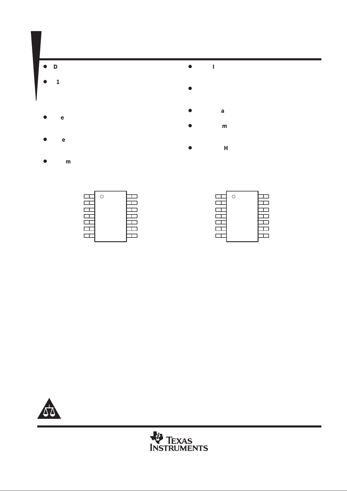
C
OSC
TACH
CP
V
PWR
V
OUT
NC
PGND
V
PWM
H+
H–
PHA
PHB
AGND
NC
THMC40 ...TACH OUTPUT
14-Pin SOP D Package
(TOP VIEW)
1
2
3
4
5
6
7
14
13
12
11
10
9
8
C
OSC
RD
CP
V
PWR
V
OUT
NC
PGND
V
PWM
H+
H–
PHA
PHB
AGND
NC
THMC41 . . . RD OUTPUT
14-Pin SOP D Package
(TOP VIEW)
description
The THMC40 and THMC41 are 2-phase, dc brushless motor (BLM) drive and control devices intended for use
with 12-Vdc cooling fans. Both devices include a high-efficiency PWM drive topology using integrated 0.5-Ω
(typical) LDMOS drivers, plus a speed control input stage to provide the industry’s first solution for efficient
speed control
inside
dc cooling fans. This patented solution eliminates the need for power drive components
on the main system board, thus reducing printed-circuit board (PCB) component count, PCB space, and
assembly time. This solution also offers other advantages over the two commonly used fan speed control
methods, adjustable external dc supply voltage, and adjustable external PWM drive duty cycle.
Unlike other methods which control speed external to the cooling fan, the THMC40 and THMC41 high-efficiency
PWM drive stage adjusts only the level of motor phase winding power. All other circuitry inside the fan obtains
power from the fixed dc voltage fan supply. This method eliminates the typical problem associated with an
external dc voltage regulation method causing loss of headroom to internal control circuitry at low fan supply
voltage and the resulting limitation of low-speed operation to ≈40%. The PWM drive method employed by the
THMC40 and THMC41 also reduces fan supply power consumption over the external linear regulation method,
which has V×I power loss due to the voltage drop across the regulator.
An external PWM drive method disrupts power to the motor and also to all internal fan circuitry . The THM40 and
THMC41 solution maintains all signal integrity with phase drive commutation and tachometer, while providing
reliable low speed fan operation down to 1 1% PWM. This method allows fan health monitoring over the full fan
speed range.
Copyright 2000, Texas Instruments Incorporated
PRODUCTION DATA information is current as of publication date.
Products conform to specifications per the terms of Texas Instruments
standard warranty. Production processing does not necessarily include
testing of all parameters.
Please be aware that an important notice concerning availability, standard warranty, and use in critical applications of
Texas Instruments semiconductor products and disclaimers thereto appears at the end of this data sheet.
THMC40, THMC41
VARIABLE SPEED 12-VDC BRUSHLESS FAN MOTOR DRIVERS
SLIS097 – MARCH 2000
2
POST OFFICE BOX 655303 • DALLAS, TEXAS 75265
description (continued)
The V
OUT
duty cycle, and thus the motor speed, is proportional to the voltage present at the V
PWM
input terminal.
This terminal allows controlling the fan speed via a DAC output from an external control IC or an RC-filtered
PWM output from a PC Super I/O chip.
The THMC40 and THMC41 have an internal Hall sensor amplifier and signal conditioner, global thermal
shutdown, locked rotor protection, and automatic restart after a locked rotor condition. The THMC40 provides
an open-drain tachometer output signal, while the THMC41 provides an open-drain locked rotor detection
output signal. These devices also provide a sleep-state mode to eliminate the need for an external power
component to disconnect the fan from the supply during a system sleep state or
instantly available
power down.
The THMC40 and THMC41 are primarily intended for cooling fan applications that require RPM speed control
and the availability of a tachometer or locked rotor detection signal.
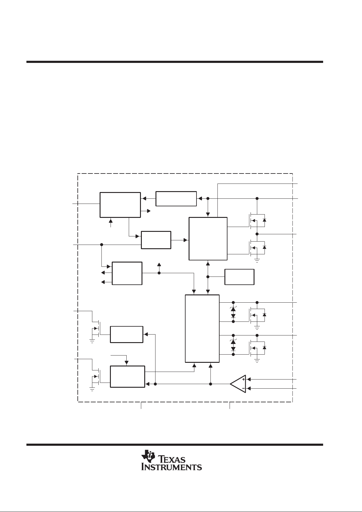
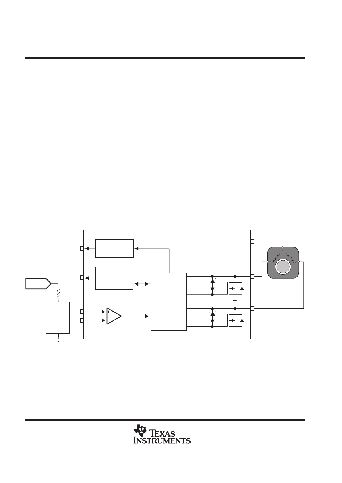
functional block diagram
Tachometer
Output
CP
V
PWM
Low-Side
Gate Drive
Control Logic
and Global
Thermal
Shutdown
High-Side Gate
Drive With
Synchronous
Rectification
Charge Pump
Locked Rotor
Detection and
Auto Restart
SLEEP
START and
SLEEP
Detection
PWM
Generator
PWM
Oscillator
23 kHz Nominal
PUC and V
REF
Thermal
Shutdown
OSC
V
START
V
SLEEP
OSC
PWM
SLEEP
C
OSC
TACH
(THMC40)
RD
(THMC41)
V
PWR
V
OUT
PHA
PHB
H+
H–
PGNDAGND
Hall Sensor
Comparator
THMC40, THMC41
VARIABLE SPEED 12-VDC BRUSHLESS FAN MOTOR DRIVERS
SLIS097 – MARCH 2000
3
POST OFFICE BOX 655303 • DALLAS, TEXAS 75265
Terminal Functions
TERMINAL
NAME NO.
I/O
DESCRIPTION
AGND 9 I IC analog ground and substrate connection
CP 3 I External charge pump capacitor
C
OSC
1 I/O External oscillator capacitor
H– 12 I Hall sensor negative input
H+ 13 I Hall sensor positive input
NC 6, 8 – No connection
PGND 7 I Power ground for high-side charge pump
PHA 11 O Low-side driver for phase A motor winding
PHB 10 O Low-side driver for phase B motor winding
RD 2 O Open-drain locked rotor detection output—THMC41 only
TACH 2 O Open-drain tachometer output signal—THMC40 only
V
OUT
5 O High-side PWM driver output for motor windings
V
PWR
4 I Supply voltage input
V
PWM
14 I PWM duty cycle control voltage input
absolute maximum ratings over operating case temperature range (unless otherwise noted)
†
(see Note 1)
Supply voltage input, V
PWR
18 V. . . . . . . . . . . . . . . . . . . . . . . . . . . . . . . . . . . . . . . . . . . . . . . . . . . . . . . . . . . . . . . . .
High-side driver, PWM output voltage, V
OUT
18 V. . . . . . . . . . . . . . . . . . . . . . . . . . . . . . . . . . . . . . . . . . . . . . . . . .
Low-side drivers, phase A and B output, V
PHA
, V
PHB
40 V. . . . . . . . . . . . . . . . . . . . . . . . . . . . . . . . . . . . . . . . . .
Hall sensor amplifier input voltage, V
H+
, VH– 7 V. . . . . . . . . . . . . . . . . . . . . . . . . . . . . . . . . . . . . . . . . . . . . . . . . . .
PWM duty cycle control input voltage, V
PWM
7 V. . . . . . . . . . . . . . . . . . . . . . . . . . . . . . . . . . . . . . . . . . . . . . . . . . .
Open-drain tachometer output voltage (THMC40), V
TACH
, or open-drain RD output voltage
(THMC41), VRD 7 V. . . . . . . . . . . . . . . . . . . . . . . . . . . . . . . . . . . . . . . . . . . . . . . . . . . . . . . . . . . . . . . . . . . . . . . . .
Oscillator capacitor voltage, V
COSC
7 V. . . . . . . . . . . . . . . . . . . . . . . . . . . . . . . . . . . . . . . . . . . . . . . . . . . . . . . . . . .
Charge pump capacitor voltage, VCP 30 V. . . . . . . . . . . . . . . . . . . . . . . . . . . . . . . . . . . . . . . . . . . . . . . . . . . . . . . . .
Continuous high-side PWM output source/sink current, I
OUT
1.5 A. . . . . . . . . . . . . . . . . . . . . . . . . . . . . . . . . . .
Continuous low-side PWM output sink current, I
PHA
, I
PHB
1.5 A. . . . . . . . . . . . . . . . . . . . . . . . . . . . . . . . . . . . .
Junction-to-case thermal resistance, R
θJC
26.9°C/W. . . . . . . . . . . . . . . . . . . . . . . . . . . . . . . . . . . . . . . . . . . . . . .
Junction-to-ambient thermal resistance , R
θJA
(see Note 2) 122.3°C/W. . . . . . . . . . . . . . . . . . . . . . . . . . . . . . .
Continuous power dissipation at 25°C , P
D
(see Note 3) 1022 mW. . . . . . . . . . . . . . . . . . . . . . . . . . . . . . . . . . .
Power derating factor above 25°C ambient , P
DERA TING
(see Note 4) 8.18 mW/°C. . . . . . . . . . . . . . . . . . . . .
Operating case temperature range, TC –30°C to 80°C. . . . . . . . . . . . . . . . . . . . . . . . . . . . . . . . . . . . . . . . . . . . . .
Storage temperature range, T
stg
–55°C to 150°C. . . . . . . . . . . . . . . . . . . . . . . . . . . . . . . . . . . . . . . . . . . . . . . . . . .
Maximum junction temperature, T
J
150°C. . . . . . . . . . . . . . . . . . . . . . . . . . . . . . . . . . . . . . . . . . . . . . . . . . . . . . . . .
Lead temperature (soldering, 10 sec), T
LEAD
300°C. . . . . . . . . . . . . . . . . . . . . . . . . . . . . . . . . . . . . . . . . . . . . . . .
†
Stresses beyond those listed under “absolute maximum ratings” may cause permanent damage to the device. These are stress ratings only, and
functional operation of the device at these or any other conditions beyond those indicated under “recommended operating conditions” is not
implied. Exposure to absolute-maximum-rated conditions for extended periods may affect device reliability.
NOTES: 1. All voltage values are with respect to GND.
2. JEDEC low-K board with 0 LFM airflow
3. 150°C maximum junction temperature, JEDEC low-K board with 0 LFM airflow
4. 80°C maximum ambient and 150°C maximum junction temperature
THMC40, THMC41
VARIABLE SPEED 12-VDC BRUSHLESS FAN MOTOR DRIVERS
SLIS097 – MARCH 2000
4
POST OFFICE BOX 655303 • DALLAS, TEXAS 75265
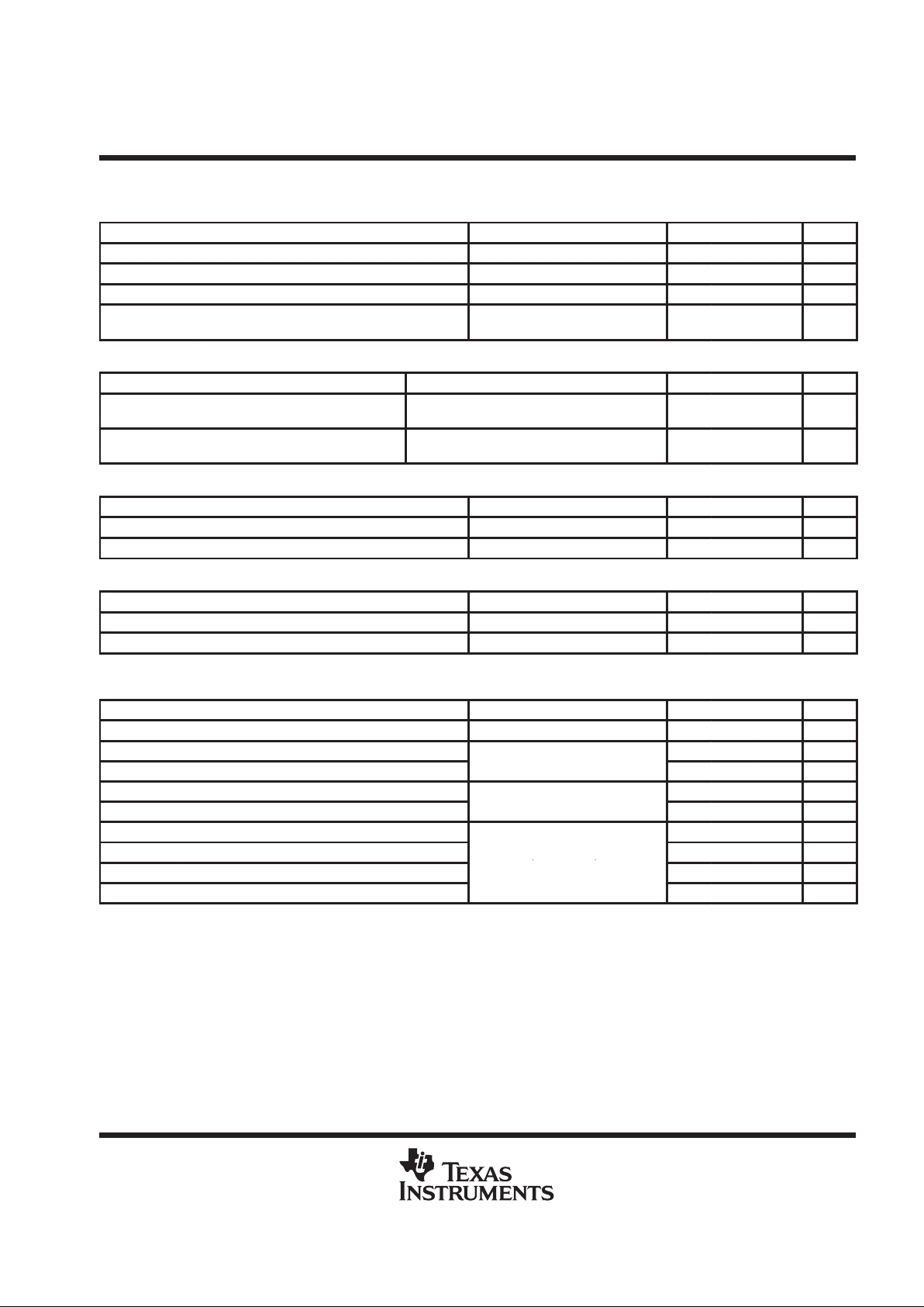
dc electrical characteristics, V
PWR
= 12 V, TA = – 30°C to 80°C (unless otherwise noted)
supply current
PARAMETER TEST CONDITIONS MIN TYP MAX UNITS
V
PWR
Supply voltage range 11 12 13 V
pp
Idle condition in locked rotor detect 2.5 5 mA
I
VPWR
V
PWR
su
pply current
I
LOAD
= –1 A, V
OUT
low, TA = 25°C 5 mA
I
SLEEP
Sleep-state current V
PWM
≤ 0.4 V 300 400 µA
PHA, PHB low-side phase winding driver outputs
PARAMETER TEST CONDITIONS MIN TYP MAX UNITS
I
LEAK
PHA,PHB output leakage current Output = OFF, V
PHx
= 12 V 0.1 10 µA
V
OL
PHA, PHB low-level output voltage Output = ON, I
PHx
= 1 A, TA = 25°C 0.5 0.6 V
R
DS(ON)
PHA, PHB output ON resistance Output = ON, I
PHx
= 1A, TA = 25°C 0.5 0.6 Ω
V
CLAMP
PHA, PHB output active clamp voltage Output = OFF, I
PHx
= 200 mA 32 38 V
Hall sensor signal conditioning
PARAMETER TEST CONDITIONS MIN TYP MAX UNITS
I
IB(HL)
Hall input bias current ±0.1 ±1 µA
V
ICR(HL)
ICR(HL) common-mode input voltage range 1 3.5 V
V
IO
Hall comparator input offset voltage Over V
ICR(HL)
= 1 V to 3.5 V –7 0 7 mV
V
OUT
high-side phase winding driver output
PARAMETER TEST CONDITIONS MIN TYP MAX UNITS
I
LEAK
V
OUT
output sleep-state leakage current
Sleep state engaged,
V
VOUT
= 0 V to V
PWR
±0.1 ±10 µA
V
OH
V
OUT
high-level output voltage
Run state, Output high
I
= –1 A, T
= 25°C
V
PWR
– 0.4
V
PWR
– 0.6
V
R
DS(ON)
V
OUT
output high-side resistance to V
PWR
VOUT
,
A
0.4 0.6 Ω
V
RECIR
V
OUT
output recirculation voltage
Run state, Output low
– 0.3 – 0.5 V
R
DS(ON)(SYNC)VOUT
synchronous switch resistance to PGND
,
I
VOUT
= –1 A, TA = 25°C
0.3 0.5 Ω
I
LIMIT
Pulsed V
OUT
synchronous rectification current
limit
Run state, V
OUT=VPWR
=12V,
V
COSC
> V
PWM,
t
PULSE
= 100 µs, See Note 5
2 2.6 A
CP high-side gate drive charge pump capacitor input
PARAMETER TEST CONDITIONS MIN TYP MAX UNITS
V
CP
Charge pump voltage I
VCP
= –60 µA, V
PWM
= 2.5 V 22 26 V
V
CP(UVLO)VCP
undervoltage lock-out 6.5 7.6 8.5 V
C
OSC
external oscillator capacitor
PARAMETER TEST CONDITIONS MIN TYP MAX UNITS
I
CHARGE
C
OSC
charge source current V
COSC
= 1.4 V, Charge mode –130 –180 –230 µA
I
DISCHARGECOSC
discharge sink current V
COSC
= 1.4 V, Discharge mode 130 180 230 µA
V
DISCHARGECOSC
upper threshold for switching to current sink 2 2.3 2.6 V
V
CHARGE
C
OSC
lower threshold for switching to current
source
0.43 0.5 0.57 V
NOTE 5: V
OUT
current limit, in conjunction with thermal shutdown function, provides device survivability under V
OUT
-to-V
PWR
short condition.
THMC40, THMC41
VARIABLE SPEED 12-VDC BRUSHLESS FAN MOTOR DRIVERS
SLIS097 – MARCH 2000
5
POST OFFICE BOX 655303 • DALLAS, TEXAS 75265
dc electrical characteristics, V
PWR
= 12 V , TA = –30°C to 80°C (unless otherwise noted) (continued)
V
PWM
high-side PWM duty cycle adjust input
PARAMETER TEST CONDITIONS MIN TYP MAX UNITS
I
IB(PWM)
V
PWM
input bias current V
PWM
= 0 V to 3 V ±1 µA
V
PWM
(100%) V
PWM
voltage equivalent to 100% duty cycle 2.3 V
V
SLEEP
V
PWM
voltage threshold to engage sleep mode 0.6 0.7 V
V
START
V
PWM
voltage threshold to disengage sleep
mode
0.8 0.9 V
thermal shutdown characteristics
PARAMETER TEST CONDITIONS MIN TYP MAX UNITS
T
TSD
V
OUT
, PHA, PHB global thermal shutdown
thresholds
Temperature increasing until outputs are off,
See Note 6
150 185 °C
T
HYST
Thermal shutdown hysteresis
After T
TSD
, temperature decreasing until out-
puts return to normal operation, See Note 6
15 °C
TACH Tachometer open-drain output (THMC40)
PARAMETER TEST CONDITIONS MIN TYP MAX UNITS
I
TACHLEAK
TACH high-level output leakage current V
TACH
= 5 V 0.1 1 µA
V
OL
TACH low-level output voltage I
TACH
= 5 mA 0.1 0.3 V
RD locked rotor detection open-drain output (THMC41)
PARAMETER TEST CONDITIONS MIN TYP MAX UNITS
I
RDLEAK
RD high-level output leakage current VRD = 5 V, Locked rotor condition 0.1 1 µA
V
OL
RD low-level output voltage IRD = 5 mA, No locked rotor 0.1 0.3 V
ac electrical characteristics, V
PWR
= 12 V, TA = –30°C to 80°C (unless otherwise noted)
PARAMETER TEST CONDITIONS MIN TYP MAX UNITS
f
PWM
High-side gate drive PWM frequency C
OSC
= 2200 pF 22.7 kHz
t
RD
Locked rotor detect delay time
p
1 s
t
RETRY
Auto-restart delay time
C
OSC
=
2200 pF, See Figure 9
8 s
t
HALL
Hall zero-crossing deglitch time
25 µs
t
DEAD(PHx)
Dead time between phase commutations
See Figure 2
5 µs
t
f(OUT)
V
OUT
output fall time 25 ns
t
r(OUT)
V
OUT
output rise time
R
= 20 Ω , L
= 5 mH,
25 ns
t
f(PHx)
PHA or PHB fall time
L
,
L
,
See Note 6
1 µs
t
r(PHx)
PHA or PHB rise time 1 µs
NOTE 6: Design targets only. Not tested in production.
THMC40, THMC41
VARIABLE SPEED 12-VDC BRUSHLESS FAN MOTOR DRIVERS
SLIS097 – MARCH 2000
6
POST OFFICE BOX 655303 • DALLAS, TEXAS 75265
PRINCIPLES OF OPERATION
general overview
The THMC40 and THMC41 are 2-phase dc brushless fan motor drivers with PWM speed control intended
primarily for applications requiring a wide speed control range and an open-drain tachometer output signal
(THMC40), or a locked rotor detection output (THMC41). The V
OUT
drive duty cycle, and thus fan speed, is
proportional to the voltage level at the V
PWM
input terminal. Each device has an internal Hall sensor
comparator/signal conditioner, a low power sleep-state mode, locked rotor protection with automatic restart
after a locked rotor condition, and over-temperature protection. The tachometer signal (THMC40) can be used
to monitor the
health
of the fan or to close an external loop based on fan RPM. The THMC40 and THMC41
provide a more efficient drive solution to fan RPM control than external linear voltage control. This solution is
also considerably more efficient than controlling dc brushless fan RPM using external PWM drive.
low-side motor phase winding driver outputs (PHA, PHB)
The PHA and PHB outputs provide low-side drive of the motor’s two stator phase windings (see block diagram
and Figure 1). These outputs have a typical R
DS(ON)
of 400 mΩ at 25°C and a 1-A continuous current rating.
The PHA and PHB outputs have an active flyback clamp (V
ZCLAMP
in Figure 1) of 38 V (typical) to snub inductive
energy when a phase drive switches off. The outputs also have global thermal shutdown to prevent device
failure.
Drive commutation of PHA and PHB outputs is controlled according to rotor position monitored by a Hall-effect
position sensor. Discussion of this function is found in the following section, and the relationship between PHA
and PHB outputs to Hall input signal is shown in Figure 2.
Locked Rotor
Detection and
Auto-Restart
V
OUT
TACH
(THMC40)
NS
SN
Tachometer
Output Driver
V
ZCLAMP
V
ZCLAMP
Low-Side
Gate Drive
Control
Logic, and
Global
Thermal
Shutdown
Naked
Hall
Sensor
V
PWR
Hall Sensor
Comparator
RD
(THMC41)
H+
H–
PHA
PHB
Figure 1. Low-Side Gate Drive Block Diagram

THMC40, THMC41
VARIABLE SPEED 12-VDC BRUSHLESS FAN MOTOR DRIVERS
SLIS097 – MARCH 2000
7
POST OFFICE BOX 655303 • DALLAS, TEXAS 75265
Hall sensor comparator and signal conditioning inputs (H+, H–)
Referring to Figure 1, the THMC40 and THMC41 have an internal Hall sensor comparator allowing the use of
low-cost naked Hall sense elements. The Hall signal conditioning block receives a low-level differential voltage
from the naked Hall position sensor element. The comparator then implements a zero differential voltage
crossing detection with a deglitch time of 25 µs (typical) to reject noise on the Hall signal inputs. Referring to
Figure 2, the PHx drive that was on (low) turns off after the 25-µs deglitch time is reached. Then the opposite
PHx drive turns on after another delay time. This 5-µs (typical)
dead time
is implemented to prevent both phases
from conducting simultaneously and to allow time for the inductive energy to be snubbed from the phase that
was just turned off. The Hall comparator circuit has an input offset voltage (V
IO
) which is not greater than ±7
mV. The common-mode input voltage range is 1 V to 3.5 V (see Figure 2).
t
DEAD(PHx)
V
CM
PHA Output
Voltage
PHB Output
Voltage
OFF
ON
OFF
ON
V
IO
5 µst
HALL
25 µs
t
DEAD(PHx)
t
HALL
25 µs
5 µs
Time
TACH Output
Voltage (THMC40)
OFF
ON
Hall Sensor
Waveform
(VH+ - VH–)
Figure 2. Hall Sensor Signal Conditioning Waveforms
Table 1 shows PHA and PHB commutation, and TACH output (THMC40) functionality:
Table 1. PHA and PHB Low-Side Drive Commutation and TACH Functionality
H+ H– PHA PHB
TACH
(THMC40)
+ – High (OFF) Low (ON) High (OFF)
– + Low (ON) High (OFF) Low (ON)

THMC40, THMC41
VARIABLE SPEED 12-VDC BRUSHLESS FAN MOTOR DRIVERS
SLIS097 – MARCH 2000
8
POST OFFICE BOX 655303 • DALLAS, TEXAS 75265
high-side PWM output driver (V
OUT
)
Referring to Figure 3, V
OUT
is a drive output to provide PWM controlled power to the common node of the motor
phase windings using an internally generated PWM signal. The PWM duty cycle controls the effective drive
power to the motor, and thus motor speed. The high-side V
OUT
DMOS output transistor has a typical R
DS(ON)
of 400 mΩ at 25°C and a 1-A continuous current.
PWM
CP
C
OSC
Charge Pump,
HS Gate Drive,
Synchronous
Rectification,
and
Global Thermal
Shutdown
Triangle W ave
Generator
0.5 V to 2.3 V
PUC
Synchronous
Low-Side
Switch
High-Side
Driver
0.1 µF
V
PWR
V
OUT
V
PWM
2200 pF
COMP
Figure 3. High-Side PWM Drive
The frequency of the PWM drive (typically 23 kHz) is such that the L/R time constant of the motor phase winding
filters the current. Referring to Figure 4, during the on-time (t
ON
) of a PWM period, V
OUT
is driven high forcing
voltage across a phase winding and increasing the current. During t
OFF,
PWM off-time, the V
OUT
high-side
DMOS is switched off, the phase winding inductive energy is recirculated, and the current decreases. To
minimize the voltage drop and the resulting energy loss during recirculation, a low-side DMOS synchronous
switch is provided, as shown in Figure 3. This low-side DMOS device has a 2-A minimum current limit to prevent
device failures should a solder bridge occur between the adjacent V
PWR
and V
OUT
terminals.
I
RECIRCULATE
I
MOTOR
t
ON
t
OFF
I
DRIVE
t
PWM
PWM
Time
Figure 4. Motor Current Waveform
The V
OUT
circuit is protected by the global thermal shutdown of the THMC40 and THMC41 by turning off both
the high-side and low-side DMOS drivers when an over-temperature condition is detected. V
OUT
is also held
off when the charge-pump voltage (V
CP
) is lower than its undervoltage lock-out threshold, V
CP(UVLO)
.

THMC40, THMC41
VARIABLE SPEED 12-VDC BRUSHLESS FAN MOTOR DRIVERS
SLIS097 – MARCH 2000
9
POST OFFICE BOX 655303 • DALLAS, TEXAS 75265
charge pump (CP)
THMC40 and THMC41 have an internal charge pump which utilizes an external reservoir capacitor (CP) to
generate the gate-drive voltage for the V
OUT
output high-side DMOS transistor (see Figure 3). The
recommended value for CP is 0.1 µF, with a minimum rating of 35 WVdc. The charge pump is disabled during
the sleep state (see the sleep/run state section) to minimize current consumption into V
PWR
. The charge pump
also incorporates internal undervoltage lockout detection used to disable V
OUT
when the charge pump voltage
does not have an adequate level above V
PWR
to fully drive the high-side DMOS gate. Thus, the VCP (UVLO),
in conjunction with the charge pump start-up time, delays the V
OUT
drive for a short time after the device has
transitioned from sleep to run state, until the charge pump voltage reaches the UVLO threshold.
PWM oscillator/triangle waveform generator (C
OSC
)
The PWM oscillator uses source and sink currents switched into an external capacitor (C
OSC
) to set the PWM
frequency and generate a triangle waveform. A PWM oscillator cycle consists of charging C
OSC
with a constant
current source (–180 µA typical) until the C
OSC
voltage ramps up to an upper threshold (2.3 V typical), and then
discharging C
OSC
with a constant current sink (180 µA typical) until the C
OSC
voltage ramps down to a lower
threshold (0.5 V typical). The charge/discharge cycle is repeated each time the 2.3-V or 0.5-V threshold is
reached (see Figure 5).
V
2.3 V
S
R
Q
Q
V
REF
V
PWR
C
OSC
V
PWM
2200 pF
PWM
–180 µA
2.3 V
0.5 V
180 µA
Time
0.5 V
0
Q
Q
V
COSC
Figure 5. PWM Triangle Waveform Generator
The following equation can be used to calculate the value of C
OSC
needed for a desired PWM frequency , f
PWM
:
C
OSC(max)
+
I
CHARGE(min)
2 f
PWM(min)
ǒV
DISCHARGE
*
V
CHARGE
Ǔ

THMC40, THMC41
VARIABLE SPEED 12-VDC BRUSHLESS FAN MOTOR DRIVERS
SLIS097 – MARCH 2000
10
POST OFFICE BOX 655303 • DALLAS, TEXAS 75265
PWM duty cycle control voltage (V
PWM
) – dc control voltage input
The voltage at the V
PWM
terminal determines the PWM duty cycle of the output (V
OUT
) to control drive power
to the fan motor, and thus control fan speed (see Figures 3 and 6). The V
PWM
voltage is internally compared
against the 0.5-V to 2.3-V triangle waveform generated on the C
OSC
terminal. The PWM signal output from this
comparator has a duty cycle proportional to the voltage at V
PWM
, as shown in Figure 6. The output of this
comparator is used as the PWM input to the V
OUT
drive stage.
50
40
20
10
0
90
30
0 0.2 0.4 0.6 0.8 1 1.2
70
60
80
100
1.4 1.6 1.8 2.4
– Duty Cycle – %
V
OUT
2 2.2
V
PWM
– Input Voltage – V
RUN STATE
SLEEP
STATE
V
SLEEP
=0.7 V
V
START
= 0.8 V
Must be exceeded
to enter run state
V
OUT
Duty Cycle =
(V
PWM
- 0.5)/1.8 × 100
Figure 6. Relationship of V
OUT
Duty Cycle, V
START
, and V
SLEEP
vs V
PWM
Input Voltage
PWM duty cycle control voltage (V
PWM
) – digital PWM control input
To allow control of the THMC40 and THMC41 by either a PWM or a dc input control signal, it is recommended
that the fan manufacturer includes a 100-kΩ, 0.1-µF RC filter between the speed control wire and the V
PWM
terminal (see Figure 7). This method allows the end user to control the fan speed with either a PWM signal or
a dc control voltage. Many PC Super I/O ICs and hardware monitoring ICs provide one of the two fan speed
control outputs. Therefore, fans with THMC40 and THMC41 ICs can be used with a wide variety of control
schemes to provide variable fan speed without an external fan drive power stage.
C = 0.1 µF
V
PWM
PWM Generator
(Super I/O or
HW Monitor)
PC Motherboard
Inside Cooling Fan
R = 100 kΩ
THMC40
and
THMC41
Full Speed Option
V
FAN
Speed
Control
1 – 10 MΩ†
1 – 10 MΩ
†
Sleep State Option
†
Optional resistors control fan operation with open speed control input.
Figure 7. PWM Input Control With RC Filter Inside the Cooling Fan

THMC40, THMC41
VARIABLE SPEED 12-VDC BRUSHLESS FAN MOTOR DRIVERS
SLIS097 – MARCH 2000
11
POST OFFICE BOX 655303 • DALLAS, TEXAS 75265
PWM duty cycle control voltage (V
PWM
) – digital PWM control input (continued)
Figure 8 illustrates the relationship between V
OUT
output duty-cycle and a 0–3.3-V digital PWM input control
signal.
– Duty Cycle – %
V
OUT
3.3-V Duty Cycle Input to RC Filter
50
40
20
10
0
90
30
0102030405060
70
60
80
100
70 80 90 100
RUN STATE
SLEEP
STATE
V
OUT
% =((3.3 V ×
(Input%÷100)-0.5)÷1.8) ×100
V
SLEEP=21%
V
START
= 24%
Must be exceeded to
enter run state
Figure 8. Relationship of V
OUT
Duty Cycle, V
SLEEP
, V
ST ART
vs 0–3.3 V PWM Input Duty Cycle
sleep/run state
Sleep-state and run-state modes are provided, as illustrated in Figures 6 and 8. The sleep state is intended to
minimize V
PWR
(fan) supply current requirements (300 µA typical) when cooling fan operation is not required.
This feature is especially beneficial for PC OEMs needing to meet the
instantly available
PC requirements
without the use of additional external circuitry.
The sleep state is engaged when the V
PWM
input voltage is below the V
SLEEP
threshold (0.7 V typical, 1 1.1%
duty cycle). During the sleep state, all output drivers are turned off and any unused circuits are powered down
to minimize current drain. Once sleep state is engaged, V
PWM
must exceed the V
ST ART
threshold (0.8 V typical,
17% duty cycle) to disable the sleep state and enter the run state, allowing the motor to be driven. Once the
run state is engaged, outputs V
OUT
, PHA, and PHB are active and the V
PWM
voltage can be decreased to obtain
minimum fan speed down to the V
SLEEP
threshold. This procedure allows the user to overcome initial motor
stiction with a PWM duty cycle of 17% to avoid the possibility of false locked rotor detection during initial start-up.
See Figure 6 for the V
PWM
input voltage relationship to sleep mode and V
OUT
duty cycle.
A control device with a voltage range of 0 V to 2.5 V is recommended to provide the adjustable V
PWM
reference
voltage to the THMC40 and THMC41. A 2.5-V DAC is an optimal choice as the controlling circuitry , whether as
a stand-alone device, or as an integrated function in a multiple-function device. Using a control device without
a minimum 0.5-V to 2.3-V range reduces the RPM control range of the fan motor and may not allow duty-cycle
settings of 0% and/or 100%.
thermal shutdown
The THMC40 and THMC41 provide protection against excessive device temperature with a thermal sensor that
monitors the die temperature. Should some operating or abnormal condition cause the die temperature to
exceed T
TSD
, the thermal shutdown threshold (165°C typical), all output drivers are turned off. Once T
TSD
has
been exceeded, the die temperature must fall below a hysteresis temperature (typical T
TSD
–15°C) before the
output drivers are re-enabled.

THMC40, THMC41
VARIABLE SPEED 12-VDC BRUSHLESS FAN MOTOR DRIVERS
SLIS097 – MARCH 2000
12
POST OFFICE BOX 655303 • DALLAS, TEXAS 75265
locked rotor protection
An internal digital timer monitors the output of the Hall sensor amplifier. When a change in commutation state
is not observed within one second (typical with 2200 pF C
OSC
), the V
OUT
, PHA, and PHB outputs are disabled
for eight seconds (typical with 2200 pF C
OSC
). After the outputs have been disabled for eight seconds (typical
with 2200 pF C
OSC
), the THMC40 and THMC41 re-enable the V
OUT
, PHA, and PHB outputs to automatically
restart the motor after a locked rotor condition. If the locked rotor condition still exists, the above process repeats
itself until the condition is removed, or the THMC40 and THMC41 are powered down (see Figure 9).
NOTE:
The locked rotor detection time and auto-retry time are proportional to the PWM frequency, and
therefore to the value of C
OSC
. With a C
OSC
value of 2200 pF, the PWM frequency is typically
22.7 kHz, locked rotor detection time is typically one second, and auto-retry time is typically
eight seconds.
1s
Hall Sensor
Comparator
Output
1s 8s8s
V
OUT
, PHA and
PHB Output
Enable
RD Output
(THMC41)
Tach Output
(THMC40)
Figure 9. Typical Locked Rotor Protection Timing Waveforms

THMC40, THMC41
VARIABLE SPEED 12-VDC BRUSHLESS FAN MOTOR DRIVERS
SLIS097 – MARCH 2000
13
POST OFFICE BOX 655303 • DALLAS, TEXAS 75265
open-drain tachometer output (TACH)—THMC40 Only
The THMC40 T ACH output is an open-drain output activated by the Hall sensor comparator output (see Figure
9). When the Hall sensor comparator output is high, the T ACH output floats high. When the Hall sensor amplifier
output is low, the TACH output is pulled low. The resulting output signal has two pulses per revolution on a
four-pole motor.
The T ACH output can be used to monitor and measure actual fan speed. This output can also be used as part
of a closed-loop speed control system.
NOTE:
It is recommended that the fan manufacturer not place a pullup resistor for this terminal on the fan
circuit board. Leaving the output as open-drain allows the end user to pull up this terminal with an
external resistor to the supply voltage of their choice (that is, 3.3 V or 5 V).
open-drain locked rotor detection output—THMC41 only
The THMC41 RD output is an open-drain output pulled low during normal fan operation and allowed to float
during a locked rotor condition (see Figure 9). This signal can be used to alert the system of a locked rotor
condition.
The RD output can also be used as a
fan present
or
fan OK
signal by using a general-purpose input terminal
on a PC Super I/O chip to detect the logic state of this terminal. When this input is high, the signal indicates that
the fan has been disconnected or is in a locked rotor condition.
NOTE:
It is recommended that the fan manufacturer not place a pullup resistor for this terminal on the fan
circuit board. Leaving the output as open-drain allows the end user to pull up this terminal with an
external resistor to the supply voltage of their choice (that is, 3.3V or 5V).
supply voltage input (V
PWR
)
The V
PWR
terminal serves as the voltage supply input to the THMC40 and THMC41. A 0.1-µF bypass capacitor
should be placed as close to this terminal as the layout permits. Additional bulk capacitance of 2.2 µF to 10 µF
on this terminal is highly recommended to reduce current spikes on the supply line during motor commutation,
thus reducing radiated emissions from the fan. See Application Information for further details.

THMC40, THMC41
VARIABLE SPEED 12-VDC BRUSHLESS FAN MOTOR DRIVERS
SLIS097 – MARCH 2000
14
POST OFFICE BOX 655303 • DALLAS, TEXAS 75265
APPLICATION INFORMATION
C
OSC
TACH
CP
V
PWR
V
OUT
NC
PGND
V
PWM
H+
H–
PHA
PHB
AGND
NC
THMC40D
MOTOR
LO
R1
100 kΩ
L2
L1
HALL
SENSOR
1
2
3
4
5
6
7
14
12
13
11
10
9
8
0.1 µF
C5
10 µF
16 V
GND
Speed Control Input
2200 pF
24
3
1
0.1 µF
TACH
+12 V
CR1
1N4002
R2
3.01 kΩ
C4
0.1 µF
NOTE: Traces in bold handle highest current.
+
C3
C2
C1
Full Speed Option
Sleep State Option
†
Optional resistors control fan operation with open speed control input.
1 – 10 MΩ†
1 – 10 MΩ†
‡
‡
An analog ground trace should be connected close to the ground connection of C4 and C5.
Figure 10. THMC40 Application Schematic

THMC40, THMC41
VARIABLE SPEED 12-VDC BRUSHLESS FAN MOTOR DRIVERS
SLIS097 – MARCH 2000
15
POST OFFICE BOX 655303 • DALLAS, TEXAS 75265
APPLICATION INFORMATION
C
OSC
RD
CP
V
PWR
V
OUT
NC
PGND
V
PWM
H+
H–
PHA
PHB
AGND
NC
THMC41D
MOTOR
LO
R1
100 kΩ
L2
L1
HALL
SENSOR
1
2
3
4
5
6
7
14
12
13
11
10
9
8
0.1 µF
C5
10 µF
16 V
GND
2200 pF
24
3
1
0.1 µF
RD+12 V
CR1
1N4002
R2
3.01 kΩ
C4
0.1 µF
+
C3
C2
C1
Speed Control Input
Full Speed Option
Sleep State Option
1 – 10 MΩ†
1 – 10 MΩ†
NOTE: Traces in bold handle highest current.
†
Optional resistors control fan operation with open speed control input.
‡
‡
An analog ground trace should be connected close to the ground connection of C4 and C5.
Figure 11. THMC41 Application Schematic

THMC40, THMC41
VARIABLE SPEED 12-VDC BRUSHLESS FAN MOTOR DRIVERS
SLIS097 – MARCH 2000
16
POST OFFICE BOX 655303 • DALLAS, TEXAS 75265
MECHANICAL DATA
D (R-PDSO-G**) PLASTIC SMALL-OUTLINE PACKAGE
14 PINS SHOWN
4040047/D 10/96
0.228 (5,80)
0.244 (6,20)
0.069 (1,75) MAX
0.010 (0,25)
0.004 (0,10)
1
14
0.014 (0,35)
0.020 (0,51)
A
0.157 (4,00)
0.150 (3,81)
7
8
0.044 (1,12)
0.016 (0,40)
Seating Plane
0.010 (0,25)
PINS **
0.008 (0,20) NOM
A MIN
A MAX
DIM
Gage Plane
0.189
(4,80)
(5,00)
0.197
8
(8,55)
(8,75)
0.337
14
0.344
(9,80)
16
0.394
(10,00)
0.386
0.004 (0,10)
M
0.010 (0,25)
0.050 (1,27)
0°–8°
NOTES: A. All linear dimensions are in inches (millimeters).
B. This drawing is subject to change without notice.
C. Body dimensions do not include mold flash or protrusion, not to exceed 0.006 (0,15).
D. Falls within JEDEC MS-012

IMPORTANT NOTICE
T exas Instruments and its subsidiaries (TI) reserve the right to make changes to their products or to discontinue
any product or service without notice, and advise customers to obtain the latest version of relevant information
to verify, before placing orders, that information being relied on is current and complete. All products are sold
subject to the terms and conditions of sale supplied at the time of order acknowledgment, including those
pertaining to warranty, patent infringement, and limitation of liability.
TI warrants performance of its semiconductor products to the specifications applicable at the time of sale in
accordance with TI’s standard warranty. Testing and other quality control techniques are utilized to the extent
TI deems necessary to support this warranty. Specific testing of all parameters of each device is not necessarily
performed, except those mandated by government requirements.
Customers are responsible for their applications using TI components.
In order to minimize risks associated with the customer’s applications, adequate design and operating
safeguards must be provided by the customer to minimize inherent or procedural hazards.
TI assumes no liability for applications assistance or customer product design. TI does not warrant or represent
that any license, either express or implied, is granted under any patent right, copyright, mask work right, or other
intellectual property right of TI covering or relating to any combination, machine, or process in which such
semiconductor products or services might be or are used. TI’s publication of information regarding any third
party’s products or services does not constitute TI’s approval, warranty or endorsement thereof.
Copyright 2000, Texas Instruments Incorporated
 Loading...