

THMC10
REMOTE/LOCAL TEMPERATURE MONITOR
WITH SMBus INTERFACE
SLIS089 – DECEMBER 1999
1
POST OFFICE BOX 655303 • DALLAS, TEXAS 75265
D
T wo-Wire SMBus Serial Interface
D
On-Chip and External Diode-Connected
Transistor Temperature Monitoring
– ±2.5°C Accuracy for On-Die
– ±3°C Accuracy for External
D
Programmable Under/Overtemperature
Limits
D
Under/Overtemperature Interrupt Signal to
Host Controller
D
Low Operating Current ...35 µA (Average)
D
Low Standby Current ...3 µA
D
3-V to 3.6-V Supply Voltage Range
description
The THMC10 is a dual digital temperature monitor with under/overtemperature alerts intended for use in
personal computer systems or any other system requiring local as well as remote temperature monitoring and
management (e.g., servers and workstations). The device may be used in smart battery applications and
memory modules. The device is designed to measure the temperature on a microprocessor using a
diode-connected transistor on the microprocessor die, such as the one present on the Intel
Pentium II, III,
and the Sun UltraSP ARC. The device may also be used with a low-cost, diode-connected, discrete transistor,
such as a 2N3904 or 2N3906, for remote temperature sensing applications.
The THMC10 uses a two-current measurement technique on a single diode-connected transistor that cancels
the absolute value of the remote transistor’s VBE; therefore, no calibration is needed. The second channel
measures an on-chip temperature sensor which can be used to monitor the ambient temperature in the
THMC10’s operating environment.
The THMC10 uses a two-wire, SMBus interface to report temperature in an 8-bit, 2s complement format in °C.
Under/overtemperature limits for both the on-chip and remote temperature sensors are user programmable via
the SMBus interface. The ALERT
terminal can be used as an interrupt or SMBus alert function to indicate
under/overtemperature. The STBY terminal and the
start/stop
bit in the SMBus interface allow the device to
enter a low current standby mode (typically <10 µA).
The THMC10 also provides diagnostics via the ALERT terminal and the SMBus interface for an open remote
sensor connection or if the sensor connection is shorted to V
DD.
Copyright 1999, Texas Instruments Incorporated
PRODUCTION DATA information is current as of publication date.
Products conform to specifications per the terms of Texas Instruments
standard warranty. Production processing does not necessarily include
testing of all parameters.
Please be aware that an important notice concerning availability, standard warranty, and use in critical applications of
Texas Instruments semiconductor products and disclaimers thereto appears at the end of this data sheet.
Intel and Pentium are registered trademarks of Intel Corporation.
Sun is a registered trademark and UltraSPARC is a trademark of Sun Microsystems.
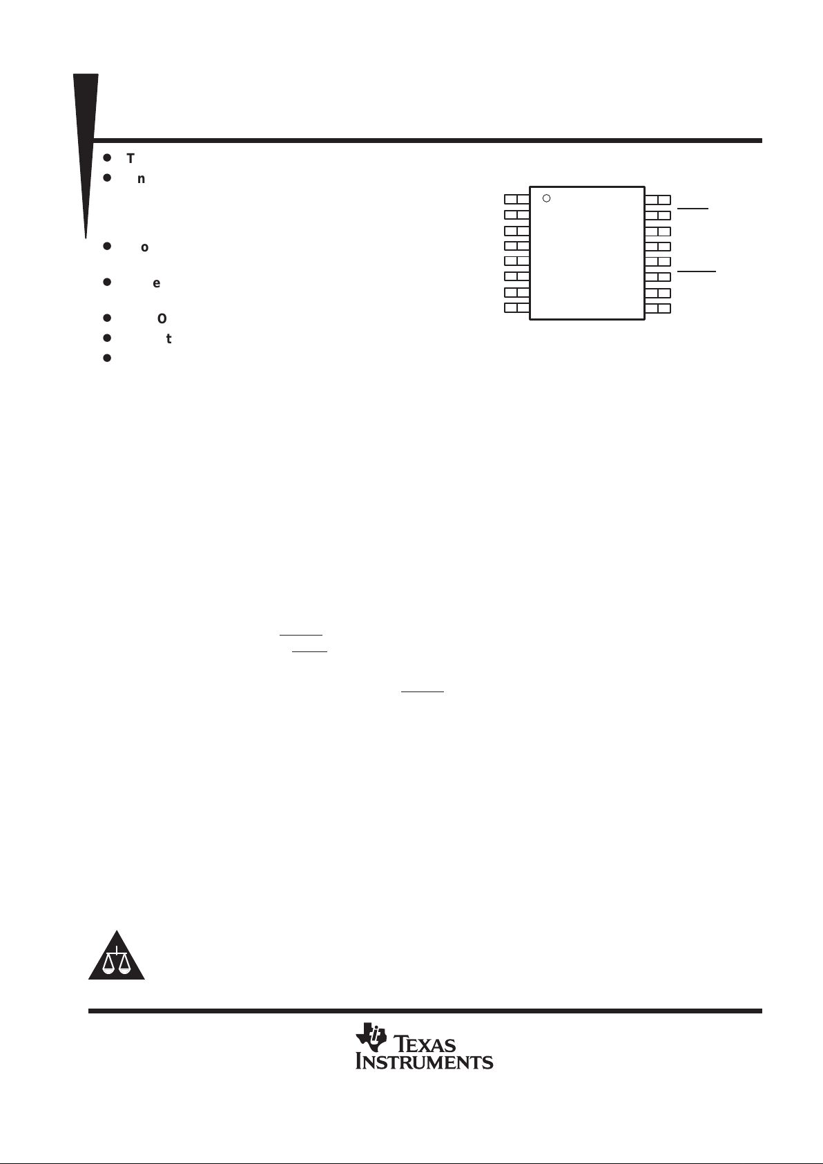
1
2
3
4
5
6
7
8
16
15
14
13
12
11
10
9
N/C
V
DD
DXP
DXN
N/C
ADD1
GND
GND
N/C
STBY
SCLK
N/C
SDATA
ALERT
ADD0
N/C
SSOP DBQ Package
(TOP VIEW)
THMC10
THMC10
REMOTE/LOCAL TEMPERATURE MONITOR
WITH SMBus INTERFACE
SLIS089 – DECEMBER 1999
2
POST OFFICE BOX 655303 • DALLAS, TEXAS 75265
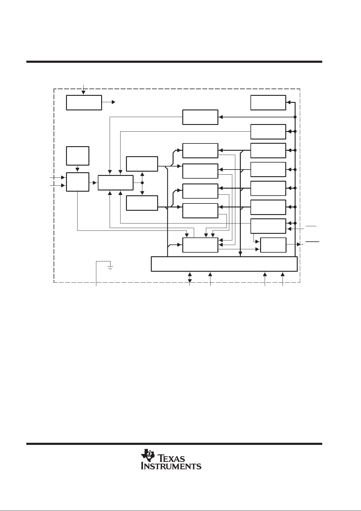
schematic/block diagram
Interrupt
Masking
GND
STBY
DXP
Configuration
Register
High Limit
Register
Low Limit
Register
High Limit
Register
Low Limit
Register
Auto-Acquire
Rate Register
ADDR Pointer
Register
One-Shot
Register
Low Limit
Comparator
High Limit
Comparator
Status
Register
8-Bit A/D
Converter
Power-up
Clear
On-Chip
Temp
Sensor
Analog
MUX
Local Temp
Register
Remote Temp
Register
Low Limit
Comparator
High Limit
Comparator
SDATA
SMBus Interface
DXN
ALERT
V
DD
To All Registers
SCLK ADD0 ADD1
THMC10
REMOTE/LOCAL TEMPERATURE MONITOR
WITH SMBus INTERFACE
SLIS089 – DECEMBER 1999
3
POST OFFICE BOX 655303 • DALLAS, TEXAS 75265
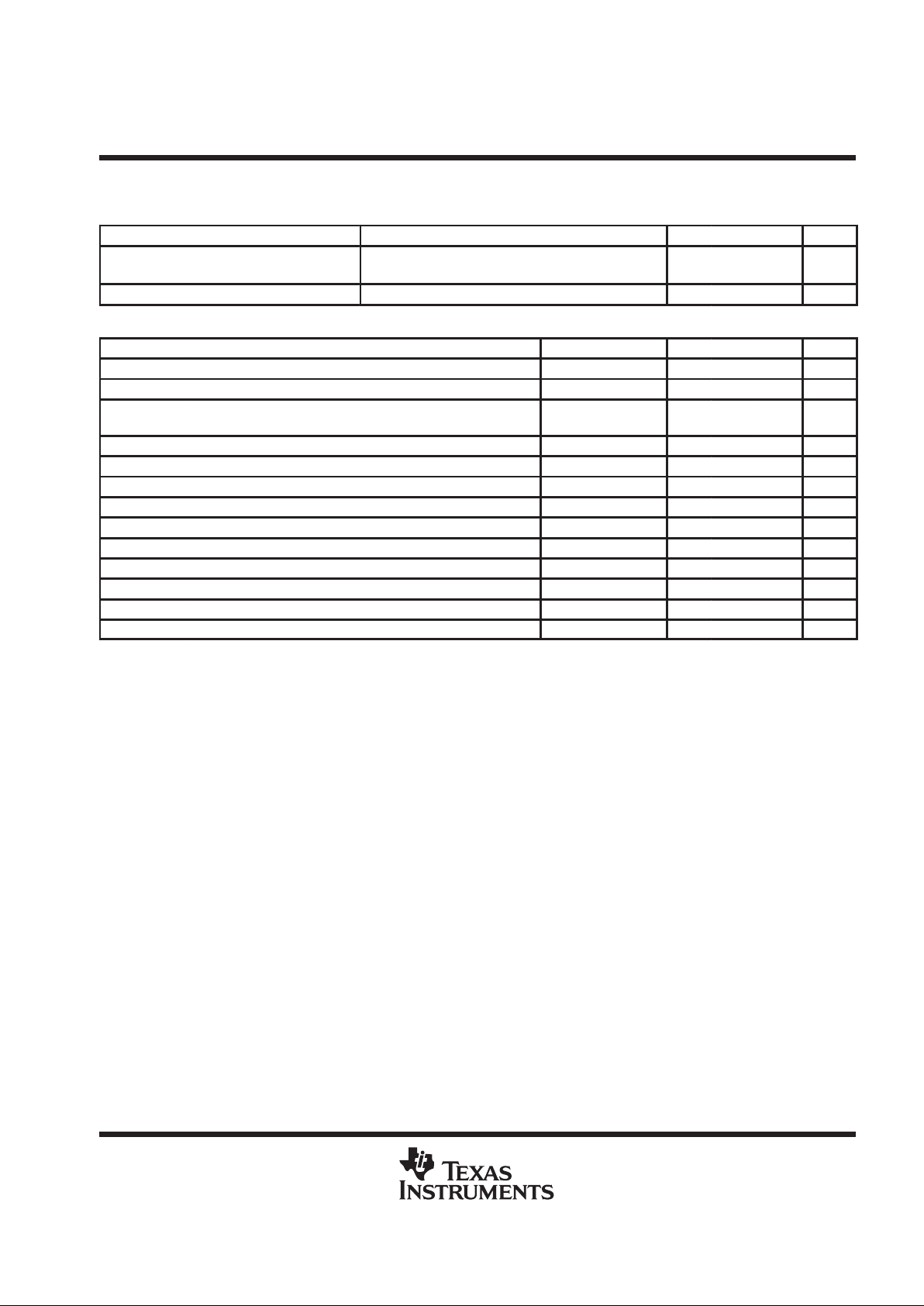
Terminal Functions
TERMINAL
NAME NO.
I/O
DESCRIPTION
ADD0 10 I SMBus address select terminal 0 (Note: Excess capacitance on this terminal may cause SMBus address
recognition problems.)
ADD1 6 I SMBus address select terminal 1 (Note: Excess capacitance on this terminal may cause SMBus address
recognition problems.)
ALERT 11 O Active low temperature interrupt signal
DXN 4 I/O Current sink for external diode connected transistor and A/D negative input (Do not leave floating if no external
diode is used – should be tied to GND.)
DXP 3 I/O Current source for external diode connected transistor and A/D positive input
GND 7, 8 I IC ground
N/C 1, 5, 9,
13, 16
N/C No connection
SCLK 14 I SMBus serial clock input terminal – clock signal for SMBus serial data
SDATA 12 I/O SMBus serial data I/O terminal – serial data I/O for SMBus
STBY 15 I Active low standby mode input
V
DD
2 I IC supply voltage – should be decoupled with external 0.1 µF capacitor
absolute maximum ratings over operating case temperature (see Note 1) (unless otherwise noted)
†
Input voltage on: VDD supply terminal, V
(DDIN)
–0.3 V to 6 V. . . . . . . . . . . . . . . . . . . . . . . . . . . . . . . . . . . . . . .
I/O terminals, V
(IOIN)
–0.3 V to V
DD
+ 0.3 V. . . . . . . . . . . . . . . . . . . . . . . . . . . . . . . . . . . . . . .
SMBus terminals, V
(SMBIN)
–0.3 V to 6 V. . . . . . . . . . . . . . . . . . . . . . . . . . . . . . . . . . . . . . . .
DXN terminal, V
(DXN)
–0.3 V to 0.8 V. . . . . . . . . . . . . . . . . . . . . . . . . . . . . . . . . . . . . . . . . . . .
SMBus input/output current, I
(SMBIN)
–1 mA to 50 mA. . . . . . . . . . . . . . . . . . . . . . . . . . . . . . . . . . . . . . . . . . . . . . .
DXN input current, I
(DXN)
–1 mA to 1 mA. . . . . . . . . . . . . . . . . . . . . . . . . . . . . . . . . . . . . . . . . . . . . . . . . . . . . . . . . .
Continuous power dissipation, P
D
330 mW. . . . . . . . . . . . . . . . . . . . . . . . . . . . . . . . . . . . . . . . . . . . . . . . . . . . . . . .
Operating case temperature range, TC –55°C to 125°C. . . . . . . . . . . . . . . . . . . . . . . . . . . . . . . . . . . . . . . . . . . . .
Storage temperature, T
stg
–65°C to 165°C. . . . . . . . . . . . . . . . . . . . . . . . . . . . . . . . . . . . . . . . . . . . . . . . . . . . . . . . .
Junction temperature, TJ 150°C. . . . . . . . . . . . . . . . . . . . . . . . . . . . . . . . . . . . . . . . . . . . . . . . . . . . . . . . . . . . . . . . . .
Lead temperature (soldering, 10 sec), T
(LEAD)
300°C. . . . . . . . . . . . . . . . . . . . . . . . . . . . . . . . . . . . . . . . . . . . . . .
†
Stresses beyond those listed under “absolute maximum ratings” may cause permanent damage to the device. These are stress ratings only, and
functional operation of the device at these or any other conditions beyond those indicated under “recommended operating conditions” is not
implied. Exposure to absolute-maximum-rated conditions for extended periods may affect device reliability.
NOTE 1: All voltage values are with respect to GND.
recommended operating conditions
MIN MAX UNITS
Supply voltage, V
DD
3 3.6 V
SMBus input high voltage, V
IH
2.2 V
SMBus input low voltage, V
IL
0.8 V
SMBus operating frequency, f
(SCLK)
10 100 kHz
Operating ambient temperature, T
A
0 85 °C
THMC10
REMOTE/LOCAL TEMPERATURE MONITOR
WITH SMBus INTERFACE
SLIS089 – DECEMBER 1999
4
POST OFFICE BOX 655303 • DALLAS, TEXAS 75265
dc electrical characteristics, VDD = 3.3 V, TA = 25°C (unless otherwise noted)
A/D and supply
PARAMETER TEST CONDITIONS MIN TYP MAX UNITS
T
(RES)
T emperature resolution No missed codes 1 °C
Initial temperature error from internal
TA = 60°C to 100°C –2 2
°
T
(ERR1)
diode
TA = full range
–3 3
°C
Initial temperature error from external
TA = 60°C to 100°C –2.5 2.5
°
T
(ERR2)
diode (see Note 2)
TA = full range
–3.5 3.5
°C
V
(UVLOCK)
Under voltage lockout voltage VDD input, disables acquisition, rising edge 2.65 2.8 2.95 V
V
(POR)
Power-up reset threshold On VDD input, falling edge 1 2.25 2.5 V
pp
Logic inputs forced to VDD or GND,
STBY
mode, SMBus is static
3 10 µA
I
(DD,STANDBY)VDD
standby supply current
Logic inputs forced to VDD or GND,
STBY
mode, SCLK = 10 kHz
4 µA
VDD operating supply current (aver-
Slow auto-aquire rate (0.25 samples/sec) 40 70
I
DD
aged over 4 seconds in auto-acquire
mode)
Fast auto-aquire rate (2 samples/sec)
45 180
µ
A
V
(D,SOURCE)
DXN source voltage 0.7 V
I
(DLEAK)
DXP and DXN leakage current STBY = 0, DXP = DXN = 0 2 µA
I
(ADD,BIAS)
Add {0:1} bias current Momentary on power up 35 100 µA
DXP = 1.5 V, high level 100
I
(DIODE)
Diode source current
DXP = 1.5 V , low level 10
µ
A
I
(RATIO)
Diode source current ratio
DXP+1.5 V,
high level
low level
9.7 10 10.2
BasedonT(°C)
+
q
ǒ
D
V
BE
Ǔ
nk[ln(10
)]
*
273
Where
q = 1.6 × 10
–19
(charge)
n = 1.0085 (diode ideality factor)
k = 1.38 × 10
–23
(Boltzman’s constant)
NOTE 2:
SMBus
PARAMETER TEST CONDITIONS MIN TYP MAX UNITS
V
IH
Input high voltage 2.2 V
V
IL
Input low voltage 0.8 V
I
OL1
SMBus output low current SDATA = 0.6 V 6 mA
I
OL2
ALERT output low current ALERT = 0.4 V 1 mA
I
I
SMBus input current –1 1 µA
THMC10
REMOTE/LOCAL TEMPERATURE MONITOR
WITH SMBus INTERFACE
SLIS089 – DECEMBER 1999
5
POST OFFICE BOX 655303 • DALLAS, TEXAS 75265
ac electrical characteristics, VDD = 3.3 V, TA = 25°C (unless otherwise noted)
A/D and supply
PARAMETER TEST CONDITIONS MIN TYP MAX UNITS
t
(CONV)
One-shot conversion time
One-shot mode from SMBus stop bit to temperature
conversion completed (both channels)
12 ms
Acquisition rate accuracy Auto-aquire mode –25% 25%
SMBus
PARAMETER TEST CONDITIONS MIN TYP MAX UNITS
f
(SCLK
) SCLK operating frequency See Figure 1 10 100 kHz
t
(BUF)
Bus free time between stop and start condition See Figure 1 4.7 µs
t
(HDSTA)
Hold time after (repeated) start condition. After this period, the
first clock is generated
See Figure 1 4 µs
t
(SUSTA)
Repeated start condition setup time See Figure 1 4.7 µs
t
(SUSTO)
Stop condition setup time See Figure 1 4 µs
t
(HDDAT)
Data hold time See Figure 1 300 ns
t
(SUDAT)
Data setup time See Figure 1 250 ns
t
(LOW)
SCLK clock low period See Figure 1 4.7 µs
t
(HIGH)
SCLK clock high period See Figure 1 4 50 µs
t
(LOWSEXT)
Cumulative clock low extend time (slave device) See Figure 1 25 ms
t
(LOWMEXT)
Cumulative clock low extend time (master device) See Figure 1 10 ms
t
F
Clock/data fall time See Figure 1 300 ns
t
R
Clock/data rise time See Figure 1 1000 ns
THMC10
REMOTE/LOCAL TEMPERATURE MONITOR
WITH SMBus INTERFACE
SLIS089 – DECEMBER 1999
6
POST OFFICE BOX 655303 • DALLAS, TEXAS 75265
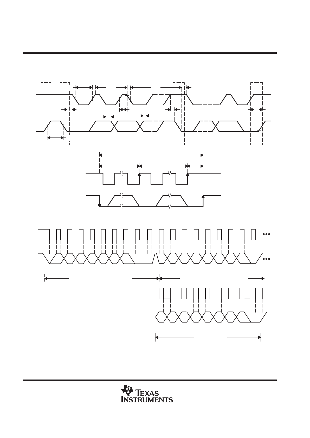
PARAMETER MEASUREMENT INFORMATION
SMBus timing diagrams
PS
t
(HDSTA)
t
(HDDAT)
t
(HIGH)
t
(SUDAT)
t
(SUSTA)
t
(HDSTA)
t
(SUSTO)
SP
SCLK
SDATA
Start
Stop
SCLK
ACK
SCLK
ACK
t
(LOWMEXT)
SCLK
SDATA
t
(LOW)
t
(LOWSEXT)
t
F
t
R
t
(BUF)
t
(LOWMEXT)
t
(LOWMEXT)
Figure 1. SMBus Timing Diagram
Frame 3 Data Byte
Frame 1 SMBus Slave Address Byte
Frame 2 Address Pointer Register Byte
A6 A5 A4 A3 A2 A1 A0 D7 D6 D5 D4 D3 D2 D1 D0R/W
SCLK
SDATA
Start By
Master
ACK By
THMC10
ACK By
THMC10
D7 D6 D5 D4 D3 D2 D1 D0
ACK By
THMC10
SCLK
(Continued)
SDATA
(Continued)
1
91 9
1
9
Stop By
Master
Figure 2. SMBus Timing Diagram for Write Byte Format

THMC10
REMOTE/LOCAL TEMPERATURE MONITOR
WITH SMBus INTERFACE
SLIS089 – DECEMBER 1999
7
POST OFFICE BOX 655303 • DALLAS, TEXAS 75265
PARAMETER MEASUREMENT INFORMATION
SMBus timing diagrams (continued)
Frame 1 SMBus Slave Address Byte
Frame 2 Address Pointer Register Byte
A6 A5 A4 A3 A2 A1 A0 D7 D6 D5 D4 D3 D2 D1 D0R/W
SCLK
SDATA
Start By
Master
ACK By
THMC10
ACK By
Master
SCLK
(Continued)
DATA
Continued)
1
91 9
Frame 3 SMBus Slave Address Byte
Frame 4 Data Byte Read From THMC10
A6 A5 A4 A3 A2 A1 A0 D7 D6 D5 D4 D3 D2 D1 D0R/W
Start By
Master
ACK By
THMC10
NACK By
THMC10
1
91 9
Stop By
Master
Figure 3. SMBus Timing Diagram for Read Byte Format
Frame 1 SMBus Slave Address Byte
Frame 2 Address Pointer Register Byte
A6 A5 A4 A3 A2 A1 A0 D7 D6 D5 D4 D3 D2 D1 D0R/W
SCLK
DATA
Start By
Master
ACK By
THMC10
ACK By
THMC10
1
91 9
Stop By
Master
Figure 4. SMBus Timing Diagram for Send Byte Format (Used for One-Shot Command)
Frame 1 SMBus Slave Address Byte
Frame 2 Data Byte From THMC10
A6 A5 A4 A3 A2 A1 A0 D7 D6 D5 D4 D3 D2 D1 D0R/W
SCLK
DATA
Start By
Master
ACK By
THMC10
NACK
By Master
1
91 9
Stop By
Master
Figure 5. SMBus Timing Diagram for Recieve Byte Format

THMC10
REMOTE/LOCAL TEMPERATURE MONITOR
WITH SMBus INTERFACE
SLIS089 – DECEMBER 1999
8
POST OFFICE BOX 655303 • DALLAS, TEXAS 75265
PRINCIPLES OF OPERATION
SMBus registers and addresses
T able 1. ADD{0:1} SMBus Slave Address Map
ADD0 ADD1 RESULTING THMC10 SMBus
SLAVE ADDRESS
0 0 0011 000
0 3-State 0011 001
0 1 0011 010
3-State 0 0101 001
3-State 3-State 0101 010
3-State 1 0101 01 1
1 0 1001 100
1 3-State 1001 101
1 1 1001 1 10
Table 2. SDATA Temperature Data Format (In 8-Bit, 2s Complement)
TEMPERATURE
(°C)
ROUNDED DIGITAL OUTPUT
130.00 127 0 111 1111
127.00 127 0 111 1111
126.60 127 0 111 1111
25.25 25 0 001 1001
0.50 1 0 000 0001
0.25 0 0 000 0000
0.00 0 0 000 0000
–0.25 0 0 000 0000
–0.50 0 0 000 0000
–0.75 –1 1 111 1111
–1.00 –1 1 111 1111
–25.00 –25 1 110 011 1
–25.25 –26 1 110 0110
–54.75 –55 1 100 1001
–55.00 –55 1 100 1001
–65.00 –65 1 011 1111

THMC10
REMOTE/LOCAL TEMPERATURE MONITOR
WITH SMBus INTERFACE
SLIS089 – DECEMBER 1999
9
POST OFFICE BOX 655303 • DALLAS, TEXAS 75265
PRINCIPLES OF OPERATION
SMBus registers and addresses (continued)
Table 3. Address Pointer Register Map
REGISTER
ADDRESS
POINTER
POR STATE FUNCTION
RIT 00h 0000 0000†Read internal temperature
RET 01h 0000 0000†Read external temperature
RS 02h 0000 0000 Read status byte
RC 03h 0000 0000 Read configuration byte
RCR 04h 0000 0010 Read acquisition rate byte
RIHL 05h 0111 1111 Read internal high limit
RILL 06h 1100 1001 Read internal low limit
REHL 07h 0111 1111 Read external high limit
RELL 08h 1100 1001 Read external low limit
WC 09h N/A Write configuration byte
WCR 0Ah N/A Write acquisition rate byte
WIHL 0Bh N/A Write internal high threshold
WILL 0Ch N/A Write internal low threshold
WEHL 0Dh N/A Write external high threshold
WELL 0Eh N/A Write external low threshold
OSHT 0Fh N/A One-shot (uses send byte format)
MFG ID FEh 0100 1001 Read manufacturer ID (0×49 for TI)
REV ID FFh N/A Read silicon revision number
†
If the THMC10 is in standby
Table 4. Configuration Register Bit Assignments
BIT NAME POR STATE FUNCTION
7 (MSB) MASK 0 Masks ALERT interrupts if high.
6 Run/stop 0 Standby mode control bit, if high, standby mode is initiated. (Note: Does not disable SMBus Interface)
5 to 0 Reserved
Table 5. Status Register Bit Assignments
BIT NAME POR STATE FUNCTION
7 (MSB) BUSY 0 A/D is busy acquiring when high.
6 LHIGH
†
0 Internal high-temperature alarm has tripped when high, cleared by power-on reset (POR) or readout of
entire status byte.
5 LLOW
†
0 Internal low-temperature alarm has tripped when high, cleared by POR or readout of entire status byte.
4 RHIGH
†
0 External high-temperature alarm has tripped when high, cleared by POR or readout of entire status byte.
3 RLOW
†
0 External low-temperature alarm has tripped when high, cleared by POR or readout of entire status byte.
2 OPEN
†
0 A high indicates an external diode open.
1 to 0 0 Reserved
†
These flags stay high until cleared by POR or until the status byte register is read.

THMC10
REMOTE/LOCAL TEMPERATURE MONITOR
WITH SMBus INTERFACE
SLIS089 – DECEMBER 1999
10
POST OFFICE BOX 655303 • DALLAS, TEXAS 75265
PRINCIPLES OF OPERATION
SMBus registers and addresses (continued)
Table 6. Acquistion Rate Register Bit Assignments
DATA
ACQUISITION RATE
(Hz)
AVERAGE SUPPLY CURRENT
(µA TYPICAL AT VDD=3.3V)
00h 0.0625 40
01h 0.125 40
02h 0.25 40
03h 0.5 40
04h 1 42
05h 2 45
06h 4 55
07h 8 65
08h to FFh Reserved N/A
Table 7. Alert Response Address Map
(Using Receive Byte Format in Figure 5)
THMC10 ALERT RESPONSE
SMBUS SLAVE ADDRESS
ADD1 ADD0
DATA IF
ALERT
LOW
0001 100 0 0 0011 000
0001 100 0 3-State 0011 001
0001 100 0 1 0011 010
0001 100 3-State 0 0101 001
0001 100 3-State 3-State 0101 010
0001 100 3-State 1 0101 011
0001 100 1 0 1001 100
0001 100 1 3-State 1001 101
0001 100 1 1 1001 110
functional description
standby input (STBY)
Standby mode disables the A/D and reduces the supply current drain to less than 10 µA.
Standby mode is engaged by forcing the STBY
terminal low or by setting the
start/stop
bit in the configuration
byte register to a 1.
Hardware and software standby modes behave almost identically . All data is retained in memory and the SMBus
interface is active and scanning for reads and writes. The only difference is that in hardware standby mode, the
one-shot command does not initiate an acquisition. The standby mode is not a shutdown mode. With activity
on the SMBus, extra supply current is drawn (see A/D and supply dc electrical characteristics). In the software
standby mode, the THMC10 can be forced to perform temperature acquisitions via the one-shot command,
despite the
start/stop
bit being high.

THMC10
REMOTE/LOCAL TEMPERATURE MONITOR
WITH SMBus INTERFACE
SLIS089 – DECEMBER 1999
11
POST OFFICE BOX 655303 • DALLAS, TEXAS 75265
PRINCIPLES OF OPERATION
standby input (STBY) (continued)
Forcing the STBY terminal low activates the hardware standby mode. In a notebook computer, this line may
be connected to the system suspend-state signal. Pulling the STBY terminal low overrides any software
acquisition command. If a hardware or software standby command is received while an acquisition is in
progress, the acquisition cycle is truncated, and the data from that acquisition is not latched into either
temperature reading register. The previous data is not changed and remains available.
Peak supply current drain during an auto-aquire period is typically 300 µA. Slowing down the auto-acquire rate
minimizes the average supply current (see
A/D and supply dc electrical characteristics). In between
acquisitions, the instantaneous supply current is about 40 µA, due to the current consumed by the auto-aquire
rate timer. In standby mode, supply current drops to about 3 µA. At very low supply voltages (under the
power-on-reset threshold), the supply current is higher due to the address terminal bias currents. It can be as
high as 100 µA, depending on ADD0 and ADD1 settings.
under/overtemperature and remote diode diagnostics interrupt alert terminal (ALERT)
The THMC10 allows the user to program upper and lower temperature limits for both the on-chip and the remote
temperature sensor. If any of these limits are exceeded, or an open external diode is detected, the THMC10
asserts the ALERT to a logic low state to alert the user that an interrupt has occurred. This feature is useful in
applications where minimal SMBus traffic is desired by only interrogating the THMC10 for faults or temperature
when a fault has occurred.
It is recommended that the user always double-check the validity of an ALERT condition by reading the current
temperature values and comparing them with the programmed high and low temperature limits.
The ALERT function can also be masked by setting bit 6 in the configuration register to a logic 1. If this bit is
set, the ALERT
terminal is not asserted low, even if a trip point is reached.
The ALERT
signal and corresponding status register bits can only be cleared by reading from the alert response
address (0001 100) or by a power-on reset of the device (see alert response address section).
NOTE:
The ALERT
terminal is an open-drain output and requires an external pullup resistor.
alert response address (0001 100)
The SMBus alert response address allows the user to quickly check the status of the ALERT
terminal via the
SMBus receive byte protocol (see Figure 5). This is useful in applications where another device on the SMBus
needs to know the status of the THMC10 ALERT
terminal without requiring the complex logic needed to decode
the contents of the status register. If the ALER T has been asserted low, the data read from the alert response
address is the THMC10 slave address (determined by ADD0 and ADD1 – see Table 8). If the fault condition
which caused the ALERT to go low is no longer present when the alert response address is successfully read,
the ALERT
terminal returns to a logic high state and the corresponding bits in the THMC10 status register are
cleared. If the ALERT terminal has not been asserted low , the THMC10 responds to the alert response address
with a NACK signal after the alert response address is sent.
The alert response address can activate several different slave devices simultaneously. It is similar to the
general call address outlined in the I2C Bus specification. If more than one device attempts to respond to the
alert response address, SMBus arbitration rules apply , causing the device with the lowest slave address to win
control of the SMBus. The device that loses arbitration in this example does not generate an ACK signal and
continues to hold the ALERT terminal low until the device with the losing slave address is serviced. This
technique requires the SMBus host controller to use level-sensitive interrupt inputs in order to assure that each
device is serviced.

THMC10
REMOTE/LOCAL TEMPERATURE MONITOR
WITH SMBus INTERFACE
SLIS089 – DECEMBER 1999
12
POST OFFICE BOX 655303 • DALLAS, TEXAS 75265
PRINCIPLES OF OPERATION
SMBus slave address select terminals (ADD0 and ADD1)
The ADD0 and ADD1 terminals allow the user to select between nine unique SMBus slave addresses to allow
up to nine THMC10 devices to be used by the same SMBus host controller. The following truth table shows how
the voltage at ADD0 and ADD1 determines the SMBus slave address of the THMC10.
Table 8. SMBus Slave Address Map (ADD0 and ADD1)
ADD0 ADD1 RESULTING SMBus ADDRESS
0 0 001 1 000
0 3-State 0011 001
0 1 001 1 010
3-State 0 0101 001
3-State 3-State 0101 010
3-State 1 0101 011
1 0 1001 100
1 3-State 1001 101
1 1 1001 1 10
SMBus serial clock input terminal (SCLK)
The SCLK terminal allows the host controller to send a clock signal that synchronizes the data coming into or
out of the SDA TA terminal of the THMC10. The frequency of this clock can be anywhere between 10 kHz and
100 kHz. Timing diagrams showing the relationship of SCLK to SDA T A are shown in Figure 1 through Figure 4.
SMBus serial data input/output terminal (SDATA)
The SDA TA terminal allows the host controller to program the THMC10 with set points and with configuration
data. The SDA TA terminal also allows the THMC10 to send data back to the host controller (remote and local
temperature, interrupt status, etc.). Data sent into or out of the SDA TA terminal is synchronous with the rising
edge of SCLK. Timing diagrams in Figure 1 through Figure 5 show the relationship between SDA T A and SCLK.
Table 1 through Table 5 show the THMC10 register maps that are used to configure and read the THMC10.

THMC10
REMOTE/LOCAL TEMPERATURE MONITOR
WITH SMBus INTERFACE
SLIS089 – DECEMBER 1999
13
POST OFFICE BOX 655303 • DALLAS, TEXAS 75265
PRINCIPLES OF OPERATION
external temperature sensor connections (DXP and DXN)
The DXP and DXN terminals are used to sense the remote temperature of either a microprocessor die or a
simple diode-connected transistor. Referring to Figure 6, the THMC10 has an internal state machine controlling
an analog MUX, an 8-bit A/D converter, plus 10-µA and 90-µA nominal current sources. The analog MUX
switches between the THMC10’s internal temperature sensor and the external one connected to DXP and DXN.
This allows the use of only one 8-bit A/D converter, eliminating errors which would be present when using two
separate A/Ds. The THMC10 takes a V
BE
measurement at 100 µA, then takes a VBE measurement at 10 µA,
and subtracts the difference between the two sampled values. It then scales the resulting ∆VBE measurement
into a 2s complement, 8-bit binary format that is available over the SMBus interface (see T able 2). By using two
different current levels and a single diode-connected transistor to measure the ∆V
BE
, the absolute VBE is
canceled, and therefore no calibration is needed.
8–Bit A/D
Converter
DXP
Substrate
On-Chip Temp
Sensor
GND
V
DD
10 µ 90 µA
Control
State
Machine
Analog
MUX
Remote
Die
Substrate
DXN
Remote
Temp
Sensor
(CPU)
THMC10
Front End
A
Figure 6. Temperature Measurement Block Diagram
external temperature sensor diagnostics (DXP and DXN)
The THMC10 provides diagnostic capabilities to allow detection of either an open external sensor or a shorted
external sensor. When DXP is shorted to GND or VDD, the THMC10 reports 127°C for the external temperature.
If the interrupt mask bit is not set in the configuration register, it asserts the ALERT terminal low and sets bit two
in the status register. When DXP is shorted to DXN, the THMC10 reports 0°C for the external temperature and
no fault is reported. If any of the above conditions exceed a temperature limit, then a temperature limit error is
also indicated in the status register if the interrupt mask bit is not set.

THMC10
REMOTE/LOCAL TEMPERATURE MONITOR
WITH SMBus INTERFACE
SLIS089 – DECEMBER 1999
14
POST OFFICE BOX 655303 • DALLAS, TEXAS 75265
PRINCIPLES OF OPERATION
PC board layout considerations
D
Place the THMC10 as close as practical to the remote diode. In a noisy environment, such as a computer
motherboard, this distance can be 4 inches to 8 inches (typical) or more, as long as the worst noise sources
(such as CRTs, clock generators, memory buses, and ISA/PCI buses) are avoided.
D
Route the DXP–DXN lines away from the deflection coils of a CRT. Also, avoid routing the traces across
a fast memory bus which can easily introduce 30°C error even with good filtering. Otherwise, most noise
sources are fairly benign.
D
Route the DXP and DXN traces in parallel and in close proximity to each other, away from any high-voltage
traces such as 12 Vdc. Leakage currents from PC board contamination must be be taken into consideration,
since a 20-MΩ leakage path from DXP to ground causes about 1°C error.
D
Connect guard traces to GND on either side of the DXP–DXN traces (Figure 7). With guard traces in place,
routing near high-voltage traces is not an issue.
D
Route through as few vias and crossunders as possible to minimize copper/solder thermocouple effects.
D
When introducing a thermocouple, insure that both the DXP and the DXN paths have matching
thermocouples. In general, PC board induced thermocouples are not a serious problem. A copper-solder
thermocouple exhibits 3 µV/°C, and it takes about 200 µV of voltage error at DXP–DXN to cause a 1°C
measurement error. Hence, most parasitic thermocouple errors are swamped out.
D
Use wide traces. Narrow traces are more inductive and tend to pick up radiated noise. The 10-mil widths
and spacings recommended in Figure 7 are not absolutely necessary as they offer only a minor
improvement in leakage and noise, but usage is recommended where practical.
D
Copper can not be used as an EMI shield and only ferrous materials such as steel work well. Placing a
copper ground plane between the DXP–DXN traces and traces carrying high-frequency noise signals does
not help reduce EMI.
PC board layout checklist
D
Place the THMC10 as close as possible to the remote diode.
D
Keep traces away from high voltages (12 V bus).
D
Keep traces away from fast data/memory buses and CRTs.
D
Use recommended trace widths and spacings.
D
Place a ground plane under the traces.
D
Use guard traces flanking DXP and DXN and connecting to GND.
D
Place the noise filter and the 0.1-µF VDD bypass capacitors close to the THMC10.

THMC10
REMOTE/LOCAL TEMPERATURE MONITOR
WITH SMBus INTERFACE
SLIS089 – DECEMBER 1999
15
POST OFFICE BOX 655303 • DALLAS, TEXAS 75265
PRINCIPLES OF OPERATION
PC board layout checklist (continued)
10 MILS
DXN
DXP
GND
GND
10 MILS
MINIMUM
10 MILS
10 MILS
Figure 7. Recommended PC Board Layout for DXP/DXN Traces
uses of twisted pair and shielded cables
For remote-sensor distances longer than 8 inches or in particularly noisy environments, a twisted pair is
recommended. Its practical length is 6 feet to 12 feet (typical) before noise becomes a problem, as tested in
a noisy electronics laboratory. For longer distances, the best solution is a shielded twisted pair like that used
for audio microphones. For example, a Belden #8451 works well for distances up to 100 feet in a noisy
environment. Connect the twisted pair to DXP and DXN and the shield to GND, and leave the shield’s remote
end unterminated. Excess capacitance at DXN limits practical remote sensor distances (see A/D and supply
dc electrical characteristics). For very long cable runs, the cable’s parasitic capacitance often provides noise
filtering; hence, the 2200-pF capacitor can often be removed or reduced in value. Cable resistance also affects
remote-sensor accuracy. A 1-Ω series resistance introduces about 0.5°C error.
Belden is a registered trademark of Belden Corporation.

THMC10
REMOTE/LOCAL TEMPERATURE MONITOR
WITH SMBus INTERFACE
SLIS089 – DECEMBER 1999
16
POST OFFICE BOX 655303 • DALLAS, TEXAS 75265
APPLICATION INFORMATION
THMC10
SCLK
SDATA
ALERT
ADD1
ADD0
SCLK
V
DD
C2
2200 pF
Q1
2N3904
or
Equivalent
3
4
DXP
DXN
GNDGND
87
14
12
11
6
10
V
DD
STBY
15
2
SDATA
ALERT
ADD1
ADD0
STBY
C1
0.1 µF
R3
10 kΩ
R2
10 kΩ
R1
10 kΩ
To VDD,
GND, or
FLOAT
Figure 8. Typical Application Schematic

THMC10
REMOTE/LOCAL TEMPERATURE MONITOR
WITH SMBus INTERFACE
SLIS089 – DECEMBER 1999
17
POST OFFICE BOX 655303 • DALLAS, TEXAS 75265
PERFORMANCE DATA
temperature error vs power supply sinusoidal noise frequency
–2
–1
0
1
2
3
f – Frequency – Hz
10 100 1k 100k 100M1M10k 10M
62 mV
p-p
Remote
125 mV
p-p
Local
125 mV
p-p
Remote
62 mV
p-p
Local
250 mV
p-p
Local
250 mV
p-p
Remote
t – Temperature Error –
C
°
250 mV
p-p
Local
250 mV
p-p
Remote
Figure 9. Data Plot
STDBY V
DD
15 2
V
DD
SMBCLK
SMBDATA
ALERT
V
DD
GND
GND
ADD0 ADD1
Q1
2N3904
R4
50 Ω
HP8116A
Generator
To ICA93LV
I2C Controller
14
12
11
7
8
10 6
4
3
DXP
DXN
THMC10
R1
10 kΩ
R2
50 Ω
R3
1 kΩ
C1
20 pF
NOTE: No 0.1 µF VDD capacitor.
Figure 10. Test Circuit

THMC10
REMOTE/LOCAL TEMPERATURE MONITOR
WITH SMBus INTERFACE
SLIS089 – DECEMBER 1999
18
POST OFFICE BOX 655303 • DALLAS, TEXAS 75265
PERFORMANCE DATA
temperature error vs PNP collector square wave noise frequency
–1
0
1
f – Frequency – Hz
10 100 1k 100k 100M1M10k 10M
100 mV
p-p
Local
100 mV
p-p
Remote
t – Temperature Error –
C
°
Figure 11. Data Plot
STDBY V
DD
15 2
3.3 V
SMBCLK
SMBDATA
ALERT
3.3 V
GND
GND
ADD0 ADD1
Q1
2N3906
R2
50 Ω
HP8116A
Generator
To ICA93LV
I2C Controller
14
12
11
7
8
10 6
4
3
DXP
DXN
THMC10
R1
10 kΩ
NOTE: No 0.1 µF VDD capacitor.
No 2200 pF DXP-DXN filter capacitor.
Representative of
Processor On-Die
Sensing Diode
Figure 12. Test Circuit

THMC10
REMOTE/LOCAL TEMPERATURE MONITOR
WITH SMBus INTERFACE
SLIS089 – DECEMBER 1999
19
POST OFFICE BOX 655303 • DALLAS, TEXAS 75265
MECHANICAL DATA
DBQ (R-PDSO-G**) PLASTIC SMALL-OUTLINE PACKAGE
Gage Plane
0.008 (0,20) NOM
0.010 (0,25)
0.016 (0,40)
0.035 (0,89)
2420
Seating Plane
(8,74)
(8,56)
0.3370.337
(8,56)
(8,74)
0.344 0.344
4073301/D 08/98
13
0.150 (3,81)
0.157 (3,99)
0.012 (0,30)
0.008 (0,20)
12
A
24–PIN SHOWN
1
24
16
DIM
PINS **
A MIN
A MAX
0.004 (0,10)
0.010 (0,25)
0.069 (1,75) MAX
0.244 (6,20)
0.228 (5,80)
0.197
(5,00)
(4,78)
0.188
0.004 (0,10)
M
0.005 (0,13)
0.025 (0,64)
0°–8°
NOTES: A. All linear dimensions are in inches (millimeters).
B. This drawing is subject to change without notice.
C. Body dimensions do not include mold flash or protrusion not to exceed 0.006 (0,15).
D. Falls within JEDEC MO-137

IMPORTANT NOTICE
T exas Instruments and its subsidiaries (TI) reserve the right to make changes to their products or to discontinue
any product or service without notice, and advise customers to obtain the latest version of relevant information
to verify, before placing orders, that information being relied on is current and complete. All products are sold
subject to the terms and conditions of sale supplied at the time of order acknowledgement, including those
pertaining to warranty, patent infringement, and limitation of liability.
TI warrants performance of its semiconductor products to the specifications applicable at the time of sale in
accordance with TI’s standard warranty. Testing and other quality control techniques are utilized to the extent
TI deems necessary to support this warranty. Specific testing of all parameters of each device is not necessarily
performed, except those mandated by government requirements.
CERT AIN APPLICATIONS USING SEMICONDUCTOR PRODUCTS MAY INVOLVE POTENTIAL RISKS OF
DEATH, PERSONAL INJURY, OR SEVERE PROPERTY OR ENVIRONMENTAL DAMAGE (“CRITICAL
APPLICATIONS”). TI SEMICONDUCTOR PRODUCTS ARE NOT DESIGNED, AUTHORIZED, OR
WARRANTED TO BE SUITABLE FOR USE IN LIFE-SUPPORT DEVICES OR SYSTEMS OR OTHER
CRITICAL APPLICATIONS. INCLUSION OF TI PRODUCTS IN SUCH APPLICA TIONS IS UNDERSTOOD T O
BE FULLY AT THE CUSTOMER’S RISK.
In order to minimize risks associated with the customer’s applications, adequate design and operating
safeguards must be provided by the customer to minimize inherent or procedural hazards.
TI assumes no liability for applications assistance or customer product design. TI does not warrant or represent
that any license, either express or implied, is granted under any patent right, copyright, mask work right, or other
intellectual property right of TI covering or relating to any combination, machine, or process in which such
semiconductor products or services might be or are used. TI’s publication of information regarding any third
party’s products or services does not constitute TI’s approval, warranty or endorsement thereof.
Copyright 2000, Texas Instruments Incorporated
 Loading...